1
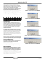
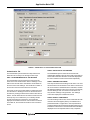
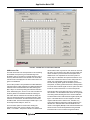
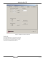
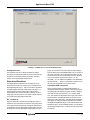
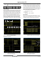
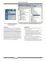
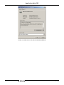
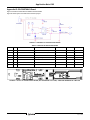
ISL6296 Evaluation Kit
®
Application Note
July 14, 2009
AN1165.1
Introduction
The ISL6296 evaluation kit provides a convenient tool to
evaluate the ISL6296 Flexihash™ engine for authentication.
The evaluation kit contains four items:
• A Compact Disk (CD) with the evaluation system software
for Win98 SE, Win ME, 2000, or XP.
• An interface board that connects a USB port to the XSD
bus.
• Two evaluation boards with the ISL6296 part.
• A cable to connect the interface board to the evaluation
board.
The ISL6296 Evaluation System software gives the user
complete control of the ISL6296. The interface board
translates the PC commands to XSD commands and
provides the power to the ISL6296 using the USB bus
power. No additional power supply is required to perform the
evaluation. An oscilloscope helps to monitor the XSD bus
activity. This application note serves as the user manual of
the evaluation kit.
NOTE: Please email to [email protected] if you find bugs
during evaluation or have suggestions.
FIGURE 1. PHOTO OF THE EVALUATION KIT
(CD NOT INCLUDED)
Evaluation Kit Setup
The following are steps for setting up the evaluation system:
ISL6296EVAL1 Evaluation Board
The ISL6296EVAL1 board is a 1cm X 4cm single-layer
board, as shown in Figure 1. The schematic, layout and billof-materials (BOM) are given in Appendix B. The board has
5 test points to allow the user to conveniently hook up the
scope probes or other test equipment. Two of them are
connected to the ground and the remaining three connect to
the other three pins of the ISL6296.
2. Plug the Interface Board into the USB port. The Windows
Operating System (OS) will automatically recognize the
board as a Human Interface Device.
3. Follow the steps given in Appendix A to confirm the
installation of the Interface Board in the OS. This step is
optional.
4. Hook up a scope probe to the XSD test point to monitor
the XSD bus activity.
ISL6296 Interface Board
The Interface board is also shown in Figure 1. One side of
the board is a USB connector and the other side is a threepin connector for the XSD bus. The XSD-bus connector
contains power, XSD and ground lines. The power line
provides power to the ISL6296EVAL1 and its voltage is
adjustable through the Configuration tab in the evaluation
system software (See Evaluation System Software section
for more details). The schematic, layout and BOM are given
in Appendix C.
Software Installation
Installing the software is straightforward and requires only
two steps:
1. Open the folder named Installation in the CD;
2. Double click SETUP.EXE and follow the instructions.
1
1. Connect the ISL6296EVAL1 board to the ISL6296
Interface Board using the provided cable.
5. Start up the ISL6296 Evaluation System software that
was installed a moment ago and you are ready to
evaluate the ISL6296.
Evaluation System Software
The software has five major functional tabs to provide all
necessary tools for the evaluation. Figures 7 to 11 show the
screen shots for each tab. This section first discusses a few
things the user needs to know before using the software,
and then explains in detail how to use each tab of the
software.
Device Address and XSD Bus Speed
Before evaluating the ISL6296, the user needs to confirm
that the XSD bus speed of the host matches the speed of the
ISL6296, and the device address (0 or 1) in the ISL6296 is
set to the proper value. The default configuration (DCFG)
CAUTION: These devices are sensitive to electrostatic discharge; follow proper IC Handling Procedures.
1-888-INTERSIL or 1-888-468-3774 | Intersil (and design) is a registered trademark of Intersil Americas Inc.
Copyright Intersil Americas Inc. 2005, 2009. All Rights Reserved
FlexiHash is a trademark of Intersil Americas Inc. All other trademarks mentioned are the property of their respective owners.
Application Note 1165
address (at bank 0, address 0) contains the device
configuration when it is powered up. When an ISL6296 is
shipped from the factory, the DCFG is set to the value given
in Table 1. Users can always start with the default
configuration. Once the two ends can communicate properly,
the user can start using the tools. Most parts of the
evaluation software only address device ‘0’. If the device
address is not ‘0’, the user needs to use the XSD Access tab
to change the address to ‘0’. Appendix D provides the
techniques if using the default configuration could not make
the PC and the ISL6296 communicate properly.
FIGURE 2. “A break is received” POP-UP MESSAGE
TABLE 1. DCFG DEFAULT VALUE WHEN SHIPPED FROM
FACTORY
NAME
Value
Function
BIT 7 BIT 6 BIT 5 BIT 4 BIT 3 BIT 2 BIT 1 BIT 0
0
0
DAB[1:0]
0
1
SPD[1:0]
1
1
eINT ASLP
0
0
FIGURE 3. “Read register failed” POP-UP MESSAGE
SLO[1:0]
Pop-Up Messages
Under certain conditions, the software pops up an error
message to indicate to the user that an error just happened.
Another possible pop-up message shows up when the user
tries to write to the Default Configuration (DCFG) address.
This section explains all the possible pop-up messages.
FIGURE 4. “Send XSD command failed” POP-UP MESSAGE
A BREAK IS RECEIVED
The ISL6296 sends a ‘break’ signal to the host when any
error happens. When the interface receives a ‘break’ signal,
it notices the PC software to pop-up the “A break is received”
message, as shown in Figure 2. Usually when a ‘break’
signal is received, the host needs to try to read the status
register to find the type of error as well as to clear the error.
READ REGISTER FAILED
FIGURE 5. “Write to USB bus failed” POP-UP MESSAGE
When the host tries to read a register in the ISL6296 and did
not receive the correct data within a time limit, the host pops
up the “Read register failed” message, as shown in Figure 3.
SEND XSD COMMAND FAILED
This message, as shown in Figure 4, pops up when the PC
software tries to send the XSD command but fails.
WRITE TO USB BUS FAILED
FIGURE 6. “Write Confirmation” POP-UP MESSAGE
The message in Figure 5 shows up when the PC fails to
communicate with the USB device (the interface board).
WRITE CONFIRMATION
Writing to the default configuration address can potentially
change the device address, XSD bus speed, interrupt and
auto-sleep configuration, or lockout the secret addresses. In
order to prevent the user from changing the default
configuration by accident, the software pops up the message
shown in Figure 6 to ask for confirmation. The DCFG value
will be changed when the user clicks “Yes”.
2
AN1165.1
July 14, 2009
Application Note 1165
Send Challenge
FIGURE 7. SCREEN SHOT OF THE AUTHENTICATION TAB
Authentication Tab
STEP 2: SELECTION OF THE SECRETS
The authentication process takes four steps and this tab
allows the user to easily move through the four steps.
The ISL6296 has space for three sets of secret and the
authentication algorithm uses one for the Hash engine and one
as the seed for the CRC calculator. The second step requires
the user to select the secret for each function respectively.
STEP 1: SYNCHRONIZATION OF THE SECRETS
The authentication process requires the same secret be
stored in the host and the device. When a challenge is sent,
both the host and the device calculate the results based on
the same secret and challenge. The results will not match if
the secrets in the host and the device do not match.
The secret can be synchronized either by reading the secret
from the device or sending the secret on the host screen to
the device by clicking the Read Secret and the Send Secret
buttons. This tab allows the user to read the secrets from the
device (if they are not locked out) or to manually edit the
secrets and send them to the device. The secrets are
displayed in hexadecimal format. If the secrets in the device
are locked out, the host will not be able to read or send the
secret.
3
STEP 3: SENDING CHALLENGE
This step sends the 32-bit challenge to the device. The host
will first send the secret selection to the device to ensure that
the correct seed is re-loaded before the calculation, and then
the displayed challenge code is sent. The user can manually
edit the challenge code. The Random Code button is for
easy random challenge code generation. The challenge
code is also displayed in hexadecimal format.
STEP 4: RESULT COMPARISON
Once the challenge code is sent, the PC reads back the hash
result from the result register (AUTH). The software has a
powerful FlexiHash™ engine built in. The Expected Result
cell always displays the expected result instantly based on the
information on the screen. The result read from the ISL6296 is
displayed next to the expected result for easy comparison.
AN1165.1
July 14, 2009
Application Note 1165
FIGURE 8. SCREEN SHOT OF THE REGISTERS ACCESS TAB
Registers Access Tab
This tab allows the user to read or write to the EEPROM in
bank 0, the master control register (MSCR), and the status
register (STAT). The default trim (DTRM) byte and the STAT
are read-only addresses and are marked with “(ro)”. The
data are displayed in both binary and hexadecimal forms. To
change the value in these addresses, the user can either
input in the binary fields or the hexadecimal fields. When the
Read button is clicked, the host reads all the addresses and
updates the results on this tab. When the Write button is
clicked, the host only sends data to the addresses whose
values have been changed. Whenever the user tries to
update the DCFG address, the message shown in Figure 6
will pop up to ask for confirmation.
4
AN1165.1
July 14, 2009
Application Note 1165
FIGURE 9. SCREEN SHOT OF THE XSD ACCESS TAB
XSD Access Tab
The XSD Access tab is the most powerful tool for evaluating
the ISL6296 and requires a good understanding of the
ISL6296 in order to use this tool. This tab allows the user to
send any XSD instructions to the ISL6296. The 16-bit XSD
instruction frame is displayed in the same format as the one
given in the datasheet.
The tool also provides a 16-byte table for the XSD data frame.
If the instruction is a Write instruction, the data that follows the
instruction frame should be listed in the table, starting from
Byte 1. Byte 1 is the first byte being sent after the instruction
frame, followed by byte 2, and so on. The user can either use
the binary fields or the hexadecimal fields for entering the
data. When both the instruction and the data are ready, the
user can click the Send button to send the instruction. If the
instruction is a Read frame, the data read are to be listed in
the table as well. The first received byte is listed in Byte 1, the
second byte is listed in Byte 2, and so on.
There are three options to choose when sending the
instructions frame, with “power on break”, with “regular
break”, or “no break”. The power-on break is a narrow break
5
that should be used only when the user knows for sure that
the device is in the sleep mode. After the narrow break, the
device will wake up and send back a break (Refer to the
datasheet for more explanation of the narrow power-on
break). Figure 14 illustrates the captured waveforms. If the
user does not know if the device is in the sleep mode or is
awake, the “regular break” option should be chosen,
because the long break signal will still wake up a device in
sleep mode, or will be ignored if the device is already awake.
The send without a break signal can be an option if the user
knows for sure that the device is not in the sleep mode.
This tab also offers a few other tools for the convenience of
the evaluation. The Send Break button sends out a long break
when being clicked, allowing the user to reset the XSD bus.
The Read Status button reads the status register (STAT) into
Byte 1 of the table. When a bus error happens, the STAT
register needs be read to clear the error; otherwise, any
access to the XSD bus will result in a break signal from the
ISL6296. The Soft Reset button sets the SRST bit in the
master control register (MSCR) to soft-reset the ISL6296. The
above two tools can also be implemented using the XSD
instructions but is more convenient using these buttons.
AN1165.1
July 14, 2009
Application Note 1165
FIGURE 10. SCREEN SHOT OF THE TOOL BOX TAB
Tool Box Tab
This tab is self-explanatory. The most useful tool in this tab is
the Set XSD Communication Configuration tool that allows
the user the set the host and the slave speeds. The other
useful tool is the Enable/Disable Auto Sleep tool.
6
AN1165.1
July 14, 2009
Application Note 1165
FIGURE 11. SCREEN SHOT OF THE CONFIGURATION TAB
Configuration Tab
This tab allows the user to adjust the XSD bus voltage.
Eventually, this tab will also allow the user to download new
firmware to the interface board for upgrading. The latter
function is not implemented at this moment.
Evaluation Waveforms
The digital signals transferred over the XSD bus can be
verified with the help of an oscilloscope. The XSD bus has
three digital signals, logic ‘1’, logic ‘0’ and ‘break’. Each bit of
the digital signals starts with a falling edge. The logic ‘1’ is
represented with a signal whose rising edge occurs at
approximately 30% of the bit time (BT). The logic ‘0’ has a
rising edge occurring at about 70% of BT. A ‘break’ signal is
one whose rising edge happens after 1BT.
Bit ‘1’ and Bit ‘0’
Figure 12 shows the waveforms for the XSD bus during a
transaction. The lower half is a zoomed-in view of the portion
of the upper waveform inside the rectangular dash-line box
and illustrates how the XSD signal is implemented. The first
bit being sent out is the least-significant bit (LSB) of a byte.
7
Figure 12 was captured when the XSD bus was reading 4
bytes of data from the ISL6296 EEPROM. The “A” section of
the upper waveform is the 16-bit instruction frame. The “B”
section is the 4 bytes from the ISL6296. From the waveform,
one can tell that the chip selection field CS = ‘0’, the
OPCODE = ‘01’, the address bank BANK = ‘00’ (EEPROM),
and the address = ‘...01010’. The total byte number is out of
the zoomed-in window but it was ‘100’ (4 bytes).
A Complete XSD Transaction
Figure 13 demonstrates a complete XSD transaction of
reading the MSCR and STAT registers. The instruction frame
for reading these two registers are given in Table 2. Starting
from LSB, the instruction frame is: ‘0, 10, 10, 0000, 0000,
010’. This matches the signals from the scope. Also from the
scope waveform, the MSCR and STAT are found out to be,
starting from LSB, ‘0000, 0011’, and ‘0000, 0000’ respectively
(see Figure 13). Using the XSD Access Tab in the software,
the MSCR will be filled into Byte 1 of the table and STAT will
be filled into Byte 2. From the MSCR register, one can tell that
the Autosleep (ASLP) bit is ‘0’, meaning the auto-sleep mode
is turned off.
AN1165.1
July 14, 2009
Application Note 1165
TABLE 2. INSTRUCTION FRAME FOR READING MSCR AND
STAT
BYTE
ADDRESS
BANK
OPCODE
CS
010
0000,0000
01
01
0
Power-on Break
When the ISL6296 is in sleep mode, the host needs to send
a ‘break’ signal to wake up the ISL6296. A ‘break’ signal is a
pulse wider than 1BT. When coming out of the sleep mode,
the ISL6296 sends a ‘break’ as well. The two ‘break’ signals
overlap with each other (merged) and appear to be one
pulse. The ‘break’ signal from the ISL6296 is 1.391BT wide,
therefore, contains the information for the XSD bus speed
(= 1/BT) in the ISL6296. In order to see the ‘break’ signal
from the ISL6296, a special narrow ‘break’ (power-on break)
A
signal is provided in the XSD Access tab as an option of the
Send button. When this option is selected, the host sends
out a ‘power-on break’ before sending the instruction frame.
Figure 14 illustrate the two ‘break’ signals. The narrow one
was sent by the host and the wider one was the one returned
from the ISL6296 (approximately 480μs). From the 480μs
‘break’ signal, the BT can be calculated as
BT = 480μs/1.391 = 345 μs
or baud rate is
Baud Rate = 1/BT = 2.90 kbps
Error ‘Break’
When an error occurs during the XSD transaction, a ‘break’
signal is sent by the ISL6296. Figure 15 shows the waveform.
A message, as shown in Figure 2, pops up in this case.
B
0
1
0
0
0
0
1
0
1
0
FIGURE 12. CAPTURED SCOPE WAVEFORMS TO SHOW ‘1’
AND ‘0’ OF XSD BUS SIGNALS
A falling edge sets the start of a bit time and the timing of the rising
edge determines the bit value.
0101000000000010 00000011 00000000
FIGURE 13. CAPTURED SCOPE WAVEFORMS WHEN
READING THE MSCR AND STAT REGISTERS
Break
from
ISL6296
Vertical: 1V/div
Horizontal: 200us/div
FIGURE 14. POWER-ON BREAK SIGNAL TO WAKE-UP THE
ISL6296 FROM SLEEP MODE
8
FIGURE 15. ‘BREAK’ SIGNAL SENT BY ISL6296 DUE TO A
BUS TRANSACTION ERROR
AN1165.1
July 14, 2009
Application Note 1165
FIGURE 16. SCREEN SHOT OF WHEN RIGHTCLICKING THE MY COMPUTER
ICON ON THE DESKTOP
FIGURE 17. SCREEN SHOT OF THE COMPUTER MANAGEMENT FOLDER
Summary
Appendix A
The ISL6296 Evaluation Kit provides a convenient platform
for users to evaluate the ISL6296. The Authentication Tab
demonstrates the authentication process and provides a
powerful FlexiHash™ calculator. The Register Access tab
allows the user the read from or write to the memories easily.
The XSD Access tab provides the tool for evaluating every
aspect of the ISL6296. The Tool Box and the Configuration
tabs provides other tools such as changing the XSD bus
speed or adjust the XSD bus voltage. Most tools, except for
the XSD access tool, addresses to device ‘0’. Users need to
change the device address to ‘0’ with the XSD Access tool, if
the original address is not ‘0’. Using an oscilloscope, one
can always monitor the activity on the XSD bus.
Steps to confirm the Interface Board in the OS after being
inserted to the USB port:
9
1. Right click the “My Computer” icon in the desktop window
and select “Manage,” as shown in Figure 16.
2. Select the Device Manager and the Human Interface
Devices folder will leads to the window in Figure 17.
3. Double-click on the USB Human Interface Device, then
Figure 18 will appear.
In Figure 18, one can find “Location: Evaluation Kit
ISL6296...”. This is the confirmation that the interface board
is properly recognized by the operating system.
The figures are captured in the Win2000 and are very similar
in other versions of Microsoft Windows Operating Systems.
AN1165.1
July 14, 2009
Application Note 1165
FIGURE 18. SCREEN SHOT OF THE USB HID PROPERTIES WINDOW
10
AN1165.1
July 14, 2009
Application Note 1165
Appendix B: ISL6296EVAL1 Board
Figure 19 shows the schematic and Table 3 shows the BOM.
Figure 20 is the layout of the silk screen and the top layer.
FIGURE 19. SCHEMATIC OF THE EVALUATION BOARD
TABLE 3. BOM FOR THE EVALUATION BOARD
ITEM #
QTY
PART REFERENCE
DESCRIPTION
PART NUMBER
1
1
C1
0.1µF, 16V, X7R ceramic cap
0603B104K160
0603
Walsin
2
1
C2
1µF, 6.3V, X5R ceramic cap
0603X105K6R3
0603
Walsin
3
2
D1, D2
Zener diode, 5.1V
CMDZ5231B
SOD-323
Central Semi
4
1
J1
Single Right Angle 3 Pin Header
WM1754-ND
5
2
R1, R2
6
5
TP1, TP2, TP3, TP4, TP5
7
1
U1
100Ω, 5%
PACKAGE
Digikey
0603
Miniature Surface Mount Test Point
5015KCT-ND
SOT-23, ISL6296
ISL6296
VENDOR
Various
Digikey
SOT-23
Intersil
FIGURE 20. LAYOUT OF THE EVALUATION BOARD (SILK SCREEN AND TOP LAYER). THE BOARD DIMENSION IS 1CM X 4CM.
11
AN1165.1
July 14, 2009
Application Note 1165
Appendix C: Interface Board
The function of the interface board is to translate the PC
commands to the XSD commands via the USB port. The
schematic for the interface board is shown in Figure 21. The
layout and the BOM are give in Figure 22 and Table 4,
respectively.
Do not populate
R7, R8, Q3, and
Q4
FIGURE 21. SCHEMATIC OF THE USB-TO-XSD INTERFACE BOARD
FIGURE 22. LAYOUT OF THE USB-TO-XSD INTERFACE BOARD
12
AN1165.1
July 14, 2009
Application Note 1165
TABLE 4. BOM OF THE USB-TO-XSD INTERFACE BOARD
ITEM #
QTY
REFERENCE
DESCRIPTION
PART #
PACKAGE
VENDOR
1
1
C1
4.7µF, 10V, X7R ceramic cap
1206X475K100
1206
Walsin
2
3
C2, C5, C6
0.1µF, 16V, X7R ceramic cap
0603B104K160
0603
Walsin
3
2
C3, C4
33pF, 50V, NPO ceramic cap
0805CG330J9BB0
0805
Garrett elec
4
1
C7
1µF, 6.3V, X5R ceramic cap
0603X105K6R3
0603
Walsin
5
1
R1
1.5K resistor
0603
Various
6
1
R2
4.7K resistor
0603
Various
7
4
R3, R4, R7, R8 (Note)
50K
0603
Various
8
1
R5
5K
0603
Various
9
1
R6
100Ω
0603
Various
10
1
R9
0Ω
0805
Various
11
1
R10
10K
0805
Various
12
1
XT1
24MHz Crystal Oscillator
300-6145-1-ND
13
4
Q1, Q2, Q3, Q4 (Note)
General purpose NPN transistor
CMST3904
SOT-323
Central
14
1
U1
Microcontroller
ST72F63BK4M1
SO-34
ST
15
1
USBCON
USB connector
16
1
J1
17
2
TP1 (VPP), TP2 (GND)
Digikey
Single Right Angle 3 Pin Header
WM1754-ND
Digikey
SMD test point
5015KCT-ND
Digikey
NOTE: Do not populate R7, R8, Q3, and Q4.
Appendix D: Techniques to Make the Host
and ISL6296 Communicate Properly
This appendix describes ways to make the host and the
device talk properly, if there is trouble.
1. If the device is in the sleep mode, send a ‘power on break’
with a read instruction in the XSD Access tab to measure
the returned ‘break’ signal for ISL6296, as shown in
Figure 14.
2. Use the method shown on page 8 to calculate the bus
speed and then choose the closest host speed using the
Tool Box tab.
3. Read the status register using address ‘0’, if no status is
returned, then,
4. Try to read the status register using address ‘1’ to confirm
the device address is indeed ‘1’.
If sending a ‘power on break’ does not lead to a ‘break’ from
the device, then the device is awake. The user needs to try
all eight combinations (4 speeds and 2 device addresses) to
establish the proper communication.
Intersil Corporation reserves the right to make changes in circuit design, software and/or specifications at any time without notice. Accordingly, the reader is cautioned to
verify that the Application Note or Technical Brief is current before proceeding.
For information regarding Intersil Corporation and its products, see www.intersil.com
13
AN1165.1
July 14, 2009