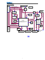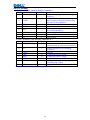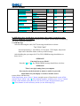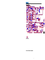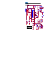
1
Service Manual
Service Manual
LCD Monitor 2209WA
-0-
1
Service Manual Versions and Revision
No.
Version
Release Date
Revision
1
1.0
2008/10/17
Initial Release
Copyright
Copyright 2007 InnoLux Display. Corp. Ltd
All Rights Reserved
This manual may not, in whole or in part, be copied, Photocopied, reproduced, translated, or converted to a
electronic or machine readable form without prior written permission of Foxconn Tech. Corp. Ltd.
Dell 2209WA Service Manual
Service Manual
Table of Contents
CHAPTER 1- PRECAUTIONS & SAFETY NOTICES ............................................................................................................
1.
2.
3.
SAFETY PRECAUTIONS ...........................................................................................................................................
PRODUCT SAFETY NOTICE................................................................................................................................
SERVICE NOTES ........................................................................................................................................................
CHAPTER 2- SERVICE TOOLS & EQUIPMENT REQUIRED ............................................................................................
CHAPTER 3- CIRCUIT THEORY .............................................................................................................................................
1.
2.
3.
4.
5.
6.
7.
8.
BLOCK DIAGRAM ..........................................................................................................................................................
ELECTRONIC CIRCUIT THEORY ................................................................................................................................
FACTORY PRESET TIMING TABLE .........................................................................................................................
POWER ON/OFF SEQUENCY ...........................................................................................................................................
D-SUB CONNECTOR PIN ASSIGNMENT .........................................................................................................................
AC OUTLET PIN ASSIGNMENT ................................................................................................................................
INNER CONNECTOR PIN ASSIGNMENT ...........................................................................................................................
KEY PARTS PIN ASSIGNMENTS................................................................................................................................
CHAPTER 4- DISASSEMBLY & ASSEMBLY ..........................................................................................................................
1.
2.
3.
EXPLODED DIAGRAM ....................................................................................................................................................
2209WA DISASSEMBLY BLOCK................................................................................................................................
ASSEMBLY BLOCK .........................................................................................................................................................
CHAPTER 5- TEST AND ADJUSTMENT ................................................................................................................................
1.
2.
3.
4.
5.
FUNCTION KEY DEFINITIONS .........................................................................................................................................
OSD CONTROL..............................................................................................................................................................
FACTORY MODE INTRODUCTION ................................................................................................................................
BURN-IN PATTERN .........................................................................................................................................................
AUTO COLOR BALANCE (AUTOMATICALLY CALIBRATE CHIP ADC PARAMETER BY USING CHIP
INTERNAL DAC.) .........................................................................................................................................................................
6.
UPLOAD FIRMWARE TO MCU VIA VGA CABLE .............................................................................................................
7.
AFTER REPAIR, TO ENSURE THE QUALITY YOU SHOULD DO THE FOLLOWING TEST AND
ADJUSTMENT. ...............................................................................................................................................................................
CHAPTER 6- TROUBLE SHOOTING ................................................................................................................................
1.
2.
3.
4.
5.
6.
COMMON ACKNOWLEDGE .............................................................................................................................................
NO POWER LED OFF .....................................................................................................................................................
POWER NORMAL LED AMBER ................................................................................................................................
BACKLIGHT CAN’T BE TURNED ON ................................................................................................................................
NO PICTURE BACKLIGHT ON ................................................................................................................................
AT 32-GRAY SCALE PATTERN, COLOR LOST IN SOME SCALE ............................................................................................
CHAPTER 7- RECOMMENDED PART LIST ..........................................................................................................................
ATTACHMENT 1- BILL OF MATERIAL ................................................................................................................................
ATTACHMENT 2- SCHEMATIC ...............................................................................................................................................
ATTACHMENT 3- PCB LAYOUT ..............................................................................................................................................
2
Service Manual
Chapter 1- PRECAUTIONS & SAFETY NOTICES
SAFETY PRECAUTIONS
This monitor is manufactured and tested on a ground principle that a user’s
safety comes first. However, improper used or installation may cause
damage to the monitor as well as to the user.
WARNINGS:
l
This monitor should be operated only at the correct power sources
indicated on the rating label on the rear cover of the monitor. If you’re
unsure the power supply in your residence, consult your local dealer or
Power Company.
Use only the specified power cord that comes with this monitor.
Do not try to repair the monitor by yourself, as it contains no
user-serviceable parts. This monitor should only be repaired by a
qualified technician.
Do not remove the monitor cabinet. There is high-voltage parts inside
that may cause electric shock to human bodies.
Stop using the monitor if the cabinet is damaged. Have it checked by a
service technician.
Put your monitor only in a lean, cool, dry environment. If it gets wet,
unplug the power cable immediately and consult your closed dealer.
Always unplug the monitor before cleaning it. Clean the cabinet with a
clean, dry cloth. Apply non-ammonia based cleaner onto the cloth, not
directly onto the class screen.
Do not place heavy objects on the monitor or power cord.
l
l
l
l
l
l
l
PRODUCT SAFETY NOTICE
Many electrical and mechanical parts in this chassis have special safety
visual inspections and the protection afforded by them cannot necessarily be
obtained by using replacement components rated for higher voltage, wattage,
etc. Before replacing any of these components read the parts list in this
manual carefully. The use of substitute replacement parts, which do not have
the same safety characteristics as specified in the parts list, may create shock,
fire, or other hazards.
SERVICE NOTES
l
When replacing parts on circuit boards, clamp the solder wires around
terminals before soldering.
l
Keep wires away from high voltage, high temperature components and
sharp edges.
l
Keep wires in their original position so as to reduce interference.
l
Adjustment of this product please refers to the user’ manual.
l
Use Pb free solder wire for circuit board preparation.
3
Service Manual
Chapter 2- SERVICE TOOLS & EQUIPMENT REQUIRED
1.
2.
3.
4.
5.
6.
7.
8.
9.
SIGNAL GENERATOR
MULTIMETER
SCREW DRIVER
OSCILLOSCOPE
Soldering IRON
SOLDER (Lead free, RoHS compliance)
Color Analyzer
Fox_VISP_Programmer
Fox_VEDID_Programmer
4
Service Manual
Chapter 3- CIRCUIT THEORY
Block Diagram
Dell 2209WA consists of a main body and a stand (base). The main body
contains a Innolux LCD module with 6 CCFL lamps, There are 4pcs PCBA
in this monitor, one is power & interface & Audio board , one is invert board ,
one is keypad which is OSD control, and one is USB stretch board located
on the right side back cover.. The block diagram is shown as below.
(fig.1)
POWER
24V ON/OFF
circuit
PFC+PWM
controller
IC SG6901
PFC
control
Feedback
control
PWM
control
To Inverter
Feedback
+24V DC output
to Inverter
24V ON/OFF Contro
CCFL ON/OFF Cont
PFC boost
circuit
Rectifier&
Filter
Circuit
Bulk
E-CAP
Transfor and
Isolate
(Main Power
transformer)
Main Power
PWM circuit
Rectifier and
filter circuit
Brightness Control
AUDIO ON/OFF Con
12V DC
regulator and
ON/OFF circuit
+12V DC output
Start up
circuit
Standby
controller
IC LD7575
PWM
control
Transfor and
Isolate
(Standby Power
transformer)
Standby
Power PWM
circuit
AC Line Filter
Rectifier and
filter circuit
+5V DC output
+5V DC output
GND
+24V /+12V/+5V
OVP circuit
DC Jack
AUDIO Detect
Feedback
control
AC Input
90V~264V
Power saving
circuit
Power Saving contr
(OPTION)
Contol Signal
From/TO IF Board
5
Service Manual
T3
P4
T4
P5
T5
P6
T6
P7
T7
P8
T8
P9
T9
P10
T10
P11
T11
P12
T12
Inverter IC
OZ9926
Feedback
Control
6
+24V
P3
CN1
ON/OFF Control
T2
Brightness Control
P2
Full Bridge
topology
T1
To
Panel
CCFL
Inverter
P1
Service Manual
Panel Interface
Panel
Vcc
on/off
5V
USB Vcc
protection
power detect
24C16
AP1117E33
LM1117M-3.3
3.3V
LM1117M-1.8
3.3V
3.3V
Panel Vcc control
LM1117M-3.3
5V
USB
VCC
USB Vcc Control
AP1117E33A
AP1117E18
Interfac
e
USB out 5V
5V
CCFL ON/OFF Control
LVDS Data
power parts
Brightness Control
1.8V
USB2.0
compatible
4port Hub
USB-Detect
Audio on/off
TSUMU58EHJ-LF-2
Flash
Audio-det
DVI Connector
USB Data
VGA
Keypad
Connector
24C02
DVI
DCR PWM signal
24V ON/OFF Control
XTAL
24.M Hz
24C02
VGA Connector
Fig.1
7
USB
Data
SMSC2514
USB Data
Scalar
XTAL
14.318M Hz
PC Hub input
connector
2port USB
Device
Service Manual
Electronic Circuit Theory
2.1 Inverter PWM circuit
2.1.1)Inverter Control circuit:(fig.2)
4.1
Fig.2
ON/OFF voltage signal coming from IF BD will enable U1 to work.C2 is
used to dump noise.
During the striking period, if the voltage at VSEN_POL(pin12) reaches a
threshold of approximately 2.85V, the transformer output voltage will be
regulated until the striking timer expires.
During normal operation, if the voltage at VSEN_POL(pin12) reaches the
present
voltage
at
OVPT(pin16),
the
sink
and
source
current
of
SSTCMP(pin14) will stop and the TIMER(pin15) will be charged. Once
TIMER(pin15)
expires and the abnormal condition still exists, U1 will
shutdown and latch.
Once the IC is enabled, when the voltage at VREF(pin21) rises to
approximately 4.0V, before the transformer output is present, and voltage at
8
Service Manual
pin VSEN_POL(pin12) is greater than approximately 1.5V, the PWM dimming
polarity will be negative. A voltage range of approximately 0.1V to greater than
1.5V to PDIM(pin11) results in minimum and maximum brightness
respectively.
The striking and operating frequency is determined by the external resistor
(R16) and capacitor( C1) connected to Pin8(CT).
LX1, HDR1 and LX2, HDR2 of U1 are used to drive Q1, Q2 and Q3,Q4 .
LX1, HDR1 and LX2, HDR2 are controlled by build-in PWM IC.
Q1, Q 2 and
Q3, Q4 are switches that everyone has a build-in IGBTs.
ISEN( pin13)
For lamp “ON” detection, if the peak voltage at ISEN(pin13) is less than
approximately 0.8*ADJ and the voltage at VSEN_POL(pin12) is greater than
the preset voltage at OVPT(pin16), this indicates the lamp has not been
ignited.
During soft-start (lamp striking mode), if the voltage at ISEN(pin13) is
greater than approximately 0.8*ADJ and the voltage at VSEN_POL(pin12) is
less than the preset voltage at OVPT(pin16), this indicates lamp “ON”
condition. The striking period will end and the IC will switch to the normal
operation mode.
Once the IC switches to the normal operation mode, ISEN becomes(pin13)
the feedback signal input pin for the current regulation loop.
ADIM(pin18) Reference voltage for analog dimming
The ADIM is used to deal with the signal of DCR from IF BD. U1 can
adjust the CCFL current automatically based on the DCR signal.
Clamped between 0.52V and 2.45V, ADIM is passed into OZ9926A as
ADJ.
ADJ is the positive input signal to the internal OTA used for current
regulation. Thus, ADJ controls the lamp current amplitude. ADJ also set one of
the lamp “ON” condition, Which is 0.8*ADJ.
2.1.2)Output Circuit and Protection Circuit:(fig.3)
9
Service Manual
Fig.3
The transformer (T1 to T12) secondary winding leakage inductance and
output capacitances that are in the inverter PCB board, forms a lower pass
filter, which converts the square-wave driving signal into a sinusoidal output
voltage signal for CCFL.
The voltage signal sensed through R14 comes to Pin13 of U1-ISEN (Lamp
Current Detection & Control). The CCFL current is detected through R14 and
reaches a regulated value. The CCFL current detected at resistor R13 and
R14 is converted to a voltage level and input to the ISEN pin. Once the voltage
at the ISEN pin reaches the lamp on threshold, the IC switches from the
striking mode to the normal operation mode and the PWM dimming control is
activated.
C21 is used to dump noise. Once the CCFLs are ignited and current is
sensed through resistor R14 ,capacitor C15 performs the loop compensation
function. The voltage at pin1, pin2, pin23 and pin24 controls the drive duty
cycle of the power MOSFETs to regulate the CCFL current.
Q5 off and Q6 on during normal operation. Once any one of ISs falls down,
gate of Q6 lost voltage, Q6 turns off and Q5 turns on, ISEN would be pulled
10
Service Manual
down to 0 voltage. IC shutdown process is triggered
2.2 Power PWM circuit
2.2.1) Block diagram:(fig.4)
11
Service Manual
24V ON/OFF
circuit
PFC+PWM
controller
IC SG6901
PFC
control
Feedback
control
PWM
control
To Inverter
Feedback
+24V DC output
to Inverter
24V ON/OFF Con
CCFL ON/OFF C
PFC boost
circuit
Rectifier&
Filter
Circuit
Bulk
E-CAP
Transfor and
Isolate
(Main Power
transformer)
Main Power
PWM circuit
Rectifier and
filter circuit
Brightness Cont
AUDIO ON/OFF
12V DC
regulator and
ON/OFF circuit
+12V DC output
Start up
circuit
Standby
controller
IC LD7575
PWM
control
Transfor and
Isolate
(Standby Power
transformer)
Standby
Power PWM
circuit
AC Line Filter
Rectifier and
filter circuit
+5V DC output
+5V DC output
GND
+24V /+12V/+5V
OVP circuit
DC Jack
AUDIO Detect
Feedback
control
AC Input
90V~264V
Power saving
circuit
Power Saving co
(OPTION)
Contol Signal
From/TO IF Bo
Fig.4
2.2.2) AC Input and EMI Filter:(fig.5)
Fig.5
CN850 is a connector for connecting AC Power. F850 is a fuse to protect
all the circuit .AC Input voltage is from 90V to 264V. R891, R892, R893 and
R894 are joined between two inputting main circuit to discharge electric
energy to prevent man from shock. L851 and L852 are common mode chock
to filter EMI common mode noise. C850 , C851 and C885,C886 Y-CAP, and
C852 & C853 are X-CAP used for reduce EMI noise.
2.2.3)High Voltage to Low Voltage Control Circuit:(fig.6)
12
Service Manual
1N4007
D859
1N4007
D856
D850
RT851
2
IN5406
SCK053
GBU8-06
L853
L855
+ 1
5
.6
3
D860
L856
2
2
4 -
12
Bead
1
L857
2
Bead
FR851
0.2R 1W
L858
1
2
Bead
C867
2.2nF/1KV
3
R855
75K 3W
Q853
C882
100p/1KV
1
R831
1M2
1/4W
300K
1/4W
R981
499K
1/4W
R985
499K
1/4W
D851
FR30-10-LF
0.22R/3W 1%
R872
R832
R982
499K
1/4W
R986
499K
1/4W
1M2
1/4W
300K
1/4W
C887
FQPF12N60C
R885
10K
C888
1000p/400V
R875
1000p/400V
Y1
R873
R833
1M2
1/4W
300K
1/4W
R874
R834
1M2
1/4W
300K
1/4W
R984
R983
499K
1/4W
R988
499K
1/4W
R987
499K
1/4W
499K
1/4W
1
L859
Bead
20
1/4W
Y1
C812 1uF/50V
2
R989
C811
4700p/50V
Q850
15.8K 1%
SPA11N80C3
1
Signal GND
VRMS
IAC
RI
VEA
C881
100p/1KV
Signal GND
R886
10K
20
3
U850
SG6901A
R813
1
ZD851
P6KE350A
3
R870
C855
10nF/400V
C854
120u/450V
2
EMI Shield
10
+
R871
FR850
0.2R 1W
C868
2.2nF/1KV
C874
1uF/450V
1VBUS
Bead
600V/8A
2
D858
68K
Signal GND
R814
C818 10uF/25V
2
C813 4700p/50V 0402
C814
R816
1K 1%
0402
OTP
C815
FBPFC
20
1/4W
18
4
IEA
OVP
R821
46.4K
17
C817
4700p/50V
24K 1%
1000p/50V
0402
IPFC
RANGE
16
VDD
Signal GND
Open 0402
6
R818
2K7 1% 0402
R819
Open
0402
IMP
7
VDD
ISENSE
OPFC
15
C822
1uF/50V
R858
10K
I850
4
3
FBPWM
100 1%
C820
4700p/50V
0402
9
C821
2200p/50V
0402 10
Signal GND
R829
10.5K 1%
GND
IPWM
OPWM
AGND
SS
13
12
11
R825
200 1%
C816
0.01/50V
Signal GND
VDD
Signal GND
FR950
VBUS
0.2R 1W
C955
4700p/400V
R837
R838
R839
20K 1/4W
20K 1/4W
T900
SPW-129 PQ2620
20K 1/4W
D951
1
.
7
FR10-10-LF
Q951
MMBT4401
2
3
D953
R835
20K
1/4W
3
9
1N4148
C956
8
R953
+ C957
D952
ER104
1
R836
20K
1/4W
0.01/50V
10u/50V
10K
+5V_PI
470
8
HV
R943
I952
5
2
47R
R951
10K
U950
7
12
11
10
1
1K 1%
LTV817M
.
.
R956
GATE
1
3
5
C951
104p/50V
6
C860
2200p/400V
3
4
Q950
2SK3265
6
R942
R941
10K
VDD
20K 1%
0402
C952
47uF/50V
2
ZD951
GDZ20B 20V
1
R940
NC
RT
C958
100p/1KV
1
I950
4
R958
LD7575
1
100K 1%
2
R898
SNESE
10K 0402
C897
1uF/10V
LTV817M
470R
4
C954
RK7002
R897
2
R957
3
3
Q860
FB
1
PWR24V_ON
R959
0R51 2W
C953
2
HIGH ON
GND
3
5
2
LTV817M
8
VDD
1
14
R824
Q953
PMBT2907A
2
3
R853
0.12R 2W
R822
5
2K7 1%
0402
R854
Signal GND
3
R817
19
24K 1%
0402
C819 100p/50V
1000p/50V
0402
470p/50V
1M
0402
Fig.6
D850 is a rectifier in which there are 4 build-in diodes, inverting AC to
DC.
C854 is used to smooth the wave from rectifier. R870 is PFC current
sense Resistor. FR850,FR851,FR950 are fuse resistors to protect the
13
Service Manual
following circuit when inrush current is too large.
U950 (LD7575) is a current-mode PWM controller with excellent
power-saving operation, It features a high-voltage current source to directly
supply the startup current from bulk capacitor and further to provide lossless
startup circuit. Max start-up current for U950 (LD7575) is 100 uA, When
current flow from the bulk capacitor C854 through R835 and R836 gets to HV
pin to start up U950 (LD7575), Meanwhile, the VDD supply current is as low
as 100 uA thus most of the HV current is utilized to change the VDD
capacitor C952, Whenever the VDD voltage is higher than UVLO (16V),the
GATE pin will output signal to drive the power MOSFET(Q950), the
high-voltage current source is off and the supply current is provided from the
auxiliary winding of the transformer PIN5.
When U950 begins to operate Pin5 of U950 (LD7575) will output square
wave to drive Q950, then the main current flow get to GND bypassing
through T850, Q950. Because of the change of current flow, wires in the
other side of T900 will induct current. In the same time, the current inducted
by wires which connected T900 Pin 1 and Pin 3, with components of D952,
Q951, D953, C951 and C952, will be supplied to U950 for normal operating.
The typical current mode PWM controller feedbacks both current signal
and voltage signal to close the control loop and achieve ragulation.U950
detects the Q950 current from Isense pin which max voltage is set as 0.85V,
then the Q950 current can be calculated as: I peak=0.85V/R959,When the
sense voltage across the sense resistor R959, reaches the threshold voltage
over 0.85V, the output GATE drive will be turned off. R957 and C953 is used
to avoid the Isense pin damaged by the negative turn-on spike.
The voltage feedback signal is provided from the TL431 (I951) through the
I950 to the COMP pin. When the voltage on COMP pin is lower than 1.2V,
the IC will turn off.
When Q950 is turned off, the main current flow will be consumed through
D951, C955, R837, R838,
and R839, This will prevent Q950 from being
damaged under large current impulse and voltage spike.
RT pin is to program the switching frequency, By connecting R958 to
ground to set the switching frequency, f =(65.0/R958)*100(KHz).
14
Service Manual
When current flow from the Diode D858 and D859 through R871, R872,
R873, R874 and R831, R832,
R833, R834 gets to VRMS and IAC pin to start up U850, Meanwhile, the
VDD supply current is as low as
100 uA thus most of the HV current is utilized to change the VDD capacitor
R858, C822.For normal operation, this input is use to provide current
reference for the multiplier
RI pin is to program the switching frequency, By connecting R814 to
ground to set the switching frequency, f =(1560/R814kohm)
(KHz)=1560/24KHz=65KHz.
PFC output voltage control. For an universal input (90VAC~264VAC)
power supply applying active boost PFC and Fly-back as a second stage, the
output voltage of PFC is usually designed around 250V at low line while it is
380V at high line. This is to improve efficiency for low-line input. In U850
(SG6901A), the RANGE pin is used for the two-level output voltage setting.
The RANGE output is shorted to ground when the Vrms voltage exceeds
1.95V while it is of high impedance whenever the Vrms voltage drops below
1.6V. The output voltage can be designed using below equation .
Range=Open Voutput =〔(R981+R982+R983+R984+R822)/R821〕*3V
Range=Ground Voutput =〔(R981+R982+R983+R984)+(R822// R821)/
(R822// R821)〕*3V
PFC Over-voltage Protection. When the OVP feedback voltage exceeds the
over-voltage threshold, the U850 will inhibit the PFC power converter form
operating abnormally while the FBPFC pin is open.
U850 provides an OTP pin for over-temperature protection. A constant
current is output from this pin. When the OTP voltage drops below 1.2V,
U850 (SG6901A) will be disable. Until OTP voltage exceeds 1.4V.During
startup of PWM stage, the SS pin will charge an external capacitor C816 with
a constant current source.U850 (SG6901A) output stage is a fast totem-pole
gate driver. The output driver is clamped by an internal 18V Zener diode in
order to protect the power MOSFET.
15
Service Manual
As shown in Fig.7, peak-current-mode control is utilized for Flyback PWM.
The U850 (SG6901A) inserts a synchronized 0.5V ramp at the beginning of
each switching cycle. When the IPWM voltage, across the sense resistor,
reaches the threshold voltage, 0.65V or 0.7A selected by RANGE, the
OPWM will be turned off after a small propagation delay Tpd-pwm. When
RANGE is shorted to GND, the PFC output voltage is high and the
corresponding threshold is 0.65V. When RANGE is opened, the PFC output
voltage is low and the corresponding threshold is 0.7V.
When VDD is lower than the turn-off threshold such as 10V, U850
(SG6901A) will be totally shut down. Due to the start up resistor, VDD will be
charged up to the turn-on threshold voltage 12V until U850 is enable again. If
the over loading condition still exists, the protection will take place repeatedly.
This will prevent the power supply from being overheated under loading
condition.
2.2.4)DC_24V ,DC 12V and DC 5V Output Circuit and Feedback circuit:(fig.7)
C858
R856
+24V_DC
1000p/1KV 20 3W
D853
1
2
3
+24V
L854
CHK BR3X20/2.2uH
F851
L860
2
1
4A/125V
Bead
SRF10-20CT
D854
F852
+ C862
470u/35V
1
T850
+ C863
470u/35V
+ C864
470u/35V
2
3
SPW-128 PQ3220
SRF10-20CT
5
.
C861
10nF/50V
11
10
2
.
8
7
A
○
16
+ C865
470u/35V
R865
4.7K
1W
4A/125V
Service Manual
+12V
CN853
Q930
AP9972
4
3
F853
1
2
BNC-2
1K
1/4W
.
+ C931
470u/35V
7
C960
2200p/100V
3
R933
10K
9
R937
10K
+5V_PI
7 Audio_on_of f
3
6
.
.
1
Audio_on_off
12
11
10
SRF10-100CT
D961
1
2
3
SRF10-100CT
C962
C963
R934
C936
1000p/50V
0402
470uF/25V
TL431
1M
0402
C961
10nF/50V
C860
2200p/400V
R963
R964
+5V_PI
10.5K 1%
330 1%
1
3
+5V_PI
0.1/50V
R968
2K2 1%
2
R965
C968
OPTION
3
R978
10K 1%
Q960
RK7002
0.047/50V
R973
200 1%
200 1%
200 1%
1
R962
10K 1%
(18K/Power
Saving)
PWR_sav e 5
ZD971
ZD972
ZD973
GDZ5.6B
GDZ30A
GDZ16A
Q971
2
I951
TL431
+12V
R972
R976
22K 1%
LTV817M
10K
+24V_DC
R971
OVP
C969
I950
4
R939
10K
0402
MMBT4401
C964
330uF/16V
330uF/16V
OS-CON SEP OS-CON SEP
Q932
10K 0402
C935
1nF/50V X7R
I930
3
HIGH ON
R935
2
2
L953
CHK-077/2.2uH
D960
1
5
+ C933
470u/25V
NC/CHK-091
20K 1%
0402
R960
10R 2W
8
L930
3
R932
R938
39.2K
0402
D932
1N4148
1
D931 5A/150V
1
3
+ C932
470u/25V
ZD930
GDZ20B 20V
D930 5A/150V
T900
SPW-129 PQ2620
2
Q931
PMBT2907A
2
3
R931
R936
10K
4
+24V
1
C930
1nF/1KV
1
5A/125V
R930
100R 3W
C978
1nF/50V
R977
100K 1%
C977
1nF/50V
SFOR3G42
R970
C891
1K 1%
0.01/25V
B
○
Fig.7
A
○
D853 and D854 is used to rectify the inducted current. R856 and C858
form the snubber circuit for restrain peak voltage of Schottky Diode D853 and
D854.The parts including C861, C862,C863,C864,C865,R865, and
L853,L860 are used to smooth the current waves that are from D853 and
D854, then 24V voltage is supplied.
DC 24V supply voltage feed back to PWM controller U850 via, R878,
R860,C871, I851,R864,C872,
R863R859, Used to control the voltage feedback loop.
B
○
D930 & D931 is used to rectify the inducted current. R930 and C930 are
used to store energy when current is reversed. The parts including C931,
C932 , Q930,C933 and L930 are used to smooth the current waves that are
from D930 & D931, then 12V voltage is supplied.
DC 12V supply voltage feed back to PWM controller U950 via, R938,
R937, C935, I930, R939,
And Q930 Parts, Used to control the voltage feedback loop.
D960 & D961is a Schottky diode used to rectify the inducted current.C960
and R961 form the snubber circuit for restrain peak voltage of Schottky Diode
17
Service Manual
D960 & D961, The components including C961,C962,C963,L953 and C964
are used to smooth the current waves, then DC+5V voltage is supplied.
DC 5V supply voltage feed back to PWM controller U950 via,
R964,R968,R963,C969,R965,C968 I951,R962 Used to control the voltage
feedback loop.
R970,R971,R972,R973,C891and ZD971,ZD972,ZD973, Q971 form a
combined OVP circuit.
2.2.5) Audio Power output:(fig.8)
+12V
CN853
Q930
AP9972
4
3
F853
1
2
BNC-2
ZD930
GDZ20B 20V
1K
1/4W
3
1
R938
39.2K
0402
L930
+ C933
470u/25V
3
D932
1N4148
1
R932
+ C932
470u/25V
2
Q931
PMBT2907A
2
3
R931
1
+24V
4
5A/125V
R936
10K
CHK-091
20K 1%
0402
R933
10K
R937
10K
R935
1
7 Audio_on_of f
Q932
10K 0402
TL431
MMBT4401
R934
C936
1000p/50V
0402
R939
10K
0402
2
Audio_on_off
C935
1nF/50V X7R
I930
3
HIGH ON
1M
0402
Fig.8
12V audio power is come from linear voltage drop circuit , with output
on/off control circuit.
L930 use for reduce EMI conduct noise. F853 is used for OCP for the LPS test.
2.3 I/F Board Circuit (see the Attachment 2- Schematic)
2.3.1 RGB CAPTURE
- Signal RED,GREEN,BLUE input through CN102 #1,#2,#3, Stop DC via C113,
C114 and C115, and then enter into U105 (TSUMU58EHJ-LF) analog input
PIN #28,#25,#23, and then TSUMU58EHJ-LF deals with signal internally.
D103, D104, D105 are ESD protector to prevent U105 from ESD.
- Signal DDC_SCL (series clock) inputs via CN102#15, and then passes through
ZD106 for ESD protection, goes into EDID EEPROM IC U103 #6.
- Signal DDC_SDA (series data) inputs via CN102#12, and then passes through
ZD103 for ESD protection, goes into EDID EEPROM IC U103 #5.
- Signal TTL vertical sync. (Vsync) inputs via CN102 #14, and then clamped by
ZD105 Zener, passes through R116, and then goes into IC U105
18
Audio_DET
Service Manual
(TSUMU58EHJ-LF) #33.
- Signal TTL horizontal sync. (Hsync) inputs via CN101 #13, and then clamped
by ZD104 Zener, passes through R115, and then goes into IC U105
(TSUMU58EHJ-LF) #32.
- CN102#5 is defined as cable detect pin ,the detect pin can create a pull-low
signal send to U105#36pin via R160 to identity cable connection, if plug out
the VGA cable the U105#36pin will receive a high signal and system enter self
test mode when exit factory mode(the device must set at VGA input mode ).
- U103 is an EEPROM IC which is memory and EDID data saved in it,the IC
power is supplied by PC via CN102#9 with D106 and ZD102 for ESD protection,
or supplied by Monitor self via D106.
2.3.2 DVI CAPTURE
- Differential Signal input RX0+,RX0-,RX1+,RX1-,RX2+,RX2-,RXC+,RXCthrough CN201 #18,#17,#10,#9,#2,#1,#23,#24 via
R206,R205,R204,R203,R202,R201,R208,R207 enter into U105
(TSUMU58EHJ-LF) Digital input terminal #15,#16,#12,#13,#9,#10,#18,#19,
and then TSUMU58EHJ-LF-LF deals with signal internally. D202, D203,
D204, D205, D206, D207, D208, D209 are ESD protector to prevent U105
from ESD
- Signal DDC_SCL (series clock) inputs via CN201#6, and then passes through
ZD204 Zener for ESD protection, via R209, goes into EDID EEPROM IC
U201 #6.
- Signal DDC_SDA (series data) inputs via CN201#7, and then passes through
ZD203 Zener for ESD protection, via R210, goes into EDID EEPROM IC
U201 #5.
- CN201#15 is defined as cable detect pin, the detect pin can create a pull-low
signal send to U105#49pin via R216 to identity cable connection, if plug out
the DVI cable the U105#49pin will receive a high signal and system enter self
test mode when exit factory mode(the device must set at DVI input mode ).
- U201 is an EEPROM IC which is memory and DVI input EDID data saved in
it ,the U201 power is supplied by PC via CN201#14 through D201, or supplied
by Monitor self via D201..
2.3.3 Buttons Control
- Button “Power” on right corner of front bezel connects to U105
(TSUMU58EHJ-LF ) #4 through CN104 #8 and R125, U105 #4 is defined as
power on/off.
- Button “+” on right corner of front bezel connects to U105
(TSUMU58EHJ-LF) #120 through CN104 #2and R154, U105#120 is defined
as “Plus”.
- Button “-” on right corner of front bezel connects to U105 (TSUMU58EHJ-LF)
#121 through CN104 #3 and R155, U105 #121 is defined as “Minus”.
- Button “Menu” on right corner of front bezel connects to U105
(TSUMU58EHJ-LF) #50 through CN104 #1and R153, U105 #50 is defined as
“Menu”.
- Button “SELECT” on right corner of front bezel connects to U105
(TSUMU58EHJ-LF) #122 through CN104 #4, U105 #122 is defined as
“SELECT”.
19
Service Manual
- LED Indicator on Front Bezel
a. When press button “power”, U105 (TSUMU58EHJ-LF) #123 be send in low
Voltage, make Q107#3 sends out high Voltage to CN104#5 , and then to
keypad, LED blue on.
b. When in “Suspend” mode, U105 (TSUMU58EHJ-LF) #124 sends out a low
Voltage, make Q108#3 sends out high Voltage to CN104#7 , and then to
keypad, LED Amber on.
2.3.4 MAIN CHIP U105 (TSUMU58EHJ-LF)
- U105 (TSUMU58EHJ-LF ) #86~#77 output 8 bit even and #100~#91 output 8
bit odd LVDS digital data to panel control circuit through CN103.
- U105 (TSUMU58EHJ-LF ) #50 output ”H” potential to make Q104
conducted, and then make Q101 conducted, +5V flow to CN103#1~#3 as
Panel Vdd .
- U105 (TSUMU58EHJ-LF) #109 output CCFL_ON/OFF ”H” potential to
control Inverter on/off.
- U105 (TSUMU58EHJ-LF) #110 output ”H” potential to control Inverter
power on/off.
- U105 (TSUMU58EHJ-LF) #125 outputs Brightness “PWM” signals to control
CCFL brightness.
- TCLK by Crystal 14.318MHz input to U105 (TSUMU58EHJ-LF) #128.
- U105(TSUMU58EHJ-LF) #108 is RESET signals input pin
Please refer to TSUMU58EHJ-LF Pin Assignments table in page
2.3.5 Regulator Circuit
- +5V is from switching power supply .
- +3.3V is generated from Regulator U101 which is supplied by+5V via R101
and through C101 filtering, C102 and C105 is 3.3V which supplies toU102、
U106、U103、U201、U105、U108output filtering.
- +1.8V is generated from Regulator U102 which is supplied byU101-3.3V
through C106 filtering.TheU102 output1.8V via FB105 send to U105.
3. FACTORY PRESET TIMING TABLE
Standard
Resolution
VESA
640 x 480
640 x 480
800 x 600
800 x 600
1024 x 768
1024 x 768
1152x864
1280x1024
1280x1024
1680x1050
Horizontal
Frequency (KHz)
31.469
37.500
37.879
46.875
48.363
60.023
67.500
48.483
60.087
55.935
20
Vertical
Frequency (Hz)
59.940
75.000
60.317
75.000
60.004
75.029
75.000
60.042
75.034
59.887
Service Manual
IBM DOS
720 x 400
31.469
70.087
4. Power On/Off Sequency
Hardware power On/Off
When power cord plug into AC socket, Power provides DC_5V to interface board.
DC_5V is main voltage for panel and Regulator U101.
DC_3.3V is coming from Regulator U101, DC_3.3v is main voltage for U105.
When DC_3.3V input to U105 and U105 reset circuit active, U105 all registers
will be set to default, that means finish hardware power on.
When pull out power cord from AC socket,the system shut down instantly for no
supply
Software power On/Off
- When press power key, U105 #4 receives low pulse, then
U105(TSUMU58EHJ-LF) will be wake up and send control signals(at
109,50pin) to on CCFL and switch 5.0v to panel module, at the same time,U105
make the VGA/DVI cable input signal source display normal on panel if the
VGA/DVI cable input signal is active
- If power ON, U105 #123 (LED_blue) will send out low potential, and then LED
blue on.
- If power saveing, U105 #124 (LED_Amber) will send out low potential, and
then LED Amber on.
- If power ON or power saveing, when press power key, U105 #4 receives low
pulse, then U105 will be sleeping and turn off backlight, at the same time, the
panel will lose +5V.
The Panel_Vcc, Backlight_En, CLK/DATA output to panel will follow the following
sequency.
21
Service Manual
Power supply for panel+5V VDD
90%
90%
10%
0V
10%
T1
T2
T5
Signals
(Digital RGB, HS, VS, DE, CLOCK)
0V
T6
T7
Valid data
T3
T4
Power supply for backlight
T1(ms)
0.3~10
SPEC(LGD)
T2 (ms)
0.0~50
T3 (ms)
>500
T4 (ms)
>100
T5 (ms)
0.0~50
T6 (ms)
NA
5. D-SUB Connector Pin Assignment
Pin
1
2
3
4
5
Symbol
Red
Green
Blue
GND
Cable Detect
Pin
6
7
8
9
10
Symbol
Red_GND
Green_GND
Blue_GND
PC+5V
GND
Pin
11
12
13
14
15
Symbol
GND
DDC_SDA
Hsync
Vsync
DDC_SCL
2
6. AC Outlet Pin Assignment
1
3
CN850
Pin
1
2
3
Symbol
Description
Line
GND
Neutral
7. Inner Connector Pin Assignment
7.1 CN103 (Connect interface board to Panel,)
Pin
Symbol
Description
1
Panel_Vcc
Panel power supply (typ.5.0V)
2
Panel_Vcc
Panel power supply (typ. 5.0V)
3
Panel_Vcc
Panel power supply (typ. 5.0V)
22
T7(ms)
>1000
Service Manual
4
5
6
7
8
9
10
11
12
13
14
15
16
17
18
19
20
21
22
23
24
25
26
27
28
29
30
NC
NC
NC
GND_LVDS
RXE3+
RXE3RXEC+
RXECRXE2+
RXE2GND_LVDS
RXE1+
RXE1GND_LVDS
RXE0+
RXE0RXO3+
RXO3RXOC+
RXOCGND_LVDS
RXO2+
RXO2RXO1+
RXO1RXO0+
RXO0-
LVDS Ground
LVDS signal of even channel 3(-)
LVDS signal of even channel 3(+)
LVDS signal of even channel clock (+)
LVDS signal of even channel clock (-)
LVDS signal of even channel 2(+)
LVDS signal of even channel 2(-)
LVDS Ground
LVDS signal of even channel 1(+)
LVDS signal of even channel 1(-)
LVDS Ground
LVDS signal of odd channel 0(+)
LVDS signal of odd channel 0(-)
LVDS signal of odd channel 3(+)
LVDS signal of odd channel 3(-)
LVDS signal of even channel clock (+)
LVDS signal of even channel clock (-)
LVDS Ground
LVDS signal of even channel 2(+)
LVDS signal of even channel 2(-)
LVDS signal of even channel 1(+)
LVDS signal of even channel 1(-)
LVDS signal of odd channel 0(+)
LVDS signal of odd channel 0(-)
7.2 CN1, CN2 (Connect to Panel Backlight,)
Pin
Symbol
Description
1
HV
High voltage for lamp
2
LV
Low voltage for lamp
7.3 CN104 (Connect to keypad, WAFER2*4P or compatible connector)
Pin
Symbol
Description
1
MENU
OSD “MENU” control
2
PLUS
OSD “PLUS” control and
“Brightness”adjustable hot key
3
MINUS
OSD “MINUS” control
4
ENTER
OSD “ENTER/SELECT” control
5
LED_blue
LED blue on/off control
6
GND
Ground
7
LED_Amber
LED amber on/off control
8
POWER
OSD “POWER” control
23
Service Manual
8. Key Parts Pin Assignments
8.1 U105(TSUMU58EHJ-LF)
24
Service Manual
25
Service Manual
26
Service Manual
8.2 U108 (Serial Flash)
Pin
Symbol
I/O
1
CE#
I
2
SO
I/O
3
WP#
I/O
4
VSS
G
Description
The device is enabled by a high to low transition
on CE#. CE#
must remain low for the duration of any command
sequence.
To transfer commands, addresses, or data serially
into the device.
The write protect (WP#) pin is used to
enable/disable BPL bit in
the status register.
Connect ground
27
Service Manual
5
SI
I/O
6
SCK
I/O
7
HOLD
I/O
8
VDD
P
To transfer commands, addresses, or data serially
into the device
input are latched on the rising edge of the serial
clock.
To provide the timing of serial interface.
Commands, addresses, or input data are latched on
the rising edge of the clock input, while output
data is shifted out on the
Falling edge of the clock input.
To temporarily stop serial communication with SPI
flash memory without resetting the device.
To provide power supply.
28
Service Manual
8.3 U950 (LD7575, stand by Power Controller )
Pin
Symbol
I/O
Description
1
RT
This pin is to program the switching
frequency
I
Voltage feedback pin,By connecting a
2
COMP
photo-coupler to close the control loop
and achieve the regulation
3
CS
I
Current sence pin
4
GND
O
PWM output ,Gate drive output to drive
5
OUT
the external MOSFET
6
VCC
I
Power supply
7
NC
Unconnected pin
8
HV
I
PWM output
8.4 U1 ( INL836, CCFL Inverter controller IC)
Pin
Symbol
I/O
Description
1
SST_CMP
I
Enable, soft start time and
compensation of current error amplifier
2
RT
I
Timing capacitor to set operating
frequency
3
GNDA
Ground
4
DRV2
O
N MOSFET Driver output
5
DRV1
O
N MOSFET Driver output
6
VDDA
I
Supply voltage input
7
VSEN_DIM
I
Voltage sense, input analog signal for
PWM driving control
8
ISEN
I
Lamp current detection & control
8.5 U850 (SG6901 Main Power controller IC)
29
Service Manual
30
Service Manual
Chapter 4- Disassembly & Assembly
1. Exploded Diagram
31
32
F
E
D
NO.
Desi gnat i on
I dent i f i cat i on NO.
ASSY, FRONT, BEZEL, LP2236, Bl ack714030020200R
Q' t
4- a
750020200600R
501120109500R
SUB- BUTTON, LP2236, BLACK
POWER BUTTON LENS, LP2236, DARK SMOKED
2
NO.
Desi gnat i on
SCREW,P, CROSS, W/ WAS( 8) , M2*4, Zn- Cc
Bol t , #4- 40*12. 5, Ni
1
1
2
2
501110201100R
701000011201R
502090313402R
502020306000R
502020306010R
502040500100R
504010000300R
509112304100R
BACK COVER LOGO, LP2236, Si l ver
ASSY CHASSI S- TOP, LP2236
CHASSI S- TOP, LP2236
f i x- pl at e- l ef t , LE19E6
f i x- pl at e- r i ght , LE19E6
sl i de, LE22F4
1
ASSY CHASSI S- BTM, LP2236
701000011200R
502090313400R
Scr ew, F, Cr oss, T. T- 2*3, BLK
Scr ew, P, Cr oss, W/ WAS( 7. 8) , M3*6, Zn- Cc
1
1
1
509012305000R
SCREW, I , CROSS, T. T- 3*5, ZN- Cc
SPRI NG Φ 0. 5*D5* H17
SCREW BTP3x4C3UC, ROHS
4
502210100400R
KENSI NGTON LOCK LE1963
1
1
1
1
1
1
F
1
1
1
1
502090313404R
502090313403R
505040209901R
505040209900R
Scr ew, I , Cr oss, M3*4, Zn- Cc
Scr ew, P, Cr oss, M4*10, Bl ack- NL
SCREW, I , CROSS, M3*6, Zn- CcROHS
3
509016304200R
509116610510R
509212103500R
509146306202R
509146610200R
509000001000R
509016306200R
1
USB - boar d
i nver t - boar d
4
18
4
4
2
4
4
1
1
1
1
17
18
16
LVDS
1
AI O I nt er f ace boar d
714020016000R
ASSY STAND , LP2236
LCD PANEL 22" W
3
506250024300R
14
1
3
503010006300R
506381001710R
1
2
502120400300R
512004001200R
1
Q' t
I dent i f i cat i on NO.
502090313401R
18
15
LABEL, CARD, LP1931
TAPE ACE W28mmXL15mm
RUBBER FOR I NVERT, LP2236
1
501010221102R
501030210502R
SPACER SUPPORT H4. 0
BTM- CHASSI S- MYLAR, LP2236
TOP- CHASSI S- MYLAR, LP2236
USB- COVER, LP2236
I NVERT- CHASSI S, LP2236
SUB- BACK COVER , LP2236, Bl ack 750030200500R
1
4- c
4- b
Mi d Fr ame, LP2236, Si l ver
714050019001R
4
1
1
1
Remar k
r el ease- but t on, LE22F4
ASSY BACK COVER , LP2236, SI LVER
LOGO Pl at e DELL UX383 LE1963 501110200400R
501010221100R
FRONT, BEZEL, LP2236, Bl ack
1
A
C
E
Remar k
8
10
4
7
16
11
4
5
5
5
2
6
G
12
13
7
ZONE REV
DESCRI PTI ON
REMARK
DATE APPROVED
8
MODI FY HI STORY
A
B D
St eve. Wang 2008. 09. 25
LP2236
FORM NO.
MATERI AL
PART NO.
LMRD4544018G
LP2236 Expl oded Dr awi ng
Bl ack vi si on nor mal
F
E
D
C
17 6
9
15
4
C
14
3
3
B
1
2
B
A
1
Service Manual
Service Manual
2. 2209W Disassembly Block
LP2236 DISASSEMBLY BLOCK
chassis* 1
CHASSIS ASSY* 1
slide* 1
spring* 2
Mylar chassis*1
fix-plate1* 1
(P,cross,T.T-3*4,Zn)*1
fix-plate2* 1
(P,cross,T.T-3*4,Zn)*1
I/F board* 1
FFC-CABLE*1
(P,Cross,W/WAS,M3*6,Zn-Cc)*3
(BOLT,#4-40,NI)*4
clip EMI gnd(3)LP1702*2
shield EMI LP2207*4
CHASSIS-BTM ASSY
button power key*1
POWER, LENS* 1
front bezel * 1
l ogo- UX383* 1
keypad board*1
power board* 1
(P,Cross,W/WAS,M3*6,Zn-Cc)*5
(BOLT,#4-40,NI)*4
(I,Cross,M3*6,Zn-Cc)*2
back cover*1
REAR, LOGO*1
MI D, FRAME, * 1
CHASSIS-TOP * 1
slide* 1
spring* 2
bracket vesa left* 1
bracket vesa right* 1
CHASSIS-TOP-ASSY* 1
(P,Cross,W/WAS,M3*6,Zn-Cc)*10
(P,cross,T.T-3*4,Zn)*2
SCREW, I , CROSS, T.
T- 3* 5, ZN- Cc* 4
(screw,f,cross,
T-2*3,BLK)*4
clip EMI gnd(3) LP1702*2
CHASSIS-TOP-mylar * 1
kensington lock*1
Invert-chassis
Invert-board
(P,Cross,M2*4)*4
Invert-rubber
Invert-mylar
(P,Cross,W/WAS,M3*6,Zn-Cc)*4
usb board* 1
(P,Cross,W/WAS,M3*6,Zn-Cc)* 1
vesa release button*1
FRONT BEZEL ASSY * 1
STAND ASSY* 1
usb cover*1
Cable_cover ASSY * 1
PANEL ASSY* 1
(P,Cross,M4*10,BLACK-NL)*4
LABEL, CARD*1
BACK COVER ASSY*1
FINALASSY*1
Note: 1. The arrows point out the direction of disassembly.
33
Service Manual
3. 2209W Assembly Block
LP2236 BOM
STRUCTURE
BACK COVER ASSY*1
ASSY CHASSIS-BTM
back cover*1
MI D, FRAME, * 1
LABEL, CARD*1
REAR, LOGO*1
SCREW, I , CROSS, T. T- 3* 5, ZN- Cc* 4
kensington lock*1
release button*1
CHASSIS-surport
LABEL, CARD* 1
button power key*1
*1
front bezel* 1
l ogo- UX383* 1
ASSY CHASSIS-BTM, *1
BTM-CHASSIS-MYLAR*1
TOP-CHASSIS-MYLAR*1
(Tape ACE 80*20)*3
Invert board* 1
(SCREW,P,CROSS,W/WAS(8),M2*4,Zn-Cc)*4
Rubber*1
PANEL ASSY*1
(P,Cross,M4*10,BLACK-NL)*4
FRONT BEZEL ASSY*1
AIO board* 1
(P,Cross,W/WAS,M3*6,Zn-Cc)*5
(I,Cross,M3*6,Zn-Cc)*2
STAND ASSY*1
usb board* 1
(P,Cross,W/WAS,M3*6,Zn-Cc)*1
invert cover*1
usb cover*1
FINAL ASSY*1
panel* 1
(I,Cross,M3*4,Zn-Cc)*4
CHASSIS-TOP * 1
slide* 1
spring* 2
bracket vesa left* 1
bracket vesa right* 1
(P,cross,T.T-3*4,Zn)*2
clip EMI gnd(3) LP1702*2
(P,Cross,W/WAS,M3*6,Zn-Cc)*12
34
keypad*1
(screw,f,cross,T-2*3,BLK)*4
Service Manual
Note: 1. The arrows point out the direction of assembly
35
Service Manual
Chapter 5- TEST AND ADJUSTMENT
Function key Definitions
UP
DOWN
ENTER
MENU
POWER
1.
Control buttons on the front bezel
2.
KEY FUNCTION
CONTROL KEY
KEYS FUNCTION
[MENU]
A. When OSD isn’t shown on screen, press [MENU] to enter OSD interface
B. When OSD displays, press [MENU] to exit OSD
[Ù]
A. When “MENU OSD” displays, press these keys to change the contents of an
adjustment item, or change an adjustment value
B. When “MENU OSD” un-displays, press[Ù] to adjust Brightness and Contrast;
And press[Ú]to enter Auto adjustment progress
[Ú]
[ü]
Input state select or enter the OSD sub menu when OSD displays
[POWER]
Power on or off the monitor
3. Hot Key Operation
HOT KEY OPERATION
FUNCTION
FACTORY MODE
Brightness&
Contrast
Auto adjustment
DESCRIPTION
MENU
[Ù]
●
●
[Ú]
ENTER
POWER
ON
Press [Ù]& [MENU] at the same time, and then
press [POWER] for DC power on. Press the [Ù] key
to enter factory menu
To show the Brightness&
Contrast menu
●
●
Enter Auto adjustment progress
●
Select Input
36
Select the input source
Service Manual
4. OSD Control
First
Brightness
Second
Third
Default
Brightness
75
Contrast
75
Auto Adjust
Input Source
Auto Select
VGA
DVI-D
Input Color Format
Gamma
Mode Selection
Color Settings
Present Modes
VGA Input
Yes(DCR
off)
Yes
Yes
DVI Input
Yes
Yes
No
Yes
RGB
YPbPr
PC
MAC
Graphics
Video
Standard
Multimedia
Game
Warm
Cool
Yes
PC
Yes
Yes
Yes
Yes
Yes
Yes
Yes
Yes
Yes
No
No
Yes
No
No
Yes
No
Yes
Yes
Yes
Yes
Custom(R,G,B)
Hue
Saturation
Demo Mode
50
50
Enable
Disable
Reset Color Settings
Wide Mode
Display
Settings
Fill
4:3
Horizontal Position
Vertical Position
Sharpness
Pixel Clock
Phase
Dynamic Contrast
50
50
50
50
off
on
Reset Display
Settings
Other Settings
Language
English
Espanol
Francais
Deutsch
Portugues(Brasil)
简体中文
日本語
37
Service Manual
Menu Transparency
Menu Timer
20
20
Unlock
Lock
Menu Lock
Menu rotation
Audio Option
DDC/CI
LCD Conditioning
landscape
portrait
On
Off
Enable
Disable
Disable
Enable
Factory Reset
Yes
Yes
Yes
Yes
Yes
Yes
Yes
Yes
Yes
Yes
Yes
Yes
Yes
Yes
Yes
Yes
In OSD dialog box, should show current input video signal (1 stands for Auto
Detect, 2 stands for VGA input, 3 stands for DVI input), current model resolution @
Ver. Freq., optimum resolution.
5. OSD Message
After disconnecting the cable, Self Test message should show as below:
“No VGA Cable”
Present input status (1. Auto Detect, 2 VGA input, 3 DVI input), and present
input source should be shown on the top of the message.
After disabling the sync output for VGA (DVI), DPMS message should show as
below for 3s:
“MESSAGE
Entering Power save Mode”
Press the "Ú" or "Ù`" key and the DPMS message should show as below:
“MESSAGE
There is no sigal coming from you computer
Press any key on the keyboard or mouse to wake it or press the
Input button on your display to switch to another source
Factory Mode Introduction
With signal input, press “Power” button on right corner of front bezel to turn off the
monitor. Press “Menu” and “Ù”(Plus )buttons together, and then press “Power” button
to turn on the monitor. After power on, the device is enter factory modode ,press
“Ù”(Plus )buttons to call out factory menu (see the following Fig)
38
Service Manual
Exit: Exit from Factory mode and back to NO OSD Status.
Panel: The current-setting panel is highlighted.
Auto Color: Automatically calibrate chip ADC parameters by using internal DAC.
Burn In: Enable or disable the Burn-in mode by choosing ON or OFF.
Reset Time: Reset the “Turn-on time” of the panel to 0H0M.
Color Temp: The R, G, B of Blue Preset (9300K), Red Preset (5700K) and Normal
Preset (6500K) are generated
from scaling chip’s back-end white-balance program.
Time: Turn-on time of the panel.
DEBUG: Debug tool of scale IC U105.
Dell panel P/N
LCD
supplier
LGD
Panel
Supplier P/N
Dell P/N
22W
LM220WE4
P661J
Burn-in pattern
Burn-in pattern will self-generate automatically without VGA and DVI cable plugged in
when the monitor set at Burn-in on mode and burn-in pattern will not be stopped until
39
Service Manual
plugging in the VGA /DVIcable. Exit Burn-in mode method as followe: plugging in the
VGA/DVI cable, press “Menu” button to call out OSD Main Menu, Press “Plus Key”to
select“Other Settings submenu”then choose Factory reset.
Auto Color Balance (Automatically calibrate chip ADC parameter by
using chip internal DAC.)
5.1 If it is a new-built set, press “Auto/Plus” button to execute “Auto Color” at
standard video pattern 5-MOSAIC pattern
5.2 Please confirm the following steps to perform “Auto Color Balance”:
- Connect the VGA cable with the standard video pattern generator and display
5-MOSAIC pattern on the monitor.
- press “Power” button on right corner of front bezel to turn off the monitor.
- Press “Menu” and “Ù”(Plus )buttons together, and then press “Power” button
to turn on the monitor. After power on, the device is enter factory
modode ,press “Ù”(Plus )buttons to call out factory menu
- choose Auto Color item, then execute Auto Color item.
- After the “Auto Color Balance” process finished, go back to “Other Settings Menu”, and press
“Factory Reset” to exit Factory mode
Upgrade Firmware to Serial via Flash Cable by ISP_Tool V4.100.exe
7.1 Connect the monitor and PC follow Fig 11
40
Service Manual
Fig 11
※ The detailed reprogramming procedures will be described in ISP User's Guide.
Edid 8.4.rar
Edid.rar
ISP User's Guide_20070312.rar
ISP_Tool V4.100.rar
After repair, to ensure the quality you should do the following test
and adjustment.
41
Service Manual
Item
Content
Equipment
Test OSD
1.Signal is set as 1680×1050@60Hz under General-1
Chroma
2. LCM button are from left to right, checking whether each
function
Signal Generator
single function key and compound function key can be worked.
Contrast Check
1. Set input mode to 1680×1050@60Hz
2. Set to 32gray scale pattern
3. Set contrast to the maximum. At most 6 bars cannot be
distinguished.
1. Do “Auto color Balance” at 1680×1050@60Hz, 32gray
scale pattern
2. Measure color temperature, check if it complies with the
following temperature :
Warm x=0.328 +/- 0.03, y=0.344+/-0.03
Desktop x= 0.313 +/- 0.03, y=0.329+/-0.03
Cool x= 0.283 +/- 0.03, y=0.298+/-0.03
1. Use Chroma Pattern Generator to make sequence.
VESA (640x480 800x600 1024x768 1152x864 1280x1024
1680×1050@60Hz), the detail supported modes (see table 1)
and power saving signal.
2. Confirm the above timing modes must be full screen and
the picture must be normal.
3. LED is amber at power saving mode.
Chroma
Signal Generator
VGA
cable
detector
Y measurement
at default setting
When select VGA model and VGA cable is not plugged out,
self-test OSD will be floated.
1. Set brightness and contrast to default value 75 at 6500K
2. With full white pattern, Y shall be 220 ± 20 cd/m2
Visual check
OSD Lock Test
Soft Lock: When OSD is locked, this icon should appear for only
2 seconds with all buttons pressed, except for the “Menu” and
“Power” ones.
Hard Lock: Press “Menu” button for 15 seconds enables the
“locked” icon to be displayed, which will lock All buttons
expect for the “Power”. Press “Menu” button for another 15
seconds enables the “unlock” icon to be shown.
1. Mode:1680×1050@60Hz
2. Set Brightness& Contrast to default value (75%)
3. Do “Auto Adjustment”
4. check whether there’s flicker on the center of the picture.
Color
Temperature
Modes switching
check
Panel Flicker
check
Power saving
1. Mode:1680×1050@60Hz
2. Pattern: full Black
3. Brightness: Max.
4. Contrast: Default
5. Check power consumption at each modes
State
Power Consumption
Max brightness
Power
Stand By
LED color
<100W(without
USB and without
Audio)
Blue
<1W
Amber
< W
Chroma
Signal Generator
Chroma Signal
Generator and Color
Analyzer
Visual Inspection
Equipment::
Chroma Signal
Generator & PC
Chroma signal
generator and
Power meter
AC input:230V/50Hz
<125W(with USB
& Audio load)
42
Chroma Signal
Generator and color
analyzer
Service Manual
43
Service Manual
Chapter 6- TROUBLE SHOOTING
Common Acknowledge
l
l
l
l
l
l
l
l
l
If you change the M/B, be sure that the U101,U102 and U105 these three
components also changed to the new M/B because there was program inside.
If not, please re-write EDID or upload firmware into serial flash(U105) via
VGA Cable. How to do please refer to the Page 19.
If you adjust clock and phase, please do it at condition of Windows shut
down pattern.
Please confirm the R/G/B color under 32gray scale pattern.
This LCM is analog interface. So if the entire screen is an abnormal color
that means the problem happen in the analog circuit part, if only some scale
appears abnormal color that stand the problem happen in the digital circuit
part.
If you check the H/V position, please use the crosshatch pattern.
This LCM support 10 timing modes, if the input timing mode is out of
specification, “Cannot Display this Video Mode” will be displayed on the
screen.
If brightness uneven, repairs Inverter circuit or change a new panel.
If you find the vertical line or horizontal line lost on the screen, please
change panel.
If the self-test pattern is moving on the screen, please check whether VGA
Cable is plugged in the Monitor or PC if select analog model on OSD or
check whether DVI Cable is plugged in the Monitor or PC if select DVI
model on OSD . If the VGA or DVI Cable is plugged in well, please change
another VGA or DVI cable.
No Power and LED Off
Is there DC16V at L852
Is there DC5V at L851
NO
Is the voltage at C854 in the
range of 127V~339V?
YES
NO
Check RT850, F850
Is the voltage at pin8 of U850 354V?
YES
NO
Check R853
Is the voltage at pin5 of U850 18.2V?
YES
NO
Check D852
Is the voltage at pin3 of T850
about 518V?
44
Service Manual
Power(include IF +5Vand +3.3V) supply normal but LED off and no
display
Is the key function OK?
Yes
Press power key to DC on the monitor,if
display ok the process is end,if no
display see the no backlight process
NO
NO
Is the frequency 14.318MHz at #128 of
IF Board U105?
Yes
Change crystal X101
NO
Is the low active reset signal at #108 of
IF Board U105 normal?
NO
Yes
Yes
Change C164
Change U105
NO
Is the serial clock signal at #6 of IF
Board U108 normal when power AC on?
Change U108
Yes
Upgrade Firmware to Serial Flash U108
by VGA port with ISP_Tool V4.100.exe
NO
Change U105
END
Power(include IF +5Vand +3.3V) supply and display normal only
LED off
NO
Is the keypad cable connective OK
Reassembly or changing
Yes
NO
Is LED at keypad work OK
Yes
Is R165 open?
yes
Change LED
Change R165
NO
Is Q107 work normal?
NO
Change Q107
Yes
Is the LED control signal at 123# of
U105high-low convertible when DC on/off
45
NO
Change U105
Service Manual
END
Power (include IF +5Vand +3.3V) supply normal but LED Amber
Is Power LED Amber?
YES
Do the Hsync. & Vsync. Signals exist
in CN102 #13& #14 separately when
select VGA mode by OSD?
NO
Insert VGA Cable correctly
YES
Do the Hsync. & Vsync. Signals exist
in R136 & R136
NO
Check R135 & R136
YES
Do the Hsync. & Vsync. Signals exist
in U105#32& #33?
YES
Change U105
END
46
NO
Check R133 & R134
Service Manual
4.Power (include IF +5Vand +3.3V) supply normal ,key function
OK,but backlight can’t be turned on
Backlight cannot be turned on,is the
on-off control signal come from IF ok?
Is the on-off control signal #109 of U105
high-low convertible when DC on/off
Yes
Yes
NO
NO
Is the
voltage
16V at T1
PIN4?
Change U105
Check
T850 or
F850
NO
Yes
Check U1
pin6 Voltage
is 5V
Yes
Check U1 pin1
Voltage is
lower
NO
Check
Q3
YES
Check T1 pin7 and pin10 Open or
Short
Yes
Change T1
47
Service Manual
5. Backlight on,key function and LED accurate indication ok but no picture
Backlight on,key function and LED
accurate indication ok but no picture
YES
YES
IS the display is white and cannot
display OSD when press key?
Check DC 5.0V on NO
CN103#1, #2, #3
Is the panel enable
signal at 73# of
U105,if no check
Q104 circuit or cha
U105,if yes Check
Q101 circuit
NO
Is display selftest picture at
VGA mode or DVI mode?
VGA
DVI
Is there DVI signal in U105 #9,
#10,#12,#13,#15,#16,#18 #19?
Is there R.G.B signal in
U105 #28, #25 #23?
Check VGA input
NO circuit (D105, D1
D103 R114 R115 R1
C113 C114 C115)
Yes
YES
Are there data output on
U105#77~#86,
#91~#100
No
Change U105
Check DVI input circuit
(D202~D209 and
R201~R208)
END
48
YES
Is the FFC cable
inserting ok,if no
reinsert else
change FFC cabl
Service Manual
6.At 32-gray scale pattern, color lost in some scale
Color lost in some scale at 32-gray scale pattern
OK,
END
Re-insert the FFC Cable
NO
OK,
END
Change FFC Cable
NO
Check crystal circuit, if the wave of 14.318MHz
signal is normal change U105 else change X101
END
Chapter 7- RECOMMENDED PART LIST
2209WA Critical Parts List
Itm
Category
Component
Type
Component
number
Location Supplier
SAMXON
1
2
3
4
Critical
Critical
Critical
Critical
E-CAP
PFC-CHOCK
Transformer
Transformer
C854,
L853,
T850,
T900,
Suppiler PN
ERT127M2WL45PB**P
SU'SCON
420271214585R SE450M121K45T022ZCFR
ELITE
PV2W121MS31845RP
FOXCONN
2MCQA2620-002A
FRONTIER
LISHIN
425000011080R
SPV2620-10-LFR
QFK8002EL
MEIKAI
TP2620A-451
FOXCONN
2MWQA3220-002A
FRONTIER
LISHIN
426000091280R
SPV3205-01-LFR
PFK8032EL
MEIKAI
BCK-3218
FOXCONN
2MWQA2620-002A
FRONTIER
LISHIN
MEIKAI
426000091290R
SPV2602-11-LFR
PFK8031EL
BCK-2556
49
Object description
CAP SE 120UF/450V M,105
CF 18X45(BLA),
COIL CHK PQ2620 JPP4 450u
CHK-108 ROHS
XFMR SW DIP PQ3220 PC44
700uH SPW-128
XFMR SW DIP PQ2620 PC44
650uH SPW-129
Service Manual
5
Function
IC
U850,
SG,
6
Function
IC
U950,
LEADTREND, 412000453820R
LD7575PS
CATALYST
412000480990R
CAT24FC02WI-TE13
ST
412000480280R
M24C02-WMN6TP
ATMEL
412000435481R
AT24C02BN-SH-T 2K
ATMEL
412000224482R
AT24C16BN-SH-T
ST
412000224280R
M24C16-WMN6TP
CATALYST
412000481990R
CAT24C16WI-TE13
UTC
412000372020R
LD1117AL-3.3V-A
AISEMI
412000372830R
AS1117R-3.3
E-CMOS
412000598990H
EC50117KBG 3.3V
BCD,
412000372070R
AZ1117H-3.3
ANACHIP,
412000332130R
AP1117D33LA 3.3V
412000332830R
AS1117R-3.3.TR-LF,
E-CMOS
412000599990H
EC50117BBG 1.8V
UTC
412000330020R
LD1117AL-1.8V-A
A1-SEMI
412000330830R
AS1117L-1.8/TR
BCD,
412000330070R
AZ1117H-1.8
7
8
9
10
11
12
14
Performance
Performance
Critical
Critical
Critical
Function
Function
EEPROM
EEPROM
Regulator
Regulator
Regulator
IC
Serial Flash
U103,U201
U106
412000532021R
SG6901ASZ
U301
U101
A1SEMI,
U102
U302
U108
15
Function
Scaler
U105
16
Function
connector
CN103
SMSC
412000668390R USB2514
SST
412000494190R
SST25LF020A-33-4C-SAE
MXIC
412000661620R
MX25L2025MC-12G
PMC
412000494310R
PM25LV020-100SCE
MSTAR
412000653060R
TSUMU58EHJ-LF-2
CVILUX
C11330MG
444099030040R
P-TWO
HS9030E
EXPRESS
17
PCB
PCB
PCB
PCB
491881200100H
PCB
EXPRESS
20
Function
connector
P1,P2,
FOXCONN
50
IC CAT24C02WI-TE13
SOIC-8(CATALYST)RoHS
IC M24C02-WMN6TP SO8 2K
(ST)
IC AT24C02BN-SH-T 2K
SOIC8(ATMEL)RoHS
IC AT24C16BN-SH-T
16K(ATMEL) SOIC 8 ROHS
IC M24C16-WMN6TP SO8 16K
(ST) ROHS
IC CAT24C16WI-TE13
SOIC-8(CATALYST)RoHS
IC LD1117AL-3.3V-A
SOT-223(UTC RoHS
IC
AS1117L-3.3TR-LF,SOT223(A1
EMI)RoHS
IC EC50117KBG 3.3V
SOT223(E-CMOS)
IC AZ1117H-3.3
SOT-223(AAC)RoHS
IC AP1117D33LA 3.3V
(ANACHIP) TO-252-3L,
IC
AS1117R-3.3.TR-LF,TO-252(A1
SEMI)RoHS
IC EC50117BBG 1.8V
SOT223(E-CMOS)
IC LD1117AL-1.8V-A
SOT223(UTC)
IC
AS1117L-1.8/TR-LF,SOT223(A
IC AZ1117H-1.8
SOT223(AAC)RoHS
IC USB2514-AEZG
36QFN(SMSC)
IC SST25LF020A-33-4C-SAE
SOIC8(SST)ROHS
IC MX25L2025MC-12G
SOP8(MXIC)RoHS
IC PM25LV020-100SCE
SOIC8(PMC)RoHS
IC TSUMU58EHJ-LF-2
PQFP128(MSTAR)Rohs
CON, SMD 1.0MM 30PIN with
lock RoHS
PCB,CNV-U,1/OSP
/CEM1/12,LP1931 HF
HsiangKuo
PCB
SOP8(LEADTREND) RoHS
491660300100H PCB
TAT CHUN
19
IC LD7575PS
PCB,K/P ,2/ENIG/FR4
/08,LP2236,HF
HsiangKuo
PCB
SOP20(SG)RoHS
491881500000H PCB
HsiangKuo
18
IC SG6901ASZ
444179001010R CONN SPRING H/V
PCB,M/B ,2/OSP /FR4
/12,LP2236,HF
CONN SPRING H/V 1P
RO
Service Manual
P3,P4,
P5,P6,
P7,P8,
P9,P10,
P11,P12
CVILUX
CVILUX
21
Function
connector
CN1,
FCN
430631100070R
10P 2.0MM 90°
SMD W/LOCK
WFR 10P 2.0MM 90° SMD
W/LOCK ROHS
JOWLE
22
Function
23 Critical
24
Capcitor
Mosfet
Performance
IC
C5
Sanyo
421024700350R
F12 35SVPD47M
410050108290R AP9962AGH
NIKO
410050108430R P1504BDG
O2
412000689630R OZ9926A
IC OZ9926A SOIC24(O2
MICRO)RoHS
491882200100H PCB
PCB,INV ,2/OSP /FR4
/12,LP2236
426000091270R SPW-127
XFMR SW SMD EE13 P4
SPW-127 ROHS
505040209902R INVERT-MYALR,LP2236
INVERT-MYALR,LP2236
EXPRESS
25 PCB
PCB
Hsiangkuo
26
27
Function
Mylar
Transformer
T1,T2,T3,
T4,T5,T6,
T7,T8,T9,
T10,T11,
T12
DARFON
FRONTIER
TDK
富准
Mylar
℃ SMD 10X13
XSTR
AP9962AGH,N-CH,TO252(A
RoHS
XSTR
P1504BDG,N-CH,TO252(NIK
RoHS
APEC
Q1,Q2,Q3,Q4,
U1
CAP OS SVPD 47UF 35V M,
ATTACHMENT 1- Bill of Material
1. main board BOM
ITEM
P/N
Description
Supplier
Usage Location
791921200A00R PCBA,MAIN BOARD,W/O SPK,LP2236-A19,ROHS
10 791921220A00R PCBA,MAIN BOARD,W/O SPK,MI,LP2236-A19,RO
1
20 791921210A00R PCBA,MAIN BOARD,W/O SPK,AI,LP2236-A19,RO
1
30 629030023600R
PROGRAM,W/O SPK,LE23M7-A18 ROHS
40 641120000010R
HDCP
50 511130001200R
SOLDER BAR,Sn96.5/Ag3.0/Cu0.5/Ni0.06/Ge0
TOMAS,
60 511110000501R
SILICONE RTV RUBBER,UB-511(EURO)
EURO,
70 511110000103R
HOT-MELT ADHESIVES,UB-618
U-BOND,
70 511110000101R
HOT-MELT ADHESIVES (#526)
EXCELSTAR,
Description
Supplier
ITEM
P/N
RECEIVE DEVICE KEY
1
DCP LLC,
1
14
0.45
2.1
0
Usage Location
791921210A00R PCBA,MAIN BOARD,W/O SPK,AI,LP2236-A19,RO
10 791921250A00R PCBA,MAIN BOARD,W/O SPK,AI/A,LP2236-A19,
1
20 791921260A00R PCBA,MAIN BOARD,W/O SPK,AI/R,LP2236-A19,
1
ITEM
P/N
Description
Supplier
791921220A00R PCBA,MAIN BOARD,W/O SPK,MI,LP2236-A19,RO
51
Usage Location
Service Manual
ARCOTRONIC,
10 416193343012R
CAP MEX 0.33uF 275V K X2,F15mm RoHS
20 416211023620R
CAP MEY 1000pF 250V M Y1,F10mm W/O FORMI
30 416212223620R
CAP MEY 2200pF 250V M Y1,F10mm
40 420271214585R
CAP SE 120UF/450V M,105℃ CF 18X45(BLA),
ELITE,SAMXON,SU'SCON,
1 C854,
50 416351054011R
CAP MPPN ROUND 1UF/450V K F15 MINI
EUROPTRONIC,
1 C874,
60 416300144510R
CAP PP 0.01uF 400V J,F7.5 RoHS
EUROPTRONIC,HJC,SCC,
1 C855,
70 416304724510R
CAP PP 0.0047uF 400V J,F5,RoHS
EUROPTRONIC,HJC,NISSEI,SCC,
1 C955,
80 440149000340R
SKT AC 10A/250V U/C/V,W/O H ROHS
DLK,TECX,
1 CN850,
90 442299001100R
CON,POWER JACK R/A 1P,JPD1030- H224-4F,R
DLK,FOXCONN,S.C.,ZJGHJ,
1 CN853,
100 411030060013R
DIO FR307G-03 1000V/3A DO-201AD(TSC)
TSC,
1 D851,
100 411030060023R
DIO FR30-10G 1000V/3A DO-201AD(FRONTIER
FRONTIER,
0
110 411090050092R
SCHTKY SB5150F46 150V/5A DO-201AD (PANJI
PANJIT,
2 D930,D931,
110 411090050012R
SCHTKY
120 411020078020R
DIO IN5406F64-LF
FRONTIER,
1 D856,
120 411020078090R
DIO IN5406 600V/3A DO-201AD-F112(PEC)RoH
PANJIT,
0
130 412140002380R
IC LTV817M-PR VDE (LITE-ON) P=10mm RoHS
LITEON,
3 I850,I950,I952
130 412140001390R
IC EL817M-B(EVERLIGHT)RoHS
EVERLIGHT,
0
140 425000011090R
COIL CHK BR3X20 2.2uH
150 425000011110R
COIL CHK T9*5*3-C A05 64uH CHK-111
160 415350100550R
RES MOF 2W 10Ω J,MINI,HK15, RoHS
170 415503228530R
RES WW 3W 0.22 OHM J,KNP HK20 MINI
180 415360200550R
RES MOF 3W 20Ω J,HK20 ,MINI,RoHS
190 415360753550R
RES MOF 3W 75KΩ J,HK20, MINI, ROHS
200 415502128551R
RES NKNP
210 415502518551R
RES WW NKNP 2W 0.51Ω J,MINI,HK15 ROHS
220 432009401400R
NTC 3Ω 5A 10ψ P=5mm, F RoHS
THINKING,UPPERMOST,
1 RT851,
230 432009401500R
NTC
THINKING,UPPERMOST,
1 RT850,
240 420264710322R
CAP 470uF/35V M,13x21max,125℃ ,S 3000h
SAMXON,SU'SCON,
5
EUROPTRONIC,HJC,SCC,
JNC,POE,SUCCESS(SEC),
4 C885,C886,C
W/O FORM JNC,POE,SUCCESS(SEC),
3 C850,C851,C
SR5150PT-A3 150V/5A DO-201AD (CH CHENMKO,
600V/3A DO-201AD(FEC)R
ROHS
2W 0.12Ω J, MINI,HK17.5,ROHS
3Ω 7A P=7.5mm 15∮,F, RoHS
250 415360101550R
RES MOF 3W 100Ω J,HK20,MINI, ROHS
260 425000011100R
COIL CHK T22*14*8-C A10 11mH CHK-110
270 425000011080R
COIL CHK PQ2620 JPP4 450uH CHK-108 ROHS
280 426000091280R
XFMR SW DIP PQ3220 PC44 700uH SPW-128
290 426000091290R
XFMR SW DIP PQ2620 PC44 650uH SPW-129
300 430301000210R
HRN ASS'Y 10P 100mm UL1007#24 LOCK
52
2 C852,C853,
CHILISIN,EASYMAGNET,
FRONTIER,TAICHANG,
FOXCONN,FRONTIER,
TAICHANG,
FUTABA,QUEENMAO,
TZAI YUAN,UNIOHM,
FUTABA,QUEENMAO,
TZAI YUAN,UNIOHM,
FUTABA,QUEENMAO,
TZAI YUAN,UNIOHM,
FUTABA,QUEENMAO,
TZAI YUAN,UNIOHM,
FUTABA,QUEENMAO,
TZAI YUAN,UNIOHM,
FUTABA,QUEENMAO,
TZAI YUAN,UNIOHM,
FUTABA,QUEENMAO,
TZAI YUAN,UNIOHM,
CHILISIN,EASYMAGNET,
FRONTIER,TAICHANG,
FOXCONN,FRONTIER,
LISHIN,MEIKAI,
FOXCONN,FRONTIER,
LISHIN,MEIKAI,
FOXCONN,FRONTIER,
LISHIN,MEIKAI,
FOXCONN,JVE,RISE,
0
2 L854,L953,
1 L930,
1 R960,
1 R870,
1 R856,
1 R855,
1 R853,
1 R959,
C862,C863,C
C865,C931,
1 R930,
2 L851,L852,
1 L853,
1 T850,
1 T900,
1 CN852,
Service Manual
CON D-SUB FEM.15P RA W/O SCREW
DLK,FOXCONN,
DZ11AA1-H
TEKCON,ZJGHJ,
320 430631080180R
WFR 2X4P 2.0MM 180° W/LOCK ROHS
CVILUX,FOXCONN,
330 443842024060R
CON DVI-D RA 24+1P FEM.W/O SCR EW QH1112 DLK,FOXCONN,ZJGHJ,
1 CN201,
340 432008010270R
XTAL 14.31818MHz HC-49US DIP 16pF 30PPM
HUAN MOUN,TXC,ZGC,
1 X101,
350 432008010310R
XTAL 24.000MHz 20pF HC-49US 30PPM DIP,Ro
HARMONY,TXC,ZGC,
1 X301,
360 442849001020R
CON USB R/A 1P UC11123-LK1-4F, RoHS
FOXCONN,TEKCON,
1 P301,
370 442849001030R
CON USB A,R/A,8 POS,T/H UB11123-8D1-4F,R
FOXCONN,TEKCON,
1 P302,
380 430300802110R
HRN ASS'Y 8P 100MM UL1430#26
FOXCONN,HEIGHTEN,JVE,
1 CN303,
390 735110010100R
ASSY H/S,D853,D854,ROHS
1
400 735110010110R
ASSY,H/S,D960,D961,ROHS
1
410 735110010120R
ASSY,H/S,Q853&D860,ROHS
1
420 735110010130R
ASSY,H/S,Q850,ROHS
1
430 735110010140R
ASSY,H/S,D850,ROHS
1
440 735110010150R
ASSY H/S,Q950,ROHS
1
310 440819015030R
ITEM
P/N
Description
735110010100R
ASSY H/S,D853,D854,ROHS
Supplier
1 CN102,
1 CN104,
Usage Location
10 411090031460R
SCHTKY SP10200-LF 200V/10A ITO220(SECOS)
SECOS,
2 D853,D854,
10 411090030020R
SCHTKY SRF10-20CT-LF 200V/10A,ITO-220AB(
FRONTIER,
0
10 411090031010R
SCHTKY MBRF10200CT 200V/10A ITO220AB(TSC TSC,
0
10 411090031311R
SCHTKY,SBR10200CTFP 200V/10A ITO-220AB(D
DIODES,
0
20 507200007800R
HEATSINK,40 X20Xt15mm,LP2236
DMC,ORIENTAL POWER,
1
30 509146308102R
SCREW,PW,CROSS W/WAS,M3*8,Zn
GAOYI,LIQUAN,YIJIE,
2
P/N
Description
Supplier
735110010110R
ASSY,H/S,D960,D961,ROHS
ITEM
Usage Location
10 411090009460R
SCHTKY SP10100-LF 100V/10A ITO220(SECOS
SECOS,
2 D960,D961,
10 411090009312R
SCHTKY,SBR10100CTFP 100V/10A ITO-220AB(D
DIODES,
0
10 411090009020R
SCHTKY SRF10-10CT-LF 100V/10A TO-220AB(F
FRONTIER,
0
20 507200007800R
HEATSINK,40 X20Xt15mm,LP2236
DMC,ORIENTAL POWER,
1
30 509146308102R
SCREW,PW,CROSS W/WAS,M3*8,Zn
GAOYI,LIQUAN,YIJIE,
2
P/N
Description
Supplier
735110010120R
ASSY,H/S,Q853&D860,ROHS
ITEM
Usage Location
10 410050087240R
XSTR FQPF12N60C N-CH TO220F(FAIRCHILD)Ro FAIRCHILD,
1 Q853,
10 410050086370R
XSTR 2SK3797 N-CH SC-67(TOSHIBA)RoHS
TOSHIBA,
0
ST,
0
10 410050098280R
XSTR STP13NK60ZFP, N-CH
TO220FP(ST)ROHS
20 411030059240R
DIO ISL9R860PF2 600V/8A TO220F(FAIRCHIL
FAIRCHILD,
1 D860,
20 411030059280R
DIO STTH8R06FP 600V/8A TO-220FPAC(ST)RoH
ST,
0
20 411030059210R
DIO BYC8X-600 600V/8A TO220F(philips)
PHILIPS,
0
30 507200007800R
HEATSINK,40 X20Xt15mm,LP2236
DMC,ORIENTAL POWER,
1
40 509116308100R
SCREW,P,CROSS,M3*8,Zn
GAOYI,YIJIE,
2
P/N
Description
Supplier
735110010130R
ASSY,H/S,Q850,ROHS
ITEM
Usage Location
10 410050084130R
XSTR SPA11N80C3 N-CH PG-TO220-3-31(INFIN
INFINEON,
1 Q850,
10 410050085280R
XSTR STF11NM80 N-CH TO220FP(ST)RoHs
ST,
0
10 410050057280R
XSTR STP8NK80ZFP N-CH TO220FP (ST)
ST,
0
53
Service Manual
10 410050060130R
XSTR SPA06N80C3 N-CH PG-TO220- 3-31(INFI
INFINEON,
0
20 507200007800R
HEATSINK,40 X20Xt15mm,LP2236
DMC,ORIENTAL POWER,
1
30 509116308100R
SCREW,P,CROSS,M3*8,Zn
GAOYI,YIJIE,
1
P/N
Description
Supplier
735110010140R
ASSY,H/S,D850,ROHS
ITEM
Usage Location
10 411050011090R
DIO BRDG GBU8J 600V/8A(PANJIT)RoHS
PANJIT,
1 D850,
10 411050010020R
DIO BRDG GBU8-06-BF52-LF 600V/8A(FEC)RoH
FRONTIER,
0
20 507200007810R
HEATSINK,30x20xt15mm,for D850,LP2236
DMC,ORIENTAL POWER,
1
30 509146308102R
SCREW,PW,CROSS W/WAS,M3*8,Zn
GAOYI,LIQUAN,YIJIE,
1
P/N
Description
Supplier
735110010150R
ASSY H/S,Q950,ROHS
ITEM
Usage Location
10 410500059290R
XSTR AP2761I-A N-CH TO-220CFM ADVANCED P APEC,
1 Q950,
10 410050103050R
XSTR FMA09N65GX
0
10 410050057280R
XSTR STP8NK80ZFP N-CH TO220FP (ST)
ST,
0
10 410050060130R
XSTR SPA06N80C3 N-CH PG-TO220- 3-31(INFI
INFINEON,
0
20 507200007820R
HEATSINK,30x20xt15mm,for Q950,LP2236
DMC,ORIENTAL POWER,
1
30 509116308100R
SCREW,P,CROSS,M3*8,Zn
GAOYI,YIJIE,
1
Description
Supplier
ITEM
P/N
N-CH TO-220F(FUJI) RoHS FUJI,
Usage Location
791921250A00R PCBA,MAIN BOARD,W/O SPK,AI/A,LP2236-A19,
10 411020063020R
DIO 1N4007-LF 1000V/1A DO-41(F RONTIER)R
FRONTIER,
2 D858,D859,
10 411020063010R
DIO 1N4007 1000V/1A DO-41(TSC) RoHS
TSC,
0
10 411020063040R
DIO 1N4007
10 411020063460R
DIO 1N4007-LF 1000V/1A DO-41(Secos)RoHS
SECOS,
0
10 411020063240R
DIO 1N4007 1000V/1A DO-41(FAIR CHILD)RoH
FAIRCHILD,
0
20 411032006020R
DIO FR10-10-LF 1000V/1A AT(FRO NTIER)RoH
FRONTIER,
1 D951,
20 411020053090R
DIO PS1010R 1000V/1A DO-41(PAN JIT)RoHS
PANJIT,
0
20 411032006040R
DIO FR107 1000V/1A DO-41(MOSPE C)RoHS
MOSPEC,
0
30 415340472540R
RES MOF 1W 4.7KΩ J,AT MINI RoHS
40 415320152540R
RES MOF 1/4W 1.5KΩ J,AT MINI RoHS
50 414040208540R
RES FSM 1W 0.2Ω J,AT MINI RoHS
60 430613050100R
FUSE SLOW PICO II 5A/125V U/C,AT,ROHS
LITTELFUSE,
1 F853,
60 430613050101R
FUSE SLOW 5A/125V U/C,AT,ROHS
WALTER,
0
70 432002200220R
FERRTIE BEAD 3.5*6*0.65 AT,RoHS
CHILISIN,MAGLAYERS,
6
80 411130620020R
ZENER 20V GDZ20B-LF
FRONTIER,
2 ZD951,ZD930
80 411130920020R
ZENER 20V GDZ20B
PANJIT,
0
90 411130656920R
ZENER 5.6V GDZ5.6B-LF DO-34(FR ONTIER)Ro
FRONTIER,
1 ZD971,
90 411130956910R
ZENER 5.6V GDZ5.6B DO35(PANJIT)RoHS
PANJIT,
0
90 411131456910R
ZENER 5.6V GDZ5.6B DO35(WILLAS)RoHS
WILLAS,
0
100 411130630020R
ZENER 30V GDZ30A-LF
FRONTIER,
1 ZD972,
100 411130930010R
ZENER 30V GDZ30A DO35(PANJIT)RoHS
PANJIT,
0
100 411131430010R
ZENER 30V GDZ30A DO35(WILLAS)RoHS
WILLAS,
0
110 411130616011R
ZENER 16V GDZ16A-LF DO-34(FRONTIER)RoHS
FRONTIER,
1 ZD973,
110 411130916011R
ZENER 16V GDZ16A DO35(PANJIT)RoHS
PANJIT,
0
1000V/1A DO-41(MOSPECRoH MOSPEC,
DO34(FEC)ROHS
DO34(PEC)ROHS
DO34(FEC)ROHS
54
FUTABA,QUEENMAO,
TZAI YUAN,UNIOHM,
FUTABA,QUEENMAO,
TZAI YUAN,UNIOHM,
FUTABA,QUEENMAO,
TZAI YUAN,
0
1 R865,
1 R859,
3 FR850,FR950
L855,L856,L8
L858,L859,L8
Service Manual
120 411020084090R
DIO P6KE350A
600W/100A DO-15(PANJIT)
PANJIT,
1 ZD851,
120 411020084010R
DIO P6KE350A
600W/100A DO-15(TSC)
TSC,
0
130 791921240A00R PCBA,MAIN BOARD,W/O SPK,SMT,LP2236-A19,R
1
140 411020064090R
DIO ER104 400V/1A DO-41(PANJIT RoHS
PANJIT,
1 D952,
140 411032001020R
DIO SF10-04-LF 400V/1A DO-41(F RONTIER)R
FRONTIER,
0
150 430613040100R
FUSE SLOW PICO II 4A/125V U/C,AT,RoHS
LITTELFUSE,
2 F851,F852,
150 430613040101R
FUSE SLOW 4A/125V U/C,AT,RoHS
WALTER,
0
Description
Supplier
ITEM
P/N
Usage Location
791921260A00R PCBA,MAIN BOARD,W/O SPK,AI/R,LP2236-A19,
JNC,POE,
10 418210233030R
CAP CD X7R 1000pF/1KV K,VT 2X7R102K102K5
20 418222263030R
CAP CD X7R 2200pF/100V K,VT ,RoHS
30 418210133030R
CAP CD X7R 100pF 1KV K VT RoHS
40 420221000530R
CAP HG 10uF 50V M,105℃ VT,5x11,RoHS
LELON,SAMXON,SU'SCON,
1 C957,
50 420224700530R
CAP HG 47uF/50V M,105℃ VT,6.3X11,ROHS
LELON,SAMXON,SU'SCON,
4 C952,C103,C
60 420424710260R
CAP SD 470uF/25V M 105℃ ST 10x16,RoHS
LELON,SAMXON,SU'SCON,
1 C933,
80 420264710260R
CAP SH 470u/25V M,125C, ST, 10*16
SAMXON,SU'SCON,
2 C964,C932,
90 430613830290R
FUSE TIME LAG 3.15A/250V,RoHS
SUCCESS(SEC),WANSHENG,
JNC,POE,SUCCESS(SEC),
WANSHENG,
JNC,POE,SUCCESS(SEC),
WANSHENG,
BELFUSE,CONQUER,
LITTELFUSE,WALTER,
2 C858,C930,
1 C960,
3 C881,C882,C
1 F850,
100 412022002550R
IC AME431BAJATB25Z TO-92-3(AME RoHS
AME,
3 I851,I951,I930
100 412022002240R
IC KA431AZ 1%,VT
FAIRCHILD,
0
100 412022002830R
IC AS431 TO-92 VT(A1SEMI)RoHS
A1SEMI,
0
100 412022002440R
IC AZ431BZ-ATRE1 TO-92(BCD) RoHS
BCD,
0
110 410052001370R
XSTR SF0R3G42 TO-92 VT(TOSHIBA RoHS
TOSHIBA,
1 Q971,
110 410052005150R
THYRI MCR101L-6 TO-92(UTC)RoHS
UTC,
0
120 418210313030R
CAP CD X7R 0.01UF 50V K,VT,ROHS
130 418222233030R
CAP CD X7R 2200pF 1KV K,VT RoHS
140 420431010431R
CAP EC 100uF 16V M,105℃ VT 5x11,RoHS
ELITE,LELON,SAMXON,SU'SCON,
1 C109,
150 420434700430R
CAP SM 47uF 16V M,105℃ VT 5x11 RoHS
ELITE,LELON,SAMXON,SU'SCON,
3 C305,C307,C
160 420434790430R
CAP EC 4.7uF 16V M,105℃ VT, 5x11,RoHS
ELITE,LELON,SAMXON,SU'SCON,
4 C312,C313,C
170 421013310460R
CAP OS SEP 330UF 16V M,105℃ ST 10X13
NICHICON,SANYO,
2 C962,C963,
190 420221010430R
CAP HG 100UF 16V M,105℃ VT,6.3X11,ROHS
LELON,SAMXON,SU'SCON,
1 C102,
Description
Supplier
ITEM
P/N
(FAIRCHILD) RoHS
JNC,POE,SUCCESS(SEC),
WANSHENG,
JNC,POE,SUCCESS(SEC),
WANSHENG,
2 C861,C961,
2 C867,C868,
Usage Location
791921240A00R PCBA,MAIN BOARD,W/O SPK,SMT,LP2236-A19,R
DARFON,MURATA,
10 419341050650R
C SMD(1206) Y5V 1uF/50V Z RoHS
20 419341063650R
C SMD(1206) Y5V 10uF/25V Z RoHS
30 419311020010R
C SMD(0402) X7R 1000PF/50V K,RoHS
DARFON,TDK,WALSIN,YAGEO,
6
40 419312220010R
C SMD(0402) X7R 2200PF/50V K RoHS
DARFON,TDK,WALSIN,YAGEO,
1 C821,
50 419311030070R
C SMD(0805) X7R 0.01uF/50V K RoHS
DARFON,TDK,WALSIN,YAGEO,
3 C816,C891,C
60 419301010510R
C SMD(0402) NPO 100PF/50V J,RoHS
DARFON,TDK,WALSIN,YAGEO,
1 C819,
70 419314720070R
C SMD(0805) X7R 4700PF/50V K ROHS
DARFON,TDK,WALSIN,YAGEO,
2 C811,C817,
55
TAIYO,TDK,WALSIN,YAGEO,
DARFON,MURATA,
TAIYO,TDK,WALSIN,YAGEO,
2 C812,C822,
1 C818,
C814,C954,C
C967,C123,C
Service Manual
80 419314720010R
C SMD(0402) X7R 4700PF/50V K ROHS
DARFON,TDK,WALSIN,YAGEO,
2 C813,C820,
90 419314730070R
C SMD(0805) X7R 0.047uF/50V K ROHS
DARFON,TDK,WALSIN,YAGEO,
2 C872,C968,
DARFON,MURATA,
100 419311054070R
C SMD(0805) X7R 1uF/16V K RoHS REV:A
120 419311040070R
C SMD(0805) X7R 0.1uF/50V K RoHS REV:A
DARFON,TDK,WALSIN,YAGEO,
2 C951,C969,
130 419311020070R
C SMD(0805) X7R 1000PF/50V K RoHS
DARFON,TDK,WALSIN,YAGEO,
1 C935,
140 419341069680R
C SMD(1210) Y5V 10uF/35V Z RoHS
140 419341069650R
C SMD (1206) Y5V 10UF/35V Z ROHS
150 419314710070R
C SMD(0805) X7R 470PF/50V K RoHS
DARFON,TDK,WALSIN,YAGEO,
1 C953,
160 410050069291R
XSTR AP9972GS
APEC,
1 Q930,
170 410090010210R
XSTR PMBT2907A PNP SOT23(PHILI PS)RoHS
PHILIPS,
2 Q953,Q931,
170 410090010090R
XSTR MMBT2907A PNP SOT23(PANJIT)RoHS
PANJIT,
0
180 410070010240R
XSTR MMBT4401 NPN SOT23(FAIRCHILD)RoHS
FAIRCHILD,
2 Q951,Q932,
180 410070010420R
XSTR MMBT4401 NPN SOT23(PANJIT)RoHS
PANJIT,
0
180 410070010210R
XSTR PMBT4401 NPN SOT23(PHILIPS)RoHS
PHILIPS,
0
190 410500050212R
XSTR 2N7002K01 ESD N-C SOT-23( PHILIPS)R
PHILIPS,
2 Q861,Q860,
190 410500050230R
XSTR RK7002 ESD N-C SOT-23 (ROHM)RoHS
ROHM,
0
190 410500050091R
XSTR 2N7002K ESD N-C SOT-23, (PEC)RoH
PANJIT,
0
200 411023004021R
DIO SN4148-LF 75V/0.15A SMD 1206 (FEC)Ro
FRONTIER,
2 D953,D932,
200 411020046090R
DIO 1N4148W 75V/0.15A(PEC)RoHS SOD-123
PANJIT,
0
200 411020046310R
DIO 1N4148W-F 75V/0.15A(DIODES RoHS,SOD-
DIODES,
0
210 414908068350R
RES SMD (0805) 68KΩ J,RT,ROHS
TA-I,UNIOHM,WALSIN,YAGEO,
1 R813,
220 414908158210R
RES SMD (0805) 15.8KΩ F,RT RoHS
TA-I,UNIOHM,WALSIN,YAGEO,
1 R989,
230 414908240210R
RES SMD (0805) 24KΩ F,RT,RoHS
TA-I,UNIOHM,WALSIN,YAGEO,
2 R814,R822,
240 414908200010R
RES SMD (0805) 200Ω F,RT RoHS
TA-I,UNIOHM,WALSIN,YAGEO,
4 R825,R971,R
250 414908464210R
RES SMD (0805) 46.4KΩ F,RT RoHS
TA-I,UNIOHM,WALSIN,YAGEO,
1 R821,
260 414908105210R
RES SMD (0805) 10.5KΩ F,RT RoHS
TA-I,UNIOHM,WALSIN,YAGEO,
2 R829,R963,
270 414908866210R
RES SMD (0805) 86.6KΩ F,RT RoHS REV:A
TA-I,UNIOHM,WALSIN,YAGEO,
1 R860,
280 414918200210R
RES SMD (0402) 20KΩ F,RT,RoHS
TA-I,UNIOHM,WALSIN,YAGEO,
2 R940,R932,
290 414908680110R
RES SMD (0805) 6.8KΩ F,RT,RoHS
TA-I,UNIOHM,WALSIN,YAGEO,
1 R969,
300 414908470110R
RES SMD (0805) 4.7KΩ F,RT,RoH S
TA-I,UNIOHM,WALSIN,YAGEO,
1 R864,
310 414918270110R
RES SMD (0402) 2.7KΩ F,RT RoHS
TA-I,UNIOHM,WALSIN,YAGEO,
2 R817,R818,
320 414908100210R
RES SMD (0805) 10KΩ F,RT RoHS REV:A
TA-I,UNIOHM,WALSIN,YAGEO,
12 R858,R951,R
N-CH TO-263(APEC)RoHS
TAIYO,TDK,WALSIN,YAGEO,
DARFON,MURATA,
TAIYO,TDK,WALSIN,YAGEO,
DARFON,MURATA,
TAIYO,TDK,WALSIN,YAGEO,
2 C897,C164,
1 C866,
0
R885,R886,R
R937,R962,R
340 414918100110R
RES SMD (0402) 1KΩ F,RT,RoHS
TA-I,UNIOHM,WALSIN,YAGEO,
1 R816,
350 414908100110R
RES SMD (0805) 1KΩ F,RT RoHS REV:A
TA-I,UNIOHM,WALSIN,YAGEO,
2 R943,R970,
360 414908100010R
RES SMD (0805)100Ω F,RT RoHS
TA-I,UNIOHM,WALSIN,YAGEO,
1 R824,
370 414904100110R
RES SMD (1206) 1KΩ F,RT RoHS
TA-I,UNIOHM,WALSIN,YAGEO,
1 R931,
380 414904200910R
RES SMD (1206) 20Ω F,RT ROHS
TA-I,UNIOHM,WALSIN,YAGEO,
2 R854,R875,
390 414908047150R
RES SMD (0805) 470Ω J,RT RoHS
TA-I,UNIOHM,WALSIN,YAGEO,
2 R942,R957,
400 414904300310R
RES SMD (1206) 300KΩ F,RT RoHS REV:A
TA-I,UNIOHM,WALSIN,YAGEO,
4 R831,R832,R
410 414904120410R
RES SMD (1206) 1.2MΩ F,RT RoHS REV:A
TA-I,UNIOHM,WALSIN,YAGEO,
4 R871,R872,R
420 414904020350R
RES SMD (1206) 20KΩ J,RT RoHS
TA-I,UNIOHM,WALSIN,YAGEO,
5
430 414904499310R
RES SMD (1206) 499KΩ F,RT RoHS REV:A
TA-I,UNIOHM,WALSIN,YAGEO,
8
440 414904374310R
RES SMD (1206)374KΩ F,RT RoHS
TA-I,UNIOHM,WALSIN,YAGEO,
4 R891,R892,R
56
R835,R836,R
R839,
R981,R982,R
R985,R986,R
Service Manual
450 414918100210R
RES SMD (0402) 10KΩ F,RT,RoHS
TA-I,UNIOHM,WALSIN,YAGEO,
3 R898,R935,R
460 414918392210R
RES SMD (0402) 39.2KΩ F,RT RoHS REV:A
TA-I,UNIOHM,WALSIN,YAGEO,
1 R938,
470 414908047050R
RES SMD (0805) 47Ω J,RT RoHS
TA-I,UNIOHM,WALSIN,YAGEO,
1 R956,
480 414908100310R
RES SMD (0805) 100KΩ F,RT,RoHS
TA-I,UNIOHM,WALSIN,YAGEO,
1 R958,
490 414908330010R
RES SMD (0805) 330Ω F,RT,RoHS
TA-I,UNIOHM,WALSIN,YAGEO,
1 R964,
500 414908022250R
RES SMD (0805) 2.2KΩ J,RT RoHS
TA-I,UNIOHM,WALSIN,YAGEO,
2 R968,R878,
510 414908200210R
RES SMD (0805) 20KΩ F,RT,RoHS
TA-I,UNIOHM,WALSIN,YAGEO,
1 R967,
520 412000532021R
IC SG6901ASZ SOP20(SG)RoHS
SG,
1 U850,
530 412000453820R
IC LD7575PS SOP8(LEADTREND) RoHS
LEADTREND,
1 U950,
540 444099030040R
CON, SMD 1.0MM 30PIN with lock RoHS
CVILUX,P-TWO,
1 CN103,
C104,C106,C
C110,C111,C
C126,C128,C
C135,C136,C
C139,C140,C
C144,C145,C
C149,C153,C
550 419351044010R
C SMD(0402) X5R 0.1uF/16V K,RoHS
DARFON,MURATA,
TAIYO,TDK,WALSIN,YAGEO,
C156,C159,C
65 C165,C167,C
C170,C171,C
C174,C175,C
C207,C208,C
C211,C212,C
C304,C309,C
C316,C317,C
C320,C321,C
C326,
C113,C114,C
570 419314734010R
C SMD(0402) X7R 0.047uF/16V K,RoHS
DARFON,TDK,WALSIN,YAGEO,
7
580 419302700510R
C SMD(0402) NPO 27PF/50V J RoHS
DARFON,TDK,WALSIN,YAGEO,
2 C130,C129,
590 419351054060R
C SMD(0603) X5R 1uF/16V K,RoHS
600 419302200510R
C SMD(0402) NPO 22PF/50V J,RoHS
DARFON,MURATA,
TAIYO,TDK,WALSIN,YAGEO,
DARFON,TDK,WALSIN,YAGEO,
C120,C121,C
2 C148,C315,
4 C157,C158,C
D102,D103,D
610 411020026210R
DIO BAV99 350mW 70V SOT-23(PHI RoHS
PHILIPS,
13
D202,D203,D
D206,D207,D
D210,
610 411020026090R
DIO BAV99 350mW 75V SOT-23(PEC RoHS
PANJIT,
0
610 411020026020R
DIO BAV99-LF 350mW 70V SOT-23 (FEC)RoHS
FRONTIER,
0
620 411020047210R
DIO BAV70 85V SOT23 (PHILIPS) RoHS
PHILIPS,
2 D106,D201,
620 411020047090R
DIO BAV70, 70V SOT-23(PEC) ROHS
PANJIT,
0
620 411020047020R
DIO BAV70-LF, 70V SOT-23(FEC) ROHS
FRONTIER,
0
630 432002312144R
BEAD CORE SMD(0603)120Ω 300mA SBK160808 CHILISIN,TAI-TECH,
1 FB101,
640 432002360140R
BEAD CORE SMD(0603)60Ω 600mA, GBK160808
CHILISIN,TAI-TECH,
2 FB102,FB105
650 410500068290R
XSTR AP2305GN P-CH SOT23(APEC) RoHS
APEC,
2 Q101,Q301
650 410500075270R
XSTR AO3415 P-CH,SOT23(AOS) RoHS
AOS,
0
AP,
0
PHILIPS,
6
650 410060018380R
660 410500045210R
XSTR AM2321P-T1-PF P-CH SOT23(ANALOG
POW
XSTR PMBT3904 NPN 200MA,40V SOT23(PHILIP
57
Q104,Q105,Q
Q302,Q303,
Service Manual
660 410500045140R
XSTR MMBT3904LT1G NPN 200MA 40V
SOT23(ON
ON SEMI,
0
660 410500045090R
XSTR MMBT3904 NPN SOT-23(PANJIT)RoHS
PANJIT,
0
670 410500046210R
XSTR PMBT3906 PNP 200MA,40V SOT23(PHILIP
PHILIPS,
2 Q107,Q108,
670 410500046090R
XSTR MMBT3906 PNP SOT-23(PANJIT)RoHS
PANJIT,
0
ON SEMI,
0
TA-I,UNIOHM,WALSIN,YAGEO,
4
670 410500046180R
680 414916000050R
XSTR MMBT3906LT1G PNP 200mA 40V
SOT23(ON
RES SMD (0603) 0Ω J,RT RoHS
RB101,RB102
R164,
R102,R129,R
R151,R152,R
R171,R174,R
R179,R180,R
690 414918010350R
RES SMD (0402) 10KΩ J,RT,RoHS
TA-I,UNIOHM,WALSIN,YAGEO,
36 R213,R217,R
R184,R161,R
R312,R314,R
R322,R108,R
R189,R195,R
700 414918000050R
RES SMD (0402) 0Ω J,RT,RoHS
TA-I,UNIOHM,WALSIN,YAGEO,
3 R147,R105,R
R127,R128,R
710 414918047250R
RES SMD (0402) 4.7KΩ J,RT,RoHS
TA-I,UNIOHM,WALSIN,YAGEO,
9 R188,R211,R
R157,
R109,R175,R
720 414918010450R
RES SMD (0402)100KΩ J,RT,RoHS
TA-I,UNIOHM,WALSIN,YAGEO,
6
730 414918027350R
RES SMD (0402) 27KΩ J,RT,RoHS
TA-I,UNIOHM,WALSIN,YAGEO,
3 R107,R321,R
R308,R309,
R117,R118,R
740 414918750910R
RES SMD (0402) 75Ω F,RT,RoHS
TA-I,UNIOHM,WALSIN,YAGEO,
9 R115,R116,R
R124,
750 414918047150R
RES SMD (0402) 470Ω J,RT,RoHS
TA-I,UNIOHM,WALSIN,YAGEO,
1 R159,
760 414918010250R
RES SMD (0402) 1KΩ J,RT,RoHS
TA-I,UNIOHM,WALSIN,YAGEO,
8
R133,R134,R
R155,R160,R
R131,R132,R
770 414918010150R
RES SMD (0402) 100Ω J,RT,RoHS
TA-I,UNIOHM,WALSIN,YAGEO,
9 R209,R210,R
R158,
780 414918022250R
RES SMD (0402) 2.2KΩ J,RT,RoHS
TA-I,UNIOHM,WALSIN,YAGEO,
2 R135,R136,
790 414918390010R
RES SMD (0402) 390Ω F,RT,RoHS
TA-I,UNIOHM,WALSIN,YAGEO,
1 R144,
800 414916033150R
RES SMD (0603) 330Ω J,RT RoHS
TA-I,UNIOHM,WALSIN,YAGEO,
2 R165,R168,
810 414918010050R
RES SMD (0402) 10Ω J,RT,RoHS
TA-I,UNIOHM,WALSIN,YAGEO,
8
820 412000332130R
IC AP1117D33LA 3.3V (ANACHIP) TO-252-3L,
ANACHIP,
1 U101,
820 412000332830R
IC AS1117R-3.3.TR-LF,TO-252(A1 SEMI)RoHS
A1SEMI,
0
830 412000330020R
IC LD1117AL-1.8V-A SOT223(UTC) RoHS
UTC,
1 U102,
830 412000330830R
IC AS1117L-1.8/TR-LF,SOT223(A1 SEMI)RoHS
A1SEMI,
0
830 412000330070R
IC AZ1117H-1.8 SOT223(AAC)RoHS
BCD,
0
840 412000435481R
IC AT24C02BN-SH-T 2K SOIC8(ATMEL)RoHS
ATMEL,
2 U103,U201,
840 412000480280R
IC M24C02-RMN6TP SO8(ST)RoHS
ST,
0
840 412000480990R
IC CAT24C02WI-TE13 SOIC-8(CATALYST)RoHS
CATALYST,
0
850 412000653060R
IC TSUMU58EHJ-LF-2 PQFP128(MSTAR)Rohs
MSTAR,
1 U105,
860 412000224482R
IC AT24C16BN-SH-T 16K(ATMEL) SOIC 8 ROHS
ATMEL,
1 U106,
860 412000224280R
IC M24C16-WMN6TP SO8 16K (ST) ROHS
ST,
0
58
R201,R202,R
R205,R206,R
Service Manual
860 412000481990R
IC CAT24C16WI-TE13 SOIC-8(CATALYST)RoHS
CATALYST,
0
870 412000494190R
IC SST25LF020A-33-4C-SAE SOIC8(SST)ROHS
SST,
1 U108,
870 412000661620R
IC MX25L2025MC-12G (MXIC)RoH
MXIC,
0
870 412000494310R
IC PM25LV020-100SCE SOIC8(PMC)RoHS
PMC,
0
ZD102,ZD103
880 411130962950R
ZENER 6.2V MMSZ5234B SOD-123(PANJIT)RoH
PANJIT,
10
ZD105,ZD106
ZD203,ZD204
ZD202,
880 411121462950R
ZENER 6.2V BZT52-C6V2 SOD-123(WILLAS)ROH WILLAS,
0
880 411131562950R
ZENER 6.2V BZT52C6V2-7-F SOD-123(DIODES)
DIODES,
0
890 491881200100H
PCB,M/B ,2/OSP /FR4 /12,LP2236,HF
EXPRESS,HSIANGKUO,
1
900 414918033450R
RES SMD(0402) 330KΩ J,RT ROHS
TA-I,UNIOHM,WALSIN,YAGEO,
1 R303,
910 414918010550R
RES SMD (0402) 1MΩ J,RT RoHS
TA-I,UNIOHM,WALSIN,YAGEO,
4 R311,R146,R
920 432002312113R
BEAD CORE SMD(0805)120Ω 3A PBY201209T-1
CHILISIN,MAGLAYERS,TAI-TECH,
4
930 432002330142R
BEAD CORE SMD(0603)300Ω 2A PBY160808T-3
CHILISIN,TAI-TECH,
2 FB306,FB307
940 425000010720R
CHOKE COM.MODE SMD 90Ω ,RoHS
CHILISIN,FRONTIER,TAI-TECH,
5
950 414918120210R
RES SMD (0402) 12KΩ F,RT,RoHS
TA-I,UNIOHM,WALSIN,YAGEO,
1 R310,
960 414918015350R
RES SMD (0402) 15KΩ J,RT,RoHS
TA-I,UNIOHM,WALSIN,YAGEO,
5
970 412000668390R
IC USB2514-AEZG 36QFN(SMSC)
SMSC,
1 U302,
980 432009300900R
PTC 750mA SMD1206 1206L075YR,ROHS
LITTELFUSE,
4
990 412000372020R
IC LD1117AL-3.3V-A SOT-223(UTC RoHS
UTC,
1 U301,
990 412000372830R
IC AS1117L-3.3TR-LF,SOT223(A1S EMI)RoHS
A1SEMI,
0
990 412000372070R
IC AZ1117H-3.3 SOT-223(AAC)RoHS
BCD,
0
990 412000598990H
IC EC50117KBG 3.3V SOT223(E-CMOS)
E-CMOS,
0
HENGMINGDA,JIAYINMEI,KAIDA,
1
1000 506140005700R
LABEL,BARCODE,BLANK,33x7mm, ROHS,FOR
PCB
1010 511130002200R
SOLDER PASTE,Sn96.5-Ag3.0-Cu0.5 ROHS
TOMAS,
0.5
1010 511130002201R
SOLDER PASTE,Sn96.5%Ag3.0%Cu0.5%
TOMAS,
0
1010 511130002202R
SOLDER PASTE,Sn95.5%Ag3.9%Cu0.6%
TAMURA,
0
FB308,FB309
FB311,FB312
FB301,FB302
FB304,FB305
R313,R315,R
R319,R197,
FS310,FS311
FS312,FS313
2. invert board BOM
ITEM P/N
Description
Supplier
Usage Locatio
791922200A00R PCBA,INVERTER/B.,W/O SPK,LP2236-A19,ROHS
P1,P2,P
10 444179001010R CONN SPRING H/V 1P
ROHS
FOXCONN,
12 P6,P7,P
P11,P1
20 430631100070R
30 419341050670R
40 419304710560R
WFR
10P 2.0MM 90° SMD
W/LOCK ROHS
CVILUX,FCN,JOWLE,
C SMD(0805) Y5V 1UF/50V Z
DARFON,MURATA,SAMSUNG,
ROHS
TAIYO,TDK,WALSIN,YAGEO,
C SMD(0603) NPO
MURATA,TAIYO,TDK,WALSIN,YAGEO,
470PF/50V,J,RoHS
59
1 CN1,
1 C4,
4 C35,C3
Service Manual
50 419312254070R
50 419352254070R
60 419311020060R
70 419312220060R
80 419341069680R
90 421024700350R
100 419311044060R
110 419308200560R
120 419314723060R
130 419314734060R
140 419314743070R
150 419313330060R
160 419311010060R
180 419311040070R
190 411020047020R
C SMD(0805) X7R 2.2uF 16V K
DARFON,MURATA,SAMSUNG,
RoHS
TAIYO,TDK,WALSIN,YAGEO,
C SMD(0805) X5R 2.2uF/16V K,
DARFON,MURATA,SAMSUNG,
RoHS
TAIYO,TDK,WALSIN,YAGEO,
C SMD(0603) X7R 1000PF/50V K
RoHS
C SMD(0603) X7R 2200PF/50V K
RoHS
C SMD(1210) Y5V 10uF/35V Z
RoHS
CAP OS SVPD 47UF 35V M,125
℃ SMD 10X13
C SMD(0603) X7R 0.1uF/16V,K
RoHS
C SMD(0603) NPO
82PF/50V,J,RoHS
C SMD(0603) X7R 4700pF/25V K
RoHS
C SMD(0603) X7R 0.047uF/16V
K,RoHS
C SMD(0805) X7R 0.47uF/25V K
RoHS
C SMD(0603) X7R 0.033uF/50V K
ROHS
C SMD(0603) X7R 100PF/50V K
RoHS REV:A
0
DARFON,TDK,WALSIN,YAGEO,
3 C14,C2
DARFON,TDK,WALSIN,YAGEO,
6
MURATA,SAMSUNG,TDK,
5 C6,C7,
SANYO,
1 C5,
DARFON,TDK,WALSIN,YAGEO,
3 C2,C17
DARFON,TDK,WALSIN,YAGEO,
1 C1,
DARFON,TDK,WALSIN,YAGEO,
1 C19,
DARFON,TDK,WALSIN,YAGEO,
1 C18,
DARFON,TDK,WALSIN,YAGEO,
2 C23,C2
DARFON,TDK,WALSIN,YAGEO,
6
DARFON,TDK,WALSIN,YAGEO,
6
C SMD(0805) X7R 0.1uF/50V K
DARFON,MURATA,SAMSUNG,
RoHS REV:A
TDK,WALSIN,YAGEO,
DIO BAV70-LF, 70V
3 C3,C11
6
PANJIT,
0
200 411090046090R SCHTKY BAT54A, SOT-23(PEC) PANJIT,
7
190 411020047090R
200 411090046040R
200 411090046020R
DIO BAV70, 70V SOT-23(PEC)
ROHS
SCHTKY BAT54A,
SOT-23(MOSPEC)
SCHTKY BAT54A,-LF30V/200mA
SOT-23(FEC)
60
C56,C5
C49,C5
C55,C5
C64,C6
C67,C6
2 C9,C29
FRONTIER,
SOT-23(FEC) ROHS
C50,C5
MOSPEC,
0
FRONTIER,
0
D7,D8,
D11,D1
D1,D13
D16,D1
Service Manual
210 411020026210R
210 411020026020R
210 411020026090R
DIO BAV99 350mW 70V
SOT-23(PHI RoHS
D19,D2
PHILIPS,
12 D23,D2
D27,D2
DIO BAV99-LF 350mW 70V
SOT-23 (FEC)RoHS
DIO BAV99 350mW 75V
SOT-23(PEC RoHS
FRONTIER,
0
PANJIT,
0
XSTR
220 410050108290R AP9962AGH,N-CH,TO252(APEC) APEC,
4 Q1,Q2,
RoHS
XSTR
220 410050108430R P1504BDG,N-CH,TO252(NIKO)
NIKO,
0
ROHM,
2 Q5,Q6,
VISHAY,
0
PHILIPS,
0
TA-I,UNIOHM,WALSIN,YAGEO,
1 R6,
TA-I,UNIOHM,WALSIN,YAGEO,
6
RoHS
230 410500050230R
230 410500050120R
230 410500050212R
240 414916620310R
250 414916010350R
XSTR RK7002 ESD N-C SOT-23
(ROHM)RoHS
XSTR 2N7002K ESD N-C
SOT-23, (VISHAY)RoH
XSTR 2N7002K01 ESD N-C
SOT-23( PHILIPS)R
RES SMD (0603) 620KΩ
F,RT,RoHS
RES SMD (0603) 10KΩ J,RT
RoHS
R3,R17
R38,R3
R2,R10
260 414916100310R
RES SMD (0603) 100KΩ F,RT
RoHS
TA-I,UNIOHM,WALSIN,YAGEO,
14
R22,R2
R26,R2
R30,R3
270 414916330210R
RES SMD (0603) 33KΩ F,RT
RoHS
TA-I,UNIOHM,WALSIN,YAGEO,
1 R5,
R7,R68
280 414916301210R
RES SMD(0603) 30.1KΩ F,RT
ROHS
TA-I,UNIOHM,WALSIN,YAGEO,
13
R71,R7
R75,R7
R79,
290 414916010550R
300 414916750310R
RES SMD (0603) 1MΩ J,RT
RoHS REV:A
RES SMD (0603) 750KΩ F,RT
RoHS
TA-I,UNIOHM,WALSIN,YAGEO,
2 R12,R1
TA-I,UNIOHM,WALSIN,YAGEO,
1 R9,
310 414908100910R RES SMD(0805)10Ω F,RT ROHS TA-I,UNIOHM,WALSIN,YAGEO,
320 414908220910R
RES SMD (0805) 22Ω F,RT
RoHS
61
TA-I,UNIOHM,WALSIN,YAGEO,
1 R18,
4 R33,R3
Service Manual
330 414916243310R
340 414916330410R
350 414916051250R
360 414916390210R
370 414916100110R
380 414916140110R
390 414916590010R
400 412000689630R
410 491882200100H
420 411020046310R
420 411020046090R
420 411020046411R
430 426000091270R
RES SMD (0603) 243KΩ F,RT
ROHS
RES SMD (0603) 3.3M F RT
RoHS
RES SMD (0603) 5.1KΩ J,RT
RoHS
RES SMD (0603) 39KΩ F,RT
RoHS
RES SMD (0603) 1KΩ F,RT
RoHS REV:A
RES SMD (0603) 1.4KΩ
F,RT,RoH S
RES SMD (0603) 590Ω F,RT
RoHS
IC OZ9926AGN SOIC24(O2
MICRO)RoHS
PCB,INV
,2/OSP /FR4
/12,LP2236,HF
DIO 1N4148W-F
75V/0.15A(DIODES RoHS,SODDIO 1N4148W
75V/0.15A(PEC)RoHS SOD-123
DIO MWS4148-G
75V/0.15A,SOD-123(MMC)RoHS
XFMR SW SMD EE13 P4 300mH
SPW-127 ROHS
460 414916330110R
470 414916360110R
480 414916430110R
490 414916390110R
1 R16,
TA-I,UNIOHM,WALSIN,YAGEO,
1 R11,
TA-I,UNIOHM,WALSIN,YAGEO,
4 R14,R1
TA-I,UNIOHM,WALSIN,YAGEO,
1 R13,
TA-I,UNIOHM,WALSIN,YAGEO,
1 R4,
TA-I,UNIOHM,WALSIN,YAGEO,
6
TA-I,UNIOHM,WALSIN,YAGEO,
6
O2,
1 U1,
EXPRESS,HSIANGKUO,
1
DIODES,
1 D2,
PANJIT,
0
MMC,
0
R56,R5
R62,R6
R57,R5
R63,R6
T1,T2,T
DARFON,HUALON,LISHIN,
12 T6,T7,T
T11,T1
440 505040209902R INVERT-MYALR,LP2236
450 419302710560R
TA-I,WALSIN,YAGEO,
C SMD(0603) NPO 270PF/50V J
RoHS REV:A
Fuzhen(富准)
1
C37,C3
DARFON,TDK,WALSIN,YAGEO,
12 C41,C4
C45,C4
RES SMD (0603) 3.3KΩ F,RT
RoHS
RES SMD (0603) 3.6KΩ F,RT
RoHS
RES SMD (0603) 4.3KΩ F,RT
RoHS
RES SMD (0603) 3.9KΩ F,RT
RoHS
500 414916470110R RES SMD (0603) 4.7KΩ F,RT
62
TA-I,WALSIN,YAGEO,UNIOHM
1 R44,
TA-I,WALSIN,YAGEO,UNIOHM
4 R45,R4
TA-I,WALSIN,YAGEO,UNIOHM
5
TA-I,WALSIN,YAGEO,UNIOHM
1 R49,
TA-I,WALSIN,YAGEO,UNIOHM
1 R52,
R48,R5
R53,R5
Service Manual
RoHS
3. keypad BOM
ITEM P/N
Description
Supplier
Usage Un
791921500000R PCBA,KEYPAD BOARD,LP2236-A19 ROHS
10 430602680280R SW,METAL DOME 180gf 5P ROHS
FOXCONN,HUA-JIE,
1 PC
20 430631080191R WFR 8P 1.25MM 180° W/LOCK ROHS
JOWLE,
1
20 430631080190R WFR 8P 1.25MM 180° W/LOCK ROHS
FOXCONN
0 PC
30 791921540000R
ITEM P/N
791921540000R
PCBA,KEYPAD BOARD,SMT,LP2236-A19
1 PC
ROHS
Description
Supplier
PCBA,KEYPAD BOARD,SMT,LP2236-A19
ROHS
10 411070093500R LED SMD YB KPTB-1612FX151-SZ(Kingbright) KINGBRIGHT,
10 411070094500R
LED SMD YB
HTL-19-22UYUBC/TR8(HongTong)R
20 491881500000H PCB,K/P
4.
,2/ENIG/FR4 /08,LP2236,HF
1 PC
HONGTONG,
0 PC
EXPRESS,HSIANGKUO,
1 PC
USB convert board BOM
ITEM P/N
791860300000R
Description
Supplier
20 420421010481R
30 442849001060R
40 511130001200R
Usage Un
PCBA,CONVERT/B(USB) W/O
SPK,LP1931,ROHS
10 430631080210R WFR 8P 2.0MM 90° W/LOCK ROHS
CAP SD 100uF 16V M,105
℃,CF,5x11,RoHS,2.
CON USB A,R/A,4
POS,UB11123-4R1-4F,RoHS
SOLDER
BAR,Sn96.5/Ag3.0/Cu0.5/Ni0.06/Ge0
60 491660300100H PCB,CNV-U,1/OSP /CEM1/12,LP1931 HF
6.
Usage Un
FOXCONN,JOWLE,
1 PC
CAPXON,SU'SCON,TEAPO,
2 PC
TEKCON,FOXCONN,
2 PC
TOMAS,
0.698 G
HSIANGKUO,TATCHUN,
1 PC
Assembly BOM
ITEM P/N
Description
Supplier
822236A1D010R 2209WAf/H736H/LP2236-A19/LGD/DAO
10 453010100320R
CABLE D-SUB 15P MALE 6FT BLACK/BLUE AB 8
20 453030300440R
CABLE DVI-D 18+1P MALE 1.8M BLACK ROHS
63
FOXCONN,HOTRON,JVE,廣
宇,
FOXCONN,HOTRON,JVE,廣
宇,
Service Manual
30 453030300230R
CABLE USB 2.0 2M BLACK RoHS
40 453070800150R
PWR CORD 10A/125V BLK 6FT UL/CSA SVT 3Cx
FOXCONN,GREATLANE,廣
宇,
FOXCONN,I-SHENG,
50 7140793A2000R ASSY,FINAL(B)W/OSPK,LP2236-A19(2209WAf)
60 713100009900R
ITEM P/N
713100009900R
ASSY, PACKAGE, PACK, DAO,LP2236
Description
Supplier
ASSY, PACKAGE, PACK, DAO,LP2236
10 506140006500R
LABEL,BARCODE, LP2236
高綺,鍵升,
20 506250027700R
LABEL,AGENCY,TCO 03 LP2236
高綺,鍵升,
30 506431005200R
FILM,SCREEN,PROTECTION,PRINTED,LE22E0
柏興,鴻旺,
40 506380001400R
TAPE 3M-897 12x45000mm
久威,矽威,
50 506280008210R
POSTER,QUICK SETUP,WEST, LP2236
裕同,鴻達,
60 703500010000R
KIT,ACCESSORY, DOC, DAO, LP2236
裕同,鴻達,
70 506120300060R
BAG, PLASTIC,L670*W440mm(PRINTED), LE22E
柏興,鴻旺,
80 506120301810R
BAG,EPE+HDPE,L800/400XW450MM,LP1X03
柏興,鴻旺,
90 506060012720R
Cushion for Stand,LP2236
東揚,
100 506020029700R
CARTON,DELL(WWW), LP2236
佳藝,美盈森,
110 506060012710R
CUSHION
TOP,LP2236
東揚,
120 506060012700R
CUSHION
BOTTOM,LP2236
東揚,
130 506340004700R
LABEL BLANK 101X50mm DELL EMEA CARTON
高綺,鍵升,
140 506380002622R
TAPE, WRAPPING TYPE PRINTED(DELL), BLACK
佳普森,
150 713010005602R
ASSY PACK,40HQ,LP2236
150 713010005600R
ASSY PACK,20STD,LP2236
150 713010005601R
ASSY PACK,40STD,LP2236
150 713010005603R
ASSY PACK,AIR/JAPAN CARGO (20STD),LP2236
150 713010005604R
ASSY PACK,AIR/JAPAN CARGO(40STD),LP2236
ITEM P/N
Description
Supplier
7140793A2000R ASSY,FINAL(B)W/OSPK,LP2236-A19(2209WAf)
10 509212103500R
SCREW,F,CROSS,T.T-2*3,BLK
高億,
20 509116610510R
SCREW,P,CROSS,M4*10,BLACK-NL(NYLOK)
立侑,高億,
30 506250024300R
LABEL, CARD,LP1931
MMP,
40 714050019001R
ASSY
BACK COVER ,LP2236,SILVER
MMP,
50 714020016000R
ASSY
STAND
銘異,
60 714030020200R
ASSY,FRONT,BEZEL,LP2236,Black
,LP2236
MMP,
70 7140893A2000R ASSY,PANEL,W/OSPK,LP2236-A19(2209WAf)
ITEM P/N
713010005600R
Description
Supplier
ASSY PACK,20STD,LP2236
64
Service Manual
10 506432000600R
SLIP SHEET,L1370xW880mm,LE1711
20 506037011200R
CARDBOARD,COVER,L1224xW880xH100xT3mm,LP2 佳藝,美盈森,
30 506039006900R
CORNER PAPER 950x50x50xT3mm
40 506039006200R
CORNER PAPER 1100x50x50xT3mm
50 506431000300R
FILM,PE 500mmx900M ROHS
三輝,柏興,
60 506380002612R
TAPE,WRAPPING TYPE,50Mx82mm
佳普森,
Description
Supplier
ITEM P/N
713010005601R
SUNSTREAM,
LE1712
佳藝,金惠,
LE1513 ROH 佳藝,金惠,
ASSY PACK,40STD,LP2236
10 506432000600R
SLIP SHEET,L1370xW880mm,LE1711
20 506037011200R
CARDBOARD,COVER,L1224xW880xH100xT3mm,LP2 佳藝,美盈森,
30 506039006900R
CORNER PAPER 950x50x50xT3mm
40 506039006200R
CORNER PAPER 1100x50x50xT3mm
50 506431000300R
FILM,PE 500mmx900M ROHS
三輝,柏興,
60 506380002612R
TAPE,WRAPPING TYPE,50Mx82mm
佳普森,
Description
Supplier
ITEM P/N
713010005602R
SUNSTREAM,
LE1712
佳藝,金惠,
LE1513 ROH 佳藝,金惠,
ASSY PACK,40HQ,LP2236
10 506432000600R
SLIP SHEET,L1370xW880mm,LE1711
20 506037011200R
CARDBOARD,COVER,L1224xW880xH100xT3mm,LP2 佳藝,美盈森,
30 506039006200R
CORNER PAPER 1100x50x50xT3mm
40 506039010000R
CORNER PAPER, L1350X50X50XT3MM,LP1716
金惠,
50 506431000300R
FILM,PE 500mmx900M ROHS
三輝,柏興,
60 506380002612R
TAPE,WRAPPING TYPE,50Mx82mm
佳普森,
Description
Supplier
ITEM P/N
713010005603R
SUNSTREAM,
LE1513 ROH 佳藝,金惠,
ASSY PACK,AIR/JAPAN CARGO (20STD),LP2236
10 506150006900R
PALLET L1284xW914xH120mm LE1746
20 506037011200R
CARDBOARD,COVER,L1224xW880xH100xT3mm,LP2 佳藝,美盈森,
30 506039008700R
CORNER PAPER 900x50x50xT3mm LP1704
金惠,
40 506039001400R
CORNER PAPER 200x50x50mm ROHS
佳藝,金惠,
50 506431000300R
FILM,PE 500mmx900M ROHS
三輝,柏興,
60 506120400100R
BAG AIR DUNNAGE 2000x1000mmLE1X03 ROHS
SISUN,
70 506380002612R
TAPE,WRAPPING TYPE,50Mx82mm
佳普森,
Description
Supplier
ITEM P/N
713010005604R
實習工廠,
ASSY PACK,AIR/JAPAN CARGO(40STD),LP2236
10 506150006900R
PALLET L1284xW914xH120mm LE1746
20 506037011200R
CARDBOARD,COVER,L1224xW880xH100xT3mm,LP2 佳藝,美盈森,
30 506039008700R
CORNER PAPER 900x50x50xT3mm LP1704
65
實習工廠,
金惠,
Service Manual
40 506039001400R
CORNER PAPER 200x50x50mm ROHS
佳藝,金惠,
50 506431000300R
FILM,PE 500mmx900M ROHS
三輝,柏興,
60 506120400100R
BAG AIR DUNNAGE 2000x1000mmLE1X03 ROHS
SISUN,
70 506380002612R
TAPE,WRAPPING TYPE,50Mx82mm
佳普森,
Description
Supplier
ITEM P/N
714030020200R
ASSY,FRONT,BEZEL,LP2236,Black
10 501010221100R
FRONT,BEZEL,LP2236,Black
MMP,
20 750020200600R
SUB-BUTTON,LP2236,BLACK
PCM,
30 501120109500R
POWER
HANHAI,
40 501110200400R
LOGO PLATE DELL UX383 LE1963
DEMETER,
Description
Supplier
ITEM P/N
714050019001R
ASSY
BUTTON LENS, LP2236, DARK SMOKED
BACK COVER ,LP2236,SILVER
10 750030200500R
SUB-BACK COVER ,LP2236,Black
PCM,
20 501010221102R
Mid Frame,LP2236,Silver
MMP,
30 501030210502R
release-button,LE22F4
MMP,
40 502210100400R
KENSINGTON LOCK LE1963
MMP,
50 509012305000R
SCREW,I,CROSS,T.T-3*5,ZN-Cc,
鴻益進,
60 501110201100R
BACK COVER
MMP,
ITEM P/N
LOGO,LP2236,Silver
Description
Supplier
7140893A2000R ASSY,PANEL,W/OSPK,LP2236-A19(2209WAf)
10 631102220560RD LCP 22"LM220WE4-SLB1(A)(LGD)ROHS
20 430303002030R
HRN
LVDS
FFC
30P
82MM
30 430300802130R
HRN ASSY 2x4P to 8P 322mm UL1571#28
40 701000011200R
ASSY
50 701000011201R
ASSY CHASSIS-TOP,LP2236
60 502090313403R
USB-COVER,LP2236
70 502090313404R
INVERT-CHASSIS,LP2236
80 505040209900R
BTM-CHASSIS-MYLAR,LP2236
90 505040209901R
TOP-CHASSIS-MYLAR,LP2236
CHASSIS-BTM, LP2236
100 509000001000R
BOLT,#4-40x12.5,Ni ROHS
110 509016304200R
SCREW,I,CROSS,M3*4,Zn-CcROHS
120 509016306200R
SCREW,I,CROSS,M3*6,Zn-Cc
130 509146306202R
SCREW,P,CROSS,W/WAS(7.8),M3*6,Zn-Cc
140 509146610200R
SCREW,P,CROSS,W/WAS(8),M2*4,Zn-Cc
150 791921200A00R PCBA,MAIN BOARD,W/O SPK,LP2236-A19,ROHS
160 791922200A00R PCBA,INVERTER/B.,W/O SPK,LP2236-A19,ROHS
170 791921500000R
PCBA,KEYPAD BOARD,LP2236-A19 ROHS
66
Service Manual
180 791860300000R
PCBA,CONVERT/B(USB) W/O SPK,LP1931,ROHS
190 511110000580R
SILICONE PAD,25*15*0.8mm,
200 512004001200R
SPACER SUPPORT H4.0
210 506381001710R
TAPE,ACE,W28*L15mm,LE1971
220 503010006300R
RUBBER FOR INVERT,LP2236
ITEM P/N
701000011200R
Description
ASSY
Supplier
CHASSIS-BTM, LP2236
10 502090313400R
CHASSIS-BTM,LP2236
20 502090313401R
CHASSIS-SUPPORT,LP2236
30 502120400300R
CLIP EMI GND(3)
ITEM P/N
701000011201R
LP1702
Description
Supplier
ASSY CHASSIS-TOP,LP2236
10 502090313402R
CHASSIS-TOP,LP2236
20 502020306000R
fix-plate-left,LE19E6
30 502020306010R
fix-plate-right,LE19E6
40 502040500100R
slide,LE22F4
50 504010000300R
SPRING Φ0.5*D5*H17
60 509112304100R
SCREW BTP3x4C3UC,ROHS
ITEM P/N
750020200600R
10 501030211500R
ITEM P/N
750030200500R
10 501020225000R
Description
Supplier
SUB-BUTTON,LP2236,BLACK
BUTTON,LP2236,BACK
MMP,
Description
Supplier
SUB-BACK COVER ,LP2236,Black
BACK COVER ,LP2236,Black
67
MMP,
Service Manual
Attachment 2- Schematic
1. Main board schematic
2209Wa
Title
History
page
initial
1.0 Top level
1
2.0 contents
2
3.0 VGA input
3
4.0 DVI input
4
5.0 Scalar
5
6.0 USB
6
7.0 DC input
7
8.0 power
8
Title
Size
A4
Date:
contents
Document Number
<Doc>
Wednesday , September 10, 2008 Sheet
68
Rev
V01
2
of
8
Service Manual
3.0 VGA input
5.0 scalar
RED+
REDGREEN+
GREENSOG
BLUE+
BLUE-
RED+
REDGREEN+
GREENSOG
BLUE+
BLUE-
VGA_DET
VGA_DET
HSY NC
VSY NC
Title
Size
A4
Date:
Top level
Document Number
<Doc>
Saturday , May 17, 2008
Sheet
1
6.0 USB
HSY NC
VSY NC
USB_EN
DDC_SCL_VGA
DDC_SDA_VGA
DDC_SCL_VGA
DDC_SDA_VGA
WP_EDID_VGA
WP_EDID_VGA
USB_DET
USB_EN
USB_DET
6.0 USB
3.0 VGA input
4.0 DVI input
7.0 DC input
DVI_DET
CCFL_ENABLE
RX0+
RX0RX1+
RX1RX2+
RX2-
Rx0+
RX0RX1+
RX1RX2+
RX2-
RXC+
RXC-
RXC+
RXC-
HPD_CTRL
DDC_SCL_DVI
DDC_SDA_DVI
4.0 DVI input
Audio_EN
PANEL_ENABLE
VLCD
CCFL_ENABLE
Audio_EN
PANEL_ENABLE
VLCD
7.0 DC input
HPD_CTRL
DDC_SCL_DVI
DDC_SDA_DVI
VCC_1.8V
PWR24V_ON
BRIGHTNESS
PWR_DCR
Audio_DET
PWR_sav e
5.0 scalar
8.0 power
PWR_sav e
Audio_DET
PWR_DCR
BRIGHTNESS
PWR24V_ON
Audio_on_of f
CCFL_ON_OFF
8.0 power
69
Audio_on_off
DVI_DET
WP_EDID_DVI
VCC_1.8V
WP_EDID_DVI
Service Manual
16
75 1%
75 1%
R119
15
75 1%
14
R118
13
R117
12
Note 1
CN102
DZ11AA1-H5W6-4F
R
1
6
2
G
7
3
B
8
4
VGA5V
9
5
10
RB101
R0603
RB102
R0603
RB103
R0603
0
R114
75 1%
C113 0.047u/16V
0
R115
75 1%
C114 0.047u/16V
0
R116
75 1%
C115 0.047u/16V
R122
75 1%
C119 0.047u/16V
R123
75 1%
C120 0.047u/16V
R124
75 1%
C121 0.047u/16V
C116
NC
C117
NC
C118
NC
17
11
2
C127
0.1/16V/NC
D104
BAV99
1
2
D105
BAV99
1
C174
C175
C125
0.1/16V
0.1/16V
0.1/16V
+5V_PI
VGA5V
+5V_PI
3
C122
0.1/16V
D103
BAV99
1
2
3
3
D102
BAV99
1
1
2
2
6V2
ZD102
C126 0.1/16V
3
GND
3
VGA_DET
GND
R127
4K7
R128
4K7
R129
10K
GND
VGA_SCL
VGA_SDA
R131
R132
100
100
FB101
120Ω
33p/50V
2K2
33p/50V
1K
1K
HSY NC
VSY NC
5
5
Note 2
C131
NC
C130
GND
R136
GND
C129
2K2
R135
6V2
6V2
6V2
ZD106
ZD105
ZD104
ZD103
6V2
R133
R134
Note:
1. R0603 package for Bead. C116,C117,C118 10pF are reserved for EMI or performance
issue.
C132
NC
Title
VGA
Size
A4
2. C131,C132 27P are reserved for tuning performance issue.
Date:
70
Document Number
<Doc>
Monday , August 04, 2008
Rev
Sheet
3
of
8
Service Manual
FB202
FB203
FB205
4
3
RX2-
DVI_RX1-
4
3
RX1-
DVI_RX0-
4
3
RX0-
DVI_RXC+
1
2
DVI_RX2+
1
2
RX2+
DVI_RX1+
1
2
RX1+
DVI_RX0+
1
2
RX0+
DVI_RXC-
4
3
COMM CHOCK
CN201
DVI-D_CON
FB204
DVI_RX2-
COMM CHOCK
COMM CHOCK
COMM CHOCK
NOTE:
FB202 FB203 FB204 FB205 must be co-layed with R201 R202~R208,mount resistor at this phase
10
10
DVI_RX1DVI_RX1+
R203
R204
10
10
DVI_RX0DVI_RX0+
R205
R206
10
10
DVI_RXC+
DVI_RXC-
R207
R208
10
10
RX2RX2+
5
5
RX1RX1+
5
5
RX0RX0+
5
5
RXC+
RXC-
5
5
14
15
16
4
5
11
12
13
20
21
DVI5V
2
R201
R202
R209
R210
BAV70
3
DVI_RX2DVI_RX2+
DVI_SCL
DVI_SDA
R211
4K7
R212 R213
4K7 10K
U201
AT24C02
8
7
6
5
100
100
DVI_DET
HPD_DVI
WP_EDID_DVI
DDC_SCL_DVI
DDC_SDA_DVI
DVI_DET
DVI_DET
HPD_DVI
2
D209
BAV99
1
DVI5V
DVI5V
R217
10K
HPD_DVI
3
D207
BAV99
1
C213 0.1/16V
2
3
D205
BAV99
1
ZD202
2
3
3
D203
BAV99
1
C212
2
6V2/NC
D210
BAV99
1
6V2
2
ZD204
D208
BAV99
1
6V2
2
3
D206
BAV99
1
ZD203
2
3
D204
BAV99
1
0.1/16V
2
3
D202
BAV99
1
C211
0.1/16V
3
C202 0.1/16V
2
3
3
DVI5V
6V2
Q201
PMBT3904
C207
0.1/16V
C208
0.1/16V
C209
0.1/16V
C210
0.1/16V
GND
GND
71
1
R219
4K7
+5V_PI
2
5V
GND
HP
RX4RX4+
GND
RX3RX3+
RX5RX5+
6
7
8
ZD201
SCL
SDA
VS
1
2
3
9
10
19
17
18
22
23
24
1
+5V_PI
RX2RX2+
GND
RX1RX1+
GND
RX0RX0+
GND
RXC+
RXC-
HDCP Fu
Service Manual
Note:
1. Each bypass capacitor (0.1u/16V) must be respectively
closed to pin that is DC power input of scaler IC.
VCC_3.3V
VCC_3.3V
VDDP_33
AVDD_33
Note
AVDD_33 VDDC_18
VDDP_33
AVDD_18
GND
VDDC_18
AVDD_18
FB105
VCC_1.8V
60Ω
C142
47u/16V
+
C143
C144
C145
C146
C147
0.1/16V 0.1/16V 0.1/16V 0.1/16V 0.1/16V
9
10
12
13
15
16
18
19
5
6
AVDD_33
R144
390 1%
7
VCC_3.3V
31
C148
1u/16V
R161
10K
30
VCC_3.3V
R164
R0603
0
R189
R190
10K/NC 10K
SELECT
VCC
HOLD#
WP#
GND
SO
CS#
SCK
SI
2 SDO
1 SCZ
6 SCK
5 SDI
41
42
43
44
2
C157 22p/50V
R147
0
128
+5V_PI
LED_B_EN
GND
X101
14.31818MHz
3
1M
127
1u/16V
GPIO_P43
GPIO_P45
REFP
GPIO_P46
GPIO_P47
REFM
LVB0M
LVB0P
LVB1M
LVB1P
LVB2M
LVB2P
SDO
CSZ
SCK
SDI
LVBCKM
LVBCKP
LVB3M
LVB3P
LVA0M
LVA0P
RST
XIN
1K
1K
1K
R157
4.7K
R125
R160
1K
1K
R182
100
R216
1K
10K
10K
10K
10K
10K
10K
10K
10K
10K
10K
NC
R151
R152
R171
R172
R184
R174
R140
R220
R179
R139
R158
50
51
73
109
125
R188
39
38
49
47
46
45
LVA1M
LVA1P
XOUT
LVA2M
LVA2P
LVACKM
LVACKP
LVA3M
LVA3P
BY PASS
MODE
100
99
98
97
96
95
RXO0RXO0+
RXO1RXO1+
RXO2RXO2+
94
93
92
91
86
85
RXOCRXOC+
RXO3RXO3+
RXE0RXE0+
84
83
RXE1RXE1+
82
81
80
79
78
77
RXE2RXE2+
RXECRXEC+
RXE3RXE3+
10K
7
R110
NC
R162
100
3
R169
37
R180
1
10K/NC
10K
R175
R176
10K
LED_A_EN
2
Q108
PMBT3906
102
C153 0.1/16V
GND
GND
GND
GND
GND
GND
GND
GND
GND
GND
GND
GND
GND
GND
GND
GPO_P42
GPO_43
LVB4P/NC
LVB4M/NC
GPIO_02
GPIO_01
GPIO_00
NC
NC
GPIO_06
NC
GPIO_P26/PWM0
GPIO_P27/PWM1
GPIO_07
GPIO_08
GPIO_09
GPIO_10
VDDP_33
R149
+5V_PI
3
4
36
48
R153
R154
R155
1
11
17
29
52
72
88
101
105
106
68
69
63
62
113
75
76
89
90
57
56
55
61
64
70
67
110
111
115
116
117
118
LED_B
R150
58
54
114
40
59
87
107
112
60
65
66
71
103
21
VDDP
VDDP
VDDP
VDDP
VDDP
VDDP
VDDP
VDDP
VDDP
VDDP
VDDP
VDDP
VCTRL
I2C_MCL/GPIO_P10
I2C_MDA/GPIO_P11
REXT
C158 22p/50V
100K
R165
330
R0603
GPIO_P04/PWM3
GPIO_P25/PWM3
GPIO_P13/PWM2
R146
10K
C164
GPIO42
GPIO_P24/PWM2
PM25LV010A-100SCE
108
R166
AVDD_18
RX2P
RX2N
RX1P
RX1N
RX0P
RX0N
RXCKP
RXCKN
DDCD_SDA
DDCD_SCL
U108
8
7
3
4
R192
10K
1
GPIO_P15
GPIO_P16
GPIO_P22/PWM1
GPIO_P44
119
120
121
122
123
124
2
TSUMU58EHJ-LF-2/3
GND
+5V_PI
Q107
PMBT3906
GPIO_P00/SAR0
GPIO_P01/SAR1
GPIO_P02/SAR2
GPIO_P03/SAR3
GPIO_P06
GPIO_P07
GPIO_P14/PWM0
U105
WP_FW
R177
10K
53
74
104
126
RIN0P
RIN0M
GIN0P
GIN0M
SOGIN0
BIN0P
BIN0M
HSY NC0
VSY NC0
DDCA_SDA/RS232_TX
DDCA_SCL/RS232_RX
C165
0.1/16V
SELECT_KEY
VDDC
VDDC
VDDC
VDDC
28
27
25
24
470 C152 0.047u/16V 26
23
22
32
33
34
35
R159
4
RX2+
4
RX24
RX1+
4
RX14
Rx0+
4
RX04
RXC+
4
RXC4 DDC_SDA_DVI
4 DDC_SCL_DVI
GND
R168
560
R0603
VLCD
GND
PWR_sav e 8
GND
USB_DET 6
VCC_3.3V
LED_A
R163
10K
USB_EN
6
PWR24V_ON 8
CN104
2x4P 2.0mm
on
KEY 1
ADC_KEY1
ADC_KEY2
SELECT_KEY
LED_B
MENU KEY
ENTER&PLUS
EXIT/MINUS
SELECT KEY
LED BLUE
R138
4K7
C173 0.1/16V
C172 0.1/16V
C171 0.1/16V
C170 0.1/16V
C169 0.1/16V
To Keypad
Board
VCC_3.3V
LED_A
KEY 2
0.1/16V
LED AMBER
POWER
C168
1
2
3
4
5
6
7
8
C167 0.1/16V
CON--CLX-CI0108P1VDL
7
3
RED+
3
RED3
GREEN+
3
GREEN3
SOG
3
BLUE+
3
BLUE3
HSY NC
3
VSY NC
3 DDC_SDA_VGA
3 DDC_SCL_VGA
AVDD_33
AVDD_33
AVDD_33
8
14
20
C141 0.1/16V
C161 0.1/16V
C149 0.1/16V
C139 0.1/16V
C138 0.1/16V
C137 0.1/16V
C136 0.1/16V
C135 0.1/16V
C134 0.1/16V
C133 0.1/16V
C160 0.1/16V
C159 0.1/16V
+
C156 0.1/16V
C150
47u/16V
C154 0.1/16V
60Ω
C155 0.1/16V
FB102
R137
4K7
C140
0.1/16V
PWR24V_ON
USB_DET
off
USB_EN
U106
WP_OSD
SCL_OSD
SDA_OSD
R142
R143
100
100
8
7
6
5
VCC
WP
SCL
SDA
A0
A1
A2
GND
1
2
3
4
Heigh
Low
Low
Heigh
AT24C16BN
GND
GND
Title
scalar
Size
Document Number
Custom<Doc>
Date:
72
Wednesday , September 10, 2
Service Manual
+5V_PI
5V_USB
USB_3.3V
Q301
AP2305GN
2
3
FB306
VIN
DM0
3
DP0
PAD
1
C304
0.1/16V
C303
0.1/16V
C305
C306
+
1
2
4
COMM CHOCK
47u/16V
3
USB_DET 5
10K
USB_DET
USB_EN
5
1
USB_EN
3
EP301
1
Q303
PMBT3904
2
0.1/16V
Heigh
Low
Low
Heigh
S
Q302
PMBT3904
R302 10K
S
2
EP305
1
DP
4
R322
UC11123-LK1
C314
DM
10K R301
27K R321
NC
DM
DP
NC
3
4
S
S
120Ω 3A
FB308
0
28
27K
26
11
C315
22p/50V
33
1u/16V
R311
S
PRTPWR2
24.000MHz
32
22p/50V
23
15
C317
10
C322
C321
SMSC2514 QFN36Pin PRTPWR3
36
XTAL2/CLKIN_EN
PRTPWR4
VDD33(IO) SDA/SMBDATA/NON_REM1
VDD33(REG) SCL/SMBCLK/CFG_SEL0
VDDA33
HS_IND/CFG_SEL1
VDDA33
VDDPLL18
VDDA33
VDDCR18
VDDPLLREF/VDDA33
VSS(FLAG)
DD2M
7
DD3P
6
DD3M
9
DD4P
8
DD4M
47u/16V
5V_USB
FS310
EP306
EP304
0.1/16V
16
FB307
300Ω 2A
18
20
22
R307
100K
24
R308
100K
100K
34
14
37
4.7u/16V
C311
0.1/16V
FB302
R309
25
S
DD1P
1
2
1P
DD1M
4
3
1M
S
COMM CHOCK
S
FB303
+
DD2P
1
2
2P
DD2M
4
3
2M
PWR3
3M
3P
FB304
DD3P
1
2
3P
DD3M
4
3
3M
5V_USB
FS313
PWR2
6V/0.75A
C310
+
47u/16V
S
FS312
PWR1
1M
1P
COMM CHOCK
5V_USB
FS311
S
120Ω3A
FB309
C308
S
5V_USB
S
12
+
0.1/16V
0.1/16V
0.1/16V
0.1/16V
S
0.1/16V
S
PWR1
+
S
NC
3
NC
DD2P
4.7u/16V
C320
C318
C319
29
0.1/16V
C316
5
0.1/16V
USBDN3_DP
LOCAL_PWR/NON_REM0/SUSP_IND
USBDN3_DM
RESET
USBDN4_DP
TEST
USBDN4_DM
XTAL1/CLKIN
PRTPWR1
S
C324
USBDN2_DM
X301
1M
S
USBDN2_DP
DD1M
4
PWR3
6V/0.75A
4P
4M
PWR4
COMM CHOCK
PWR4
6V/0.75A
6V/0.75A
NC
+3.3V_2514
OCS1
OCS2
OCS3
OCS4
1
EP308
C323
USBDN1_DM
NC
R306
USBUP_DP
DD1P
EP307
S
R305
13
17
19
21
2M
2P
C309
+
2
NC
31
OVR_P1
OVR_P2
OVR_P3
OVR_P4
330K
USBDN1_DP
C307
NC
DP0
R303
USBUP_DM
12K
35
EP303
30
RBIAS
4.7u/16V
USB_3.3V
DM0
R310
VBUS_DET
EP302
27
C313
100K
C312
R304
PWR2
U302
USB2514QFN36
S
OVR_P1
OVR_P2
OVR_P3
C325
10K
R318
10K
R316
10K
R314
10K
R312
FB305
OVR_P4
DD4M
1
2
4M
DD4P
4
3
4P
C326
COMM CHOCK
S
S
S
15K
0.1/16V
R319
15K
R317
15K
R315
15K
0.1/16V
R313
6
2
1
5
1
2
3
4
2
VOUT
0.1u/16V
3
FB301
P301
LD1117AL-3.3V
ADJ
+5V_PI
U301
S
S
S
Title
USB
Size
Document Number
Custom<Doc>
Date:
73
Tuesday , September 16, 2008
Service Manual
+5V_PI
VCC_3.3V
2
VOUT
ADJ
VIN
C106
0.1/16V
C104
2
VCC_1.8V 5
4
+
1
ZD107 6V2/NC
VOUT
PAD
4
PAD
VIN
ADJ
3
0.1/16V
U102
LD1117AL-1.8V
3
1
+5V_PI
C111
VCC_3.3V
U101
AP1084K33LA
C103
47u/16V
C107
0.1/16V/NC
+
C102
100u/16V
0.1/16V
GND
GND
GND
+5V_PI
5
Q105
PMBT3904
1
5 PANEL_ENABLE
2
R195
10K
GND
R107
27K
3
1
Audio_EN
+
off
Audio_on_of f 8
C109
Audio_on_of f
R196
NC
R109
100K
C112
4.7u/16V
Q104
PMBT3904
+ R108
10K
0.1/16V
on
15K
C110
C108
0.1/16V
R197
Height
100u/16V
Low
Low
1
Height
Q101
AP2305GN
2
3
3
Audio_EN
2
Audio_DET
VCC_3.3V
GND
Note: See Table 1.
GND
VCC_3.3V
off
R102
10K
GND
R103
10K
R105
0
on
1
R106
10K
Q103
PMBT3904
No Connection
Backlight On/Off
Component Mount
High Enable
R102,R103,R106,R105,Q103
R104,
Low Enable
R103,R104,R105
R102,,Q103,R106
2
5 CCFL_ENABLE
CCFL_ON_OFF 8
3
R104
NC
Table 1
CCFL_ON_OFF
Title
GND
DC input
Size
A4
Date:
74
Document Number
<Doc>
Tuesday , September 16, 2008
Sheet
Service Manual
D858
1N4007
D859
1N4007
D856
RT851
R856
C858
+24V_DC
D850
2
IN5406
L853
5
.6
3
12
Bead
L857
1
2
Bead
FR851
0.2R 1W
CHK-110 11mH
L858
1
Bead
Bead
C867
2.2nF/1KV
Q853
R871
R831
1M2
1/4W
300K
1/4W
0.22R/ 3W 1%
3R/7A
C853
0.33uF X2
C887
R832
1M2
1/4W
300K
1/4W
C882
100p/1KV
R873
R833
1M2
1/4W
300K
1/4W
R981
499K
1/4W
R985
499K
1/4W
R982
499K
1/4W
R986
499K
1/4W
+ C862
470u/35V
1
T850
+ C863
470u/35V
+ C864
470u/35V
+ C865
470u/35V
2
.
C861
10nF/ 50V
11
10
D851
FR30-10-LF
R984
R983
499K
1/4W
R988
499K
1/4W
R987
499K
1/4W
499K
1/4W
2
1
L859
Bead
.
20
1/4W
Y1
8
7
2
R894
374K
1/4W
R834
1M2
1/4W
C812 1uF/50V
R989
C811
4700p/ 50V
300K
1/4W
Q850
2
R874
374K
1/4W
ZD851
P6KE350A
5
FQPF12N60C
R875
1000p/400V
Y1
C855
10nF/400V
3
R885
10K
C888
1000p/ 400V
R893
R872
R855
75K 3W
SPW-128 PQ3220
OPTION
RT850
SRF10-20CT
D854
C868
2.2nF/1KV
C854
120u/450V
3
R870
0.2R 1W
L854
CHK BR3X20/ 2.2uH
SRF10-20CT
1
2
VZ850
1
2
1VBUS
2
EMI Shield
FR850
600V/8A
+
1uF/ 450V
1
2
C874
3
10
4
D860
L856
2
3
L852
L855
+ 1
2
4 -
1000p/1KV 20 3W
D853
1
2
3
SCK053
GBU8-06
15.8K 1%
SPA11N80C3
1
R892
374K
1/4W
374K
1/4W
U850
SG6901A
Signal GND
1
VRMS
IAC
C881
100p/1KV
Signal GND
R813
R886
10K
20
3
R891
68K
C885
Signal GND
C886
R814
C818 10uF/25V
2
1000p/400V
1000p/400V
Y1
Y1
RI
4
C813 4700p/ 50V 0402
C814
R816
OTP
1K 1%
0402
4
1
2
C815
IEA
OVP
IPFC
R821
46.4K
17
20
1/4W
C817
4700p/50V
R853
0.12R 2W
24K 1%
RANGE
16
VDD
R859
1K5 1%
1/4W
Signal GND
Open 0402
6
C852
0.33uF X2
R854
18
1000p/50V
0402
5
2K7 1%
0402
FBPFC
R822
3
R817
19
Signal GND
3
L851CHK-110 11mH
VEA
24K 1%
0402
C819 100p/ 50V
R818
2K7 1% 0402
R819
Open
0402
IMP
7
VDD
ISENSE
OPFC
15
C822
1uF/50V
+24V
R858
10K
I850
C851
C820
4700p/ 50V
0402
2200p/400V
Y1
Y1
FBPWM
9
C821
2200p/ 50V
0402 10
Signal GND
R829
10.5K 1%
F850
3
2
7
R878
2K2 1%
C871
OPEN
+24V
R860
86.6K 1%
LTV817M
8
100 1%
C850
1
14
R824
2200p/400V
4
GND
IPWM
OPWM
AGND
SS
13
12
R864
C872
4K7 1%
0. 047/50V
R967
20K 1%
I 851
TL431
R863
11
C967
1nF/50V
10K 1%
R825
200 1%
R969
6.8K 1%
C816
0. 01/50V
2
3.15A 250V
Signal GND
VDD
1
Signal GND
+12V
3
Q930
AP9972
4
3
CN850
+24V
Q931
PMBT2907A
2
3
20K 1/4W
D931 5A/150V
D951
1
.
R932
Q953
PMBT2907A
2
3
0.01/50V
8
HV
R943
GATE
2
1K 1%
2
R951
10K
U950
7
LTV817M
SRF10-100CT
D961
1
2
3
1
47R
1
3
.
.
NC
RT
1
7 Audio_on_of f
Audio_on_off
12
11
10
SRF10-100CT
5
C963
330uF/16V
330uF/16V
OS-CON SEP OS-CON SEP
R939
10K
0402
1M
0402
C961
10nF/50V
R963
C958
100p/1KV
R964
1
+5V_PI
10. 5K 1%
330 1%
C969
I 950
R958
TL431
MMBT4401
R934
C936
1000p/50V
0402
470uF/25V
C935
1nF/50V X7R
I930
Q932
10K 0402
C964
C962
C860
2200p/400V
3
4
5
C951
104p/50V
6
R956
VDD
470
C952
47uF/ 50V
Q950
2SK3265
6
R942
I952
HIGH ON
R935
2
3
10K
ZD951
GDZ20B 20V
R941
10K
R933
10K
R937
10K
+5V_PI
1
D952
ER104
10u/50V
1
20K 1%
0402
L953
CHK-077/2.2uH
D960
R953
+ C957
1
C956
R836
20K
1/4W
8
L930
CHK-091
20K 1%
0402
R960
10R 2W
9
+5V_PI
R940
C960
2200p/100V
3
1N4148
R938
39. 2K
0402
D932
1N4148
+ C931
470u/35V
7
FR10-10-LF
Q951
MMBT4401
2
3
D953
R835
20K
1/4W
VDD
+ C932
470u/25V
ZD930
GDZ20B 20V
1
20K 1/4W
1K
1/4W
3
20K 1/4W
R936
10K
D930 5A/150V
T900
SPW-129 PQ2620
3
R839
1
C930
1nF/1KV
R931
R838
2
C955
4700p/400V
R837
1
R930
100R 3W
0.2R 1W
2
HF-301PCB 7MM
4
FR950
VBUS
4
1
3
2
+5V_PI
OVP
OPTION
+24V_DC
+12V
R971
R972
R973
200 1%
200 1%
200 1%
LD7575
SNESE
PWR24V_ON
10K 0402
C897
1uF/10V
R957
RK7002
R897
R965
3
10K
4
R959
0R51 2W
TL431
470p/50V
R978
10K 1%
1
R962
10K 1%
(18K/Power
Saving)
1M
0402
Q960
RK7002
0. 047/50V
I951
C953
1000p/50V
0402
C968
LTV817M
470R
C954
1
R976
22K 1%
3
FB
3
Q860
2
5
R898
0. 1/50V
R968
2K2 1%
PWR_sav e 5
ZD971
ZD972
ZD973
GDZ5. 6B
GDZ30A
GDZ16A
Note:
Q971
1)All Resistor wit
power rating 1/8W
2
2
HIGH ON
GND
100K 1%
C978
1nF/50V
R977
100K 1%
C977
1nF/50V
SFOR3G42
R970
C891
1K 1%
0.01/25V
Title
power
Size
A2
Date:
E:\2209WA\proto1\
proto3\dell2209wa 0821.pdf
2. Invert board schematic
75
Document Number
<Doc>
Tuesday , September 16
2
Service Manual
C6
10u/35V
R33
22R 0805
HDR1
CON10PIN
R3
10K 0603
3
LDR1
4
LDR2
5
PDIM
R2
100K 0603
R11
3.3M 0603 1%
R16
243K 0603
R5
33K 0603
R15
5.1K
6
7
8
9
10
PDIM
C1
82pF NPO 0603
R6
C19
620K 0603 4.7nF
11
C14
1nF/50V
12
LX2
LX1
HDR2
HDR1
BST2
BST1
LDR1
VREF
LDR2
VIN
GND
ENA
RPT
ADIM
CT
UVLS
SYNC
OVPT
LCT
TIMER
PDIM
SSTCMP
VSEN_POL
ISEN
v sen
3
2
R42
1K/NC
R32
5.1K 0603
C20
1nF 0603
R40
5.1K/NC
D8
BAV70
1
R12
1M 0603
3
ADIM
C31
0.1/16V/NC
2
R41
5.1K
D9
BAV70
1
3
2
D10
BAV70
1
3
2
D11
BAV70
1
Innolux
Title
3
2
2.1 Dell 2209WA Inv erter
Date:
Document Number
<Doc>
Rev
R1
Sheet
1
of
D12
BAV70
1
2
3
2
76
3
R35
22R 0805
22
HDR2
+5.5V
21
VREF
19
ENA
18
ADIM C3
C2
1
C4
1uF/50V 0805
20
R39
10K 0603
C11
2.2u/16V
0.1/16V
C61
470PF 0603
R7
30.1K 0603
2.2u/16V
17
16
R36
22R 0805
LDR2
15
14
C16
1nF 0603/NC
R8
47K 0603/NC
1
R10
100K 0603
C17
0.1/16V
R43
10K 0603
13
C18
47nF 0603
D7
BAV70
1
R9
750K 0603
C36
470PF 0603
HDR1
23
OZ9926A
VREF
R18
10R 0805
LX1
24
C62
470PF 0603
C15
2.2u/16V
R24
100K 0603
R20
100K 0603
VS1
VS2
D13
BAT54A
1
3
VS3
2
VS4
D15
BAT54A
1
IS7
3
IS3
2
IS1
IS5
R25
100K 0603
R21
100K 0603
R14
5.1K 0603
VS5
VS6
C21
1nF 0603/NC
R13
39K 0603
VS8
Q5
RK7002
R17
10K 0603
1
VS7
C34
NC/1uF/50V
Q6
RK7002
3
2
R19
C22
1nF 0603
VS11
VS12
D14
BAT54A
1
D2
MM4148
1
VS9
VS10
R22
100K 0603
VREF
3
2
Q2
AP9962
1
R38
10K 0603
10u/35V
R26
100K 0603
IS4
IS2
D16
BAT54A
1
3
2
2
1
HDR2
3
LX2
R1
NC
ENA
VA
2
LDR1
U1
Size
A3
C13
R34
22R 0805
R4
1K 0603
C12
10u/35V
LX1
C24
C23
0.47uF/25V X7R 0805 0.47uF/25V X7R 0805
C30
22u/10V/NC
C35
470PF 0603
2
+24V
+24V
+24V
2
VIN
VIN
VIN
GND
GND
GND
DIM
ENA
GND
DCR
1
2
3
4
5
6
7
8
9
10
R37
10K 0603
3
VREF
CN1
Q1
AP9962
1
D1
BAT54A
1
3
C9
0.1uF/50V
+ C5
47u/35V
1M 0603
R23
100K 0603
R27
100K 0603
IS8
IS6
Service Manual
P1
P5
1
4 T1
VA
6
HV Leader
R68
30.1K 0603
2
VB
1
1
4 T5
VA
6
HV Leader
VS1
C37
R44
270PF/50V NPO 0603 3.3K 0603
2
VB
1
SPW-127
VA
4 T9
6
2
1
R76
30.1K 0603
R72
30.1K 0603
VS9
VS5
VB
C41
R48
270PF/50V NPO 0603 4.3K 0603
C45
270PF/50V NPO 0603
R52
4.7K 0603
SPW-127
SPW-127
IS5
IS1
R60
1.4K 1% 0603
C64
100pF/50V X7R 0603
D19
BAV99/SOT
R56
1.4K 1% 0603
C49
33nF/25V X7R 0603
R64
1.4K 1% 0603
C53
33nF/25V X7R 0603
D27
BAV99/SOT
D23
BAV99/SOT
P2
P6
1
4 T2
6
R69
30.1K 0603
2
1
4 T6
HV Leader
1
6
R73
30.1K 0603
VS2
C38
R45
270PF/50V NPO 0603 3.6K 0603
2
SPW-127
1
4 T10
6
2
1
HV Leader
C42
270PF/50V NPO 0603
R77
30.1K 0603
VS10
VS6
R49
3.9K 0603
C46
270PF/50V NPO 0603
R53
4.3K 0603
SPW-127
SPW-127
IS6
IS2
C65
100pF/50V X7R 0603
R57
590R, 1% 0603
R61
590R, 1% 0603
C50
2.2nF/25V X7R 0603
R65
590R, 1% 0603
C54
2.2nF/25V X7R 0603
D28
BAV99/SOT
D24
BAV99/SOT
D20
BAV99/SOT
P7
P3
1
1
VA
4 T3
6
HV Leader
2
1
6
HV Leader
R74
30.1K 0603
R70
30.1K 0603
VB
4 T7
VA
VA
2
C39
R46
270PF/50V NPO 0603 3.6K 0603
1
C43
270PF/50V NPO 0603
6
2
1
R78
30.1K 0603
VS11
VS7
VS3
VB
4 T11
VB
R50
4.3K 0603
C47
270PF/50V NPO 0603
R54
4.3K 0603
SPW-127
SPW-127
SPW-127
IS7
IS3
R58
1.4K 1% 0603
C66
100pF/50V X7R 0603
C51
33nF/25V X7R 0603
R62
1.4K 1% 0603
C68
100pF/50V X7R 0603
D29
BAV99/SOT
C55
33nF/25V X7R 0603
D25
BAV99/SOT
D21
BAV99/SOT
R66
1.4K 1% 0603
P8
P4
1
1
4 T4
6
4 T8
R71
30.1K 0603
1
4 T12
6
HV Leader
R75
30.1K 0603
R79
30.1K 0603
VS8
VS4
2
2
2
6
HV Leader
C40
R47
270PF/50V NPO 0603 3.6K 0603
1
C44
270PF/50V NPO 0603
R51
4.3K 0603
1
C48
270PF/50V NPO 0603
R55
3.6K 0603
SPW-127
SPW-127
SPW-127
IS8
IS4
R59
590R, 1% 0603
C67
100pF/50V X7R 0603
R63
590R, 1% 0603
C52
2.2nF/25V X7R 0603
D26
BAV99/SOT
D22
BAV99/SOT
C56
2.2nF/25V X7R 0603
R67
590R, 1% 0603
C69
100pF/50V X7R 0603
D30
BAV99/SOT
Innolux
Title
2.2 Dell 2209WA Inv erter Transf ormer
C:\Documents and
Settings\F3110995\My Documents\invert.pdf
3. keypad schematic
77
Size
A3
Document Number
<Doc>
Date:
Tuesday , September 16, 2008
Service Manual
8
7
6
5
4
3
2
1
CN101
8PIN 1.25
S04
S03
S02
1
S01
1
Blue
Amber
4
1
1
3
S05
1
LED01
LED G/A
2
2
2
MENU
PLUS
4.
MINUS
2
2
1
2
SELECT
POWER
USB convert board schematic
P001
DOWN PORT1
1
GND
CN102
1
2
3
4
5
6
7
8
PWR4
DD4M
DD4P
DD3P
DD3M
PWR3
DD4P
2
DD4M
3
PWR4
4
P002
DOWN PORT1
1
GND
D+
DVBUS
DD3P
2
DD3M
3
PWR3
4
CON10
C101
C103
+
+
100uF/16V
100uF/16V
S
S
S
78
S
S
D+
D-
VBUS
Service Manual
79
Service Manual
Attachment 3- PCB Layout power/inverter bd:
inverter board:
Top Layer
Bottom Layer
80
Service Manual
Main board:
Top Layer
81
Service Manual
Bottom Layer
82
Service Manual
Keypad:
USB convert board
83
Service Manual
84