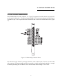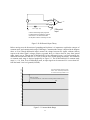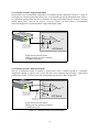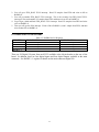
1
PCIM-DAS1602/16
ANALOG & DIGITAL I/O BOARD
for the PCI Bus
User’s Manual
Revision 2
© Copyright September, 2000
LIFETIME WARRANTY
Every hardware product manufactured by Measurement Computing Corp. is warranted against defects in
materials or workmanship for the life of the product, to the original purchaser. Any products found to be
defective will be repaired or replaced promptly.
LIFETIME HARSH ENVIRONMENT WARRANTYTM
Any Measurement Computing Corp. product which is damaged due to misuse may be replaced for only
50% of the current price. I/O boards face some harsh environments, some harsher than the boards are
designed to withstand. When that happens, just return the board with an order for its replacement at only
50% of the list price. Measurement Computing Corp. does not need to profit from your misfortune. By
the way, we will honor this warranty for any other manufacture’s board that we have a replacement for!
30 DAY MONEY-BACK GUARANTEE
Any Measurement Computing Corp. product can be returned within 30 days of purchase for a full refund
of the price paid for the product being returned. If you are not satisfied, or chose the wrong product by
mistake, you do not have to keep it. Please call for a RMA number first. No credits or returns accepted
without a copy of the original invoice. Some software products are subject to a repackaging fee.
These warranties are in lieu of all other warranties, expressed or implied, including any implied warranty
of merchantability or fitness for a particular application. The remedies provided herein are the buyer’s
sole and exclusive remedies. Neither Measurement Computing Corp., nor its employees shall be liable
for any direct or indirect, special, incidental or consequential damage arising from the use of its products,
even if Measurerment Computing Corp. has been notified in advance of the possibility of such damages.
MEGA-FIFO, the CIO prefix to data acquisition board model numbers, the PCM prefix to data acquisition board model numbers, PCM-DAS08, PCM-D24C3, PCM-DAC02, PCM-COM422, PCM-COM485,
PCM-DMM, PCM-DAS16D/12, PCM-DAS16S/12, PCM-DAS16D/16, PCM-DAS16S/16, PCIDAS6402/16, Universal Library, InstaCal, Harsh Environment Warranty and Measurement Computing
are registered trademarks of Measurement Computing Corp.
IBM, PC, and PC/AT are trademarks of International Business Machines Corp. Windows is a trademark
of Microsoft Corp. All other trademarks are the property of their respective owners.
Information furnished by Measurement Computing Corp. is believed to be accurate and reliable. However, no responsibility is assumed by Measurement Computing Corp. neither for its use; nor for any
infringements of patents or other rights of third parties, which may result from its use. No license is
granted by implication or otherwise under any patent or copyrights of Measurement Computing Corp.
All rights reserved. No part of this publication may be reproduced, stored in a retrieval system, or transmitted, in any form by any means, electronic, mechanical, by photocopying, recording or otherwise without the prior written permission of Measurement Computing Corp.
Notice
Measurement Computing Corp. does not authorize any Measurement Computing Corp. product for use
in life support systems and/or devices without the written approval of the President of Measurement
Computing Corp. Life support devices/systems are devices or systems which, a) are intended for surgical
implantation into the body, or b) support or sustain life and whose failure to perform can be reasonably
expected to result in injury. Measurement Computing Corp. products are not designed with the components required, and are not subject to the testing required to ensure a level of reliability suitable for the
treatment and diagnosis of people.
HM PCIM-DAS1602_16.lwp
Table of Contents
1 INTRODUCTION . . . . . . . . . . . . . . . . . . . . . . . . . . . . . . . . . . . . . . . . . . . . . . . . . . . . . . . . . . . . . . . 1
2. INSTALLATION & CONFIGURATION . . . . . . . . . . . . . . . . . . . . . . . . . . . . . . . . . . . . . . . . . . . . 1
2.1 BASE I/O ADDRESS & INTERRUPT LEVEL . . . . . . . . . . . . . . . . . . . . . . . . . . . . . . . . . . . . . . . 1
2.2 1/10 MHZ XTAL JUMPER . . . . . . . . . . . . . . . . . . . . . . . . . . . . . . . . . . . . . . . . . . . . . . . . . . . . . . 2
2.3 8/16 CHANNEL SELECT . . . . . . . . . . . . . . . . . . . . . . . . . . . . . . . . . . . . . . . . . . . . . . . . . . . . . . . 2
2.4 BIPOLAR/UNIPOLAR AND GAIN SETTING . . . . . . . . . . . . . . . . . . . . . . . . . . . . . . . . . . . . . . . 3
2.5 CONVERSION START, EDGE SELECT . . . . . . . . . . . . . . . . . . . . . . . . . . . . . . . . . . . . . . . . . . . 3
2.6 D/A CONVERTER REFERENCE & SSH JUMPER BLOCK . . . . . . . . . . . . . . . . . . . . . . . . . . . . 3
2.8 TESTING THE INSTALLATION . . . . . . . . . . . . . . . . . . . . . . . . . . . . . . . . . . . . . . . . . . . . . . . . . 5
2.9 CALIBRATION . . . . . . . . . . . . . . . . . . . . . . . . . . . . . . . . . . . . . . . . . . . . . . . . . . . . . . . . . . . . . . . 5
.................................................................. 6
3 SOFTWARE
3.1 CUSTOM SOFTWARE USING THE UNIVERSAL LIBRARY . . . . . . . . . . . . . . . . . . . . . . . . . 6
3.2 FULLY INTEGRATED SOFTWARE PACKAGES (E.G., SOFTWIRETM) . . . . . . . . . . . . . . . . 6
3.3 DIRECT REGISTER LEVEL PROGRAMMING . . . . . . . . . . . . . . . . . . . . . . . . . . . . . . . . . . . . . . 6
4 CONNECTOR PIN OUTS . . . . . . . . . . . . . . . . . . . . . . . . . . . . . . . . . . . . . . . . . . . . . . . . . . . . . . . . . 7
4.1 MAIN CONNECTOR DIAGRAM . . . . . . . . . . . . . . . . . . . . . . . . . . . . . . . . . . . . . . . . . . . . . . . . . 7
4.2 DIGITAL I/O CONNECTOR . . . . . . . . . . . . . . . . . . . . . . . . . . . . . . . . . . . . . . . . . . . . . . . . . . . . . 8
5 ANALOG CONNECTIONS . . . . . . . . . . . . . . . . . . . . . . . . . . . . . . . . . . . . . . . . . . . . . . . . . . . . . . . 8
5.1 ANALOG INPUTS . . . . . . . . . . . . . . . . . . . . . . . . . . . . . . . . . . . . . . . . . . . . . . . . . . . . . . . . . . . . . 9
5.1.1 Single-Ended and Differential Inputs . . . . . . . . . . . . . . . . . . . . . . . . . . . . . . . . . . . . . . . . . . . . 9
5.1.2 System Grounds and Isolation . . . . . . . . . . . . . . . . . . . . . . . . . . . . . . . . . . . . . . . . . . . . . . . . . 12
5.2 WIRING CONFIGURATIONS . . . . . . . . . . . . . . . . . . . . . . . . . . . . . . . . . . . . . . . . . . . . . . . . . . 14
5.2.1 Common Ground / Single-Ended Inputs . . . . . . . . . . . . . . . . . . . . . . . . . . . . . . . . . . . . . . . . . 15
5.2.2 Common Ground / Differential Inputs . . . . . . . . . . . . . . . . . . . . . . . . . . . . . . . . . . . . . . . . . . 15
5.2.3 Common Mode Voltage < +/-10V / Single-Ended Inputs . . . . . . . . . . . . . . . . . . . . . . . . . . . . 16
5.2.4 Common Mode Voltage < +/-10V / Differential Inputs . . . . . . . . . . . . . . . . . . . . . . . . . . . . . 16
5.2.5 Common Mode Voltage > +/-10V . . . . . . . . . . . . . . . . . . . . . . . . . . . . . . . . . . . . . . . . . . . . 16
5.2.6 Isolated Grounds / Single-Ended Inputs . . . . . . . . . . . . . . . . . . . . . . . . . . . . . . . . . . . . . . . . . 17
5.2.7 Isolated Grounds / Differential Inputs . . . . . . . . . . . . . . . . . . . . . . . . . . . . . . . . . . . . . . . . . . . 18
5.3 ANALOG OUTPUTS . . . . . . . . . . . . . . . . . . . . . . . . . . . . . . . . . . . . . . . . . . . . . . . . . . . . . . . . . . 18
6 REGISTER ARCHITECTURE . . . . . . . . . . . . . . . . . . . . . . . . . . . . . . . . . . . . . . . . . . . . . . . . . . . 20
6.1 OVERVIEW . . . . . . . . . . . . . . . . . . . . . . . . . . . . . . . . . . . . . . . . . . . . . . . . . . . . . . . . . . . . . . . . . 20
6.2 BARD1 REGISTER . . . . . . . . . . . . . . . . . . . . . . . . . . . . . . . . . . . . . . . . . . . . . . . . . . . . . . . . . . . 20
6.3 BADR2 REGISTERS . . . . . . . . . . . . . . . . . . . . . . . . . . . . . . . . . . . . . . . . . . . . . . . . . . . . . . . . . . 21
6.4 BADR3 REGISTERS . . . . . . . . . . . . . . . . . . . . . . . . . . . . . . . . . . . . . . . . . . . . . . . . . . . . . . . . . . . 23
6.5 BADR4 PORT I/O REGISTERS . . . . . . . . . . . . . . . . . . . . . . . . . . . . . . . . . . . . . . . . . . . . . . . . . 31
7 CALIBRATION AND TEST . . . . . . . . . . . . . . . . . . . . . . . . . . . . . . . . . . . . . . . . . . . . . . . . . . . . . . 34
7.1 REQUIRED EQUIPMENT . . . . . . . . . . . . . . . . . . . . . . . . . . . . . . . . . . . . . . . . . . . . . . . . . . . . . . 34
7.2 CALIBRATING THE A/D & D/A CONVERTERS . . . . . . . . . . . . . . . . . . . . . . . . . . . . . . . . . . 34
8 ANALOG ELECTRONICS . . . . . . . . . . . . . . . . . . . . . . . . . . . . . . . . . . . . . . . . . . . . . . . . . . . . . . . 35
8.1 VOLTAGE DIVIDERS . . . . . . . . . . . . . . . . . . . . . . . . . . . . . . . . . . . . . . . . . . . . . . . . . . . . . . . . . 35
8.2 LOW PASS FILTERS . . . . . . . . . . . . . . . . . . . . . . . . . . . . . . . . . . . . . . . . . . . . . . . . . . . . . . . . . . 36
9. SPECIFICATIONS . . . . . . . . . . . . . . . . . . . . . . . . . . . . . . . . . . . . . . . . . . . . . . . . . . . . . . . . . . . . 37
This page is blank.
1 INTRODUCTION
The PCIM-DAS1602/16 is a multifunction measurement and control board designed to operate in
computers with PCI bus accessory slots. The architecture of the boards is loosely based on the original
CIO-DAS16; the standard of ISA bus data acquisition. Much has changed due to improvements in
technology.
The PCIM-DAS1602/16 is easy to use. This manual will help you quickly and easily setup, install and
test your board. We assume you already know how to open the PC and install expansion boards. If you
are unfamiliar or uncomfortable with board installation, please refer to your computer’s documentation.
This manual will show you how to properly set the switches and jumpers on the board prior to
physically installing the board in your computer.
2. INSTALLATION & CONFIGURATION
The PCIM-DAS1602/16 has a number of switches and jumpers to set before installing the board in your
computer.
The board has a variety of switches and jumpers to set before installing the board in your
computer. By far the simplest way to configure your board is to use the InstaCalTM program
provided as part of your software package. InstaCalTM will show you all available options, how
to configure the various switches and jumpers to match your application requirements, and will
create a configuration file that your application software (and the Universal Library) will refer to
so the software you use will automatically know the exact configuration of the board.
Please refer to the Software Installation Manual regarding the installation and operation of
InstaCalTM. The following hard copy information is provided as a matter of completeness, and
will allow you to set the hardware configuration of the board if you do not have immediate access
to InstaCalTM and/or your computer.
2.1 BASE I/O ADDRESS & INTERRUPT LEVEL
The PCIM-DAS1602/16 uses a number of addresses (Base Address Regions or BADRs) and one
interrupt. The addresses are allocated by the PCI plug & play procedure and may not be modified. If you
have installed ISA bus boards in the past you are familiar with the need to select a base address and
interrupt level. On PCI systems it is not required to select a base address and ensure that it does not
conflict with an installed port. In PCI systems, the operating software and installation software do the
selection and checking for you.
The computer BIOS selects and sets the I/O address and interrupt level from the range of available
addresses. This address and other information is read by InstaCAL and stored in the configuration file
1
CB.CFG. This file is accessed by the Universal Library for programmers. Note also that the Universal
Library is the I/O board interface for packaged applications such as SoftWIRE, and Agilent-VEE,
therefore the InstaCal settings must be made in order for these and other applications to run.
The base address and interrupt level are also stored in the system software. Once InstaCal installation
software is run, other programming methods such as direct IN and OUT statements can write and read
the PCIM-DAS1602/16 registers by reference to the base address and the offset from base address
corresponding to the chart of registers located elsewhere in this manual.
But a word of warning is in order here. Direct writes to the addresses simply by reference to the base
address of the PCIM-DAS1602/16 I/O registers is not advised. Since the addresses assigned by the PCI
plug & play software are not under your control, there is no way to guarantee that your program will run
in any other computer.
Not only that, but if you install another PCI board in a computer after the PCIM-DAS1602/16 addresses
have been assigned, those addresses may be moved by the plug & play software when the second board is
installed. It is best to use a library such as Universal Library or a program such as SoftWIRE,
DasWizard, or Agilent-VEE to make measurements with your PCIM-DAS1602/16.
2.2 1/10 MHz XTAL JUMPER
10
The 1/10 MHz XTAL jumper selects the frequency of the square
wave used as a clock by the A/D pacer circuitry (Figure 2-1). This
pacer circuitry controls the sample timing of the A/D. The
internal pacer output driving the A/D converter is also available at
the CTR 3 Output (pin 20) on the main connector. Select 10 MHz
unless you have reason to do otherwise.
CLK SEL
1
D efault 1M H z S how n
Figure 2-1. 1 or 10 MHz Select Jumper
2.3 8/16 CHANNEL SELECT
The analog inputs of the PCIM-DAS1602/16 can be configured as
eight differential or 16 single-ended channels. Use the single-ended
input mode if you have more than eight analog inputs to sample.
Using the differential input mode allows up to 10 volts of common
mode (ground loop) rejection and will provide better noise
immunity.
CHAN
8
16
8 /1 6 C H A N N E L S E L E C T S W IT C H
The PCIM-DAS1602/16 comes from the factory configured for 16 (8 C h a n n e ls , D if fe re n tia l In p u t M o d e S h o w n )
single-ended inputs. The 8/16 switch is shown in the 8-channel
position in Figure 2-2. Set it for the type and number of inputs you
desire.
Figure 2-2. 8/16 Channel Select Switch
2
2.4 BIPOLAR/UNIPOLAR AND GAIN SETTING
The Bipolar or Unipolar configuration of the A/D converter is set by switch S2 (Figure 2-3). The switch
controls all A/D channels. Though you cannot run some channels bipolar and some unipolar, you can
measure a unipolar input in the bipolar mode. (e.g. you can monitor a 0 to 5V input with a +/-5 V
channel)
Figure 2-3. Bipolar/Unipolar Select Switch
The input amplifier gain is selectable by software.
2.5 CONVERSION START, EDGE SELECT
The original Keithley MetraByte DAS-1600 was designed such that A/D conversion was initiated on the
falling edge of the convert signal. Neither the original DAS-16, nor any of the other DAS-16 derivative
converts on the falling edge. In fact, we are not aware of any A/D board that uses the falling edge to
initiate the A/D conversion.
When using the falling edge to start the conversion, the A/D may be
falsely triggered by 8254 pacer clock initialization glitching (easy to
avoid but a real possibility in the DAS-1600). Converting on the falling
edge mode also may lead to timing differences if the
PCIM-DAS1602/16 board is being used as a replacement for an older
DAS16 series board. Because using the falling edge trigger was
undesirable, we have designed a jumper into the PCIM-DAS1602/16
which allows you choose the edge that starts the A/D conversion. The
PCIM-DAS1602/16 is shipped with this jumper in the rising edge
position.
TRIGGER EDGE SELECT
JUMPER BLOCK
Falling Edge A/D Trigger
DAS-1600 Method
P8
Rising Edge A/D Trigger
DAS-16 Method
Default
Setting
P8
Figure 2-4 to the right shows the edge selection options.
For compatibility with all third party packages, with all DAS-16
software and with PCIM-DAS1602/16 software, leave this jumper in
the rising edge position.
Figure 2-4. Trigger Edge-Select
Jumper
2.6 D/A CONVERTER REFERENCE & SSH JUMPER BLOCK
The jumper block located near the center of the PCIM-DAS1602/16 allows you to use the on board
precision voltage reference to select the output ranges of the digital to analog converters.
3
Analog output is provided by two 12-bit multiplying D/A converters. This type of converter accepts a
reference voltage and provides an output proportional to that. The proportion is controlled by the D/A
output code (0 to 4095). Each bit represents 1/4096 of full scale.
A precision −5V and −10V reference provide onboard D/A ranges of 0 to 5V, 0 to 10V, +/-5V, +/-10V.
Other ranges between 0V and 10V are available if you provide a precision voltage reference at pin 10
(D/A0) or 26 (D/A1) of the main connector.
When the DAC1 reference is supplied onboard, pin 26 of the 37-pin connector is unused and can be
employed as a SSH (simultaneous sample & hold) trigger for use with the CIO-SSH16. To do so, place
the jumper between the two pins “SH” (Figure 2-5).
Bipolar/Unipolar Select Jumpers
D/A0 & D/A1 Range Jumper Block
Figure 2-5. D/A Bipolar/Unipolar Select & Output Range Jumpers
4
2.8 TESTING THE INSTALLATION
After you have run the install program, it is time to test the installation. The following section describes
the InstaCal procedure to test that your board is properly installed. The procedure has you connect one of
the output channels to one of the A/D channels, it then outputs a simple waveform and shows you the
waveform monitored on the selected A/D channel.
1. With InstaCal running, select the PCIM-DAS1602/16.
2. Select the "TEST" function from the main menu
3. Follow the instructions provided
If you do not receive the expected results:
a. make certain you have connected the correct pins according to the connector diagram.
b. go back through the installation procedure and make sure you have installed the
board according to the instructions.
If this does not get you to the desired display, please call us (or contact your local distributor) for
additional assistance.
2.9 Calibration
Selecting CALIBRATE from the InstaCal main menu runs a fully automated PCIM-DAS1602/16
calibration program. The software controlled calibration of the PCIM-DAS1602/16 is explained further
in the section on calibration.
5
3 SOFTWARE
There are three common approaches for generating operating software for the PCIM-DAS1602/16.
These are:
Writing custom software with our Universal Library package,
Using a fully integrated software package such as SoftWIRE, or
Doing direct, register-level programming.
3.1 CUSTOM SOFTWARE USING THE UNIVERSAL LIBRARY
Some users write custom software using our Universal Library. The Universal Library takes care of all
the board I/O commands and lets you concentrate on the application part of the software. For additional
information regarding using the Universal Library, please refer to the documentation supplied with the
Universal Library package.
3.2 FULLY INTEGRATED SOFTWARE PACKAGES (e.g., SoftWIRETM)
Many users now take advantage of the power and simplicity offered by an the upper-level data
acquisition package such as SoftWIRE or DasWizard.
SoftWIRE is a new, easy-to-use graphical programming package that runs in Visual Basic.
Non-programmers can build powerful applications without writing any code. Experienced programmers
can easily integrate a new application with existing software with a minimum of effort. Please refer to
the package’s documentation for setup and complete usage information.
3.3 DIRECT REGISTER LEVEL PROGRAMMING
Although uncommon, some applications do not allow the use of our Universal Library. If the user does
not desire to use a new, simplified, upper-level package such as SoftWIRE, we include detailed, register
mapping information in Chapter 6.
6
4 CONNECTOR PIN OUTS
4.1 MAIN CONNECTOR DIAGRAM
The PCIM-DAS1602/16 analog connector is a 37-pin “D” connector accessible from the rear of the PC
on the expansion back plate. An additional signal, SS&H OUT (Simultaneous Sample and Hold Output),
is available at pin 26. It is required when the CIO-SSH16 card is used with a PCIM-DAS1602/16 (Figure
4-1).
Figure 4-1. Main Analog Connector Pinout
The connector accepts female 37-pin D-type connectors, such as those on the C73FF-2, a two-foot cable
with connectors. If frequent changes to signal connections or signal conditioning is required we strongly
recommend purchasing the CIO-MINI37 screw terminal board and the mating C37FF-2 cable
7
4.2 DIGITAL I/O CONNECTOR
The digital I/O connector is mounted at the rear of the PCIM-DAS1602/16 and will accept a 40-pin
header connector. The optional BP40-37 cable assembly brings the signals to a back plate with a 37-pin
male connector mounted in it. When connected through the BP40-37, the PCIM-DAS1602/16 digital
connector is identical to the CIO-DIO24 connector. The pinouts of the 40-pin digital I/O connector and
BP40-37 cable are shown in Figure 4-2 below. (They are repeated in the Specifications section.)
GND
+ 5V
GND
NC
GND
NC
GND
NC
GND
PORT B 0
PORT B 1
PORT B 2
PORT B 3
PORT B 4
PORT B 5
PORT B 6
PORT B 7
NC
NC
Figure 4-2. - Digital I/O Connector Pinout
8
19
18
17
16
15
14
13
12
11
10
9
8
7
6
5
4
3
2
1
37
36
35
34
33
32
31
30
29
28
27
26
25
24
23
22
21
20
PORT
PORT
PORT
PORT
PORT
PORT
PORT
PORT
PORT
PORT
PORT
PORT
PORT
PORT
PORT
PORT
GND
+ 5V
BP40-37 Cable Pinout
A
A
A
A
A
A
A
A
C
C
C
C
C
C
C
C
0
1
2
3
4
5
6
7
0
1
2
3
4
5
6
7
5 ANALOG CONNECTIONS
5.1 ANALOG INPUTS
Analog signal connection is one of the most challenging aspects of applying a data acquisition board. If
you are an Analog Electrical Engineer then this section is not for you, but if you are like most PC data
acquisition users, the best way to connect your analog inputs may not be obvious. Though complete
coverage of this topic is well beyond the scope of this manual, the following section provides some
explanations and helpful hints regarding these analog input connections. This section is designed to help
you achieve the optimum performance from your PCIM-DAS1602/16 board.
Prior to jumping into actual connection schemes, you should have at least a basic understanding of
Single-Ended/Differential inputs and system grounding/isolation. If you are already comfortable with
these concepts you may wish to skip to the next section (on wiring configurations).
5.1.1 Single-Ended and Differential Inputs
The PCIM-DAS1602/16 provides either eight differential or 16 single-ended input channels.
Single-Ended Inputs
A single-ended input measures the voltage between the input signal and ground. In this case, in
single-ended mode the PCIM-DAS1602/16 measures the voltage between the input channel and LLGND.
The single-ended input configuration requires only one physical connection (wire) per channel and
allows the PCIM-DAS1602/16 to monitor more channels than the (2-wire) differential configuration
using the same connector and onboard multiplexor. However, since the PCIM-DAS1602/16 is measuring
the input voltage relative to its own low level ground, single-ended inputs are more susceptible to both
EMI (Electro-Magnetic Interference) and any ground noise at the signal source. Figure 5-1a and 5-1b
show the theory of single-ended input configuration
C H IN
+
In p ut
Amp
LL G N D
To A /D
-
I/O
C o n n e c tor
S ingle-Ended Input
Figure 5-1a. Single-Ended Voltage Input Theory
9
C H IN
~
+
V s + V g2 - Vg 1
Vs
LL G ND
Inp ut
Amp
To A /D
-
g2
g1
A n y v olta ge differe ntial be tw een ground s
g1 an d g2 sho w s up a s a n error sig nal
at the inp ut am plifier
S in gle -e n de d inp ut w ith C o m m o n M od e Volta g e
Figure 5-1b. Single-Ended Voltage Input Theory
Differential Inputs
Differential inputs measure the voltage between two distinct input signals. Within a certain range
(referred to as the common mode range), the measurement is almost independent of signal source to
PCIM-DAS1602/16 ground variations. A differential input is also much more immune to EMI than a
single-ended one. Most EMI noise induced in one lead is also induced in the other, the input only
measures the difference between the two leads, and the EMI common to both is ignored. This effect is a
major reason there is twisted pair wire as the twisting assures that both wires are subject to virtually
identical external influence. Figure 5-2a and 5-2b below show a typical differential input configuration.
CH H igh
+
Inp ut
Amp
CH L ow
To A /D
-
LL GN D
I/O
C o nn ector
D ifferential Inpu t
Figure 5-2a . Differential Input Theory
10
~
CH High
Vs
CH Low
Vcm
g1
+
Vs
Vcm = Vg2 - Vg1
Inp ut
Amp
To A/D
-
LL G ND
g2
Com m on M ode Voltage (Vcm ) is ignored
by differential input configuration. However,
note that Vcm + Vs must rem ain w ithin
the am plifier’s comm on m ode range of ±10V
D ifferential
Input
Figure 5-2b. Differential Input Theory
Before moving on to the discussion of grounding and isolation, it is important to explain the concepts of
common mode, and common mode range (CM Range). Common mode voltage is depicted in the diagram
above as Vcm. Though differential inputs measure the voltage between two signals, without (almost)
respect to the either signal’s voltages relative to ground, there is a limit to how far away from ground
either signal can go. Though the PCIM-DAS1602/16 has differential inputs, it will not measure the
difference between 100V and 101V as 1 Volt (in fact the 100V would destroy the board!). This limitation
or common mode range is depicted graphically in Figure 5-3. The PCIM-DAS1602/16 common mode
range is +/- 10 Volts. Even in differential mode, no input signal can be measured if it is more than 10V
from the board’s low level ground (LLGND).
+13V
Gray area represents com m on m ode ran
Both V+ and V- m ust alw ays rem ain w ithi
the com m on m ode range relative to LL G
+12V
+11V
+10V
+9V
+8V
+7V
W ith Vcm = +5VD C,
+Vs m ust be less than +5V, or the com m on m ode range will be exceeded (>+10V)
+6V
Vcm
+5V
+4V
+3V
+2V
+1V
-1V
-2V
-3V
-4V
-5V
-6V
-7V
-8V
-9V
-10V
11V
Figure 5-3. Common Mode Range
11
5.1.2 System Grounds and Isolation
There are three scenarios possible when connecting your signal source to your PCIM-DAS1602/16
board.
1. The PCIM-DAS1602/16 and the signal source have the same (or common) ground. This signal
source can be connected directly to the PCIM-DAS1602/16.
2. The PCIM-DAS1602/16 and the signal source have an offset voltage between their grounds (AC
and/or DC). This offset it commonly referred to a common mode voltage. Depending on the
magnitude of
this voltage, it may or may not be possible to connect the PCIM-DAS1602/16
directly to your signal source. We will discuss this topic further in a later section.
3. The PCIM-DAS1602/16 and the signal source already have isolated grounds. This signal source
can be connected directly to the PCIM-DAS1602/16.
Which system do you have?
Try the following experiment. Using a battery powered voltmeter*, measure the voltage (difference)
between the ground signal at your signal source and at your PC. Place one voltmeter probe on the PC
ground and the other on the signal source ground. Measure both the AC and DC Voltages.
*If you do not have access to a voltmeter, skip the experiment and take a look a the following three
sections. You may be able to identify your system type from the descriptions provided.
If both AC and DC readings are 0.00 volts, you may have a system with common grounds. However,
since voltmeters will average out high frequency signals, there is no guarantee. Please refer to the section
below titled Common Grounds.
If you measure reasonably stable AC and DC voltages, your system has an offset voltage between the
grounds category. This offset is referred to as a Common Mode Voltage. Please be careful to read the
following warning and then proceed to the section describing Common Mode systems.
WARNING
If either the AC or DC voltage is greater than 10 volts, do not connect the
PCIM-DAS1602/16 to this signal source. You are beyond the boards usable common
mode range and will need to either adjust your grounding system or add special
Isolation signal conditioning to take useful measurements. A ground offset voltage of
more than 30 volts will likely damage the PCIM-DAS1602/16 board and possibly your
computer. Note that an offset voltage much greater than 30 volts will not only damage
your electronics, but it can also be hazardous to your health.
This is such an important point, that we will state it again. If the voltage between the
ground of your signal source and your PC is greater than 10 volts, your board will not
take useful measurements. If this voltage is greater than 30 volts, it will likely cause
damage, and can represent a serious shock hazard! In this case you will need to either
reconfigure your system to reduce the ground differentials, or purchase and install
special electrical isolation signal conditioning.
12
If you cannot obtain a reasonably stable DC voltage measurement between the grounds, or the voltage
drifts around considerably, the two grounds are most likely isolated. The easiest way to check for
isolation is to change your voltmeter to it’s ohm scale and measure the resistance between the two
grounds. It is recommended that you turn both systems off prior to taking this resistance measurement. If
the measured resistance is more than 100 Kohm, it’s a fairly safe bet that your system has electrically
isolated grounds.
Systems with Common Grounds
In the simplest (but perhaps least likely) case, your signal source will have the same ground as the
PCIM-DAS1602/16. This would typically occur when providing power or excitation to your signal
source directly from the PCIM-DAS1602/16. There may be other common ground configurations, but it
is important to note that any voltage between the PCIM-DAS1602/16 ground and your signal ground is a
potential error voltage if you set up your system based on a common ground assumption.
As a safe rule of thumb, if your signal source or sensor is not connected directly to an LLGND pin on
your PCIM-DAS1602/16, it’s best to assume that you do not have a common ground even if your
voltmeter measured 0.0 Volts. Configure your system as if there is ground offset voltage between the
source and the PCIM-DAS1602/16. This is especially true if you are using the PCIM-DAS1602/16 at
high gains since ground potentials in the sub-millivolt range will be large enough to cause A/D errors, yet
will not likely be measured by your hand-held voltmeter.
Systems with Common Mode (ground offset) Voltages
The most frequently encountered grounding scenario involves grounds that are somehow connected, but
have AC and/or DC offset voltages between the PCIM-DAS1602/16 and signal source grounds. This
offset voltage may be AC, DC or both and can be caused by a wide array of phenomena including EMI
pickup, resistive voltage drops in ground wiring and connections, etc. Ground offset voltage is a more
appropriate term to describe this type of system, but since our goal is to keep things simple, and help you
make appropriate connections, we’ll stick with our somewhat loose usage of the phrase Common Mode.
Small Common Mode Voltages
If the voltage between the signal source ground and PCIM-DAS1602/16 ground is small, the combination
of the ground voltage and input signal will not exceed the +/-10V common mode range, (i.e. the voltage
between grounds, added to the maximum input voltage, stays within +/-10V), This input is compatible
with the PCIM-DAS1602/16 and the system can be connected without additional signal conditioning.
Fortunately, most systems will fall in this category and have a small voltage differential between
grounds.
Large Common Mode Voltages
If the ground differential is large enough, the +/- 10V common mode range can be exceeded. (If the
voltage between the card and signal source ground, plus the maximum input voltage you’re trying to
measure, if this exceeds +/-10V, you’ll exceed the maximum CMR.) In this case the PCIM-DAS1602/16
cannot be directly connected to the signal source. You will need to change your system grounding
configuration or add isolation signal conditioning. (Please look at our ISO-RACK and ISO-5B-series
products to add electrical isolation, or give our technical support group a call to discuss other options.)
13
NOTE
Relying on the earth prong of a 120VAC for signal ground connections is not advised..
Different ground plugs may have large and potentially even dangerous voltage
differentials. Remember that the ground pins on 120VAC outlets on different sides of the
room may only be connected in the basement. This leaves the possibility that the
“ground” pins may have a significant voltage differential (especially if the two 120VAC
outlets happen to be on different phases.)
PCIM-DAS1602/16 and signal source already have isolated grounds
Some signal sources will already be electrically isolated from the PCIM-DAS1602/16. The diagram
below shows a typical isolated ground system. These signal sources are often battery powered, or are
fairly expensive pieces of equipment (since isolation is not an inexpensive proposition), isolated ground
systems provide excellent performance, but require some extra effort during connections to assure
optimum performance is obtained. Please refer to the following sections for further details.
5.2 WIRING CONFIGURATIONS
Combining all the grounding and input type possibilities provides us with the following potential
connection configurations. The combinations along with our recommendations on usage are shown in
Table 5-1 below.
Table 5-1. Input vs. Grounding Recommendations
Ground Category
Input Configuration
Our Recommendation
Common Ground
Single-Ended Inputs
Recommended
Common Ground
Differential Inputs
Acceptable
Common Mode
Voltage < +/-10V
Single-Ended Inputs
Not Recommended
Common Mode
Voltage < +/-10V
Differential Inputs
Recommended
Common Mode
Voltage > +/- 10V
Single-Ended Inputs
Unacceptable without
adding Isolation
Common Mode
Voltage > +/-10V
Differential Inputs
Unacceptable without
adding Isolation
Already Isolated Grounds
Single-ended Inputs
Acceptable
Already Isolated
Grounds
Differential Inputs
Recommended
The following sections depicts recommended input wiring schemes for each of the eight possible input
configuration/grounding combinations.
14
5.2.1 Common Ground / Single-Ended Inputs
Single-ended is the recommended configuration for common ground connections. However, if some of
your inputs are common ground and some are not, we recommend you use the differential mode. There is
no performance penalty (other than loss of channels) for using a differential input to measure a common
ground signal source. However the reverse is not true. Figure 5-4 below shows a recommended
connection diagram for a common ground / single-ended input system
l
S ig n a rc e w it h
d
Sou
on Gn
Comm
C H IN
+
LL G N D
O p tio nal w ire
since signa l sou rce
and A /D bo ard sh are
com m on g round
In p ut
Amp
To A /D
-
I/O
C o n n ec tor
A /D B o a rd
S ignal source an d A /D board
sharing com m o n grou nd con nected
to single-ended inp ut.
Figure 5-4. Common Ground / Single-Ended Inputs
5.2.2 Common Ground / Differential Inputs
The use of differential inputs to monitor a signal source with a common ground is a acceptable
configuration though it requires more wiring and offers fewer channels than selecting a single-ended
configuration. Figure 5-5 below shows the recommended connections in this configuration.
l
S ig n a rc e w it h
d
Sou
on Gn
Comm
C H H igh
+
Inp ut
Amp
C H L ow
O p tio nal w ire
since signa l sou rce
and A/D bo ard sha re
com m o n g round
To A /D
-
LL G N D
I/O
C o nn ec tor
A /D B o a rd
R equ ired connection
of L L G N D to C H Low
S igna l source and A /D board
sha ring com m on ground connected
to differential input.
Figure 5-5. Common Ground / Differential Inputs
15
5.2.3 Common Mode Voltage < +/-10V / Single-Ended Inputs
This is not a recommended configuration. In fact, the phrase common mode has no meaning in a
single-ended system and this case would be better described as a system with offset grounds. You can try
this configuration, no system damage should occur and you may receive acceptable results.
5.2.4 Common Mode Voltage < +/-10V / Differential Inputs
Systems with varying ground potentials should always be monitored in the differential mode. Care is
required to assure that the sum of the input signal and the ground differential (referred to as the common
mode voltage) does not exceed the common mode range of the A/D board (+/-10V on the
PCIM-DAS1602/16). Figure 5-6 below show recommended connections in this configuration.
S ig n a
e
l S o u rc o m m o n
w it h C d e V o lt a g e
Mo
GND
C H H igh
+
Inp ut
Amp
C H L ow
To A /D
-
LL G N D
T he vo lta g e differen tia l
b etw een the se g ro un d s,
a dde d to the m ax im u m
in pu t sig na l m ust sta y
w ith in + /-10 V
I/O
C o nn ec tor
A /D B o a rd
S igna l source a nd A /D board
w ith com m on m ode volta ge
conn ected to a differential input.
Figure 5-6. Common Mode Voltage < +/-10V / Differential Inputs
5.2.5 Common Mode Voltage > +/-10V
The PCIM-DAS1602/16 will not directly monitor signals with common mode voltages greater than
+/-10V. You will either need to alter the system ground configuration to reduce the overall common
mode voltage, or add isolated signal conditioning between the source and your board. See Figure 5-7 and
5-8 below.
Iso lation
B arrie r
com m
on
L a rg e d e v o lt a g e ig n a l
mo
een s
b o a rd
b e tw rc e & A /D
sou
GND
C H IN
+
Inp ut
Amp
LL G N D
To A /D
-
I/O
C o nn ector
W h en the voltage difference
betw een sign al source and
A /D boa rd gro und is large
enough so the A /D board’s
com m on m ode ran ge is
exceede d, is olated sig nal
conditioning m ust be added.
A /D B o a rd
S ystem w ith a Large C om m on M ode Voltage,
C onne cte d to a Single-Ended Input
Figure 5-7. Common Mode Voltage > +/-10V. Single-Ended Input
16
Iso latio n
B arrie r
on
co m m
L ar ge od e vo lta ge gn al
m
n si
bo ar d
be tw eeur ce & A /D
so
GND
C H H igh
+
In p u t
Amp
C H Low
To A /D
-
10 K
LL G N D
W hen the voltage difference
betw een signal source and
A /D board ground is large
enough so the A /D board’s
com m on m ode range is
exceeded, isolated signal
conditioning m ust be added.
I/O
C o nn ec tor
A /D B o a rd
1 0 K is a re c o m m e n d e d v a lu e . Yo u m a y s h o rt L L G N D to C H L ow
in s te ad , b ut th is w ill re d u c e y o u r s y s tem ’s n o ise im m u nity.
S ystem w ith a La rge C om m on M ode Voltag e,
C onne cte d to a D ifferential Inp ut
Figure 5-8. Common Mode Voltage > +/-10V. Differential Input
5.2.6 Isolated Grounds / Single-Ended Inputs
Single-ended inputs can be used to monitor isolated inputs, though the use of the differential mode will
increase you system’s noise immunity. Figure 5-9 below shows the recommended connections is this
configuration.
d
Is o la te ig n a l
s
e
s o u rc
CH IN
+
Inp ut
Amp
LL GND
To A /D
-
I/O
C o nn ector
A /D B o ard
Iso lated S ignal S ource
C onne cte d to a S ingle-E nded Input
Figure 5-9. Isolated Grounds / Single-Ended Input
17
5.2.7 Isolated Grounds / Differential Inputs
Optimum performance with isolated signal sources is assured with the use of the differential input
setting. Figure 5-10 below shows the recommend connections is this configuration.
e
l S o u rc
a rd
S ig n a n d A /D B o o la te d .
a
y Is
d
a
e
lr
A
GND
C H H igh
+
Inp ut
Amp
C H L ow
To A /D
-
10 K
LL G N D
I/O
C o nn ec tor
T he se g ro u n ds are
e lec trica lly isolated .
A /D B o a rd
1 0 K is a rec o m m e nd e d v a lue . Yo u m ay s ho rt LL G N D to C H L ow
in s te a d , b ut this w ill re du c e yo ur s y s tem ’s n o ise im m u nity.
A lready isolated signal source
and A /D b oard connected to
a differential in pu t.
Figure 5-10. Isolated Grounds / Differential Inputs
5.3 ANALOG OUTPUTS
Analog outputs are simple voltage outputs which can be connected to any device which will record,
display or be controlled by a voltage. The PCIM-DAS1602/16 analog outputs are 4 quadrant multiplying
DACs. This means that they accept an input voltage reference and provide an output voltage which is
inverse to the reference voltage and proportional to the digital value in the output register.
For example, in unipolar mode, the supplied reference of −5V provides a +5V output (actually 4.9988V)
when the value in the output register is 4095 (full scale at 12 bits of resolution). It provides a value of
2.5V when the value in the output register is 2048.
Figure 5-11 shows the onboard reference internally jumpered. Both D/A outputs will have a range of
−5 to +5 volts. This is the default factory configuration.
18
Bipolar/Unipolar Select Jumpers
D/A0 & D/A1 Range Jumper Block
Figure 5-11. Analog Output Range Select Jumper Block
19
6 REGISTER ARCHITECTURE
6.1 OVERVIEW
PCIM-DAS1602/16 operation registers are mapped into I/O space. Unlike ISA bus designs, this
board has several base address regions, each corresponding to a reserved block of addresses in
I/O space. Of the six Base Address Regions (BADRs) available per the PCI 2.1 specification,
five are implemented in this design and are summarized in Table 6-1 as follows.
I/O Region
BADR0
BADR1
BADR2
BADR3
BADR4
Table 6-1. PCIM-DAS1602/16 BADR Mapping
Function
Operations
PCI memory mapped configuration registers
32-bit Double Word
PCI I/O mapped configuration registers
32-bit Double Word
ADC and DAC data registers
16-bit Word
Pacer, Counter, Trigger, Interrupt, and
8-bit Byte
Digital I/O configuration registers
82C55 Digital I/O registers
8-bit Byte
BADRn will likely be different on different machines. Assigned by the PCI BIOS, these Base Address
values cannot be guaranteed to be the same even on subsequent power-on cycles of the same machine.
All software must interrogate BADR0 at run-time with a READ_CONFIGURATION_DWORD
instruction to determine the BADRn values.
BADR0 and BADR1 are used for PCI configuration. Only the PCI Interrupt Control/Status Register
(BADR1 + 4Ch) should be used. All others should not be written to. This Board uses the PLX PCI9052
PCI Bus Interface chip. For additional information on BADR0 and BADR1, refer to the data sheet.
NOTE: All unused bits are denoted by an X. They are 0 for a read operation and don’t cares for a write
operation.
6.2 BARD1 REGISTER
REGISTER
BADR1 + 4Ch
BADR1+4Ch
READ/WRITE
31:7
6
0
PCINTE
READ FUNCTION
INTERRUPT STATUS
5
0
WRITE FUNCTION
INTERRUPT CONTROL
4
0
3
0
2
INT
1
1
0
LINTE
This register controls the interrupt features of the PLX-9052. For proper operation, the predefined bits,
bit 1 = 1 and bits 3, 4, 5, 7 to 31 = 0, must not be changed.
20
LINTE = 1, on the local side interrupt is enabled
LINTE = 0, on the local side interrupt is disabled
the INT bit is read only
INT = 1, interrupt is active
INT = 0, interrupt is not active
PCINTE = 1, on the PCI side, the interrupt is enabled
PCINTE = 0, on the PCI side, the interrupt is disabled
You must set both PCINTE and LINTE to 1 to enable interrupts. There is also an interrupt enable bit
(INTE) in BADR3+4. This bit must also be set to 1 to enable interrupts.
This register is only used to enable the local and PCI interrupt bits so the interrupt generated by the on
board logic can propagate through the PCI-9052 interface to the PCI bus INTA. The interrupts are not
cleared in this register. The board has both edge and level sensitive interrupts. The edge sensitive
interrupts, EndOfAcquisition, EndOfBurst, and EndOfConversion must be cleared by writing a 0 to the
INT bit in BADR3+4. This must be done at the end of your interrupt service routine. The level sensitive
interrupts, FifoHalfFull and FifoNotEmpty, will be regenerated after you service the interrupt if their
condition is still true. See the section on BADR3+4 for more details.
6.3 BADR2 REGISTERS
READ FUNCTION
ADC Data
none
none
REGISTER
BADR2 + 0
BADR2 + 2
BADR2 + 4
WRITE FUNCTION
Begin single conversion
DAC 0 Data
DAC 1 Data
The I/O Region defined by BADR2 contains the 16-bit ADC data and the two 12-bit DAC data registers.
BADR2 + 0
ADC Data/Convert.
READ
15
14
AD15
AD14
13
12
11
10
9
8
7
6
5
4
3
2
1
0
AD13
AD12
AD11
AD10
AD9
AD8
AD7
AD6
AD5
AD4
AD3
AD2
AD1
AD0
MSB
LSB
AD[15:0]
This register contains the current ADC data word. Data format is dependent upon offset mode:
Bipolar Mode: Offset Binary Coding
0000 h = −FS
7FFFh = Mid-scale (0V)
FFFFh = +FS − 1LSB
21
Unipolar Mode: Straight Binary Coding
0000 h = −FS (0V)
7FFFh = Mid-scale (+FS/2)
FFFFh = +FS − 1LSB
WRITE
Writing to this register is only valid for SW initiated conversions. The ADC Pacer source must
be set to software polled (see BADR3 + 5). A null write to BADR2 + 0 will begin a single conversion.
Conversion status may be determined by polling the EOC bit in BADR3 + 2.
BADR2 + 2
DAC 0 Data
WRITE ONLY
15
14
13
x
x
x
12
11
10
9
8
7
6
5
4
3
2
1
0
x
DA11
DA10
DA9
DA8
DA7
DA6
DA5
DA4
DA3
DA2
DA1
DA0
MSB
LSB
BADR2 + 4
DAC 1 Data
WRITE ONLY
15
14
13
x
x
x
12
11
10
9
8
7
6
5
4
3
2
1
x
DA11
DA10
DA9
DA8
DA7
DA6
DA5
DA4
DA3
DA2
DA1
MSB
0
DA0
LSB
DA[11:0]
These bits represent the DAC data word. Format is dependent upon offset mode as described below:
+/-10V Range, Vref = −10V
+/-5V Range, Vref = −5V
Bipolar Mode: Offset Binary Coding
000 h = Vref
7FFh = Mid-scale (0V)
FFFh = −Vref − 1 LSB, Vref <0V
= −Vref + 1 LSB, Vref >0V
Unipolar Mode: Straight Binary Coding
000 h = 0V
7FFh = Mid-scale (−Vref/2)
FFFh = −Vref − 1 LSB, Vref <0V
= −Vref + 1 LSB, Vref >0V
On power up and system reset, the DACs’ outputs are disabled and set to 0V. The first write to each
DAC will enable that DAC.
The DACs ranges are jumper-settable in hardware. The settings are not software-readable.
22
6.4 BADR3 REGISTERS
REGISTER
BADR3 + 0
BADR3 + 1
BADR3 + 2
BADR3 + 3
BADR3 + 4
BADR3 + 5
BADR3 + 6
BADR3 + 7
BADR3 + 8
BADR3 + 9
BADR3 + 0Ah
BADR3 + 0Bh
BADR3 + 0Ch
BADR3 + 0Dh
BADR3 + 0Eh
READ FUNCTION
Mux scan limits
Main Connector Digital Inputs
ADC Channel Status and Switch Settings
ADC Conversion Status
Interrupt Settings /Status
A/D Pacer Clock Settings
Burst Mode and Converter Settings
Programmable Gain Settings
82C54 Counter 1 Data
82C54 Counter 2 Data
82C54 Counter 3 Data
82C54 Counter Control Data
User Counter Clock Setting
MUX SCAN LIMITS REGISTER
BADR3 + 0
READ/WRITE
7
6
5
CH H3
CH H2
CH H1
4
CH H0
3
CH L3
WRITE FUNCTION
Mux scan limits
Main Connector Digital Outputs
Interrupt Control
A/D Pacer Clock Control
Burst Mode and Converter Control
Programmable Gain Control
82C54 Counter 1 Data
82C54 Counter 2 Data
82C54 Counter 3 Data
82C54 Counter Control Data
User Counter Clock Control
Residual Counter upper 2 bits
Residual Counter lower byte
2
CH L2
1
CH L1
0
CH L0
READ
The current channel scan limits are read as one byte. The high channel number scan limit is in the most
significant four bits. The low channel scan limit is in the least significant four bits.
WRITE
The channel scan limits desired are written as one byte. The high channel number scan limit is in the
most significant four bits. The low channel scan limit is in the least significant four bits.
Every write to this register sets the current A/D channel MUX setting to the number in
bits 0-3 and resets the FIFO. You should delay 10 µs after setting the MUX (to allow for
settling time) before initiating a conversion.
23
MAIN CONNECTOR DIGITAL I/O REGISTER
BADR3 + 1
READ
7
6
0
0
5
4
3
2
1
0
0
0
DI3
DI2, CTR0 GATE
DI1
DI0, EXT TRIG, EXT PACER, EXT GATE
The signals present at the inputs are read as one byte, the most significant 4 bits of which are always
zero. Digital Inputs 2 and 0 have multiple functions. Digital Input 2 may also be used as the gate to
Counter 1 of the 82C54 which is available on the Main connector, please see BADR3+6 for a more
detailed description. Digital Input 0 may also be used as either a trigger, a pacer, or a gate for the ADC,
please see BADR3+5 for a more details.
WRITE
7
X
6
X
5
X
4
X
3
DO3
2
DO2
1
DO1
0
DO0
The upper four bits are ignored. The lower four bits are latched TTL outputs. Once written, the state of
the inputs cannot be read back because a read back would read the separate digital input lines (see
above).
NOTE The digital lines 0-3, pins 3, 4, 5, 6, 22, 23, 24, & 25 of the analog connector
should not be used as ON/OFF Digital I/O. See below.
The digital inputs have multiple functions as described above. The digital outputs are also used by the
CIO-EXP32, 32 channel analog multiplexor/amplifier. There is a 24-line 82C55 on general purpose
digital I/O, see BADR4. We suggest that the Main connector 4-bit ports be kept free for analog
multiplexing control lines.
ADC CHANNEL STATUS AND SWITCH SETTINGS REGISTERS
BADR3 + 2
READ ONLY
7
EOC
6
U/B
5
MUX
4
CLK
3
MA3
2
MA2
1
MA1
EOC = 1, the A/D converter is busy.
EOC = 0, it is free.
EOC is in both BADR3+2 and BADR3+3 for convenience in software programming.
U/B = 1, the Analog Input Polarity Switch is set to Unipolar.
U/B = 0, the Analog Input Polarity Switch is set to Bipolar
MUX = 1, the Analog Input Mode Switch is set to 16 single-ended.
MUX = 0, the Analog Input Mode Switch is set to 8 differential.
CLK = 1, the Pacer Clock Jumper is set to 10 MHz
CLK = 0, the Pacer Clock Jumper is set to 1 MHz.
24
0
MA0
MA3, MA2, MA1, and MA0 is a binary number between 0 and 15 indicating the MUX channel currently
selected and is valid only when EOC = 0. The channel MUX increments shortly after EOC = 1 so may
be in a state of transition when EOC = 1.
ADC CONVERSION STATUS REGISTER
BADR3 + 3
READ ONLY
7
6
5
4
EOC
EOB
EOA
FNE
3
FHF
2
OVERRUN
1
0
0
0
EOC = 1, the A/D converter is busy.
EOC = 0, it is free.
EOC is in both BADR3+2 and BADR3+3 for convenience in software programming.
EOB = 1, An ADC Burst has been completed
EOB = 0, An ADC Burst is in progress or has not started
EOA = 1, the residual # of samples have been written to the FIFO
EOA = 0, the residual # of samples have not been written to the FIFO
EOA is cleared by writing a 0 to the INT bit in BADR3+4. See below.
EOA is in both BADR3+3 and BADR3+4 for convenience in software programming
FNE = 1, FIFO memory contains at least on sample.
FNE = 0, FIFO memory contains no samples
FHF = 1, FIFO memory contains at least 512 samples.
FHF = 0, FIFO memory contains less than 512 samples
OVERRUN = 1, FIFO memory has overrun
OVERRUN = 0, FIFO memory has not overrun
OVERRUN is in both BADR3+3 and BADR3+4 for convenience in software programming
INTERRUPT STATUS AND CONTROL
BADR3 + 4
READ/WRITE
7
6
5
4
INTE
INT
X
OVERRUN
3
EOA
2
EOA_INT_SEL
INTSEL[1:0] are used to select the source of the interrupt.
acquisition, you can only select one interrupt source.
INTSEL
1
0
0
1
1
INTSEL
0
0
1
0
1
25
0
INTSEL0
With the exception of EOA, end of
INTERRUPT SOURCE
EOC, End of Conversion
FIFO not empty
EOB, End of Burst
FIFO half full/EOA
1
INTSEL1
EOA_INT_SEL = 1, Interrupt on end of acquisition
EOA_INT_SEL = 0, No interrupt on end of acquisition
EOA_INT_SEL is used in conjunction with the residual counter. See BADR3+ 0Dh
EOA = 1, the residual # of samples have been written to the FIFO
EOA = 0, the residual # of samples have not been written to the FIFO
EOA is cleared by writing a 0 to the INT bit. See below.
EOA is in both BADR3+3 and BADR3+4 for convenience in software programming
OVERRUN = 1, FIFO memory has overrun
OVERRUN = 0, FIFO memory has not overrun
OVERRUN is in both BADR3+3 and BADR3+4 for convenience in software programming
INT = 1, Interrupt generated
INT = 0, No interrupt generated
INT must be cleared after each edge sensitive interrupt (EOC, EOB, and EOA) by setting it to 0.
INTE = 1, Interrupts are enabled.
INTE = 0, Interrupts are disabled.
To enable interrupts you must also set bits in BADR1 + 4Ch
A/D PACER CLOCK STATUS AND CONTROL
BADR3 + 5
READ/WRITE
7
X
6
GATE_STATUS
5
GATE_POL
4
GATE_LATCH
3
GATE_EN
2
EXT_PACER_POL
1
PS1
0
PS0
PS[1:0] control the source of the A/D Pacing according to the table below.
PS1
0
1
1
PS0
X
0
1
Software polled A/D
External Pacer Clock (Digital input 0, Pin 25)
Internal Pacer Clock (CTR 2 OUT, no external access)
EXT_PACER_POL = 1, the external pacer polarity is set to negative edge for non burst mode and burst
mode
EXT_PACER_POL = 0, the external pacer polarity is set to positive edge for non-burst mode and burst
mode
This bit is only used when the external pacer clock is selected. We recommend setting to positive edge.
The remainder of the bits are only used when the internal pacer is selected.
Note: The polarity (direction) of the internal pacer is set by a hardware jumper. It is recommended that
it be set to a positive-going edge.
GATE_EN = 1, the gate to the internal pacer is always on regardless of the signal on pin 25. In this
mode, the bits below are ignored.
GATE_EN = 0, the gate to the internal pacer is controlled by the signal on pin 25.
GATE_ LATCH = 1, the signal on pin 25 will act as an edge trigger to the internal pacer. It is latched in
hardware. Software must clear latch by writing a “0” to the GATE_STATUS bit.
GATE_ LATCH = 0, the signal on pin 25 will act as a level gate to the internal pacer.
26
GATE_POL = 1, the trigger / gate polarity is set to negative-going edge / low level for non burst mode
and positive-going edge / high level for burst mode
GATE_POL = 0, the trigger / gate polarity is set to positive-going edge / high level for non burst mode
and negative-going edge / low level for burst mode
on a read,
GATE_STATUS = 1, the gate to the internal pacer is on.
GATE_STATUS = 0, the gate to the internal pacer is off.
on a write,
GATE_STATUS = 0 clears the hardware latch when LATCH = 1
BURST MODE and CONVERTER CONTROL
BADR3 + 6
READ/WRITE
7
X
6
X
5
X
4
X
3
X
2
X
1
BME
0
CONV_EN
CONV_EN = 1, Conversions are enabled
CONV_EN = 0, Conversions are disabled
BME = 1, Bursting is enabled. When burst mode is enabled, the mux channel select bits in BADR3+0
are used to specify the channels in the burst.
BME = 0, Bursting is disabled
The burst mode generator is a clock signal that paces the A/D at the maximum multi-channel sample rate,
then periodically, performs additional maximum rate scans. In this way, the channel to channel skew
(time between successive samples in a scan) is minimized without taking a large number of undesired
samples (Figure 6-1).
.
C h0
C h1
C h2
10µs
C h3
C h0
C h1
C h2
C h3
B u r s t m o d e p a c e r fix e d a t 1 0 µ s
D e la y
T h e le n g t h o f th e d e la y b e t w e e n b u r s ts is s e t b y o n e o f t h e
I n t e r n a l c o u n t e r s o r m a y b e c o n t r o lle d v ia e x t e r n a l tr ig g e r
Figure 6-1. Burst Mode Timing
The PCIM-DAS1602/16 burst mode generator takes advantage of the fast A/D. The burst mode skew is
10 µs between channels for the PCIM-DAS1602/16. It is 13.3 µs for the CIO-DAS1602/16
27
PROGRAMMABLE GAIN CONTROL REGISTER
BADR3 + 7
READ/WRITE
7
X
6
X
5
X
4
X
3
X
2
X
1
G1
0
G0
G[1:0] control the gain of the programmable gain amplifier according to the table below.
G1
0
0
1
1
G0
0
1
0
1
BIPOLAR RANGE
+/-10V
+/-5V
+/-2.5V
+/-1.25V
UNIPOLAR RANGE
0 to 10V
0 to 5V
0 to 2.5V
0 to 1.25V
The mode, unipolar or bipolar is controlled by a switch. This makes the PCIM-DAS1602/16 compatible
with the CIO-DAS1602/16. If your application is better served by programmable ranges, please consider
the PCI-DAS1602/16 board.
8254 COUNTER 1 DATA - USER COUNTER
BADR3 + 8
READ/WRITE
7
6
5
4
D8
D7
D6
D5
3
D4
2
D3
1
D2
0
D1
The 82C54 counter 1 is available to you as a generic counter/timer. The clock, gate and output are all
available at the main 37 pin connector. Refer to BADR3 + 0C HEX for clock options.
8254 COUNTER 2 DATA - ADC PACER LOWER COUNTER
BADR3 + 9
READ/WRITE
7
6
5
4
3
D8
D7
D6
D5
D4
2
D3
1
D2
0
D1
2
D3
1
D2
0
D1
82C54 COUNTER 3 DATA - ADC PACER UPPER COUNTER
BADR3 + 0Ah
READ/WRITE
7
D8
6
D7
5
D6
4
D5
3
D4
Counters 2 and 3 are configured in hardware to produce a 32-bit counter for use as a pacer for the A/D
converter.
82C54 COUNTER CONTROL
BADR3 + 0Bh
READ/WRITE
7
D8
6
D7
5
D6
4
D5
3
D4
2
D3
1
D2
0
D1
This register controls the operation and loading/reading of the counters. The four 82C54 registers may be
written to and read from. The operation of the 82C54 is explained in Intel 82C54 data sheet.
28
USER COUNTER CLOCK CONTROL
BADR3 + 0Ch
READ/WRITE
7
X
6
X
5
X
4
X
3
X
2
X
1
X
0
CTR1_CLK_SEL
CTR1 _CLK_SEL = 1. The onboard 100 kHz clock signal is ANDed with the COUNTER 1 CLOCK
INPUT (pin 21). A high on pin 21 will allow pulses from the onboard source
into the 8254 Counter 1 input. (This input has a pull-up resistor on it, so no
connection is necessary to use the onboard 100 kHz clock.
CTR1_CLK_SEL = 0, The input to 8254 Counter 1 is entirely dependent on pulses at pin 21, COUNTER
1 CLOCK INPUT.
RESIDUAL SAMPLE COUNTER REGISTERS
BADR3 + 0Dh
READ/WRITE
7
6
5
4
D7
D6
D5
D4
3
D3
2
D2
1
D1
0
D0
BADR3 + 0Eh
READ/WRITE
7
X
3
X
2
X
1
D9
0
D8
6
X
5
X
4
X
The residual count, data bits D9:D0 are used to specify the number of samples at the end of a paced
acquisition that will be collected before the EOA (end of acquisition) interrupt is generated. This is
useful when the total number of samples is not a multiple of half the FIFO size (512) or the total number
of samples is less than the FIFO size (1024).
Always write the residual count before setting the EOA_INT_SEL bit. Writing to either register will
reset the counter with the new values. You must write the values each acquisition even if they have not
changed. Use the following rules for correct operation.
Total number of samples is less than 512
1. Before you start the acquisition, write the total number of samples to the residual counter, an 87h to
BADR3+4 ( INTE, EOA_INT_SEL, and FIFO_HALF FULL enabled), and a 67h to BADR1+4Ch
(INTE and PCINTE enabled).
2. Start the acquisition
3. The first interrupt you get will be the EOA interrupt. First clear the EOA_INT_SEL bit (bit 2
BADR3+4). Then read 20 samples from FIFO. The last thing you should do in your interrupt
service routine is to clear the INT bit (bit 6, BADR3+4) and disable interrupts by writing a “0” to the
INTE bit (bit 7, BADR3+4).
EXAMPLE: 20 total samples
1. Before you start the acquisition, write a 20 to the residual counter, an 87h to BADR3+4, and a 67h
to BADR1+4Ch
2. Start the acquisition.
29
3. You will get the EOA interrupt. Write a 03h to BADR3+4, read 20 samples from FIFO, and then
write another 03h to BADR3+4.
Total number of samples is greater than 512, but less than 1024
1. Before you start the acquisition, write the total number of samples to the residual counter, an 87h to
BADR3+4 ( INTE, EOA_INT_SEL, and FIFO_HALF FULL enabled), and a 67h to BADR1+4Ch
(INTE and PCINTE enabled).
2. Start the acquisition
3. The first interrupt you get will be the FIFO_HALF FULL interrupt. Read 512 samples from FIFO
and clear the INT bit ( bit 6, BADR3+4).
4. The second interrupt you get will be the EOA interrupt. First clear the EOA_INT_SEL bit (bit 2
BADR3+4). Then read the total number of samples, less 512 from FIFO. Do not try to read the
entire residual count on the EOA interrupt. You already retrieved 512 of the residual on the
FIFO_HALF FULL interrupt in step 3. The last thing you should do in your interrupt service routine
is to clear the INT bit (bit 6, BADR3+4) and disable interrupts by writing a 0 to the INTE bit (bit 7,
BADR3+4).
EXAMPLE: 1000 total samples
1. Before you start the acquisition, write a 1000 to the residual counter, an 87h to BADR3+4, and a 67h
to BADR1+4Ch.
2. Start the acquisition
3. You will get a FIFO_HALF FULL interrupt. Read 512 samples from FIFO and write an 87h to
BADR3+4
4. You will get the EOA interrupt. Write a 03h to BADR3+4, read 488 samples from FIFO, and then
write another 03h to BADR3+4.
Total number of samples is greater than 1024
1. Before you start the acquisition, write the residual number of samples to the residual counter, an 83h
to BADR3+4 (INTE and FIFO_HALF FULL enabled), and a 67h to BADR1+4Ch (INTE and
PCINTE enabled). The residual number of samples is the remainder of the total number of samples
divided by 512.
2. Start the acquisition.
3. The first interrupt you get will be the FIFO_HALF FULL interrupt. Read 512 samples from FIFO
and clear the INT bit ( bit 6, BADR3+4).
4. Depending on the total number of samples, you will get some number of FIFO_HALF FULL
interrupts. For all but the second to last one, repeat step 3. On the second to last one, at the very end
of your interrupt service routine, you must enable the EOA_INT_SEL bit by writing a 1 to bit two of
BADR3+4. Be sure to enable EOA_SEL_INT after you have read the FIFO because the next
FIFO_HALF FULL is what triggers the residual counter to start counting.
5. After the second to last interrupt, the next interrupt you get will be a FIFO_HALF FULL interrupt.
Read 512 samples from FIFO and clear the INT bit ( bit 6, BADR3+4).
6. The next interrupt after that will be the EOA interrupt. First clear the EOA_INT_SEL bit (bit 2
BADR3+4). Then read the residual count from FIFO. The last thing you should do in your interrupt
service routine is to clear the INT bit (bit 6, BADR3+4) and disable interrupts by writing a 0 to the
INTE bit (bit 7, BADR3+4).
EXAMPLE: 1537 total samples
1. Before you start the acquisition, write a 1 to the residual counter (1537 / 512 = 3, a remainder of 1),
an 83h to BADR3+4, and a 67h to BADR1+4Ch.
30
2. You will get a FIFO_HALF FULL interrupt. Read 512 samples from FIFO and write an 83h to
BADR3+4.
3. You will get another FIFO_HALF FULL interrupt. This is the second to last FIFO_HALF FULL
interrupt so first read another 512 samples from FIFO and then write an 87h to BADR3+4.
4. You will get a third and final FIFO_HALF FULL interrupt. Read 512 samples from FIFO and write
a 87h to BADR3+4.
5. Then you will get the EOA interrupt. Write a 03h to BADR3+4, read 1 sample from FIFO, and then
write another 03h to BADR3+4.
6.5 BADR4 PORT I/O REGISTERS
REGISTER
BADR4 + 0
BADR4 + 1
BADR4 + 2
BADR4 + 3
Table 6-2. BADR4 Port I/O Registers
READ FUNCTION
WRITE FUNCTION
82C55 Port A Input
82C55 Port A Output
82C55 Port B Input
82C55 Port B Output
82C55 Port C Input
82C55 Port C Output
None
82C55 Control Register
There are 24 Digital I/O ports from an 82C55 available at the 40-pin header on the rear of the
board. In addition, there are four digital inputs and four digital outputs available at the main
connector. See BADR3 + 1 register for details on the main connector digital I/O.
31
82C55 PORT A DATA
BADR4 + 0
READ/WRITE
7
6
A7
A6
5
A5
4
A4
3
A3
2
A2
1
A1
0
A0
5
B5
4
B4
3
B3
2
B2
1
B1
0
B0
82C55 PORT B DATA
BADR4 + 1
READ/WRITE
7
B7
6
B6
Ports A and B may be programmed as input or output. Each is written to and read from in bytes,
although for control and monitoring purposes, individual bits are used.
Bit set/reset and bit read functions require that unwanted bits be masked out of reads and ORed into
writes.
82C55 PORT C DATA
BADR4 + 2
READ/WRITE
7
C7
CH3
6
C6
CH2
5
C5
CH1
4
C4
CH0
3
C3
CL3
2
C2
CL2
1
C1
CL1
0
C0
CL0
Table 6-3. Bit to Decimal to HEX Values
BIT
7
6
5
4
3
2
1
0
DECIMAL
128
64
32
16
8
4
2
1
HEX
80
40
20
10
8
4
2
1
Port C can be used as one 8-bit port of either input or output, or it can be split into two, 4-bit ports which
can be independently input or output. The notation for the upper 4-bit port is PCH3 to PCH0, and for the
lower, PCL3 to PCL0.
Although it can be split, every read and write to port C carries eight bits of data so unwanted information
must be ANDed out of reads, and writes must be ORed with the current status of the other nibble.
OUTPUT PORTS
In 8255 mode 0 configuration, ports configured for output hold the output data written to them. This
output byte may be read back by reading a port configured for output.
INPUT PORTS
In 8255 mode 0 configuration, ports configured for input read the state of the input lines at the moment,
transitions are not latched.
32
82C55 CONTROL REGISTER
BADR4 + 3
WRITE
7
MS
6
M3
5
M2
4
A
3
CU
2
M1
1
B
Group B
Group A
0
CL
The 8255 can be programmed to operate in Input/ Output (mode 0), Strobed Input/ Output (mode 1) or
Bi-Directional Bus (mode 2).
When the PC is powered up or RESET, the 8255 is reset. This places all 24 lines in Input mode and no
further programming is needed to use the 24 lines as TTL inputs.
To program the 82C55 for other modes, assemble the following control code byte into an 8-bit byte.
MS = Mode Set. 1 = mode set active
M3
0
0
1
M2
1
1
X
A
1
0
B
1
0
GROUP A FUNCTION
Mode 0
Mode 1
Mode 2
CL
1
0
Input / Output
Strobed Input / Output
Bi-Directional Bus
CH
1
0
M1 = 0 is mode 0 for group B.
M1 = 1 is mode 1 for group B.
INDEPENDENT FUNCTION
Input
Output
Input / Output
Strobed Input / Output
All four groups can be independently programmed in one of several modes. The most commonly used
mode is mode 0, input / output mode. The codes for programming the 82C55 in mode 0 are shown in
Table 6-4.
Table 6-4. Mode 0 Configuration Codes for 82C55
D4
0
0
0
0
0
0
0
0
1
1
1
1
1
1
1
1
D3
0
0
0
0
1
1
1
1
0
0
0
0
1
1
1
1
D1
0
0
1
1
0
0
1
1
0
0
1
1
0
0
1
1
D0
0
1
0
1
0
1
0
1
0
1
0
1
0
1
0
1
HEX
80
81
82
83
88
89
8A
8B
90
91
92
93
98
99
9A
9B
DEC
128
129
130
131
136
137
138
139
144
145
146
147
152
153
154
155
NOTE: D7 is always 1; D6, D5, and D2 are always 0.
33
A
OUT
OUT
OUT
OUT
OUT
OUT
OUT
OUT
IN
IN
IN
IN
IN
IN
IN
IN
CU
OUT
OUT
OUT
OUT
IN
IN
IN
IN
OUT
OUT
OUT
OUT
IN
IN
IN
IN
B
OUT
OUT
IN
IN
OUT
OUT
IN
IN
OUT
OUT
IN
IN
OUT
OUT
IN
IN
CL
OUT
IN
OUT
IN
OUT
IN
OUT
IN
OUT
IN
OUT
IN
OUT
IN
OUT
IN
7 CALIBRATION AND TEST
Every board is fully tested and calibrated before leaving the factory. For normal environments a
calibration interval of six months to one year is recommended. If frequent variations in temperature or
humidity are common, recalibrate at least every three months. It requires less than 20 minutes to calibrate
the PCIM-DAS1602/16.
7.1 REQUIRED EQUIPMENT
Ideally, you will need a precision voltage source, or a non precision source and a 5½ digit digital
voltmeter and a few pieces of wire.
You will not need an extender card to calibrate the board but you will need to have the cover off your
computer with the power on, so trim pots can be adjusted during calibration using a jeweler’s
screwdriver.
7.2 CALIBRATING THE A/D & D/A CONVERTERS
The A/D is calibrated by applying a known voltage to an analog input channel and adjusting trim pots for
offset and gain. There are three trim pots requiring adjustment to calibrate the analog input section of the
card. There are also three pots associated with each of the analog output channels. The entire procedure
is described in detail in the InstaCalTM calibration routine.
The PCIM-DAS1602/16 should be calibrated for the range you intend to use it in. When the range is
changed, slight variation in Zero and Full Scale may result. These variations can be measured and
removed in software if necessary.
34
8 ANALOG ELECTRONICS
8.1 VOLTAGE DIVIDERS
If you wish to measure a signal which varies over a range greater than the input range of an analog or
digital input, a voltage divider can drop the voltage of the input signal to the level the analog or digital
input can measure.
A voltage divider applies Ohm's law, which states,
Voltage = Current * Resistance ( V = I * R)
and Kirkoff's voltage law which states,
The sum of the voltage drops around a circuit will be
equal to the
voltage drop for the entire circuit.
SIMPLE VOLTAGE DIVIDER
Vin
SIGNAL HIGH
Implied in the above is that any variation in the voltage
drop for the circuit as a whole will have a proportional
variation in all the voltage drops in the circuit.
A voltage divider takes advantage of the fact that the
voltage across one of the resistors in a circuit is
proportional to the voltage across the total resistance in
the circuit. The object in using a voltage divider is to
choose two resistors with the proper proportions relative
to the full scale of the analog or digital input and the
maximum signal voltage (Figure 8-1).
Vout
R1
SIGNAL
VOLTS
=
R1 + R2
R2
V1
A/D BOARD
HIGH INPUT
Vin
R2
V2
Vout
SIGNAL LOW
A/D BOARD
LOW INPUT
Figure 8-1. Voltage Divider Schematic
Reducing a voltage proportionally is called attenuation. The formula for attenuation is:
Attenuation =
2=
R1 =
R1 + R2
-------R2
10K + 10K
---------10K
(A - 1) * R2
The variable Attenuation is the
proportional difference between the
signal voltage max and the full scale of the analog input.
For example, if the signal varies
between 0 and 20 volts and you wish to measure that with an analog
input with a full scale range of 0 to 10 volts, the Attenuation is 2:1 or
simply 2.
For a given attenuation, pick a handy resistor and call it R2, then use this
formula to calculate R1.
Digital inputs also make use of voltage dividers, for example, if you wish to measure a digital signal that
is at 0 volts when off and 24 volts when on, you cannot connect that directly to the CIO-AD digital
35
inputs. The voltage must be dropped to 5 volts max when on. The Attenuation is 24:5 or 4.8. Use the
equation above to find an appropriate R1 if R2 is 1K. Remember that a TTL input is 'on' when the input
voltage is greater than 2.5 volts.
IMPORTANT NOTE: The resistors, R1 and R2, are going to dissipate all the power in the divider
circuit according to the equation Current = Voltage / Resistance. The higher the value of the resistance
(R1 + R2) the less power dissipated by the divider circuit. Here is a simple rule:
For Attenuation of 5:1 or less, no resistor should be less than 10K.
For Attenuation of greater than 5:1, no resistor should be less than 1K.
The CIO-TERMINAL has the circuitry on board to create custom voltage dividers.
The
CIO-TERMINAL is a 16" by 4" screw terminal board with two 37 pin D type connectors and 56 screw
terminals (12 - 22 AWG). Designed for table top, wall or rack mounting, the board provides prototype,
divider circuit, filter circuit and pull-up resistor positions which you can complete with the proper value
components for your application.
8.2 LOW PASS FILTERS
A low-pass filter is placed on the signal wires between a signal and an A/D board. It stops frequencies
greater than the cut off frequency from entering the A/D board's analog or digital inputs.
The key term in a low-pass filter circuit is cutoff frequency. The
cutoff frequency is that frequency above which no variation of
voltage with respect to time can enter the circuit. For example, if
a low-pass filter had a cutoff frequency of 30 Hz, the kind of
interference associated with line voltage (60Hz) would be
filtered out but a signal of 25 Hz would be allowed to pass.
LOW PASS FILTER
SIGNAL HIGH
A/D BOARD
HIGH INPUT
R
C
SIGNAL
VOLTS
SIGNAL LOW
FC
=
1
2*P i*R *C
A/D BOARD
LOW INPUT
Also, in a digital circuit, a low-pass filter might be used to
“de-bounce” an input from a momentary contact switch or a relay
closure.
Figure 8-2. Low-Pass Filter Schematic
A simple low-pass filter (Figure 8-2) can be constructed from one resistor (R) and one capacitor (C). The
cutoff frequency is determined according to the formula:
Fc =
1
-------------2*π*R*C
R=
1
----------------
2*π* C * Fc
Where : π = 3.14...
R = ohms
C = farads
36
9 SPECIFICATIONS
Typical for 25°C unless otherwise specified.
Power Consumption
+5V quiescent
820mA typical, 1.4A max
Analog Input Section
A/D converter type
Resolution
Number of channels
Input ranges
• Gain is software selectable
Unipolar/Bipolar polarity is switch selectable
A/D Pacing (software programmable)
A/D Trigger
(only available when internal pacing selected,
software enable/disable)
A/D Gate
(only available when internal pacing selected,
software enable/disable)
Simultaneous Sample and Hold Trigger
Burst Mode
Data Transfer
Interrupt
Interrupt enable
Interrupt polarity
Interrupt Sources
(software programmable)
A/D conversion time
Throughput
Common Mode Range
CMRR @ 60Hz
Input leakage current
Input impedance
Absolute maximum input voltage
LTC1605CSW
16 bits
16 single-ended / 8 differential, switch selectable
±10V, ±5V, ±2.5V, ±1.25V
0 to 10V, 0 to 5V, 0 to 2.5V, 0 to 1.25V
Internal counter - 82C54.
Positive or negative edge, jumper selectable.
External source (pin25),
Positive or negative edge, software selectable.
Software polled
External edge trigger (pin 25),
Positive or negative edge, software selectable.
External gate (pin 25),
High or Low level, software selectable.
TTL output (pin 26), jumper enabled.
Logic 0 = Hold, Logic 1 = Sample
Compatible with CIO-SSH16
Software selectable option, burst interval = 10uS
From 1024 sample FIFO via interrupt w/ REPINSW
Interrupt
Software polled
INTA# - mapped to IRQn via PCI BIOS at boot-time
Programmable through PLX9052
Active high level or active low level, programmable through
PLX9052
End of Conversion
FIFO not Empty
End of Burst
End of Acquisition
FIFO Half Full
10µs max
100KHz
±10V min
-100dB typ, -80dB min
±3nA max
10 MOhms min
+55/-40V fault protected via input mux
37
Accuracy
Typical Accuracy
Absolute Accuracy
Accuracy Components
Gain Error
Offset Error
PGA Linearity Error
Integral Linearity Error
Differential Linearity Error
±2.3 LSB
±5.0 LSB
Trimmable by potentiometer to 0
Trimmable by potentiometer to 0
±1.3 LSB typ , ±10.0 LSB max
±0.5 LSB typ , ±3.0 LSB max
±0.5 LSB typ, ±2.0 LSB max
Each PCIM-DAS1602/16 is tested at the factory to assure the board’s overall error does not exceed ±5 LSB.
Total board error is a combination of Gain, Offset, Differential Linearity and Integral Linearity error. The
theoretical absolute accuracy of the board may be calculated by summing these component errors. Worst case error
is realized only in the unlikely event that each of the component errors are at their maximum level, and causing
error in the same direction.
Analog Input Drift
Range
Analog Input Full-Scale Gain Analog Input Zero Drift Overall Analog Input Drift
+/- 10.00V
2.2 LSB/°C max
1.8 LSB/°C max
4.0 LSB/°C max
+/- 5.000V
2.2 LSB/°C max
1.9 LSB/°C max
4.1 LSB/°C max
+/- 2.500V
2.2 LSB/°C max
2.0 LSB/°C max
4.2 LSB/°C max
+/- 1.250V
2.2 LSB/°C max
2.3 LSB/°C max
4.5 LSB/°C max
0 - 10.00V
4.1 LSB/°C max
1.9 LSB/°C max
6.0 LSB/°C max
0 - 5.000V
4.1 LSB/°C max
2.1 LSB/°C max
6.2 LSB/°C max
0 - 2.500V
4.1 LSB/°C max
2.4 LSB/°C max
6.5 LSB/°C max
0 - 1.250V
4.1 LSB/°C max
3.0 LSB/°C max
7.1 LSB/°C max
Absolute error change per °C Temperature change is a combination of the Gain and Offset drift of many
components. The theoretical worst case error of the board may be calculated by summing these component errors.
Worst case error is realized only in the unlikely event that each of the component errors are at their maximum
level, and causing error in the same direction.
Noise Performance
The following table summarizes the worst case noise performance for the PCIM-DAS1602/16. Noise distribution
is determined by gathering 50000 samples with inputs tied to ground at the PCIM-DAS1602/16 main connector.
Data is for both Single-Ended and Differential modes of operation.
Noise Performance
Range
±2 counts
±1 count
Max Counts
LSBrms*
+/- 10.00V
97%
80%
11
1.7
+/- 5.000V
97%
80%
11
1.7
+/- 2.500V
96%
79%
11
1.7
+/- 1.250V
96%
79%
11
1.7
0 - 10.00V
88%
65%
15
2.3
0 - 5.000V
88%
65%
15
2.3
0 - 2.500V
83%
61%
15
2.3
0 - 1.250V
83%
61%
16
2.4
* Input noise is assumed to be Gaussian. An RMS noise value from a Gaussian distribution is calculated by
dividing the peak-to-peak bin spread by 6.6
38
Crosstalk
Crosstalk is defined here as the influence of one channel upon another when scanning two channels at the specified
per channel rate for a total of 50000 samples. A full scale 100Hz triangle wave is input on Channel 1. Channel 0
is tied to Analog Ground at the 100 pin user connector. The table below summarizes the influence of Channel 1
on Channel 0 and does not include the effects of noise.
Crosstalk
Range
±10.000V
±5.000V
±2.500V
±1.250V
0V to +10.000V
0V to +5.000V
0V to +2.500V
0V to +1.250V
1 kHz Crosstalk
(LSB pk-pk)
4
2
2
3
4
2
2
3
10 kHz Crosstalk
(LSB pk-pk)
13
7
5
4
8
5
4
3
50 kHz Crosstalk
(LSB pk-pk)
24
18
16
14
23
16
16
16
Analog Output Section
D/A converter type
Resolution
Number of channels
Channel Type
Output Range
(jumper selectable per output)
Reference Voltage (jumper
selectable)
External Reference Voltage Range
External Reference Input Impedance
Data transfer
Throughput
Monotonicity
Slew Rate
Settling Time
Current Drive
Output short-circuit duration
Output coupling
Output impedance
Output Stability
Coding
Output voltage on power up and reset
MX7548
12 bits
2
Single-ended Voltage Output
±10V, ±5V, 0 to 10V, or 0 to 5V using onboard references, or user
defined using external reference
On Board, -10V and –5V
External
Independent (D/A0 pin 10 and D/A1 pin 26)
±10V max
10KOhm min
Programmed I/O
System dependent. Using the Universal Library programmed output
function (cbAout) in a loop, in Visual Basic, a typical update rate of
400Khz can be expected on a 300MHz Pentium II based PC.
Guaranteed monotonic over temperature
2.0V/µs min
30uS max to ±½ LSB for a 20V step
±5 mA min
Indefinite @25mA
DC
0.1 ohms max
Any passive load
Offset Binary
• Bipolar Mode:
0
code = Vref
4095 code = -Vref – 1LSB, Vref < 0V
-Vref + 1LSB, Vref >0V
• Unipolar Mode:
0
code = 0V,
4095 code = -Vref – 1LSB, Vref < 0V
-Vref + 1LSB, Vref >0V
0V ± 10mV
39
Accuracy
Typical Accuracy
Absolute Accuracy
±1 LSB
±2 LSB
Accuracy Components
Gain Error
Offset Error
Integral Linearity Error
Differential Linearity Error
Trimmable by potentiometer to 0
Trimmable by potentiometer to 0
±0.5 LSB typ, ±1 LSB max
±0.5 LSB typ, ±1 LSB max
Total board error is a combination of Gain, Offset, Differential Linearity and Integral Linearity error. The
theoretical absolute accuracy of the board may be calculated by summing these component errors. Worst case error
is realized only in the unlikely event that each of the component errors are at their maximum level, and causing
error in the same direction.
Analog Output Drift
Analog Output Full-Scale Gain drift
Analog Output Zero drift
Overall Analog Output drift
±0.22 LSB/°C max
±0.22 LSB/°C max
±0.44 LSB/°C max
Absolute error change per °C Temperature change is a combination of the Gain and Offset drift of many
components. The theoretical worst case error of the board may be calculated by summing these component errors.
Worst case error is realized only in the unlikely event that each of the component errors are at their maximum
level, and causing error in the same direction.
Digital Input / Output Section
Digital I/O Connector
Digital Type
Number of I/O
Configuration per 82C55
82C55
24
2 banks of 8 and 2 banks of 4 or
3 banks of 8 or
•
Input High
Input Low
Output High
Output Low
Power-up / reset state
Pull-Up/Pull-Down Resistors
Main Connector
Digital Output Type
Digital Input Type
Number of I/O
Configuration
Output High
Output Low
Input High
Input Low
2 banks of 8 with handshake
2.0 volts min, 5.5 volts absolute max
0.8 volts max, −0.5 volts absolute min
3.0 volts min @ −2.5mA
0.4 volts max @ 2.5mA
Input mode (high impedance)
User installed. Dual footprint allows pull-up or pull-down configuration
74LS244, power up / reset to LOW logic level
74LS373, pulled to logic high via 10K resistors
8
4 fixed input, 4 fixed output
2.7 volts @ −0.4mA min
0.5 volts @ 8mA max
2.0 volts min, 7 volts absolute max
0.8 volts max, −0.5 volts absolute min
40
Counter Section *Note: Pins 21, 24, and 25 are pulled to logic high via 10K resistors.
Counter type
Configuration
Counter 1 Source (software selectable)
82C54
3 down-counters, 16 bits each
External source from main connector (pin 21*)
100 kHz internal source
Counter 1 Gate
Counter 1 Output
Counter 2 Source
(jumper selectable)
External gate from main connector (pin 24*)
Available at main connector (pin 2)
Internal 1 MHz
Internal 10 MHz
Counter 2 Gate
(software enable/disable)
Counter 2 Output
Counter 3 Source
Counter 3 Gate
(software enable/disable)
Counter 3 Output
External source from main connector (pin 25*)
Clock input frequency
High pulse width (clock input)
Low pulse width (clock input)
Gate width high
Gate width low
Input High
Input Low
Output High
Output Low
Crystal Oscillator Frequency
Frequency accuracy
Internal only, chained to Counter 3 Source
Counter 2 Output
External source from main connector (pin 25*)
Available at main connector (pin 20)
Programmable as ADC Pacer clock.
10 MHz max
30 ns min
50 ns min
50 ns min
50 ns min
2.0 volts min, 5.5 volts absolute max
0.8 volts max, −0.5 volts absolute min
3.0 volts min @ −2.5 mA
0.4 volts max @ 2.5 mA
10 MHz
50 ppm
Environmental
Operating Temperature Range
Storage Temperature Range
Humidity
0 to 70°C
−40 to 100°C
0 to 95% non-condensing
Mechanical
Card dimensions
PCI custom type card: 107mm H x 18.5mm W x 216 mm L
41
Main Connector and Pin Out
Connector type
Connector Compatibility
37 pin male “D” connector
Identical to CIO-DAS1602/16 Connector
Differential Analog Input Mode:
Pin
Signal Name
1
+5V PC BUS POWER
2
CTR 1 OUT
3
DIG OUT 3
4
DIG OUT 1
5
DIG IN 3
6
DIG IN 1
7
DIG GND
8
−5V REF OUT
9
D/A 0 OUT
10
D/A0 REF IN
11
CH7 LO
12
CH6 LO
13
CH5 LO
14
CH4 LO
15
CH3 LO
16
CH2 LO
17
CH1 LO
18
CH0 LO
19
AGND
Pin
20
21
22
23
24
25
26
27
28
29
30
31
32
33
34
35
36
37
Signal Name
CTR 3 OUT
CTR 1 CLOCK IN
DIG OUT 2
DIG OUT 0
DIG IN 2 / CTR1 GATE
DIG IN 0 / EXT TRIG / EXT PACER / EXT GATE
D/A1 REF IN / SS&H OUT
D/A 1 OUT
AGND
AGND
CH7 HIGH
CH6 HIGH
CH5 HIGH
CH4 HIGH
CH3 HIGH
CH2 HIGH
CH1 HIGH
CH0 HIGH
Single-Ended Analog Input Mode:
Pin
Signal Name
1
+5V PC BUS POWER
2
CTR 1 OUT
3
DIG OUT 3
4
DIG OUT 1
5
DIG IN 3
6
DIG IN 1
7
DIG GND
8
−5V REF OUT
9
D/A 0 OUT
10
D/A0 REF IN
11
CH15 HIGH
12
CH14 HIGH
13
CH13 HIGH
14
CH12 HIGH
15
CH11 HIGH
16
CH10 HIGH
17
CH9 HIGH
18
CH8 HIGH
19
AGND
Pin
20
21
22
23
24
25
26
27
28
29
30
31
32
33
34
35
36
37
Signal Name
CTR 3 OUT
CTR 1 CLOCK IN
DIG OUT 2
DIG OUT 0
DIG IN 2 / CTR1 GATE
DIG IN 0 / EXT TRIG / EXT PACER / EXT GATE
D/A1 REF IN / SS&H OUT
D/A 1 OUT
AGND
AGND
CH7 HIGH
CH6 HIGH
CH5 HIGH
CH4 HIGH
CH3 HIGH
CH2 HIGH
CH1 HIGH
CHO HIGH
42
Digital Input / Output Connector and Pin Out
Connector Type
Connector Compatibility
Pin
1
3
5
7
9
11
13
15
17
19
21
23
25
27
29
31
33
35
37
39
40-pin header
Identical to CIO-DAS1602/16 Connector
Signal Name
NC
NC
PORT B 7
PORT B 6
PORT B 5
PORT B 4
PORT B 3
PORT B 2
PORT B 1
PORT B 0
DIG GND
NC
DIG GND
NC
DIG GND
NC
DIG GND
+5V PC BUS POWER
DIG GND
NC
Pin
2
4
6
8
10
12
14
16
18
20
22
24
26
28
30
32
34
36
38
40
43
Signal Name
+5V PC BUS POWER
DIG GND
PORT C 7
PORT C 6
PORT C 5
PORT C 4
PORT C 3
PORT C 2
PORT C 1
PORT C 0
PORT A 7
PORT A 6
PORT A 5
PORT A 4
PORT A 3
PORT A 2
PORT A 1
PORT A 0
NC
NC
For your notes.
44
EC Declaration of Conformity
We, Measurement Computing Corp., declare under sole responsibility, that the product:
PCIM-DAS1602/16
Part Number
PCI Bus, analog and digital I/O board
Description
to which this declaration relates, meets the essential requirements, is in conformity with, and CE marking
has been applied according to the relevant EC Directives listed below using the relevant section of the
following EC standards and other normative documents:
EU EMC Directive 89/336/EEC: Essential requirements relating to electromagnetic compatibility.
EU 55022 Class B: Limits and methods of measurements of radio interference characteristics of
information technology equipment.
EN 50082-1: EC generic immunity requirements.
IEC 801-2:
equipment.
Electrostatic discharge requirements for industrial process measurement and control
IEC 801-3: Radiated electromagnetic field requirements for industrial process measurements and
control equipment.
IEC 801-4: Electrically fast transients for industrial process measurement and control equipment.
Carl Haapaoja, Director of Quality Assurance
Measurement Computing Corporation
16 Commerce Boulevard,
Middleboro, MA 02346
Telephone: (508) 946-5100
Fax: (508) 946-9500
E-mail: [email protected]
www. MeasurementComputing.com