1
Freescale Semiconductor, Inc.
SDRAM Memory Interface
CLKIN
0
1
2
3
4
5
6
7
8
9
~CLK
8102:sp32a
29lv160:tAS
8102:sp32a
29lv160:tWC
29lv160:tAH
A[0:31]
8102:sp34
29lv160:tCS
8102:sp34
29lv160:tCH
Freescale Semiconductor, Inc...
CSx
8102:sp34
8102:sp34
29lv160:tDS
29lv160:tWP
29lv160:tDH
WE
8102:sp33a
8102:sp33a
D[0:15]
8102:sp31
8102:sp31
PSDVAL
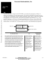
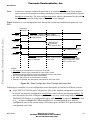
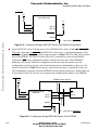
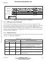
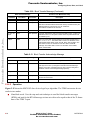
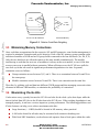
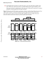
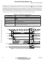
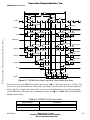
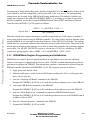
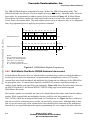
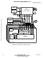
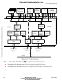
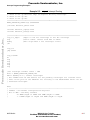
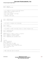
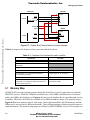
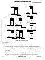
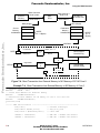
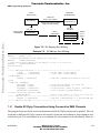
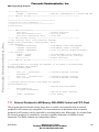
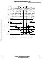
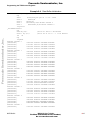
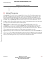
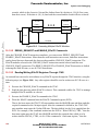
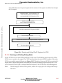
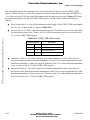
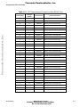
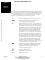
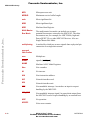
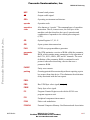
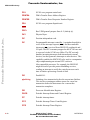
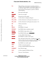
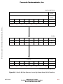
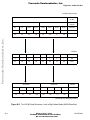
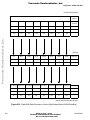
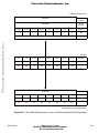
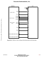
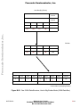
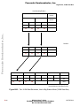
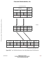
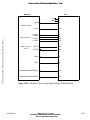
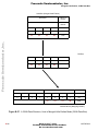
Figure 4-4. Flash Memory Write, Single-Master Bus Mode
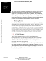
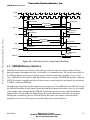
4.4 SDRAM Memory Interface
SDRAMs are the most cost effective, high capacity read/write memories on the market, offering
high-performance throughput with the cost benefits of a commodity item. The synchronous nature of
the SDRAM allows precise access timing control, with data transactions possible on every clock
cycle. SDRAMs are thus ideal for high-bandwidth memory systems. The SDRAM machine within the
MSC8102 memory controller provides all the necessary control functions and signals for interfacing
to JEDEC-compliant SDRAMs.
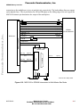
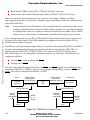
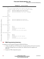
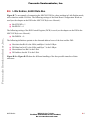
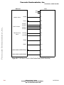
The following subsections detail the hardware connection of a 32-bit SDRAM to the MSC8102 using
the SDRAM controller in both Single-Master Bus and Multi-Master Bus modes. Next is a description
of the timing control settings and the SDRAM initialization procedure. Notice that the hardware
timings differ for both modes. In Single-Master Bus mode, the memory controller uses memory
timings and is completely glueless. In Multi-Master Bus mode, the memory controller allows
pipelined 60x accesses and requires an external address latch and multiplexor.
MOTOROLA
MSC8102 User’s Guide
For More Information On This Product,
Go to: www.freescale.com
4-7