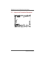
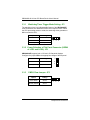
1
SBC84600VE 3.5” HDD Form Factor All-in-One CPU Board User’s Manual Disclaimers The information in this manual has been carefully checked and is believed to be accurate. AXIOMTEK Co., Ltd. assumes no responsibility for any infringements of patents or other rights of third parties which may result from its use. AXIOMTEK assumes no responsibility for any inaccuracies that may be contained in this document. AXIOMTEK makes no commitment to update or to keep current the information contained in this manual. AXIOMTEK reserves the right to make improvements to this document and/or product at any time and without notice. No part of this document may be reproduced, stored in a retrieval system, or transmitted, in any form or by any means, electronic, mechanical, photocopying, recording, or otherwise, without the prior written permission of AXIOMTEK Co., Ltd. Copyright 2003 by AXIOMTEK Co., Ltd. All rights reserved. July 2003, Version A2 Printed in Taiwan ii ESD Precautions Integrated circuits on computer boards are sensitive to static electricity. To avoid damaging chips from electrostatic discharge, observe the following precautions: Do not remove boards or integrated circuits from their anti-static packaging until you are ready to install them. Before handling a board or integrated circuit, touch an unpainted portion of the system unit chassis for a few seconds. This helps to discharge any static electricity on your body. Wear a wrist-grounding strap, available from most electronic component stores, when handling boards and components. Trademarks Acknowledgments AXIOMTEK is a trademark of AXIOMTEK Co., Ltd. IBM is a registered trademark of International Business Machines Corporation. MS-DOS, and Windows 98/NT/2000/XP are trademarks of Microsoft Corporation. Award is a trademark of Award Software, Inc. IBM, PC/AT, PS/2, VGA are trademarks of International Business Machines Corporation. VIA C3 and other trademarks of VIA Technology. Realtek RTL-8139C are registered trademark of Realtek Semiconductor Corporation. Other brand names and trademarks are the properties and registered brands of their respective owners. - iii This page does not contain any information. iv Table of Contents Chapter 1 Introduction -------------------------------------------1 1.1 General Description -------------------------------------------- 1 1.2 Specifications ---------------------------------------------------- 2 Chapter 2 Installation---------------------------------------------5 2.1 Installation Steps------------------------------------------------ 5 2.2 Peripherals for a Minimum System ----------------------- 5 Chapter 3 Jumpers and Connectors ---------------------------7 3.1 Jumpers and Connectors Layout-------------------------- 7 3.2 Jumpers and Connectors Dimensions------------------- 8 3.3 Jumper Settings ------------------------------------------------- 9 3.3.1 Watchdog Timer Trigger Mode Setting: JP1 ------------------ 10 3.3.2 Power Selection of Flat Panel Connector (VDDM of LCD1 and LCD2): JP2 ------------------------------------------------------------ 10 3.3.3 CMOS Clear Jumper: JP3 ----------------------------------------- 10 3.3.4 COM2 RS232/422/485 Settings: JP4, JP5, JP6 ---------------- 11 3.3.5 Power Supply Type Selection: JP7------------------------------- 11 3.3.6 COM2 Signal/+5V Selection: JP8 ------------------------------- 11 3.3.7 COM1 Signal/+5V Selection: JP9 ------------------------------- 11 3.3.8 COM4 Signal/+5V Selection: JP10------------------------------ 12 3.3.9 COM3 Signal/+5V Selection: JP11 ------------------------------ 12 3.3.10 Compact Flash Voltage Selection: JP12 ----------------------- 12 3.4 Connectors ------------------------------------------------------ 13 3.4.1 Enhanced IDE Interface Connector: CN1 --------------------- 14 3.4.2 Flat Panel Bezel Connector: CN3 ------------------------------- 15 3.4.3 VGA/Flat Panel Connector: VGA1, CN2, CN4 --------------- 16 3.4.4 CPU Fan Connector: CN5 ---------------------------------------- 22 3.4.5 Parallel Port: CN7 -------------------------------------------------- 23 3.4.6 Digital I/O Port (DIO1): CN8 ----------------------------------- 24 3.4.7 ATX Power On /Off Button: CN9 ------------------------------ 25 3.4.8 Power Input Connector: CN10 ---------------------------------- 25 3.4.9 IrDA Connector: CN11 -------------------------------------------- 26 3.4.10 AC97 Interface Link Connector: CN12 ------------------------ 26 3.4.11 Keyboard and PS/2 Mouse Connectors: CN13 -------------- 27 Table of Contents v 3.4.12 Composite Video Output: CN14, VIDEO1 (Optional Feature) ------------------------------------------------------------ 27 3.4.13 FDD Connector: CN15 ------------------------------------------- 28 3.4.14 Mini Pci Type I Connector: CN16 ----------------------------- 28 3.4.15 USB Connectors: USB1 and USB2 ----------------------------- 29 3.4.16 Ethernet PJ-45 Connector: LAN1 ------------------------------ 30 3.4.17 PC/104 Connectors: J1 and J2----------------------------------- 31 3.4.18 Serial Port Interface ----------------------------------------------- 32 3.4.19 Compact Flash Connector: CF1 -------------------------------- 33 Chapter 4 Hardware Description ---------------------------- 35 4.1 4.2 4.3 4.4 4.5 4.6 4.7 Microprocessors ---------------------------------------------- 35 BIOS ------------------------------------------------------------- 35 Real Time Clock and CMOS RAM------------------------ 35 System Memory------------------------------------------------ 35 VGA Interface--------------------------------------------------- 36 I/O Port Address Map ---------------------------------------- 37 Interrupt Controller ------------------------------------------- 38 Chapter 5 Award BIOS Utility ------------------------------- 39 5.1 BIOS Introduction --------------------------------------------- 39 5.2 BIOS Setup ------------------------------------------------------ 39 5.2.1 Standard CMOS Setup--------------------------------------------- 41 5.2.2 Advanced BIOS Features ----------------------------------------- 45 5.2.3 Advanced Chipset Features -------------------------------------- 50 5.2.4 Integrated Peripherals --------------------------------------------- 53 5.2.5 Power Management Setup ---------------------------------------- 56 5.2.6 PNP/PCI Configuration ------------------------------------------ 59 5.2.7 PC Health Status --------------------------------------------------- 61 5.2.8 Frequency/Voltage Control -------------------------------------- 62 5.2.9 Load Fail-Safe Defaults ------------------------------------------- 63 5.2.10 Load Optimized Defaults---------------------------------------- 64 5.2.11 Set Supervisor/User Password ---------------------------------- 65 5.2.12 Save & Exit Setup ------------------------------------------------- 66 5.2.13 Exit Without Saving ---------------------------------------------- 67 Appendix A Watchdog Timer -------------------------------- 69 vi Table of Contents SBC84600 All-in-One CPU Board Series User’s Manual Chapter 1 Introduction 1.1 General Description The SBC84600VE is a featured-pack CPU Board designed for industrial purpose. It provides reliable high performance and functionrich capability. The onboard CPU incorporates the VIA VT8606 chipset and the VT82C686B with built-in AGP-4x VGA controller; the PC/104 bus is available for further expansions. Its 8-layer structure reduces signal noise and meets ACPI function with its built-in power management feature. Designed for the professional embedded developers, this SBC84600VE is virtually an ultimate one-step solution to various applications. It provides fanless possibility for critical application environmemts with low power consumption design to improve system MTBF. Introduction 1 SBC84600 All-in-One CPU Board Series User’s Manual 1.2 Specifications Processor: VIA EDEN 400MHz, 667MHZ,or C3 800MHz (C3 1GHz CPU or other frequency processors are manufacturer optional) L2 Cache: Integrated in CPU Chipset: VT8606 (Twister-T) + VT82C686B System Memory: One 144-pin DIMM socket Maximum up to 512MB SDRAM BIOS: AWARD BIOS, Plug-and-Play 4Mbit Flash ROM with SmartView VGA BIOS Function and integrated Ethernet Novell RPL and Windows PXE Boot ROM functions Watchdog Timer: Generates a system reset or NMI by jumper selectable Software programmable time interval 64 levels, 0.5~8/5~80/50~800/100~1600 seconds Standard I/O: Four serial ports, including three RS-232 and one RS-232/422/485 One parallel port, SPP/EPP/ECP One HDD Interface One FDD Interface One PS/2 Keyboard & Mouse Interface One IrDA interface for wireless communication USB Interface: 2 USB ports with USB Spec. Rev. 1.1a compliant Ethernet: Realtek 8139C PCI Bus 10/100M Base-T Wake On LAN (via ATX power supply) Onboard RJ-45 connector Digital I/O: 8-channel TTL/DTL compatible input and output Board ID: Dallas DS2401 Board unique ID support Solid State Disk Interface: 2 Introduction SBC84600 All-in-One CPU Board Series User’s Manual One CompactFlash Type II Socket Expansion Slot: one 16-bit pc/104 connector AC97 Link: AC97 Link intelface for external audio Cedoec Kit (AX93100) Drivers: VIA Chipset Driver Ethernet Utility and Drivers VGA Drivers Introduction 3 SBC84600 All-in-One CPU Board Series User’s Manual This page does not contain any information. 4 Introduction SBC84600 All-in-One CPU Board Series User’s Manual Chapter 2 Installation 2.1 Installation Steps Follow the steps listed below to install the SBC84600VE in the system. 1. Make sure the power is OFF. 2. Set the configuration jumpers according to the jumper settings in Chapter 3. 3. Connect the I/O cables and peripherals, i.e. floppy disk, hard disk, monitor, keyboard, power supply and etc. to the CPU board. NOTE: 2.2 The color of pin one is usually red or blue, while others are gray. Peripherals for a Minimum System The followings is a list of typical peripherals required to build a minmum system: AT or ATX Power supply IBMTM PS/2 keyboard And Mouse Display monitor Floppy or hard disk with MS-DOS or Flash Disk emulator Installation 5 SBC84600 All-in-One CPU Board Series User’s Manual This page does not contain any information. 6 Installation SBC84600 All-in-One CPU Board Series User’s Manual Chapter 3 Jumpers and Connectors 3.1 Jumpers and Connectors Layout JP1 CN1 CN3 CN2 CN7 CN9 CN4 JP2 CN8 CN5 JP3 JP4 COM1 Jumpers and Connectors CN10 CN1 COM3 COM2 CN11 JP11 JP10 JP8 JP9 JP5 JP6 COM4 J2 J1 JP12 VIDEO1 CN12 USB1 USB2 CN14 CN13 LAN1 JP7 VGA1 7 SBC84600 All-in-One CPU Board Series User’s Manual 143.05 146.05 117.60 104.65 100.86 98.37 98.04 96.34 93.60 68.91 17.27 47.17 Jumpers and Connectors Dimensions 1.30 3.2 100.84 98.37 94.26 87.25 101.75 91.06 17.40 12.95 11.94 9.78 8 6.83 7.62 5.51 3.18 143.05 111.51 91.92 77.27 63.27 45.34 40.46 28.78 15.16 18.62 4.83 6.60 8.89 0.00 1.52 4.83 3.18 0.00 23.47 140.97 15.57 113.54 65.53 87.25 73.28 Jumpers and Connectors SBC84600 All-in-One CPU Board Series User’s Manual 3.3 Jumper Settings Making the proper jumper settings configure the SBC84600VE to match the needs of your application. The following table shows the default jumper settings for the onboard devices. Jumper Default Setting Jumper Setting JP1 Watchdog Trigger Mode: Disabled JP2 Flat Panel Power Selection: VDDM at 3.3V Short 2-3 JP3 Clear CMOS Setting: Normal Short 1-2 JP4 COM2 Port Setting: RS-232 Short 1-2 JP5 COM2 Port Setting: RS-232 Short 3-5, 4-6 JP6 COM2 Port Setting: RS-232 Short 3-5, 4-6 JP7 Power Supply Selection: AT power supply Short 1-2 JP8 COM2 Signal/+5V Selection Default: COM Signal Short 2-3 JP9 COM1 Signal/+5V Selection Default: COM Signal Short 2-3 JP10 COM4 Signal/+5V Selection Default: COM Signal Short 2-3 JP11 COM3 Signal/+5V Selection Default: COM Signal Short 2-3 JP12 Compact Flash Voltage Selection Default: 3.3V Short 1-2 Jumpers and Connectors Open 9 SBC84600 All-in-One CPU Board Series User’s Manual 3.3.1 Watchdog Timer Trigger Mode Setting: JP1 The watchdog timer is an indispensable feature of the SBC84600VE. It has a sensitive error detection function and a report function. When the CPU processing comes to a halt, the watchdog either generates a NMI or resets the CPU. Options Setting NMI Short 1-2 RESET Short 2-3 Disabled (default) Open 1 2 3 3.3.2 Power Selection of Flat Panel Connector (VDDM of LCD1 and LCD2): JP2 SBC84600VE supports both +3.3V and +5V flat panel displays. Configure the jumper JP2 to the appropriate voltage of the flat panel VDDM Settings 1 5V Short 1-2 2 3.3V (default) Short 2-3 3 . 3.3.3 10 CMOS Clear Jumper: JP3 Options Settings Clear CMOS Short 2-3 Normal (default) Short 1-2 1 2 3 Jumpers and Connectors SBC84600 All-in-One CPU Board Series User’s Manual 3.3.4 COM2 RS232/422/485 Settings: JP4, JP5, JP6 COM2 JP4 RS-232 (default) Short 1-2 RS-422 Short 3-4 RS-485 Short 5-6, 7-8 JP5 JP6 Short 3-5, 4-6 Short 1-3, 2-4 Short 1-3, 2-4 Short 3-5, 4-6 Short 1-3, 2-4 Short 1-3, 2-4 JP5 and JP6 JP4 3.3.5 3.3.6 8 7 6 5 4 3 2 1 5 3 1 6 4 2 Power Supply Type Selection: JP7 Options Settings 3 AT P/S Short 1-2(default) 2 ATX P/S Short 2-3 1 COM2 Signal/+5V Selection: JP8 Options Setting JP8 3 3.3.7 Pin 1=+5V Short 1-3 Pin 1=DCD Short 2-3 (default) 2 1 COM1 Signal/+5V Selection: JP9 JP9 Options Setting Pin 1=+5V Short 1-3 2 Pin 1=DCD Short 2-3(default) 1 Jumpers and Connectors 3 11 SBC84600 All-in-One CPU Board Series User’s Manual 3.3.8 COM4 Signal/+5V Selection: JP10 Options Setting Pin 1=+5V Short 1-3 Pin 1=DCD Short 2-3 (default) JP10 3 3.3.9 2 1 COM3 Signal/+5V Selection: JP11 Options Setting Pin 1=+5V Short 1-3 Pin 1=DCD Short 2-3 (default) JP11 3 2 1 3.3.10 Compact Flash Voltage Selection: JP12 Options Setting 5V Short 2-3 3.3V Short 1-2(default) JP12 3 12 2 1 Jumpers and Connectors SBC84600 All-in-One CPU Board Series User’s Manual 3.4 Connectors The connectors allow the CPU Board to connect with other parts of the system. Ensure that all connectors are in place and firmly attached. The following table lists the function of each connector on the SBC84600VE. Connectors 44 Pin IDE Connector 44-pin LCD Connector Flat Panel Bezel Connector 20-pin LCD Connector CPU FAN +5V Connector Printer Port Connector Digital I/O Port Conntctor ATX Power On/Off Button Power Input Connectors IrDA Connector AC97 Link Interface Keyboard and Mouse Conntctor TV Connector FDD Connector Mini pci Type I USB connector VGA CRT Connector Ethernet Connector PC/104 Connector COM Connector COM Connector COM Connector COM Connector Compact Flash Connector VIDEO Connector Jumpers and Connectors Label CN1 CN2 CN3 CN4 CN5 CN7 CN8 CN9 CN10 CN11 CN12 CN13 CN14 CN15 CN16 USB1, USB2 VGA1 LAN1 J1, J2 COM1 COM2 COM3 COM4 CF1 VIDEO1 13 SBC84600 All-in-One CPU Board Series User’s Manual 3.4.1 Enhanced IDE Interface Connector: CN1 The SBC84600VE includes a PCI bus enhanced IDE controller that can support master/slave mode and post write transaction mechanisms with 64-byte buffer and master data transaction. 44-pin IDE Interface Connector: Pin 14 Description Pin Description Pin Description 1 Reset # 2 GND 3 Data 7 4 Data 8 5 Data 6 6 Data 9 7 Data 5 8 Data 10 9 Data 4 10 Data 11 11 Data 3 12 Data 12 13 Data 2 14 Data 13 15 Data 1 16 Data 14 17 Data 0 18 Data 15 19 GND 20 No connector 21 No connector 22 GND 23 IOW # 24 GND 25 IOR # 26 GND 27 IOCHRDY 28 No connector 29 No connector 30 GND-Default 31 Interrupt 32 No connector 33 SA1 34 No connector 35 SA0 36 SA2 37 HDC CS0 # 38 HDC CSI # 39 HDD Active # 40 GND 41 VCC 42 VCC 43 GND 44 N.C Jumpers and Connectors SBC84600 All-in-One CPU Board Series User’s Manual 3.4.2 Flat Panel Bezel Connector: CN3 CN3 Power LED This 2-pin connector, designated at Pins 1 and 5, connects the system power LED indicator to its respective switch on the case. Pin 1 is +, and pin 5 is assigned as -. The Power LED lights up when the system is powered ON. External Speaker and Internal Buzzer Connector Pins 2, 4, 6, and 8 of CN3 connect to the case-mounted speaker unit or internal buzzer. Short pins 4-6 when connecting the CPU card to an internal buzzer. When connecting an external speaker, set these jumpers to Open and install the speaker cable on pin 8 (+) and pin 2 (-). System Reset Switch Pins 9 & 11 of CN3 connect to the case-mounted reset switch and allow rebooting of your computer instead of turning OFF the power switch. This is a preferred method of rebooting in order to prolong the life of the system’s power supply. HDD Activity LED This connector extends to the hard drive activity LED on the control panel. This LED will flash when the HDD is being accessed. Pins 10 & 12 of CN3 connect the hard disk drive and the front panel HDD LED. Pins 10 is -, and pin 12 is assigned as +. Jumpers and Connectors 15 SBC84600 All-in-One CPU Board Series User’s Manual 3.4.3 VGA/Flat Panel Connector: VGA1, CN2, CN4 The SBC84600VE has three connectors that support CRT VGA and flat panel displays, individually or simultaneously. VGA1 is a standard 15-pin pin header connector commonly used for the CRT VGA display, and CN2 (44-pin) CN4 (20-pin) are dual-in-line headers for the flat panel connection. Configuration of the VGA interface is done via the software utility and no jumper setting is required. The following two tables are the pin assignments for the CRT/VGA connector and the flat panel connector. VGA1: CRT/VGA Connector Pin Assignment Pin Description Pin Description Pin Description 1 Red 2 Green 3 Blue 4 N/A 5 GND 6 AGND 7 AGND 8 AGND 9 N/A 10 GND 11 N/A 12 DDC DAT 13 Horizontal Sync 14 Vertical Sync 15 DDC CLK Description CN2: Flat Panel Connector Pin Assignment Pin Description Pin Description Pin 1 -12V 2 +12VM 3 GND 4 GND 5 VDDM 6 VDDM 7 ENAVEE 8 GND 9 P0 10 P1 11 P2 12 P3 13 P4 14 P5 15 P6 16 P7 17 P8 18 P9 19 P10 20 P11 21 P12 22 P13 23 P14 24 P15 25 P16 26 P17 27 P18 28 P19 29 P20 30 P21 31 P22 32 P23 33 GND 34 GND 35 SHFCLK 36 FLM 37 M 38 LP 39 GND 40 ENABKL 41 GND 42 -SHFCLK 43 VDDM 44 VDDM 16 Jumpers and Connectors SBC84600 All-in-One CPU Board Series User’s Manual CN4: Flat Panel Connector for XVGA Pin Description Pin Description Pin Description 1 GND 2 GND 3 P24 4 P25 5 P26 6 P27 7 P28 8 P29 9 GND 10 GND 11 P30 12 P31 13 P32 14 P33 15 P34 16 P35 17 VDDM 18 VDDM 19 +12VM 20 +12VM 3.4.3.1 Flat Panel Connector Pin Description Name Description P0~P35 Flat panel data output ENABKL Activity Indicator and Enable Backlight outputs SHFCLK Shift clock. Pixel clock for flat panel data M M signal for panel AC drive control LP Latch pulse. Flat panel equivalent of HSYNC FLM +12VM ENAVEE / ENAVDD VDDM First line marker. Flat panel equivalent of VSYNC +12V power controlled by chipset Power sequencing controls for panel LCD bias volt 3.3V or 5V power controlled by chipset and selected by JP6 Jumpers and Connectors 17 SBC84600 All-in-One CPU Board Series User’s Manual 3.4.3.2 Flat Panel Interface Pins for Color DSTN and Color TFT LCD (Twister-T VT8606) Pin LP FLM SHFCLK M ENAVDD ENABLK P0 P1 P2 P3 P4 P5 P6 P7 P8 P9 P10 P11 P12 P13 P14 P15 P!6 P17 P18 P19 P20 P21 P22 P23 P24 18 STN DSTN 8-bit 16-bit 24-bit 8-bit LP FP XCK DE ENAVDD ENABLK R0 G0 B0 R1 G1 B1 R2 G2 LP FP XCK DE ENAVDD ENABLK R0 G0 B0 R1 G1 B1 R2 G2 B2 R3 G3 B3 R4 G4 B4 R5 HSYNC VSYNC CK DE ENAVDD ENABLK R0 G0 B0 R1 G1 B1 R2 G2 B2 R3 G3 B3 R4 G4 B4 R5 G5 B5 R6 G6 B6 R7 G7 B7 HSYNC VSYNC CK DE ENAVDD ENABLK LR0 LG0 LB0 LR1 UR0 UG0 UB0 UR1 Jumpers and Connectors SBC84600 All-in-One CPU Board Series User’s Manual Pin LP FLM SHFCLK M ENAVDD ENABLK DSTN 16-bit LP FP XCK DE ENAVDD ENABLK P0 P1 P2 P3 LB1 LB0 P4 P5 P6 P7 UB1 UB0 P8 P9 P10 P11 LG1 LG0 P12 P13 P14 P15 UG1 UG0 P!6 P17 P18 P19 LR1 LR0 P20 P21 P22 P23 UR1 UR0 P30 TFT 24-bit LP FP XCK DE ENAVDD ENABLK LB3 LB2 LB1 LB0 UB3 UB2 UB1 UB0 LG3 LG2 LG1 LG0 UG3 UG2 UG1 UG0 LR3 LR2 LR1 LR0 UR3 UR2 UR1 UR0 9-bit HSYNC VSYNC CK DE ENAVDD ENABLK 2X9-bit HSYNC VSYNC CK DE ENAVDD ENABLK R0 R00 R10 R01 R11 R02 R12 R1 R2 G0 G1 G2 B0 P31 P32 B1 P33 P34 P35 Jumpers and Connectors B2 G00 G10 G01 G11 G02 G12 B00 B10 B01 B11 B02 B12 19 SBC84600 All-in-One CPU Board Series User’s Manual Pin LP FLM SHFCLK M ENAVDD ENABLK TFT TFT 12-bit 2X12-bit 15-bit 2X15-bit LP FP XCK DE ENAVDD ENABLK LP FP XCK DE ENAVDD ENABLK HSYNC VSYNC CK DE ENAVDD ENABLK HSYNC VSYNC CK DE ENAVDD ENABLK R0 R00 R10 R01 R11 R02 R12 R03 R13 R04 R14 P0 P1 P2 P3 P4 R0 P5 P6 R1 P7 P8 R2 P9 P10 R3 P11 R00 R10 R01 R11 R02 R12 R03 R13 R1 R2 R3 R4 P12 P13 G0 P14 P15 P!6 G0 P17 P18 G1 P19 P20 G2 P21 P22 P23 G3 G00 G10 G01 G11 G02 G12 G03 G13 G1 G2 G3 G4 G00 G10 G01 G11 G02 G12 G03 G13 G04 G14 P24 P25 P26 P27 20 B0 B00 B10 Jumpers and Connectors SBC84600 All-in-One CPU Board Series User’s Manual Pin P28 TFT 2X12-bit 15-bit 2X15-bit B0 B00 B10 B01 B11 B02 B12 B03 B13 B1 B01 B11 B02 B12 B03 B13 B04 B14 P29 P30 B1 P31 P32 B2 P33 P34 B3 P35 Pin LP FLM SHFCLK M ENAVDD ENABLK P1 P3 P4 P5 P6 P7 B0 B1 B2 B3 B4 B5 P8 P9 P10 P11 P12 P13 P14 P15 G0 G1 G2 G3 G4 G5 P16 P17 P18 B2 B3 B4 TFT 18-bit LP FP XCK DE ENAVDD ENABLK P0 P2 TFT 12-bit R0 Jumpers and Connectors TFT 24-bit LP FP XCK DE ENAVDD ENABLK B0 B1 B2 B3 B4 B5 B6 B7 G0 G1 G2 G3 G4 G5 G6 G7 R0 R1 R2 2X18-bit HSYNC VSYNC CK DE ENAVDD ENABLK R00 R10 R01 R11 R02 R12 R03 R13 R04 R14 R05 R15 G00 G10 G01 G11 G02 G12 G03 21 SBC84600 All-in-One CPU Board Series User’s Manual Pin P19 P20 P21 P22 P23 TFT 18-bit R1 R2 R3 R4 R5 TFT 24-bit R3 R4 R5 R6 R7 P24 P25 P26 P27 P28 P29 P30 P31 P32 P33 P34 P35 3.4.4 22 2X18-bit G13 G04 G14 G05 G15 B00 B10 B01 B11 B02 B12 B03 B13 B04 B14 B05 B15 CPU Fan Connector: CN5 Pin Description 1 GND 2 +5V Jumpers and Connectors SBC84600 All-in-One CPU Board Series User’s Manual 3.4.5 Parallel Port: CN7 The SBC84600VE has a multi-mode parallel port, CN7, to support: Standard mode: IBM PC/XT, PC/AT and PS/2 compatible with bi-directional parallel port Enhanced mode: Enhance parallel port (EPP) compatible with EPP 1.7 and EPP 1.9 (IEEE 1284 compliant) High speed mode: Microsoft and Hewlett Packard extended capabilities port (ECP) IEEE 1284 compliant The address select of the onboard parallel port in LPT1 (3BCH) or disabled is done by BIOS CMOS setup. Pin Description Pin Description 1 Strobe# 14 Auto Form Feed# 1 2 2 Data 0 15 Error# 3 4 3 Data 1 16 Initialize# 5 6 7 9 8 10 11 12 13 15 14 16 4 Data 2 17 Printer Select In# 5 Data 3 18 GND 6 Data 4 19 GND 7 Data 5 20 GND 8 Data 6 21 GND 9 Data 7 22 GND 17 19 18 20 10 Acknowledge# 23 GND 21 22 11 Busy 24 GND 12 Paper Empty# 25 GND 23 25 24 26 13 Printer Select 26 NC Jumpers and Connectors 23 SBC84600 All-in-One CPU Board Series User’s Manual 3.4.6 Digital I/O Port (DIO1): CN8 The board is equipped with an 8-channel digital I/O connector CN8 that meets a system customary automation control needs. The digital I/O can be configured to control the cash drawer, or to sense the warning signal of an Uninterrupted Power System (UPS), or to perform the store security control. The digital I/O is controlled via software programming. Digital I/O Connector: CN8 Pin 1 3 5 7 9 11 13 15 17 19 3.4.6.1 Signal DIO Out 0 DIO Out 1 DIO Out 2 DIO Out 3 DIO Out 4 DIO Out 5 DIO Out 6 DIO Out 7 GND NC Pin 2 4 6 8 10 12 14 16 18 20 Signal DIO In 0 DIO In 1 DIO In 2 DIO In 3 DIO In 4 DIO In 5 DIO In 6 DIO In 7 GND NC 20 2 1 Digital I/O Software Programming The Digital I/O on the board is not an isolated type. Output Address Bit Output Address Out-0 123h 0 In-0 123h Out-1 123h 1 In-1 123h Out-2 123h 2 In-2 123h Out-3 123h 3 In-3 123h Out-4 123h 4 In-4 123h Out-5 123h 5 In-5 123h Out-6 123h 6 In-6 123h Out-7 123h 7 In-7 123h Example program; Out 123h, 03h Out-0, Out-1 Out-2, Out-3 Out 123h, 0Ah Out-0, Out-2 Out-1, Out-3 Turn On 24 19 Bit 0 1 2 3 4 5 6 7 Turn On Turn Off Turn Off Jumpers and Connectors SBC84600 All-in-One CPU Board Series User’s Manual Example program; If INPUT 123 is (1011), then INPUT-2 is “0” If INPUT 123 is (1100), then INPUT-0 & 1 are “0” ** The INPUT signal has to be TTL signal 3.4.7 ATX Power On /Off Button: CN9 This 2-pin connector, CN9, connects the ATX power button of the front panel to the Board allowing user to control the power on/off state of the ATX power supply. This jumper is only useful when installing an ATX power supply. 3.4.8 Pin Signal Name 1 PW_BN+ 2 GND Power Input Connector: CN10 Pin Description 1 +5V 2 GND 3 +12V 4 SB5V 5 PS_ON 6 -12V 7 GND 8 +5V Jumpers and Connectors CN10 25 SBC84600 All-in-One CPU Board Series User’s Manual 3.4.9 IrDA Connector: CN11 CN11 is a 5-pin IrDA connector for wireless communication. CN11 +5V 1 N.C. 2 IRRX 3 GND 4 IRTX 5 3.4.10 AC97 Interface Link Connector: CN12 CN12 is a AC97 Interface Link Connector for Audio KIT. CN12 26 Jumpers and Connectors SBC84600 All-in-One CPU Board Series User’s Manual 3.4.11 Keyboard and PS/2 Mouse Connectors: CN13 The SBC84600VE provides a keyboard and Mouse interface. CN13 is a DIN connector for PS/2 keyboard Connection VIA “Y” Cable CN13 Keyboard Clock Mouse Clock 6 5 4 VCC Mouse Data 3 2 1 GND Keyboard Data 3.4.12 Composite Video Output: CN14, VIDEO1 (Optional Feature) The SBC84600VE provides a PC99 compliant soulution for TV output. Composite Video Output: CN14 Pin Signal 1. COMP/Y/G GND 2 S-Video Output: VIDEO1 Pin Signal GND CSYNC CHROMA/V/R LUMA/U/B The S-Video Output is use a 4 pin Wafer with box 2.0mm 1 2 3 4 Jumpers and Connectors 27 SBC84600 All-in-One CPU Board Series User’s Manual 3.4.13 FDD Connector: CN15 The SBC84600VE provides a 26-pin FCC Z.I.F. type connector, and the general output supports a single floppy drives. The floppy drive could be any one of the following types: 3.5" 720KB or 1.44MB/2.88MB. CN15: FDD Connector Pin Assignment Pin Description Pin Description 1 2 3 4 5 6 7 8 9 10 11 12 13 +5V INDEX +5V DRIVE0 +5V DSKCHG No connector READY HDOUT MOTOR ON No connector DIR HDSEL 14 15 16 17 18 19 20 21 22 23 24 25 26 STEP GND WDATA GND WGATE GND TRK0 GND WPT GND RDATA GND SIDE0 3.4.14 Mini Pci Type I Connector: CN16 CN16: Connector Pin Assignment Pin Description Pin Description Pin 1 INTB 2 +5V 3 +3V 4 INTA 5 RESERVED 6 RESERVED 28 Description 7 GND 8 N.C 9 CLK 10 PCIRST- 11 GND 12 +3V 13 REQ0- 14 GNT0- 15 +3V 16 GND 17 AD31 18 PME- 19 AD29 20 N.C 21 GND 22 AD30 23 AD27 24 +3V 25 AD25 26 AD28 27 RESERVED 28 AD26 29 CBE-3 30 AD24 31 AD23 32 IDSEL (AD28) 33 GND 34 GND 35 AD21 36 AD22 Jumpers and Connectors SBC84600 All-in-One CPU Board Series User’s Manual Pin Description Pin Description Pin 37 AD19 38 AD20 39 Description GND 40 PAR 41 AD17 42 AD18 43 CBE-2 44 GND 45 IRDY- 46 GND 47 +3V 48 FRAME- 49 N.C 50 TRDY- 51 SERR- 52 STOP- 53 GND 54 +3V 55 PERR- 56 DEVSEL- 57 CBE-1 58 GND 59 AD14 60 AD15 61 GND 62 AD13 63 AD12 64 AD11 65 AD10 66 GND 67 GND 68 AD9 69 AD8 70 CBE-0 71 AD7 72 +3V 73 +3V 74 AD6 75 AD5 76 AD4 77 RESERVED 78 AD2 79 AD3 80 AD0 81 +5V 82 RESERVED 83 AD1 84 N.C 85 GND 86 GND 87 N.C 88 N.C 89 N.C 90 N.C 91 N.C 92 N.C 93 N.C 94 N.C 95 N.C 96 N.C 97 N.C 98 GND 99 N.C 100 N.C 3.4.15 USB Connectors: USB1 and USB2 There are two USB connectors allow installation of USB devices. USB1 is 4-pin header connector, and USB2 is a single standard USB connector. The following table shows the pin outs of the USB connectors. Pin # Signal Name 1 USB Vcc 2 USB - 3 USB + 4 USB GND Jumpers and Connectors 29 SBC84600 All-in-One CPU Board Series User’s Manual 3.4.16 Ethernet PJ-45 Connector: LAN1 The SBC84600VE is equipped with a high performance Plug and Play Ethernet interface which is fully compliant with the IEEE 802.3 standar, and consisting of a RJ-45 connector LAN . 3.4.16.1 Pin Assignment LAN1: RJ-45 Connector Pin Assignment Pin 1 2 3 4 5 6 7 8 Signal Tx+ (Data transmission positive Tx- (Data transmission negative) Rx+(Data reception positive) RJ45 termination RJ45 termination Rx- (Data reception negative) RJ45 termination RJ45 termination 1 2 3 4 5 6 7 8 RJ-45 3.4.16.2 Feature 10Mb/s and 100Mb/s operations Supports 10Mb/s and 100Mb/s N-Way auto negotiation Full duplex capability Full compliance with PCI Revision 2.1 PCI Bus Master data transfers 3.4.16.3 Drivers Supported Bundled with popular software drivers, the SBC84600VE Ethernet interface allows great flexibility to work with all major networking operating systems including Novell NetWare v2.x, v3.x, v4.x, Microsoft LAN Manager, Win3.1, Win NT, Win95, IBM LAN Server, SCO UNIX or other ODI, NDIS and Packet drive compliant operating systems. 30 Jumpers and Connectors SBC84600 All-in-One CPU Board Series User’s Manual 3.4.17 PC/104 Connectors: J1 and J2 The PC/104 is an industrial standard. It is a compact form factor with dimensions of 3.6” x 3.8” and is fully compatible with the ISA Bus. The PC/104 interface is able to adapt the off-the-shelf PC/104 modules, such as sound module, fax modem module, multi-I/O module, and etc. J1: PC/104 Bus Pin Assignment Pin# 1 5 9 13 17 21 25 29 33 37 41 45 49 53 57 61 Pin Name IOCHCHK SD6 SD4 SD2 SD0 AEN SA18 SA16 SA14 SA12 SA10 SA8 SA6 SA4 SA2 SA0 Pin# 2 6 10 14 18 22 26 30 34 38 42 46 50 54 58 62 Pin Name GND +5V -5V -12V +12V SMEMW IOW DACK3 DACK1 REFRESH IRQ7 IRQ5 IRQ3 TC +5V GND Pin# 3 7 11 15 19 23 27 31 35 39 43 47 51 55 59 63 Pin Name SD7 SD5 SD3 SD1 IOCHRDY SA19 SA17 SA15 SA13 SA11 SA9 SA7 SA5 SA3 SA1 GND Pin# Pin Name 4 RESETDRV IRQ9 DRQ2 ENDXFR GND SMEMR IOR DRQ3 DRQ1 SYSCLK IRQ6 IRQ4 DACK2 SALE OSC GND 8 12 16 20 24 28 32 36 40 44 48 52 56 60 64 J2: PC/104 Bus Pin Assignments Pin# 1 5 9 13 17 21 25 29 33 37 Pin Name GND IOCS16 IRQ11 IRQ15 DACK0 DACK5 DACK6 DACK7 +5V GND Pin# 2 6 10 14 18 22 26 30 34 38 Pin Name GND LA23 LA21 LA19 LA17 MEMW SD9 SD11 SD13 SD15 Jumpers and Connectors Pin# 3 7 11 15 19 23 27 31 35 39 Pin Name MEMCS16 IRQ10 IRQ12 IRQ14 DRQ0 DRQ5 DRQ6 DRQ7 MASTER GND Pin# 4 8 12 16 20 24 28 32 36 40 Pin Name SBHE LA22 LA20 LA18 MEMR SD8 SD10 SD12 SD14 (KEY) 31 SBC84600 All-in-One CPU Board Series User’s Manual 3.4.18 Serial Port Interface 3.4.18.1 COM Port Connector: COM1 The connector, COM 1, is a DB-9 connector, and the following table shows the pin assignments of this connector. Pin 1 2 3 4 5 6 7 8 9 Signal Name DCD, Data carrier detect RXD, Receive data TXD, Transmit data DTR, Data terminal ready GND, ground DSR, Data set ready RTS, Request to send CTS, Clear to send RI, Ring indicator COM1 3.4.18.2 COM Port Connectors: COM2, COM3, COM4 The RS-232 pin assignments are listed on the following table. Pin 32 Description Pin Description 1 Data Carrier Detect (DCD) 2 Data Set Ready (DSR) 3 Receive Data (RXD) 4 Request to Send (RTS) 5 Transmit Data (TXD) 6 Clear to Send (CTS) 7 Data Terminal Ready (DTR) 8 Ring Indicator (RI) 9 Ground (GND) 10 NC 1 2 3 4 5 6 7 9 8 10 Jumpers and Connectors SBC84600 All-in-One CPU Board Series User’s Manual The RS-422/485 pin assignments for COM2 are listed below. Pin # 1 2 3 4 5 6 7 8 9 10 Signal Name R2-422 RS-485 TXNo connector TX+ No connector RX+ No connector RXNo connector GND No connector DATANo connector DATA+ No connector No connector No connector No connector No connector GND No connector 3.4.19 Compact Flash Connector: CF1 The SBC84600VE Series is equipped with a CompactFlash disk socket on the solder side and it supports the IDE2 interface CompactFlash disk card. The socket itself is specially designed to prevent any incorrect installation of the CompactFlash disk card. When installing or removing the CompactFlash disk card, make sure the system power is off. The CompactFlash disk card is defaulted as the E: or F: disk drive in the PC system. Jumpers and Connectors 33 SBC84600 All-in-One CPU Board Series User’s Manual This page does not contain any information. 34 Jumpers and Connectors SBC84600 All-in-One CPU Board Series User’s Manual Chapter 4 Hardware Description This chapter gives a detailed explaination of the hardware features of the SBC84600VE CPU Board. 4.1 Microprocessors The SBC84600VE supports VIA EDEN 400MHz, 667MHz,or C3 800MHz, C3 1G CPU (other frequency processors are manufacturer optional). Systems based on these CPUs can be operated under Windows XP/NT/2000/98/Me and MS-DOS environments. The system performance depends on the installed CPU on the board. 4.2 BIOS The system BIOS used in SBC84600VE is Award Plug and Play BIOS. The SBC84600VE contains a single 4M-bit Flash EPROM. 4.3 Real Time Clock and CMOS RAM The SBC84600VE contains VT82C686B Integrated Real Time Clock (RTC) and 128 bytes of CMOS RAM. The CMOS RAM stores the system configuration information entered via the SETUP program. A battery, with power lasting 10 years, keeps the stored information on the RTC and CMOS RAM active when system power is turned off. 4.4 System Memory SBC84600VE has one onboard 144-pin SODIMM socket that supports 16MB, 32MB, 64MB, 128MB, 256MB, and up to 512MB SODIMM modules. Hardware Description 35 SBC84600 All-in-One CPU Board Series User’s Manual 4.5 VGA Interface The Twister-T integrates S3 Graphics ’128-bit ProSavage4 graphics accelerator into a single chip. TwisterT brings mainstream graphics performance to the Value PC with leading-edge 2D, 3D and DVD video acceleration into a cost effective package. Based on its capabilities, Twister-T is an ideal solution for the consumer, corporateration users and entry-level professionals. The industry ’s first integrated AGP 4X solution, TwisterT combines AGP 4X performance with Microsoft Direct-X texture compression and assive 2Kx2K textures to deliver unprecedented 3D. High-Performance 3D Accelerator 128-bit 2D Graphics Engine DVD Playback and Video onferencing LCD and Flat Panel Monitor Support High Screen Resolution CRT Support 36 Hardware Description SBC84600 All-in-One CPU Board Series User’s Manual 4.6 I/O Port Address Map The CPU card communicates via I/O ports. It has a total of 1KB port addresses that can be assigned to other devices via I/O expansion cards. Address Devices 000-01F DMA controller #1 020-03F Interrupt controller #1 040-05F Timer 060-06F Keyboard controller 070-07F Real time clock, NMI 080-09F DMA page register 0A0-0BF Interrupt controller #2 0F0 Clear math coprocessor busy signal 0C0-0DF DMA controller #2 0F1 Reset math coprocessor 0F8-0FF Math processor 120 Disable watchdog timer operation (read) 121 Enable watchdog timer operation (read) 122 Watchdog 1F0-1F8 Fixed disk controller 200-207 Game port 300-31F Prototype card 360-36F Reserved 378-37F Parallel port #1 3B0-3BF MDA video card (including LPT1) 3C0-3CF EGA card 3D0-3DF CGA card 3F0-3F7 Floppy disk controller 3F8-3FF Serial port #1 (COM1) 2F8-2FF Serial port #2 (COM2) 3E8-3EF Serial port #3 (COM3) 2E8-2EF Serial port #4 (COM4) Hardware Description 37 SBC84600 All-in-One CPU Board Series User’s Manual 4.7 Interrupt Controller The SBC84600VE is a fully PC compatible control board. It consists of 16 ISA interrupt request lines and 4 of the 16 can be either ISA or PCI. The mapping list of the 16 interrupt request lines is shown below; NMI 38 Parity check error IRQ0 System timer output IRQ1 Keyboard IRQ2 Interrupt rerouting from IRQ8 through IRQ15 IRQ3 Serial port #2 IRQ4 Serial port #1 IRQ5 Reserved IRQ6 Floppy disk controller IRQ7 Parallel port #1 IRQ8 Real time clock IRQ9 Reserved IRQ10 Serial port #2 IRQ11 Serial port #2 IRQ12 PS/2 Mouse IRQ13 Math coprocessor IRQ14 Primary IDE channel IRQ15 Secondary IDE Channel Hardware Description SBC84600 All-in-One CPU Board Series User’s Manual Chapter 5 Award BIOS Utility Chapter 5 describes the different settings available in the Award BIOS that comes with the SBC84600VE CPU card. Also, the instructions on how to set up the BIOS configuration are contained in this chapter. 5.1 BIOS Introduction The Award BIOS (Basic Input/Output System) installed in the system ROM supports Intel Celeron processors in a standard IBM-AT compatible I/O system. The BIOS provides critical low-level support for standard devices such as disk drives, serial and parallel ports. It also adds virus and password protection as well as special support for detailed fine-tuning of the chipset controlling the entire system. 5.2 BIOS Setup The Award BIOS provides a Setup utility program for specifying the system configurations and settings. The BIOS ROM of the system stores the Setup utility. When the computer is turned ON, the Award BIOS is immediately activated. The following message will appear on the screen:. Press <DEL> to Enter Setup Then, press the <Del> key immediately to enter the Setup utility. The delay of pressing the <Del> key will cause POST (Power On Self Test) to continue with the test routines, thus preventing invoking the Setup. In this case, the system has to be restarted for entering the BIO setup by pressing the ”Reset” button or simultaneously pressing the <Ctrl>, <Alt> and <Delete> keys. Besides, turning the system OFF first and then ON again can also restart the system. When entering the Setup utility, the Main Menu screen will appear on the screen. Various setup functions and exit choices can be selected from this menu. In general, the arrow keys are used to highlight items, <Enter> to select, the <PgUp> and <PgDn> keys to change entries, <F1> for help and <Esc> to quit. Award BIOS Utility 39 SBC84600 All-in-One CPU Board Series User’s Manual Phoenix – AwardBIOS CMOS Setup Utility Standard CMOS Features Frequency/Voltage Control Advanced BIOS Features Load Fail-Safe Defaults Advanced Chipset Features Load Optimized Defaults Integrated Peripherals Set Supervisor Password Power Management Setup Set User Password PnP/PCI Configurations Save & Exit Setup PC Health Status Exit Without Saving Esc : Quit F9: Menu in BIOS F10 : Save & Exit Setup ← : Select Item Time, Date, Hard Disk Type… The section below the setup items in the Main Menu displays the control keys for this menu. Another section located at the bottom of the Main Menu, just below the control keys section, displays information on the currently highlighted item in the list. NOTE: If the computer cannot boot after making and saving system changes with Setup, the Award BIOS, via its built-in override feature, resets your system to the CMOS default settings. Avoid making any changes to the chipset defaults are strongly recommanded. These defaults have been carefully chosen by both Award and the system manufacturer to provide the absolute maximum performance and reliability. 40 Award BIOS Utility SBC84600 All-in-One CPU Board Series User’s Manual 5.2.1 Standard CMOS Setup “Standard CMOS Setup” is used to record some basic hardware configurations in the computer system and set the system clock and error handling. If the motherboard is already installed in a working system, there is no need to enter this option. However, the Standard CMOS option has to be setup in any of the following situations: the system hardware configurations are changed, the onboard battery fails, and the configuration stored in the CMOS memory is lost or damaged. Phoenix – AwardBIOS CMOS Setup Utility Standard CMOS Features Date (mm:dd:yy) Wed, Aug 7 2002 Time (hh:mm:ss) 13 : 9 : 11 IDE Primary Master IDE Primary Slave IDE Secondary Master IDE Secondary Slave None None None None Drive A 1.44M, 3.5 in. LCD Type Screen Expansion TV Type Display Type During Post Display Type After Post Halt on T9 800x600 TFT Enable NTSC VGA Default VGA Default All, But keyboard Base Memory Extended Memory 640K 65535K Item Help Menu Level Change the Day, month, Year and Century : Move Enter: Select +/-/PU/PD: Value F10: Save ESC: Exit F1: General Help F5: Previous Values F6: Fail-Safe Defaults F7: Optimized Defaults At the bottom of the menu are the control keys for the use of this menu. The <F1> key can be pressed in each item field to display the relevant information for help. The memory display at the lower righthand side of the menu is read-only. It will adjust automatically according to the memory changed. The following pages describe each item of this menu. Award BIOS Utility 41 SBC84600 All-in-One CPU Board Series User’s Manual Date The date format is <day>, <date> <month> <year>. Press <F3> to show the calendar. day The day of week, from Sun to Sat, determined by the BIOS, is read only date The date, from 1 to 31 (or the maximum allowed in the month), can key in the numerical / function key month The month, Jan through Dec. year The year, depends on the year of BIOS Time The time format is <hour> <minute> <second> accepting either function key or numerical key. The time is calculated based on the 24-hour military-time clock. For example, 1 p.m. is 13:00:00. IDE Primary Master/Primary Slave/Secondary Master/Secondary Slave This category identifies the type of the channel that is installed in the computer. There are 45 predefined types and 2 user definable types for Enhanced IDE BIOS. Type 1 to Type 45 are predefined. Type User is user-definable. Press <PgUp>/<+> or <PgDn>/<−> to select a numbered hard disk type or type the number and press <Enter>. Note that the specifications of the drive in the system must match with the drive table. The hard disk will not work properly if the improper information within this category is entered. If the disk drive type does not match or is not listed, the Type User is used to define the drive type manually. If the Type User is selected, related information has to be entered. Enter the information directly from the keyboard and press <Enter>. This information should be provided in the documentation from the hard disk vendor or the system manufacturer. If the controller of HDD interface is ESDI, select “Type 1”. If the controller of HDD interface is SCSI, select “None”. If the controller of HDD interface is CD-ROM, select “None”. CYLS. number of cylinders LANDZONE landing zone HEADS number of heads SECTORS number of sectors PRECOMP write precom MODE HDD access mode If there is no hard disk drive installed, select NONE and press <Enter>. 42 Award BIOS Utility SBC84600 All-in-One CPU Board Series User’s Manual Drive A type/Drive B type The category identifies the types of floppy disk drive A or drive B installed in the computer. None No floppy drive installed 360K, 5.25 in 5.25 inch PC-type standard drive; 360Kb capacity 1.2M, 5.25 in 5.25 inch AT-type high-density drive; 1.2MB capacity 720K, 3.5 in 3.5 inch double-sided drive; 720Kb capacity 1.44M, 3.5 in 3.5 inch double-sided drive; 1.44MB capacity 2.88M, 3.5 in 3.5 inch double-sided drive; 2.88MB capacity Select Display Device This item selection includes Auto, CRT, LCD and CRT+LCD LCD Type This item selection includes: T0 640x480 TFT T2 1024x768 TFT T4 640x480 DSTN T6 1024x768 DSTN T8 640x480 TFT T10 1024x768 TFT T12 1400x1050 DSTN T14 1024x768 DSTN T1 800x600 TFT T3 1280x1024 TFT T5 800x600 DSTN T7 1024x768 TFT T9 800x600 TFT T11 1280x1024 TFT T13 800x600 DSTN T15 1280x1024 DSTN Display Type During Post This item selection includes VGA DEFAULT, CRT, LCD, CRT+LCD, TV, and CRT+TV. Display Type After Post This item selection includes VGA DEFAULT, CRT, LCD, CRT+LCD, TV, and CRT+TV. Award BIOS Utility 43 SBC84600 All-in-One CPU Board Series User’s Manual Halt On This field determines whether the system will halt if an error is detected during power up. 44 No errors The system boot will halt on any error detected. (default) All errors Whenever the BIOS detects a non-fatal error, the system will stop and you will be prompted. All, But Keyboard The system boot will not stop for a keyboard error; it will stop for all other errors. All, But Diskette The system boot will not stop for a disk error; it will stop for all other errors. All, But Disk/Key The system boot will not stop for a keyboard or disk error; it will stop for all other errors. Award BIOS Utility SBC84600 All-in-One CPU Board Series User’s Manual 5.2.2 Advanced BIOS Features This section is used to configure and improve the system and set up some system features according to the user’s preference. Phoenix – AwardBIOS CMOS Setup Utility Advanced BIOS Features Virus Warning Disabled Item Help CPU Internal Cache Enabled External Cache Enabled Menu Level CPU L2 Cache ECC Checking Enabled Processor Number Feature Enabled Allows you to Quick Power On Self Test Enabled choose the VIRUS First Boot Device HDD-0 warning feature Second Boot Device Floppy for IDE Hard disk Third Boot Device LS120 boot sector Boot Other Device Enabled protection. If this Swap Floppy Drive Disabled function is enable Boot Up Floppy Seek Enabled and someone Boot Up NumLock Status On attempts to write Gate A20 Option Fast data into this area, Typematic Rate Setting Disabled BIOS will show Typematic Rate (Chars/Sec) 6 a warning Typematic Delay (Msec) 250 message on Security Option Setup screen and alarm OS Select For DRAM > 64MB Non-OS2 beep Video BIOS Shadow Enabled C8000-CBFFF Shadow Disabled CC000-CFFFF Shadow Disabled D0000-D3FFF Shadow Disabled D4000-D7FFF Shadow Disabled D8000-DBFFF Shadow Disabled DC000-DFFFF Shadow Disabled Small Logo(EPA) Show Disabled : Move Enter: Select +/-/PU/PD: Value F10: Save ESC: Exit F1: General Help F5: Previous Values F6: Fail-Safe Defaults F7: Optimized Defaults Award BIOS Utility 45 SBC84600 All-in-One CPU Board Series User’s Manual Virus Warning This item protects the boot sector and partition table of the hard disk against accidental modifications. If an attempt is made, the BIOS will halt the system and display a warning message. If this occurs, the user can either continue the operation or run an anti-virus program to locate and remove the problem. NOTE: Many disk diagnostic programs, which attempt to access the boot sector table, can cause the virus warning. Thus, disable the Virus Warning feature while running any of these programs.. CPU Internal Cache / External Cache Cache memory is additional memory that is much faster than conventional DRAM (system memory). CPUs from 486-type and up contain internal cache memory, and most, but not all, modern PCs have additional (external) cache memory. When the CPU requests data, the system transfers the requested data from the main DRAM into cache memory, for even faster access by the CPU. These items are used to enable (speed up memory access) or disable the cache function. By default, these are Enabled. CPU L2 Cache ECC Checking When enabled, this allows ECC checking of the CPU’s L2 cache. By default, this field is Enabled. Processor Number Feature When a Pentium III CPU is installed, the system automatically detects it and displays this item. Quick Power On Self Test This option speeds up Power On Self Test (POST) after turning on the system power. If it is set as Enabled, BIOS will shorten or skip some check items during POST. The default setting is “Enabled”. Enabled Disabled Enable Quick POST Normal POST First/Second/Third Boot Device These items allow the selection of the 1st, 2nd, and 3rd devices that the system will search for during its boot-up sequence. The wide range of selection includes Floppy, LS120, ZIP100, HDD0~3, SCSI, and CDROM. Boot Other Device This item allows the user to enable/disable the boot device not listed on the First/Second/Third boot devices option above. The default setting is Enabled. 46 Award BIOS Utility SBC84600 All-in-One CPU Board Series User’s Manual Swap Floppy Drive This allows you to determine whether to enable Swap Floppy Drive or not. When enabled, the BIOS swaps floppy drive assignments so that Drive A becomes Drive B, and Drive B becomes Drive A. By default, this field is set to “Disabled”. Boot Up Floppy Seek During POST, BIOS will determine the floppy disk drive type, 40 or 80 tracks. 360Kb type is 40 tracks while 720Kb, 1.2MB and 1.44MB are all 80 tracks. The default value is “Enabled”. Enabled BIOS searches for floppy disk drive to determine if it is 40 or 80 tracks. Note that BIOS can not tell from 720K, 1.2M or 1.44M drive type as they are all 80 tracks. Disabled BIOS will not search for the type of floppy disk drive by track number. There will be no warning message displayed if the drive installed is 360K. Boot Up NumLock Status This option enables and disables the numberlock function of the keypad. The default value is “On”. On Keypad functions confine with numbers Off Keypad functions convert to special functions (i.e., left/right arrow keys) Gate A20 Option The default value is “Fast”. Normal The A20 signal is controlled by keyboard controller or chipset hardware. Fast Default: Fast. The A20 signal is controlled by Port 92 or chipset specific method. Typematic Rate Setting This determines the typematic rate of the keyboard. The default value is “Disabled”. Enabled Enable typematic rate and typematic delay programming Disabled Disable typematic rate and typematic delay programming. The system BIOS will use default value of these 2 items and the default is controlled by keyboard. Award BIOS Utility 47 SBC84600 All-in-One CPU Board Series User’s Manual Typematic Rate (Chars/Sec) This option refers to the number of characters the keyboard can type per second. The default value is “6”. 6 8 10 12 15 20 24 30 6 characters per second 8 characters per second 10 characters per second 12 characters per second 15 characters per second 20 characters per second 24 characters per second 30 characters per second Typematic Delay (Msec) This option sets the display time interval from the first to the second character when holding a key. The default value is “250”. 250 500 750 1000 250 msec 500 msec 750 msec 1000 msec Security Option This item limits the access to the system and Setup, or just to Setup. The default value is “Setup”. System Setup NOTE: The system will not boot and access to Setup will be denied if the incorrect password is entered at the prompt. The system will boot, but access to Setup will be denied if the correct password is not entered at the prompt. To disable security, select PASSWORD SETTING at Main Menu and then password is asked to enter. Do not type anything, just press <Enter> and it will disable security. Once the security is disabled, the system will boot and you can enter Setup freely. OS Select for DRAM > 64MB This segment is specifically created for OS/2 when DRAM is larger than 64MB. If the operating system is OS/2 and DRAM used is larger the 64MB, “OS 2” has to be selected; otherwise (under non-OS2), default is “NON-OS2”. 48 Award BIOS Utility SBC84600 All-in-One CPU Board Series User’s Manual Video BIOS Shadow Video shadowing increases the video speed by copying the video BIOS into RAM. However, it is still optional depending on the chipset design. The default value of this option is “Enabled”. Enabled Disabled Video BIOS shadowing is enabled Video BIOS shadowing is disabled C8000 - CBFFF Shadow/DC000 - DFFFF Shadow Shadowing ROM reduces available memory between 640KB and 1024KB. These fields determine whether optional ROM is copied to RAM or not. Award BIOS Utility 49 SBC84600 All-in-One CPU Board Series User’s Manual 5.2.3 Advanced Chipset Features Since the features in this section are related to the chipset on the CPU board and are completely optimized, changing the default settings in this setup table are not recommended unless the user is well oriented with the chipset features. Phoenix – AwardBIOS CMOS Setup Utility Advanced Chipset Features DRAM Timing By SPD Enabled Item Help X DRAM Clock Host CLK X SDRAM Cycle Length 3 Menu Level X Bank Interleave Disabled Memory Hole Disabled P2C/C2P Concurrency Enabled System BIOS Cacheable Disabled Video RAM Cacheable Disabled Frame Buffer Size 16M AGP Aperture Size 64M AGP-4X Mode Enabled AGP Driving Control Auto AGP Driving Value DA OnChip USB Enabled USB Keyboard Support Disabled OnChip Sound Auto OnChip Modem Disabled CPU to PCI Write Buffer Enabled PCI Dynamic Bursting Enabled PCI Master 0 WS Write Enabled PCI Delay Transaction Disabled PCI#2 Access #1 Retry Enabled AGP Master 1 WS Write Disabled AGP Master 1 WS Read Disabled : Move Enter: Select +/-/PU/PD: Value F10: Save ESC: Exit F1: General Help F5: Previous Values F6: Fail-Safe Defaults F7: Optimized Defaults DRAM Timing By SPD This item is selected depending on whether the board has paged DRAMs or EDO (extended data output) DRAMs. 50 Award BIOS Utility SBC84600 All-in-One CPU Board Series User’s Manual DRAM Clock The DRAM clock value is set depending on whether the board has paged DRAMs or EDO (extended data output) DRAMs. The available choices are 66 MHz and Host CLK. SDRAM Cycle Length When synchronous DRAM is installed, the number of clock cycles of CAS latency depends on the DRAM timing. Do not reset this field from the default value specified by the system designer. The default setting is 3. Memory Hole To improve performance, certain space in memory is reserved for ISA cards. This memory must be mapped into the memory space below 16MB. The available choices are 15M-16M and Disabled. P2C/C2P Concurrency This item enables or disables the PCI to CPU and CPU to PCI concurrency. By default, this field is set to Enabled. System BIOS Cacheable Selecting “Enabled” allows caching of the system BIOS ROM at F0000hFFFFFh, resulting in better system performance. However, if any program writes to this memory area, a system error may result. The choice: Enabled, Disabled. Video RAM Cacheable Selecting “Enabled” allows caching of the A/B segment, resulting in better system performance. The choice: Enabled, Disabled. AGP Aperture Size The field sets aperture size of the graphics. The aperture is a portion of the PCI memory address range dedicated for graphics memory address space. Host cycles that hit the aperture range are forwarded to the AGP without any translation. The choice: 4M, 8M, 16M, 32M, 64M, 128M and 256M. OnChip USB This should be enabled if the system has a USB installed on the system board and the USB will be used. Even when equipped, if a higher performance controller is added, this feature should be disabled. The choice: Enabled, Disabled. Award BIOS Utility 51 SBC84600 All-in-One CPU Board Series User’s Manual USB Keyboard Support Select “Enabled” if the system contains a Universal Serial Bus (USB) controller and you have a USB keyboard. The choice: Enabled, Disabled. CPU to PCI Write Buffer When this field is “Enabled”, writes from the CPU to the PCI bus are buffered to compensate for the speed differences between the CPU and the PCI bus. When “Disabled”, the writes are not buffered and the CPU must wait until the write is complete before starting another write cycle. PCI Dynamic Bursting This item is to enable/ disable the PCI dynamic bursting function. PCI Master 0 WS Write When “Enabled”, writes to the PCI bus are executed with zero wait states. PCI Delay Transaction The chipset has an embedded 32-bit posted write buffer to support delay transactions cycles. Select “Enabled” to support compliance with PCI specification version 2.1. The default setting is Disabled. PCI#2 Access #1 Retry When “Disabled”, PCI#2 will not be disconnected until access finishes (default). When “Enabled”, PCI#2 will be disconnected if max retries are attempted without success. AGP Master 1 WS Write When “Enabled”, writes to the AGP (Accelerated Graphics Port) are executed with one wait states. AGP Master 1 WS Read When “Enabled”, read to the AGP (Accelerated Graphics Port) are executed with one wait states. 52 Award BIOS Utility SBC84600 All-in-One CPU Board Series User’s Manual 5.2.4 Integrated Peripherals This option sets the hard disk configuration, mode and port. Phoenix – AwardBIOS CMOS Setup Utility Integrated Peripherals OnChip IDE Channel0 Enabled Item Help Enabled OnChip IDE Channel1 IDE Prefetch Mode Enabled Menu Level Primary Master PIO Auto Primary Slave PIO Auto Secondary Master PIO Auto Secondary Slave PIO Auto Primary Master UDMA Auto Primary Slave UDMA Auto Secondary Master UDMA Auto Secondary Slave UDMA Auto Init Display First PCI Slot IDE HDD Block Mode Enabled Onboard FDD Controller Enabled Onboard Serial Port 1 3F8/IRQ4 Onboard Serial Port 2 2F8/IRQ3 UART 2 Mode Standard IR Function Duplex Half TX, RX inverting enable No, Yes Onboard Parallel Port 378/IRQ7 Onboard Parallel Mode Normal X ECP Mode Use DMA 3 X Parallel Port EPP Type EPP1.9 Onboard Legacy Audio Disabled X Sound Blaster Disabled X SB I/O Base Address 220H X SB IRQ Select IRQ 5 X SB DMA Select DMA 1 X MPU-401 Disabled X MPU-401 I/O Address 330-333H : Move Enter: Select +/-/PU/PD: Value F10: Save ESC: Exit F1: General Help F5: Previous Values F6: Fail-Safe Defaults F7: Optimized Defaults On-Chip IDE Channel0/Channel1 The integrated peripheral controller contains an IDE interface with support for two IDE channels. Select “Enabled” to activate each channel separately. The choice: Enabled, Disabled. IDE Prefetch Mode The onboard IDE drive interface supports IDE prefetching for faster drive accesses. If a primary and/or secondary add-in IDE interface are installed, set this field to “Disabled” if the interface does not support Award BIOS Utility 53 SBC84600 All-in-One CPU Board Series User’s Manual prefetching. Primary/Secondary Master/Slave PIO The four PIO (Programmed Input/Output) fields sets a PIO mode (0-4) for each of the four IDE devices that the onboard IDE interface supports. Modes 0 through 4 provide successively increased performance. In Auto mode, the system automatically determines the best mode for each device. The choice: Auto, Mode 0, Mode 1, Mode 2, Mode 3, Mode 4. Primary/Secondary Master/Slave UDMA Ultra DMA/33 implementation is possible only if your IDE hard drive supports it and the operating environment includes a DMA driver (Windows 98 or a third-party IDE bus master driver). If the hard drive and the system software both support Ultra DMA/33, select Auto to enable BIOS support. The Choice: Auto, Disabled. Init Display First This item is to active whether PCI Slot or on-chip VGA first. The choice: PCI Slot, Onboard. IDE HDD Block Mode Block mode is also called block transfer, multiple commands, or multiple sector read/write. If the IDE hard drive supports block mode (most new drives do), select “Enabled” for automatic detection of the optimal number of block read/writes per sector the drive can support. The choice: Enabled, Disabled Onboard FDD Controller Select “Enabled” if the system has a floppy disk controller (FDC) installed on the system board and the FDC will be used. If the and-in FDC are installed or the system has no floppy drive, select “Disabled” in this field. The choice: Enabled, Disabled. Onboard Serial Port 1/Port 2 Select an address and corresponding interrupt for the first, second and twist serial ports. The choice: 3F8/IRQ4, 2E8/IRQ3, 3E8/IRQ4, 2F8/IRQ3, Disabled, Auto. 54 Award BIOS Utility SBC84600 All-in-One CPU Board Series User’s Manual UART 2 Mode This item a is to select UART mode. By default, this field is set to Standard. IR Function Duplex This item is to select the IR half/full duplex funcion. TX,RX inverting enable This item is to enable the TX, RX inverting which depends on different H/W requirement. This field is not recommended to change its default setting for avoiding any error in the system. Onboard Parallel Port This item is to determine access onboard parallel port controller with which I/O address. The choice: 3BC/IRQ7, 378/IRQ7, 278/IRQ5, Disabled. Onboard Parallel Mode Select an operating mode for the onboard parallel (printer) port. Select Normal, Compatible, or SPP unless you are certain your hardware and software both support one of the other available modes. The choice: SPP, EPP, ECP, ECP+EPP. ECP Mode Use DMA Select a DMA channel for the parallel port for use during ECP mode. The choice: 3, 1. Award BIOS Utility 55 SBC84600 All-in-One CPU Board Series User’s Manual 5.2.5 Power Management Setup The Power Management Setup is to save energy of the system effectively. It will shut down the hard disk and turn OFF video display after a period of inactivity. Phoenix – AwardBIOS CMOS Setup Utility Power Management Setup ACPI Function Disabled Item Help Power Management Press Enter ACPI Suspend Type S1 (POS) Menu Level PM Control by APM Yes Video Off Option Suspend -> Off Video Off Method V/H SYNC+Blank MODEM Use IRQ 3 Soft-Off by PWRBTN Instant-Off Wake Up Events Press Enter : Move Enter: Select +/-/PU/PD: Value F10: Save ESC: Exit F1: General Help F5: Previous Values F6: Fail-Safe Defaults F7: Optimized Defaults ACPI Function This item is to enable/disable the Advanced Configuration and Power Interface (ACPI). The choice: Enabled, Disabled. Power Management This item is to select the Power Management mode. The choice: User Define, Min Saving, Max Saving. ACPI Suspend Type This item is to select the APCI suspend type. S1 (POS) => Power On Suspend, S3 (STR) => Suspend To DRAM The choice: S1 (POS), S3 (STR). 56 Award BIOS Utility SBC84600 All-in-One CPU Board Series User’s Manual PM Control by APM When enabled, an Advanced Power Management device will be activated to enhance the Max. Power Saving mode and stop the CPU internal clock. If Advance Power Management (APM) is installed on the system, selecting “Yes” gives better power savings. If the Max. Power Saving is not enabled, this will be preset to “No”. Video Off Option When enabled, this feature allows the VGA adapter to operate in a power saving mode. Always On Suspend --> Off Susp,Stby --> Off All Modes --> Off Monitor will remain on during power saving modes. Monitor blanked when the system enters the Suspend mode. Monitor blanked when the system enters either Suspend or Standby modes. Monitor blanked when the system enters any power saving mode. Video Off Method This determines the manner in which the monitor is blanked. V/H SYNC + Blank DPMS Blank Screen This causes the system to turn off the vertical and horizontal synchronization ports and write blanks to the video buffer. Select this option if your monitor supports the Display Power Management Signaling (DPMS) standard of the Video Electronics Standards to select video power management values. This option only writes blanks to the video buffer. Video Off Method In suspending, this item is to select the CRT closed method under APM mode. The choice: Blank Screen, V/H SYNC+Blank, DPMS MODEM Use IRQ APM 1.2 function used only. The choice: NA, 3, 4, 5, 7, 9, 10, 11 Award BIOS Utility 57 SBC84600 All-in-One CPU Board Series User’s Manual Soft-off by PWRBTN This only works with the system using an ATX power supply. It also allows user to define the type of soft power OFF sequence for the system to follow. Instant-Off (default) Delay 4 Sec. This option follows the conventional manner systems perform when power is turned OFF. Instant-Off is a soft power OFF sequence requiring only the switching of the power supply button to OFF. Upon turning OFF system from the power switch, this option will delay the complete system power OFF sequence by approximately 4 seconds. Within this delay period, system will temporarily enter into Suspend Mode enabling you to restart the system at once. Wake Up Events An input signal on the network 2 awakens the system from a soft-off state. 58 Award BIOS Utility SBC84600 All-in-One CPU Board Series User’s Manual 5.2.6 PNP/PCI Configuration This section describes the PCI bus system configuration. PCI or Personal Computer Interconnect is a system which allows I/O devices to operate at speeds nearing the speed of the CPU when communicating with its own special components. This section covers some very technical items, and it is strongly recommended that only experienced users should make changes to the default settings. Phoenix – AwardBIOS CMOS Setup Utility PnP/PCI Configurations PNP OS Installed No Item Help Reset Configuration Data Disabled Menu Level Resources Controlled By Auto (ESCD) X IRQ Resources Press Enter Select Yes if you are X DMA Resources Press Enter using a Plug and play capable operating PCI/VGA Palette Snoop Disabled system select No if Assign IRQ For VGA Enabled you need the BIOS to Assign IRQ For USB Enabled configure non-boot devices : Move Enter: Select +/-/PU/PD: Value F10: Save ESC: Exit F1: General Help F5: Previous Values F6: Fail-Safe Defaults F7: Optimized Defaults PNP OS Installed This item is to determine install PnP OS or not. The options available are Yes and No. Reset Configuration Data Normally, this field is “Disabled”. Select “Enabled” to reset Extended System Configuration Data (ESCD). When exiting Setup or installed a new add-on, the system reconfiguration has caused such a serious conflict that the operating system cannot boot. The options available are Enabled and Disabled. Award BIOS Utility 59 SBC84600 All-in-One CPU Board Series User’s Manual Resource controlled by The Award Plug and Play BIOS has the capacity to automatically configure all of the boot and the Plug and Play compatible devices. However, this capability means absolutely nothing unless using a Plug and Play operating system such as Windows98. The options available are Auto and Manual. IRQ Resources When resources are controlled manually, assign each system interrupt a type, depending on the type of device using the interrupt. DMA Resources When resources are controlled manually, assign each system DMA channel as one of the following types, depending on the type of device using the interrupt: 1. 2. Legacy ISA Devices compliant with the original PC AT bus specification, requiring a specific DMA channel. PCI/ISA PnP Devices compliant with the Plug and Play standard, whether designed for PCI or ISA bus architecture. The default value is “PCI/ISA PnP”. PCI/VGA Palette Snoop Leave this field at “Disabled”. The choice: Enabled, Disabled. Assign IRQ For USB/VGA This item is to enable or disable the IRQ assignment for USB/VGA. The options available are Enabled, Disabled 60 Award BIOS Utility SBC84600 All-in-One CPU Board Series User’s Manual 5.2.7 PC Health Status This option configures the PCI bus system. All PCI bus systems on the system use INT#; thus, all installed PCI cards must be set to this value. Phoenix – AwardBIOS CMOS Setup Utility PC Health Status Current CPU Fan Current System Fan Vcore 2.5V 3.3V 5V 12V : Move Enter: Select +/-/PU/PD: Value F10: Save ESC: Exit F1: General Help F5: Previous Values F6: Fail-Safe Defaults F7: Optimized Defaults Current CPU Temp. Show the current CPU temperature. Current System Temp. Show the current system temperature. 2.5V/3.3V/5V Show the voltage of 2.5V/3.3V/5V. Award BIOS Utility 61 SBC84600 All-in-One CPU Board Series User’s Manual 5.2.8 Frequency/Voltage Control This option configures the PCI bus system. All PCI bus systems on the system use INT#; thus, all installed PCI cards must be set to this value. CMOS Setup Utility-Copyright © 1984-2001 Award Software Frequency/Voltage Control Auto Detect DIMM/PCI Clk Enabled Spread Spectrum Disabled Menu Level CPU Host/PCI Clock Default : Move Enter: Select +/-/PU/PD: Value F10: Save ESC: Exit F1: General Help F5: Previous Values F6: Fail-Safe Defaults F7: Optimized Defaults Auto Detect DIMM/PCI Clk When enabled, this item will auto detect if the DIMM and PCI socket have devices and will send clock signal to DIMM and PCI devices. When disabled, it will send the clock signal to all DIMM and PCI socket. The choice: Enabled, Disabled. Spread Spectrum This item is to enable/disable the spread spectrum modulate. The choice: Enabled, Disabled. 62 Award BIOS Utility SBC84600 All-in-One CPU Board Series User’s Manual 5.2.9 Load Fail-Safe Defaults This option is to load the troubleshooting default values permanently stored in the BIOS ROM. These default settings are non-optimal and disable all high-performance features. Phoenix – AwardBIOS CMOS Setup Utility Standard CMOS Features Frequency/Voltage Control Advanced BIOS Features Load Fail-Safe Defaults Advanced Chipset Features Load Optimized Defaults Integrated Peripherals Set Supervisor Password Power Ma Load Fail-Safe Defaults (Y/N)? N PnP/PCI C PC Health Status Exit Without Saving Esc : Quit F10 : Save & Exit Setup : Select Item Load Fail-Safe Defaults To load BIOS defaults value to CMOS SRAM, enter “Y”. If not, enter “N”. Award BIOS Utility 63 SBC84600 All-in-One CPU Board Series User’s Manual 5.2.10 Load Optimized Defaults This option is to load the default values to the system configuration. These default settings are optimal and enable all high performance features. Phoenix – AwardBIOS CMOS Setup Utility Standard CMOS Features Frequency/Voltage Control Advanced BIOS Features Load Fail-Safe Defaults Advanced Chipset Features Load Optimized Defaults Integrated Peripherals Set Supervisor Password Power Man Load Optimized Defaults (Y/N)? N PnP/PCI Co PC Health Status Exit Without Saving Esc : Quit F10 : Save & Exit Setup : Select Item Load Optimized Defaults To load SETUP defaults value to CMOS SRAM, enter “Y”. If not, enter “N”. 64 Award BIOS Utility SBC84600 All-in-One CPU Board Series User’s Manual 5.2.11 Set Supervisor/User Password Either supervisor or user password, or both of them can be set in this option. The differences between them are: supervisor password: can enter and change the options of the setup menus. 2. user password: just can enter but do not have the right to change the options of the setup menus. 1. When this function is selected, the following message will appear at the center of the screen for creating a password. ENTER PASSWORD: Type the password with eight characters at most, and press <Enter>. The password typed will now clear any previously entered password from CMOS memory. Then, confirm the password by typing the password again and pressing <Enter>. Or, not enter a password and abort the selection by pressing <Esc>. To disable the password by pressing <Enter> without typing in any password when the message “Enter Password” is showed. Then, message below will appear to confirm that the password has been disabled. PASSWORD DISABLED. Once the password is disabled, the system will boot and enter Setup freely. When a password is enabled, it has to be typed to enter the Setup every time. This prevents any unauthorized person from changing the system configuration. Additionally when a password is enabled, the BIOS can also set to request a password every time the system reboots. This would prevent unauthorized use of the computer. The user can determine when the password is required within the BIOS Features Setup Menu and its Security option. If the Security option is set to “System”, the password is required during boot up and entry into Setup. If it set as “Setup”, prompting will only occur prior to entering Setup. Award BIOS Utility 65 SBC84600 All-in-One CPU Board Series User’s Manual 5.2.12 Save & Exit Setup This is to determine whether or not to accept the modifications. Typing “Y” quits the setup utility and saves all changes into the CMOS memory. Typing “N” brigs back to Setup utility. Phoenix – AwardBIOS CMOS Setup Utility Standard CMOS Features Frequency/Voltage Control Advanced BIOS Features Load Fail-Safe Defaults Advanced Chipset Features Load Optimized Defaults Integrated Peripherals Set Supervisor Password Power Man SAVE to CMOS and EXIT (Y/N)? Y PnP/PCI Con PC Health Status Exit Without Saving Esc : Quit F10 : Save & Exit Setup : Select Item Save Data to CMOS 66 Award BIOS Utility SBC84600 All-in-One CPU Board Series User’s Manual 5.2.13 Exit Without Saving Select this option to exit the Setup utility without saving the changes made in this session. Typing “Y” will quit the Setup utility without saving the modifications. Typing “N” will return to Setup utility. Phoenix – AwardBIOS CMOS Setup Utility Standard CMOS Features Frequency/Voltage Control Advanced BIOS Features Load Fail-Safe Defaults Advanced Chipset Features Load Optimized Defaults Integrated Peripherals Set Supervisor Password Power Man Quit Without Saving (Y/N)? N PnP/PCI Con PC Health Status Exit Without Saving Esc : Quit F10 : Save & Exit Setup : Select Item Abandon all Datas Award BIOS Utility 67 SBC84600 All-in-One CPU Board Series User’s Manual This page does not contain any information. 68 Award BIOS Utility SBC84600 All-in-One CPU Board Series User’s Manual Appendix A Watchdog Timer Using the Watchdog Function The SBC84600VE CPU Board uses version 2.0 of the watchdog timer. This onboard WDT generates either a system reset or non-maskable interrupt (NMI), depending on the settings made on jumper JP1 of SBC84600VE. Follow the steps below to enable and program the watchdog function of SBC84600VE. Start ↓ Un-Lock WDT : OUT 120H 0AH ; enter WDT function OUT 120H 0BH ; enable WDT function ↓ Set multiple (1~4) : OUT 120 0NH ; N=1,2,3 or 4 ↓ Set base timer (0~F) : OUT 121 0MH ; M=0,1,2,…F ↓ re-set timer : OUT 121 0MH ; M=0,1,2,…F ↓ IF No re-set timer : WDT time-out, generate RESET or NMI ↓ IF to disable WDT : OUT 120 00H ; Can be disable at any time ↓ WDT counting Watchdog Timer 69 SBC84600 All-in-One CPU Board Series User’s Manual M 70 N 1 2 3 4 0 0.5 sec. 5 secs. 50 secs. 100 secs. 1 1 sec. 10 secs. 100 secs. 200 secs. 2 1.5 secs. 15 secs. 150 secs. 300 secs. 3 2 secs. 20 secs. 200 secs. 400 secs. 4 2.5 secs. 25 secs. 250 secs. 500 secs. 5 3 secs. 30 secs. 300 secs. 600 secs. 6 3.5 secs. 35 secs. 350 secs. 700 secs. 7 4 secs. 40 secs. 400 secs. 800 secs. 8 4.5 secs. 45 secs. 450 secs. 900 secs. 9 5 secs. 50 secs. 500 secs. 1000 secs. A 5.5 secs. 55 secs. 550 secs. 1100 secs. B 6 secs. 60 secs. 600 secs. 1200 secs. C 6.5 secs. 65 secs. 650 secs. 1300 secs. D 7 secs. 70 secs. 700 secs. 1400 secs. E 7.5 secs. 75 secs. 750 secs. 1500 secs. F 8 secs. 80 secs. 800 secs. 1600 secs. Watchdog Timer