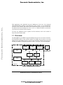
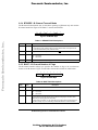
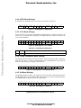
1
Freescale Semiconductor, Inc.
Freescale Semiconductor, Inc...
MC68QH302SUPL/AD
10/97
MC68QH302
Supplement to the MC68302 Integrated Multiprotocol Processor
User’s Manual
For More Information On This Product,
Go to: www.freescale.com
Freescale Semiconductor, Inc...
Freescale Semiconductor, Inc.
Home Page:
www.freescale.com
email:
[email protected]
USA/Europe or Locations Not Listed:
Freescale Semiconductor
Technical Information Center, CH370
1300 N. Alma School Road
Chandler, Arizona 85224
(800) 521-6274
480-768-2130
[email protected]
Europe, Middle East, and Africa:
Freescale Halbleiter Deutschland GmbH
Technical Information Center
Schatzbogen 7
81829 Muenchen, Germany
+44 1296 380 456 (English)
+46 8 52200080 (English)
+49 89 92103 559 (German)
+33 1 69 35 48 48 (French)
[email protected]
Japan:
Freescale Semiconductor Japan Ltd.
Headquarters
ARCO Tower 15F
1-8-1, Shimo-Meguro, Meguro-ku
Tokyo 153-0064, Japan
0120 191014
+81 2666 8080
[email protected]
Asia/Pacific:
Freescale Semiconductor Hong Kong Ltd.
Technical Information Center
2 Dai King Street
Tai Po Industrial Estate,
Tai Po, N.T., Hong Kong
+800 2666 8080
[email protected]
For Literature Requests Only:
Freescale Semiconductor
Literature Distribution Center
P.O. Box 5405
Denver, Colorado 80217
(800) 441-2447
303-675-2140
Fax: 303-675-2150
LDCForFreescaleSemiconductor
@hibbertgroup.com
Information in this document is provided solely to enable system and software
implementers to use Freescale Semiconductor products. There are no express or
implied copyright licenses granted hereunder to design or fabricate any integrated
circuits or integrated circuits based on the information in this document.
Freescale Semiconductor reserves the right to make changes without further notice to
any products herein. Freescale Semiconductor makes no warranty, representation or
guarantee regarding the suitability of its products for any particular purpose, nor does
Freescale Semiconductor assume any liability arising out of the application or use of
any product or circuit, and specifically disclaims any and all liability, including without
limitation consequential or incidental damages. “Typical” parameters which may be
provided in Freescale Semiconductor data sheets and/or specifications can and do
vary in different applications and actual performance may vary over time. All operating
parameters, including “Typicals” must be validated for each customer application by
customer’s technical experts. Freescale Semiconductor does not convey any license
under its patent rights nor the rights of others. Freescale Semiconductor products are
not designed, intended, or authorized for use as components in systems intended for
surgical implant into the body, or other applications intended to support or sustain life,
or for any other application in which the failure of the Freescale Semiconductor product
could create a situation where personal injury or death may occur. Should Buyer
purchase or use Freescale Semiconductor products for any such unintended or
unauthorized application, Buyer shall indemnify and hold Freescale Semiconductor
and its officers, employees, subsidiaries, affiliates, and distributors harmless against all
claims, costs, damages, and expenses, and reasonable attorney fees arising out of,
directly or indirectly, any claim of personal injury or death associated with such
unintended or unauthorized use, even if such claim alleges that Freescale
Semiconductor was negligent regarding the design or manufacture of the part.
For More Information On This Product,
Go to: www.freescale.com
Freescale Semiconductor, Inc.
CONTENTS
Freescale Semiconductor, Inc...
Paragraph
Number
1.1
1.2
2.1
2.1.1
2.1.2
2.2
2.2.1
2.2.2
2.3
2.4
2.5
2.6
2.6.1
2.6.2
2.6.3
2.6.4
2.6.5
2.6.6
2.6.6.1
2.6.7
2.6.7.1
2.6.8
2.6.9
2.6.10
2.6.11
2.6.12
2.6.13
2.6.14
2.7
2.8
2.8.1
2.8.2
2.8.3
2.8.4
2.8.5
2.9
Title
Page
Number
Overview..................................................................................................................1
Features ....................................................................................................................2
Dual-Port RAM Map ...............................................................................................3
Non-QH Mode Parameter RAM Map .................................................................4
QH Mode Parameter RAM Map..........................................................................5
Global QH Parameters .............................................................................................7
Global QH Mode .................................................................................................7
QH Type and Revision Number ..........................................................................7
B1-Channel Parameter RAM...................................................................................8
B2-Channel Parameter RAM.................................................................................10
D-Channel Parameter RAM...................................................................................13
Channel Parameter Descriptions............................................................................14
RSTATEÑReceive Internal State .....................................................................14
T_MODEÑTransmit Mode ..............................................................................16
TSTATEÑTransmit Internal State....................................................................16
BTMODEÑB-Channel Transmit Mode ...........................................................17
BNOFÑB-Channel Number of Flags ...............................................................17
B_STAT1ÑB-Channel Receiver Status ...........................................................18
B-Channel-Overrun and B-Channel-Receiver-Valid Flags...........................18
B_STAT2ÑB-Channel Transmitter Status .......................................................19
B-Channel-Underrun and B-Channel-Transmitter-Valid Flags ....................19
RBASE and TBASEÑDescriptor Table Base Addresses.................................20
TBDPTR and RBDPTRÑTx/Rx Buffer Descriptor Pointers ...........................20
TFCR and RFCRÑData Buffer Function Code Registers................................20
MRBLRÑMaximum Receive Buffer Length Register.....................................20
C_MASK_L/HÑConstant for CRC Check.......................................................21
T_F_MASK and R_F_MASKÑTx/Rx Framer Bit Masks...............................21
Other Channel Parameters .................................................................................21
Non-QH Channel Parameter RAM........................................................................22
SCC Mode Register (SCM) ...................................................................................23
HDLC Mode Settings ........................................................................................23
UART Mode Settings ........................................................................................24
V.110 Mode Settings .........................................................................................24
Totally Transparent Mode Settings....................................................................24
QH Mode Settings .............................................................................................24
QH302 Buffer Descriptor (BD) Structure..............................................................25
Contents
For More Information On This Product,
Go to: www.freescale.com
iii
Freescale Semiconductor, Inc.
CONTENTS
Freescale Semiconductor, Inc...
Paragraph
Number
2.10
2.11
2.12
2.13
2.13.1
2.13.2
2.14
2.15
2.16
2.16.1
2.17
2.18
Title
Page
Number
QH302 Tx Buffer Descriptors for HDLC/Transparent Mode ...............................26
QH302 Rx Buffer Descriptors for HDLC/Transparent Mode...............................27
QH-Mode SCC1 Event Register (SCCE1)............................................................29
Channel Host Commands ......................................................................................30
B-Channel Host Commands ..............................................................................31
D-Channel Host Commands..............................................................................31
QH Parameters Initialization Summary.................................................................32
QH302 HDLC Differences....................................................................................33
QH302 UART Protocol .........................................................................................34
QH302 UART Parameter RAM Map................................................................34
QH Mode Hardware Initialization.........................................................................35
QH302 ISDN BRI Performance ............................................................................36
MC68QH302 Supplement to MC68302 UserÕs Manual
For More Information On This Product,
Go to: www.freescale.com
Freescale Semiconductor, Inc.
ILLUSTRATIONS
Freescale Semiconductor, Inc...
Figure
Number
1
2
3
4
5
6
7
8
9
10
11
12
13
14
15
16
17
18
19
20
21
22
23
24
25
26
Title
Page
Number
MC68QH302 Block Diagram .............................................................................................1
Full ISDN Basic Rate Interface Using the QH302 .............................................................2
D-Channel and B2-Channel Parameter Swapping..............................................................5
Global QH Mode Register ..................................................................................................7
QH Type and Revision Number .........................................................................................8
RSTATE for HDLC/Transparent Channels......................................................................14
RSTATE for UART Channels ..........................................................................................16
TSTATE Register .............................................................................................................16
BTMODE Byte .................................................................................................................17
BNOF Byte .......................................................................................................................17
B_STAT1 Byte .................................................................................................................18
B_STAT2 Byte .................................................................................................................19
Data Buffer Function Code Registers ...............................................................................20
Framer Bit Mask ...............................................................................................................21
SCM Register....................................................................................................................23
SCM Register in HDLC Mode .........................................................................................23
SCM Register in UART Mode .........................................................................................24
SCM Register in V.110 Mode ..........................................................................................24
SCM Register in Transparent Mode .................................................................................24
SCM Register in QH Mode...............................................................................................24
Buffer Descriptor Format..................................................................................................25
SCC Buffer Descriptor Memory Structure .......................................................................26
Tx Buffer Descriptor Status and Control ..........................................................................26
Rx Buffer Descriptor Status and Control..........................................................................27
SCCE1 Register ................................................................................................................29
Host Command Register ...................................................................................................30
Illustrations
For More Information On This Product,
Go to: www.freescale.com
Freescale Semiconductor, Inc...
Freescale Semiconductor, Inc.
MC68QH302 Supplement to MC68302 UserÕs Manual
For More Information On This Product,
Go to: www.freescale.com
Freescale Semiconductor, Inc.
TABLES
Freescale Semiconductor, Inc...
Table
Number
1
2
3
4
5
6
7
8
9
10
11
12
13
14
15
16
17
18
19
20
21
22
23
24
25
26
27
28
29
30
31
32
33
34
Title
Page
Number
System RAM Map ..............................................................................................................3
Non-QH Mode Parameter RAM Map.................................................................................4
B2-Channel Parameter Location.........................................................................................6
D-Channel Parameter Location...........................................................................................6
QH Mode Parameter RAM Map.........................................................................................6
Global QH Mode Field Descriptions ..................................................................................7
QH Type and Revision Number Field Descriptions ...........................................................8
B1-Channel Parameter RAM..............................................................................................8
B2-Channel Fixed-Address Parameters............................................................................10
B2-Channel Rx Swapped Parameters ...............................................................................11
B2-Channel Tx Swapped Parameters ...............................................................................12
D-Channel Rx Swapped Parameters.................................................................................13
D-Channel Tx Swapped Parameters .................................................................................14
RSTATE Field Descriptions for HDLC/Transparent Channels .......................................15
RSTATE Field Descriptions for UART Channels............................................................16
TSTATE Field Descriptions .............................................................................................16
BTMODE Field Descriptions ...........................................................................................17
BNOF Field Descriptions .................................................................................................17
B_STAT1 Field Descriptions ...........................................................................................18
B_STAT2 Field Descriptions ...........................................................................................19
C_MASK_H/L Constants .................................................................................................21
T_F_MASK and R_F_MASK Field Descriptions............................................................21
Non-QH Channel Parameter RAM...................................................................................22
SCM Field Descriptions....................................................................................................23
V.110 Mode RVD Description .........................................................................................24
Tx Status and Control Field Descriptions.........................................................................27
Rx Status and Control Field Descriptions.........................................................................28
SCCE1 Field Descriptions ................................................................................................29
QH Mode Opcodes for the Command Register................................................................30
Command Register Channel Numbers for QH and Non-QH Modes ...............................30
B-Channel Host Commands .............................................................................................31
D-Channel Host Commands .............................................................................................31
Parameters to be Initialized before SCC1 Is Enabled.......................................................32
Parameters to be Initialized before Every restart tx..........................................................32
Tables
For More Information On This Product,
Go to: www.freescale.com
Freescale Semiconductor, Inc.
TABLES
Table
Number
Page
Number
Parameters to be Initialized before Every restart rx..........................................................33
UART Parameter RAM ....................................................................................................34
QH302 ISDN BRI Channel Performance .........................................................................36
Freescale Semiconductor, Inc...
35
36
37
Title
MC68QH302 Supplement to MC68302 UserÕs Manual
For More Information On This Product,
Go to: www.freescale.com
Freescale Semiconductor, Inc.
This supplement to the MC68302 Integrated Multiprotocol Processor UserÕs Manual
(MC68302UM/AD) highlights implementation-speciÞc features of the MC68QH302,
referred to as the ÔQH302Õ, and how they differ from the MC68302, referred to as the Ô302Õ.
The MC68302 Integrated Multiprotocol Processor UserÕs Manual should be consulted for
any features not described in this document.
To locate any published errata or updates for this document, refer to the website at
http://www.mot.com/netcomm.
1.1 Overview
The MC68QH302, quad HDLC integrated multiprotocol processor, is based on the threeSCC MC68302 family of chips with the addition of the QH protocol and two extra serial
DMA channels. The QH302 supports a total of four independent communications channels,
handling two HDLC or transparent channels on SCC1; see Figure 1 for a block diagram.
Interrupt
Controllers
General-Purpose
DMA
Channel
3 Timers
4 Chip Selects
Parallel I/O
RAM
+
ROM
68000
System Bus
M68000
Core
20 Address Lines
8/16 Data Lines
8 DMA
Channels
1152 Bytes
Dual-Port
RAM
Peripheral Bus
RISC
Controller
SCC1
(2 Channels)
SCC2
+
SCC3
SCP
+
2 SMCs
MC68QH302
Figure 1. MC68QH302 Block Diagram
MC68QH302 Supplement to the MC68302 UserÕs Manual
For More Information On This Product,
Go to: www.freescale.com
Addendum to 603e User’s Manual
Freescale Semiconductor, Inc...
0
Freescale Semiconductor, Inc.
For external-active ISDN terminal adaptor applications, SCC1 supports both B channels
(B1 and B2), and SCC3 handles the D channel. SCC2 is thus free to carry a UART host
interface, eliminating the need for host-interface glue logic. Figure 2 shows the
implementation of a full ISDN basic rate interface using the QH302.
Freescale Semiconductor, Inc...
B1 + B2
IDL/GCI
SCC1: QH
S/T or U
Host
SI
SCC2: UART
PC
SCC3: HDLC
D
SCP
ISDN Line
Transceiver
MC68QH302
Figure 2. Full ISDN Basic Rate Interface Using the QH302
In non-QH mode, the QH302 can be used in standard 302 applications as well. Note that
the QH302 SCC parameter RAM mapping has been modiÞed requiring corresponding
adjustments in the conÞguration software. See Section 2.7, ÒNon-QH Channel Parameter
RAM.Ó
1.2 Features
Main features of the QH302 and changes relative to the standard 302 follow:
¥
Supports two independent communications channels using SCC1
¥
Allows independent connection/disconnection for individual B channels
¥
Supports HDLC and totally transparent protocols for individual B channels
¥
Allows independent transmit and receive bit-masking for both B channels
¥
Allows ßexible buffer descriptor table placement using the new base address
parameters, RBASE and TBASE
¥
Allows RAM microcode packages
¥
Enables software to distinguish a QH302 from a 302 by use of a revision number
¥
Supports special host commands for the individual B channels
¥
Supports a 64-ms (or longer) DRAM refresh cycle in QH mode
MC68QH302 Supplement to the MC68302 UserÕs Manual
For More Information On This Product,
Go to: www.freescale.com
Freescale Semiconductor, Inc.
¥
In non-QH mode, all three SCCs can be used in standard 302 conÞgurations.
¥
Pin-compatible with the existing TQFP 302 package
Freescale Semiconductor, Inc...
General QH302 changes relative to 302 are as follows:
¥
The X (external buffer) bit of the buffer descriptorÕs status-and-control word is
reserved in QH302.
¥
The LG (Rx frame length violation) indication bit of the buffer descriptor statusand-control word is not supported by the QH302.
¥
BISYNC and DDCMP protocols are not supported by the QH302.
¥
The SCC data synchronization register (DSR) no longer exists.
¥
A part of the B2-channel parameters swap RAM position with the D-channel
parameters when the B2 channel is enabled. The parameter positions swap back
once B2 is disabled.
¥
The HDLC-speciÞc parameter RAM of a B channel occupies a larger address space
in the QH302.
2.1 Dual-Port RAM Map
The QH302 internal 1176-byte dual-port RAM has 576 bytes of usable system RAM and
576 bytes of parameter RAM.
The system RAM map of the QH302 is unchanged. It may be used to hold special RAM
microcode packages, buffer descriptor tables, or other user-deÞned structures. Table 1
shows the system RAM map.
Table 1. System RAM Map
Base1 Offset
Width
000–0x23F
576 bytes
0x240–0x3FF
Description
User data memory, microcode, and buffer descriptors
Reserved—not implemented
1
Note: As defined in the BAR (base address register).
The parameter RAM map, on the other hand, has changed. In non-QH (3-channel) mode,
the mapping change accounts for QH302-speciÞc global parameters and more ßexible
buffer descriptor placement. In QH mode, the QH protocol remaps the parameter RAM to
accommodate the four serial channels.
MC68QH302 Supplement to the MC68302 UserÕs Manual
For More Information On This Product,
Go to: www.freescale.com
Freescale Semiconductor, Inc.
2.1.1 Non-QH Mode Parameter RAM Map
Freescale Semiconductor, Inc...
In non-QH mode, the QH302Õs parameter RAM map reßects QH302-speciÞc needs and the
added buffer descriptor ßexibility gained with RBASE and TBASE. Buffer descriptor areas
are no longer dedicated to a particular SCC. SCC parameter areas start at the same
locations.
QH302-speciÞc parameters, such as the global QH mode and the QH type and revision
number, start at offset 0x660. Table 2 shows the parameter RAM map for non-QH
operation.
Table 2. Non-QH Mode Parameter RAM Map
Base1 Offset
Width
0x400–0x47F
64 words
Buffer descriptors
0x480–0x4BF
32 words
SCC1 parameter RAM
0x4C0–0x4FF
Description
Reserved—not implemented
0x500–0x56F
56 words
Buffer descriptors
0x570–0x57F
8 words
Buffer descriptors/DRAM refresh parameters
0x580–0x5BF
32 words
SCC2 parameter RAM
0x5C0–0x5FF
Reserved—not implemented
0x600–0x65F
48 words
Buffer descriptors
0x660
Word
Global QH mode
0x662–0x665
2 words
Reserved for internal HW use
0x666
0x668
0x66A
0x66C
0x66E
0x67A
0x67C
0x67E
Word
Word
Word
Word
6 words
Word
Word
Word
SMC1 Rx buffer descriptor
SMC1 Tx buffer descriptor
SMC2 Rx buffer descriptor
SMC2 Tx buffer descriptor
SMC1–SMC2 internal use
SCP Rx/Tx buffer descriptor
SCC1–SCC3 BERR (bus error) channel number
QH type and revision number
0x680–0x6AB
22 words
SCC3 parameter RAM
0x6AC–0x6BF
10 words
Buffer descriptors
0x6C0–0x7FF
Reserved—not implemented
1
Note: As defined in the BAR (base address register).
MC68QH302 Supplement to the MC68302 UserÕs Manual
For More Information On This Product,
Go to: www.freescale.com
Freescale Semiconductor, Inc.
2.1.2 QH Mode Parameter RAM Map
Freescale Semiconductor, Inc...
The QH302Õs parameter RAM has been remapped to accommodate QH mode. To
implement the three channels of ISDN and a UART host channel all running on three SCCs,
part of the B2-channel parameters are juggled with the D-channel parameters.
The B2-channel parameters are broken into three areasÑtwo are Þxed-address while the
third swaps back and forth with the D-channel parameters as B2 is enabled and disabled.
Figure 3 shows the swapping, moving from left to right when B2 is enabled, and back again
when B2 is disabled.
QH Mode Parameter RAM
Map with B2 Stopped
0x400
B1 Parameter RAM
QH Mode Parameter RAM
Map with B2 Running
B2 enabled
B1 Parameter RAM
0x410
0x410
Buffer Descriptors
0x480
Buffer Descriptors
0x480
B2 disabled
B1 Parameter RAM
0x4C0
Reserved
B1 Parameter RAM
Reserved
0x500
D Parameter RAM
0x52C
0x530
Buffer Descriptors
Buffer Descriptors
SCC2 Parameter RAM
SCC2 Parameter RAM
0x580
0x600
0x580
Reserved
Reserved
B2 Fixed Param RAM
B2 Fixed Param RAM
Buffer Descriptors
Buffer Descriptors
Other Registers
Other Registers
0x610
0x660
0x680
0x6AC
0x6C0
0x4C0
0x500
B2 Parameter RAM
0x52C
0x530
0x5AC
0x400
0x5AC
0x600
0x610
D Parameter RAM
B2 Parameter RAM
B2 Fixed Param RAM
B2 Fixed Param RAM
Reserved
Reserved
0x800
0x660
0x680
0x6AC
0x6C0
0x800
Figure 3. D-Channel and B2-Channel Parameter Swapping
MC68QH302 Supplement to the MC68302 UserÕs Manual
For More Information On This Product,
Go to: www.freescale.com
Freescale Semiconductor, Inc.
Table 3 shows the B2-parameter location depending on the activation status of the B2 and
D channels.
Table 3. B2-Channel Parameter Location
Freescale Semiconductor, Inc...
Status of B2
D Stopped
D Running
B2 stopped
0x500–0x52B
0x500–0x52B
B2 running
0x680–0x6AB
Indeterminate
Note: The fixed-address parameters also need to be initialized.
Table 4 shows the D-channel parameter locations depending on the activation status of the
B2 and D channels.
Table 4. D-Channel Parameter Location
Status of B2
D Stopped
D Running
B2 stopped
0x680–0x6AB
0x680–0x6AB
B2 running
0x500–0x52B
Indeterminate
Table 5 shows the QH-mode channel parameter mapping. Note the two highlighted
swapping areas starting at offsets 0x500 and 0x680.
Table 5. QH Mode Parameter RAM Map
Base1 Offset
Description
0x400–0x40F
B1-channel parameter RAM
0x410–0x47F
Buffer descriptors
0x480–0x4BF
B1-channel parameter RAM
0x4C0–0x4FF
Reserved—not implemented
0x500–0x52B
B2-channel parameter RAM (with B2 stopped)
0x52C–0x52F
Reserved—not implemented
0x530–0x56F
Buffer descriptors
0x570–0x57F
Buffer descriptors/DRAM refresh parameters
0x580–0x5AB
SCC2 parameter RAM
0x5AC–0x5FF
Reserved—not implemented
0x600–0x60F
B2-channel fixed-address parameter RAM
0x610–0x65F
Buffer descriptors
0x660–0x67F
(same as corresponding segment in Table 2)
0x680–0x6AB
D-channel parameter RAM (with B2 stopped)
D-channel parameter RAM (with B2 running)
B2-channel parameter RAM (with B2 running)
MC68QH302 Supplement to the MC68302 UserÕs Manual
For More Information On This Product,
Go to: www.freescale.com
Freescale Semiconductor, Inc.
Table 5. QH Mode Parameter RAM Map (Continued)
Base1 Offset
0x6AC–0x6BF
B2-channel fixed-address parameter RAM
0x6C0–0x7FF
Reserved—not implemented
Note:
Freescale Semiconductor, Inc...
Description
1As
defined in the BAR (base address register).
2.2 Global QH Parameters
The QH302 has two QH-speciÞc global parametersÑglobal QH mode and QH type and
revision number.
2.2.1 Global QH Mode
Global QH mode is a memory-mapped register for setting up QH operation. The user must
initialize it before enabling any of the SCCs. Figure 4 shows the bit Þelds and Table 6
describes them.
.
Base + 0x660
15
14
13
12
11
10
9
8
7
6
5
4
3
2
1
0
0
0
0
0
0
0
0
0
0
0
0
0
0
0
FRS
QH
Figure 4. Global QH Mode Register
Table 6. Global QH Mode Field Descriptions
Bit(s)
Name
Description
15–2
—
For internal use—must be initialized to zero.
1
FRS
First time for QH
0 QH protocol over SCC1 has already started.
1 First time to start QH protocol over SCC1 transmitter.
Must be set by the user only before enabling SCC1 or after hardware underrun. Should not be
set when B1- and/or B2-channel/s was/were stopped using STOP TX.
Valid only if QH mode is selected. Set by the user and cleared by the QH302.
0
QH
QH mode
0 Non-QH mode. QH protocol is disabled—SCC1 functions as in 302 operation.
1 QH mode. QH protocol is enabled.
Must be set even if the QH protocol is not currently running but will in the future.
2.2.2 QH Type and Revision Number
QH type and revision number is initialized by the CPM after a hardware reset or a CPM
reset command. It holds the chip type and the internal revision code number. Software can
use the type to distinguish between a 302 and a QH302. Figure 5 shows the bit Þelds and
Table 7 describes them.
QH type and revision number should be initialized to 0x8002 for the Þrst QH302 revision.
MC68QH302 Supplement to the MC68302 UserÕs Manual
For More Information On This Product,
Go to: www.freescale.com
Freescale Semiconductor, Inc.
Base + 0x67E
15
14
13
12
11
10
9
8
7
6
5
4
Type
0
0
0
0
0
0
0
0
0
0
0
3
2
1
0
Rev
Figure 5. QH Type and Revision Number
Table 7. QH Type and Revision Number Field Descriptions
Freescale Semiconductor, Inc...
Bit(s)
Name
Description
15
Type
Chip type
0 302 chip
1 QH302 chip
14–4
—
For internal use—must be initialized to zero
3–0
Rev
Internal revision number
2.3 B1-Channel Parameter RAM
The B1-channel parameter RAM is deÞned in Table 8. Boldfaced parameters are initialized
or used by the host, but must not be changed while the channel is running; see Section 2.6,
ÒChannel Parameter Descriptions,Ó when initializing parameters. Non-boldfaced
parameters are for internal use and should not be changed. ModiÞcation of either B
channelsÕ parameters should be done only when the channel is stopped or before SCC1 is
enabled.
Table 8. B1-Channel Parameter RAM
Base1 Offset
Name
Width
Description
0x400
R_F_DATA
Word
Rx framer data byte (internal)
0x402
F_D_O
Word
Rx/Tx framer data out (also DTSCC)
0x404
R_F_MASK
Byte
Rx framer mask byte
0x405
F_CTR
Byte
Framer internal counter
0x406
TUNPACK
Word
Unpack a word to 2 bytes
0x408
B_STAT1
Byte
B-channel Rx mode & status (internal)
0x409
BNOF
Byte
B-channel number of flags and internal parameters
0x40A
B_STAT2
Byte
B-channel Tx mode & status (internal)
0x40B
BTMODE
Byte
B-channel mode & status (user-defined mode bits)
0x40C
RTEMP
Word
Rx temp
0x40E
NFC
Word
Number-of-flags counter (internal)
0x480
RFCR
Byte
Rx function code
0x481
TFCR
Byte
Tx function code
MC68QH302 Supplement to the MC68302 UserÕs Manual
For More Information On This Product,
Go to: www.freescale.com
Freescale Semiconductor, Inc.
Table 8. B1-Channel Parameter RAM (Continued)
Freescale Semiconductor, Inc...
Base1 Offset
Name
Width
Description
0x482
MRBLR
Word
Maximum receive buffer length
0x484
RBASE
Word
Rx buffer descriptor table base address
0x486
RBDPTR
Word
Rx buffer descriptor pointer
0x488
RBPTR
2 words
Rx internal data pointer
0x48C
RBCNT
Word
Rx internal byte count
0x48E
RCRC
2 words
Temp receive CRC
0x492
C_MASK_L
Word
Constant CRC mask low word
0x494
C_MASK_H
Word
Constant CRC mask high word
0x496
RSTATE
Word
Rx internal state
0x498
TSTATE
Word
Tx internal state
0x49A
TBDPTR
Word
Tx buffer descriptor pointer
0x49C
TBPTR
2 words
Tx internal data pointer
0x4A0
TBCNT
Word
Tx internal byte count
0x4A2
TTEMP
Word
Tx temp
0x4A4
TCRC
2 words
Temp transmit CRC
0x4A8
TBASE
Word
Tx buffer descriptor table base address
0x4AA
T_MODE
Word
Tx mode
0x4AC
TFLGIDL
Word
Tx frame separator (internal)
0x4AE
TTOPTMP
Word
Tx top temporary (internal)
0x4B0
R_F_POST
Byte
Rx framer post byte (internal)
0x4B1
R_F_PRE
Byte
Rx framer pre byte (internal)
0x4B2
R_F_STAT
Word
Rx framer state
0x4B4
T_F_DATA
Byte
Tx framer data byte
0x4B5
T_F_POST
Byte
Tx framer post byte (internal)
0x4B6
T_F_STAT
Word
Tx framer state
0x4B8
T_F_MASK
Byte
Tx framer mask byte
0x4BA
F_TMPM
Word
Framer internal temporary storage for mask
0x4BC
T_F_PRE
Word
Tx framer pre byte
RPACK
Word
Pack 2 bytes into 1 word
0x4BE
Note: 1As defined in the BAR (base address register).
MC68QH302 Supplement to the MC68302 UserÕs Manual
For More Information On This Product,
Go to: www.freescale.com
Freescale Semiconductor, Inc.
2.4 B2-Channel Parameter RAM
There are 2 types of B2-channel parametersÑswapped and Þxed-address. The Þxedaddress B2-channel parameters are deÞned in Table 9.
Table 9. B2-Channel Fixed-Address Parameters
Freescale Semiconductor, Inc...
Base1 Offset
Name
Width
Description
0x600
R_F_DATA
Word
Rx framer data (internal) byte
0x602
F_D_O
Word
Rx/Tx framer data out (also DTSCC)
0x604
R_F_MASK
Byte
Rx framer mask byte
0x605
F_CTR
Byte
Framer internal counter
0x606
TUNPACK
Word
Unpack a word to 2 bytes
0x608
B_STAT1
Byte
B-channel Rx mode & status
0x609
BNOF
Byte
B-channel number of flags and internal parameters
0x60A
B_STAT2
Byte
B-channel Tx mode & status
0x60B
BTMODE
Byte
B-channel mode & status (user-defined mode bits)
0x60C
RTEMP
Word
Rx temp
0x60E
NFC
Word
Number-of-flags counter (internal)
0x6AC
TFLGIDL
Word
Tx frame separator (internal)
0x6AE
TTOPTMP
Word
Tx Top temporary (internal)
0x6B0
R_F_POST
Byte
Rx framer post byte (internal)
0x6B1
R_F_PRE
Byte
Rx framer pre byte (internal)
0x6B2
R_F_STAT
Word
Rx framer state
0x6B4
T_F_DATA
Byte
Tx framer data byte
0x6B5
T_F_POST
Byte
Tx framer post byte (internal)
0x6B6
T_F_STAT
Word
Tx framer state
0x6B8
T_F_MASK
Byte
Tx framer mask byte
0x6BA
F_TMPM
Word
Framer internal temporary storage for mask.
0x6BC
T_F_PRE
Word
Tx framer pre byte
RPACK
Word
Pack 2 bytes into 1 word
0x6BE
Note: 1As defined in the BAR (base address register).
MC68QH302 Supplement to the MC68302 UserÕs Manual
For More Information On This Product,
Go to: www.freescale.com
Freescale Semiconductor, Inc.
The swapped B2-channel parameters are further divided into receive (Rx) and transmit (Tx)
areas. Table 10 shows the Rx-channel parameter locations when the B2 receiver is running
or stopped. See Section 2.6.6, ÒB_STAT1ÑB-Channel Receiver Status,Ó for information on
determining the receiverÕs status. Note that any modiÞcation of parameters should be done
only when the channel is stopped or before the SCC is enabled.
Freescale Semiconductor, Inc...
Table 10. B2-Channel Rx Swapped Parameters
Base1 Offset
(B2 Stopped)2
Base1 Offset
(B2 Running)3
0x500
0x680
RFCR
Byte
Rx function code
0x501
0x681
TFCR
Byte
Tx function code
0x502
0x682
MRBLR
Word
Maximum receive buffer length
0x504
0x684
RBASE
Word
Rx buffer descriptor table base address
0x506
0x686
RBDPTR
Word
Rx buffer descriptor pointer
0x508
0x688
RBPTR
2 words
Rx internal data pointer
0x50C
0x68C
RBCNT
Word
Rx internal byte count
0x50E
0x68E
RCRC
2 words
Temp receive CRC
0x512
0x692
C_MASK_L
Word
Constant CRC mask low word
0x514
0x694
C_MASK_H
Word
Constant CRC mask high word
0x516
0x696
RSTATE
Word
Rx internal state
Name
Width
Description
Notes:
1As
defined in the BAR (base address register)
2Parameter
3Unsafe
location when updating Rx values
location for updating—read-only
MC68QH302 Supplement to the MC68302 UserÕs Manual
For More Information On This Product,
Go to: www.freescale.com
Freescale Semiconductor, Inc.
Table 11 shows the Tx-channel parameter locations when the B2 transmitter is running or
stopped. See Section 2.6.7, ÒB_STAT2ÑB-Channel Transmitter Status,Ó for information
on determining the transmitterÕs status.
Freescale Semiconductor, Inc...
Table 11. B2-Channel Tx Swapped Parameters
Base1 Offset
(B2 Stopped)2
Base1 Offset
(B2 Running)3
0x518
0x698
TSTATE
Word
Tx internal state
0x51A
0x69A
TBDPTR
Word
Tx buffer descriptor pointer
0x51C
0x69C
TBPTR
2 words
Tx internal data pointer
0x520
0x6A0
TBCNT
Word
Tx internal byte count
0x522
0x6A2
TTEMP
Word
Tx temp
0x524
0x6A4
TCRC
2 words
Temp transmit CRC
0x528
0x6A8
TBASE
Word
Tx buffer descriptor table base address
0x52A
0x6AA
T_MODE
Word
Tx mode
Name
Width
Description
Notes:
1As
defined in the BAR (base address register)
2Parameter
3Unsafe
location when updating Tx values
location for updating—read-only
MC68QH302 Supplement to the MC68302 UserÕs Manual
For More Information On This Product,
Go to: www.freescale.com
Freescale Semiconductor, Inc.
2.5 D-Channel Parameter RAM
All the D-channel parameters are swapped. Their location depends on whether the B2
channel is running or not. The receiver parameters are shown in Table 12.
Boldfaced parameters are initialized or used by the host and must not be changed while the
channel is operating. Other parameters are for internal use and should not be changed.
Freescale Semiconductor, Inc...
Table 12. D-Channel Rx Swapped Parameters
Base1 Offset
(B2 Stopped)2
Base1 Offset
(B2 Running)3
0x680
0x500
Name
RFCR
Width
Byte
Description
Rx function code
0x681
0x501
TFCR
Byte
Tx function code
0x682
0x502
MRBLR
Word
Maximum receive buffer length
0x684
0x504
RBASE
Word
Rx buffer descriptor table base address
0x686
0x506
RBDPTR
Word
Rx buffer descriptor pointer
0x688
0x508
RBPTR
2 words
Rx internal data pointer
0x68C
0x50C
RBCNT
Word
Rx internal byte count
0x68E
0x50E
RCRC
2 words
Temp receive CRC
0x692
0x512
C_MASK_L
Word
Constant CRC mask low word
0x694
0x514
C_MASK_H
Word
Constant CRC mask high word
0x696
0x516
RSTATE
Word
Rx internal state
Notes:
1As
defined in the BAR (base address register)
2Rx
parameter location when B2 Rx channel is disabled or after a reset
3Rx
parameter location when B2 Rx channel is enabled
MC68QH302 Supplement to the MC68302 UserÕs Manual
For More Information On This Product,
Go to: www.freescale.com
Freescale Semiconductor, Inc.
The transmitter parameters are shown in Table 13.
Freescale Semiconductor, Inc...
Table 13. D-Channel Tx Swapped Parameters
Base1 Offset
(B2 Stopped)2
Base1 Offset
(B2 Running)3
0x698
0x518
TSTATE
Word
Tx internal state
0x69A
0x51A
TBDPTR
Word
Tx buffer descriptor pointer
0x69C
0x51C
TBPTR
2 Words
Tx internal data pointer
0x6A0
0x520
TBCNT
Word
Tx internal byte count
0x6A2
0x522
TTEMP
Word
Tx temp
0x6A4
0x524
TCRC
2 Words
Temp transmit CRC
0x6A8
0x528
TBASE
Word
Tx buffer descriptor table base address
0x6AA
0x52A
T_MODE
Word
Tx mode
Name
Width
Description
Notes:
1As
defined in the BAR (base address register)
2Tx
parameter location when B2 Tx channel is disabled
3Tx
parameter location when B2 Tx channel is enabled
2.6 Channel Parameter Descriptions
This section describes the channel parameters the user must initialize before a channel is
enabled. Any active channel must Þrst be stopped before updating parameters.
2.6.1 RSTATEÑReceive Internal State
RSTATE must be initialized by the user. Its bit-Þeld deÞnitions depend on the
communications mode selected. Figure 6 shows the Þelds for HDLC or transparent
channels; Table 14 describes these Þelds for QH and non-QH mode operations.
15
14
13
12
11
10
9
8
7
6
MODE
CRC
0
REVD
B-CH
0
0
0
1
D-CH
5
4
3
PAGE
Figure 6. RSTATE for HDLC/Transparent Channels
MC68QH302 Supplement to the MC68302 UserÕs Manual
For More Information On This Product,
Go to: www.freescale.com
2
1
MSNUM
0
Freescale Semiconductor, Inc.
Table 14. RSTATE Field Descriptions for HDLC/Transparent Channels
Freescale Semiconductor, Inc...
Bit(s)
Name
QH Mode (QH = 1)
Non-QH Mode (QH = 0)
15
MODE
0 HDLC mode
1 Transparent mode
Must be programmed to match the mode
selected in the SCC mode register (SCM)
14
CRC
0 CRC-16
1 CRC-32
Must be programmed to match the corresponding
bit in the SCC mode register (SCM)
13
—
12
REVD
0 Receiving LSB first
1 Receiving MSB first—illegal for HDLC
Must be programmed to match the corresponding
bit in the SCC Mode register (SCM)
11
B-CH
B channel in QH mode
0 Not used for B channel
1 Used for B channel
Must be cleared
10–8
—
For internal use—must be initialized to zero
7
—
For internal use—must be initialized to one
6
D-CH
D channel in QH mode
0 Not used for D channel
1 Used for D channel
5–4
PAGE
Page selection
00
B1 channel
01
SCC2 (for UART channel)
10
B2 channel or D channel
00
01
10
Serial number
1001
B1 or B2 channel selected
1011
SCC2 (for UART channel)
1101
D channel
1001
1011
1101
3–0
MSNUM
For internal use—must be initialized to zero
Must be cleared
SCC1
SCC2
SCC3
SCC1
SCC2
SCC3
MC68QH302 Supplement to the MC68302 UserÕs Manual
For More Information On This Product,
Go to: www.freescale.com
Freescale Semiconductor, Inc.
Figure 7 and Table 15 show the RSTATE Þelds for UART channels.
15
14
13
12
11
10
9
8
7
6
0
0
0
0
0
0
0
0
0
0
5
4
3
2
PAGE
1
0
MSNUM
Figure 7. RSTATE for UART Channels
Freescale Semiconductor, Inc...
Table 15. RSTATE Field Descriptions for UART Channels
Bit(s)
Name
15–6
—
5–4
PAGE
3–0
MSNUM
QH Mode (QH = 1)
Non-QH Mode (QH = 0)
For internal use—must be initialized to zero
Page selection—must use SCC2
01
SCC2
00
01
10
SCC1
SCC2
SCC3
Serial number—must use SCC2
1011
SCC2
1001
1011
1101
SCC1
SCC2
SCC3
2.6.2 T_MODEÑTransmit Mode
T_MODE is internal-use only but must be initialized to the same initial value as RSTATE.
2.6.3 TSTATEÑTransmit Internal State
TSTATE must be initialized by the user. Figure 8 and Table 16 show the bit Þelds.
15
14
13
12
11
10
9
8
7
6
0
0
0
0
0
0
0
0
0
0
5
4
3
PAGE
2
1
MSNUM
Figure 8. TSTATE Register
Table 16. TSTATE Field Descriptions
Bits
Name
15–6
—
5–4
PAGE
3–0
MSNUM
QH Mode (QH = 1)
Non-QH Mode (QH = 0)
For internal use—must be initialized to zero
Page selection
00
B1 channel
01
SCC2
10
B2 or D channel
00
01
10
Serial number
1000
B1 or B2 channel
1010
SCC2
1100
D channel
1000
1010
1100
SCC1
SCC2
SCC3
SCC1
SCC2
SCC3
MC68QH302 Supplement to the MC68302 UserÕs Manual
For More Information On This Product,
Go to: www.freescale.com
0
Freescale Semiconductor, Inc.
2.6.4 BTMODEÑB-Channel Transmit Mode
The B-channel transmit mode byte is valid when operating in QH mode only and contains
B-channel mode bits. Figure 9 and Table 17 describe the bit Þelds.
7
6
FLG
TIDL
5
4
3
2
PAGE
1
0
MSNUM
Freescale Semiconductor, Inc...
Figure 9. BTMODE Byte
Table 17. BTMODE Field Descriptions
Bit(s)
Name
Description
7
FLG
Flag mode—send FLAG or IDLE characters between HDLC frames
0 Send IDLEs (‘0xFF’) between frames—must be selected when in transparent mode
1 Send FLAG characters (‘0x7E’) between frames
6
TIDL
Programmed to be the complement of the FLG bit (FLG)
5–4
PAGE
Page selection
00
B1 channel
10
B2 channel
3–0
MSNUM
Serial number should always be programmed to 0b1000.
2.6.5 BNOFÑB-Channel Number of Flags
The B-channel number-of-ßags byte speciÞes the number of ßags to be sent between
frames on the B channels. Figure 10 and Table 18 show the bit Þelds for initialization.
7
6
00
5
4
3
2
PAGE
1
0
NOF
Figure 10. BNOF Byte
Table 18. BNOF Field Descriptions
Bit(s)
Name
Description
7–6
—
For internal use—must be initialized to zero
5–4
PAGE
Page selection
00
B1 channel
10
B2 channel
3–0
NOF
Minimum number of flags between or before frames, 0 to 15.
For transparent mode, NOF must be zero so that the closing flag of one frame will be
followed by the opening flag of the next frame.
In HDLC mode, when NOF = 0, the closing flag of one frame and the opening flag of the
next frame overlap; only one “shared flag” is transmitted between consecutive frames.
MC68QH302 Supplement to the MC68302 UserÕs Manual
For More Information On This Product,
Go to: www.freescale.com
Freescale Semiconductor, Inc.
2.6.6 B_STAT1ÑB-Channel Receiver Status
B_STAT1 contains B-channel receiver status bits and internal-use bits. After reset or a
hardware overrun error, the user must clear this byte for both B channels. After this initial
clearing, however, the user should access this byte using host commands only; see Section
2.13.1, ÒB-Channel Host Commands,Ó for more information on how host commands affect
B-channel status bits. Figure 11 shows the Þelds and Table 19 describes them.
Freescale Semiconductor, Inc...
7
6
5
4
000000
3
2
1
0
BOV
BRV
Figure 11. B_STAT1 Byte
Table 19. B_STAT1 Field Descriptions
Bit(s)
Name
Description
7–2
—
For internal use—must be initialized to zero
1
BOV
B channel receiver overrun—must be initialized to zero
0 No overrun error
1 Overrun error
0
BRV
B channel receiver valid—must be initialized to zero
0 B channel receiver disabled
1 B channel receiver enabled
2.6.6.1 B-Channel-Overrun and B-Channel-Receiver-Valid Flags
B_STAT1[BOV] reports overrun errors and B_STAT1[BRV] reßects the channelÕs
activation status.
When the host does not prepare an empty buffer descriptor for incoming data, a receiver
error (RXE) interrupt is triggered and the overrunning B channelÕs B_STAT1[BOV] is set,
disabling the receiver. The user must determine which B channel has overrun by polling
both B channelsÕ B_STAT1[BOV] and then issue STOP RX for that channel. STOP RX clears
B_STAT1[BRV]. Note that both B channels could overrun simultaneously as in the case of
a hardware overrun.
It is the user's responsibility to re-initialize the channel parameters and then issue
reactivating the channel. RESTART RX clears B_STAT1[BOV] and sets
B_STAT1[BRV].
RESTART RX,
MC68QH302 Supplement to the MC68302 UserÕs Manual
For More Information On This Product,
Go to: www.freescale.com
Freescale Semiconductor, Inc.
2.6.7 B_STAT2ÑB-Channel Transmitter Status
Freescale Semiconductor, Inc...
B_STAT2 contains B-channel transmitter status bits and internal-use bits. After reset, the
user must clear this byte for both B channels. After this initial clearing, however, the user
should access this byte using host commands only; see Section 2.13.1, ÒB-Channel Host
Commands,Ó for more information on how host commands affect B-channel status bits.
Figure 12 shows the Þelds and Table 20 describes them.
7
6
5
4
3
2
1
0
0
BUN
0
BTV
0
0
0
0
Figure 12. B_STAT2 Byte
Table 20. B_STAT2 Field Descriptions
Bit(s)
Name
Description
7
—
For internal use—must be initialized to zero
6
BUN
B channel transmitter underrun—must be initialized to zero
0 No underrun error
1 Underrun error
5
—
For internal use—must be initialized to zero
4
BTV
B channel transmitter valid—must be initialized to zero
0 B channel transmitter disabled
1 B channel transmitter enabled
3–0
—
For internal use—must be initialized to zero
2.6.7.1 B-Channel-Underrun and B-Channel-Transmitter-Valid Flags
B_STAT2[BUN] reports underrun errors and B_STAT2[BTV] reßects the channelÕs
activation status.
When the host does not prepare the necessary data for the complete transmission of the
current frame, the RISC controller underruns. The controller then sets B_STAT2[BUN],
disabling the underrunning B channelÕs transmitter, and signals the host with a transmitter
error (TXE) interrupt. An abort sequence followed by idle characters (high voltage) will be
automatically sent.
The user must determine which B channel has underrun by polling both B channelsÕ
B_STAT2[BUN] and then issue STOP TX for that channel. STOP TX clears B_STAT2[BUN].
Note that both B channels could underrun simultaneously as in the case of a hardware
underrun.
It is the user's responsibility to re-initialize the channel parameters and then issue
reactivating the channel. RESTART TX clears B_STAT1[BUN] and sets
B_STAT1[BTV].
RESTART TX,
MC68QH302 Supplement to the MC68302 UserÕs Manual
For More Information On This Product,
Go to: www.freescale.com
Freescale Semiconductor, Inc.
If an underrun exception occurs in a B channel programmed for ßag mode (see Section
2.6.4, ÒBTMODEÑB-Channel Transmit Mode,Ó) the B channel will go into idle mode, that
is, transmit idle Ô1Õs.
Freescale Semiconductor, Inc...
2.6.8 RBASE and TBASEÑDescriptor Table Base Addresses
RBASE and TBASE allow the user to program the base address of buffer descriptor tables
in the dual-port RAM. Each channel has its own pairÑan RBASE to point to its Rx buffer
descriptor table and a TBASE for its Tx descriptor table. In other words, unlike the 302, the
QH302Õs descriptor tables are not locked into a Þxed position and thus are no longer limited
to holding only 8 buffer descriptors.
The user must initialize RBASE and TBASE before enabling the channel. They must be
divisible by 8 and range from 0 to 0x800 to Þt within the dual-port RAM. Furthermore,
RBASE and TBASE should be chosen to ensure descriptor tables of different channels do
not overlap.
2.6.9 TBDPTR and RBDPTRÑTx/Rx Buffer Descriptor Pointers
Rx buffer descriptor pointer (RBDPTR) and Tx buffer descriptor pointer (TBDPTR) point
to the buffer descriptors currently being used by the receive and transmit channels,
respectively. They should be initialized to the values of RBASE and TBASE, respectively.
2.6.10 TFCR and RFCRÑData Buffer Function Code Registers
The function code registers deÞne the address space of the receive (RFCR) and transmit
(TFCR) data buffers. These registers must be initialized before enabling the SCC. Bits 3Ð0
and bit 7 are internal-use only but must be initialized to 0; see Figure 13. Note that setting
FC[2Ð0] to 0b111 will cause a conßict with the interrupt acknowledge cycle. See the
MC68302 userÕs manual for more information on function codes.
7
6
5
4
3
2
1
0
0
FC2
FC1
FC0
0
0
0
0
Figure 13. Data Buffer Function Code Registers
2.6.11 MRBLRÑMaximum Receive Buffer Length Register
The MRBLR sets the maximum number of bytes that the QH302 will write to a receiver
buffer before moving to the next. The QH302 may write fewer bytes to the buffer if an endof-frame or error occurs. MRBLR must hold an even number greater than zero.
MC68QH302 Supplement to the MC68302 UserÕs Manual
For More Information On This Product,
Go to: www.freescale.com
Freescale Semiconductor, Inc.
2.6.12 C_MASK_L/HÑConstant for CRC Check
The C_MASK constant is used for the CRC check. The values for CRC16/CRC32 modes
are shown in Table 21. For software testing, an incorrect initialization can be used to force
a receive-CRC error.
Table 21. C_MASK_H/L Constants
Freescale Semiconductor, Inc...
CRC Mode
C_MASK_H
C_MASK_L
CRC16
(This field is ignored.)
$F0B8
CRC32
0x20E3
$DEBB
2.6.13 T_F_MASK and R_F_MASKÑTx/Rx Framer Bit Masks
T_F_MASK and R_F_MASK select what bits are active in the B channel. Any combination
of the 8 bits may be chosen. Figure 14 shows the Þelds for the framer masks; Table 22
describes the masking for sending and receiving. These parameters must be initialized if
QH mode is selected.
15
14
13
12
11
10
9
8
M0
M1
M2
M3
M4
M5
M6
M7
Figure 14. Framer Bit Mask
Table 22. T_F_MASK and R_F_MASK Field Descriptions
Bit(s)
Mask Bit(s)
15
M[0]
14–8
M[1–7]
T_F_MASK
R_F_MASK
0 Mask the corresponding TXD bit— ‘1’ is
driven on the transmit line.
1 Bit ‘transmitted—data will be transmitted.
0 Mask the corresponding RXD bit—the bit
is not received.
1 Bit received— data will be shifted into the
receiver.
Note: The bit order in this entry is opposite to the bit order in the SIMASK register.
2.6.14 Other Channel Parameters
All other parameters do not need to be accessed by the user in normal operationÑthey only
need to be initialized every time the QH receiver or transmitter channel is restarted. Section
2.14, ÒQH Parameters Initialization Summary,Ó lists initial values for these parameters. The
initial value of parameters not described is unimportant.
MC68QH302 Supplement to the MC68302 UserÕs Manual
For More Information On This Product,
Go to: www.freescale.com
Freescale Semiconductor, Inc.
2.7 Non-QH Channel Parameter RAM
Table 23 describes the parameter RAM for SCCs operating in non-QH mode. If QH mode
is selected, this parameter RAM only applies to SCC2.
For full descriptions of these parameters, see Section 2.6, ÒChannel Parameter
Descriptions.Ó
Freescale Semiconductor, Inc...
Table 23. Non-QH Channel Parameter RAM
SCC Base Offset
Name
Width
Description
0x80
RFCR
Byte
Rx function code
0x81
TFCR
Byte
Tx function code
0x82
MRBLR
Word
Maximum receive buffer length
0x84
RBASE
Word
Rx buffer descriptor table base address
0x86
RBDPTR
Word
Rx internal buffer pointer
0x88
RBPTR
2 words
Rx internal data pointer
0x8C
RBCNT
Word
Rx internal byte count
0x8E
RCRC
2 words
Temp receive CRC
0x92
C_MASK
2 words
Constant CRC mask
0x96
RSTATE
Word
Rx internal state
0x98
TSTATE
Word
Tx internal state
0x9A
TBDPTR
Word
Tx internal buffer pointer
0x9C
TBPTR
2 words
Tx internal data pointer
0xA0
TBCNT
Word
Tx internal byte count
0xA2
TTEMP
Word
Tx temp
0xA4
TCRC
2 words
Temp transmit CRC
0xA8
TBASE
Word
Tx buffer descriptor table base address
0xAA
T_MODE
Word
Tx mode
MC68QH302 Supplement to the MC68302 UserÕs Manual
For More Information On This Product,
Go to: www.freescale.com
Freescale Semiconductor, Inc.
2.8 SCC Mode Register (SCM)
The QH302 supports Þve protocolsÑHDLC, UART, V.110, transparent, and QH. Only
SCC1 can run the QH protocol. The SCC mode registers (SCM) determine the protocol to
be run for each SCC. Figure 15 shows the SCM register.
15
14
13
12
11
10
9
8
7
6
Freescale Semiconductor, Inc...
Mode-Specific Bits
5
4
Diag[1:0]
3
2
ENR
ENT
1
0
Mode[1:0]
Figure 15. SCM Register
SCM[5Ð0] are common to each protocol while the mode-speciÞc bits SCM[15Ð6] vary
according to the protocol selected in SCM[1Ð0]. This register is cleared by reset. See
Table 24 for Þeld descriptions.
Table 24. SCM Field Descriptions
Bits
Name
15–6
Description
—
Mode-specific bits
5–4
Diag[1:0]
Diagnostic mode (same as 302)
3
ENR
Enable receiver
2
ENT
Enable transmitter
1–0
Mode[1:0]
Channel mode
00 = HDLC
01 = UART
10 = V.110
11 = Totally transparent/QH (for SCC1 only)
Descriptions of the speciÞc mode settings follow.
2.8.1 HDLC Mode Settings
In HDLC mode, the SCM register is the same as in the 302; see Figure 16.
15
14
13
NOF[3:0]
12
11
10
9
8
7
6
C32
FSE
0
RTE
FLG
ENC
5
4
Diag[1:0]
3
2
ENR
ENT
Figure 16. SCM Register in HDLC Mode
MC68QH302 Supplement to the MC68302 UserÕs Manual
For More Information On This Product,
Go to: www.freescale.com
1
0
00
Freescale Semiconductor, Inc.
2.8.2 UART Mode Settings
In UART mode, the SCM register is the same as in the 302; see Figure 17.
15
14
TPM[1:0]
13
12
RPM
PEN
11
10
UM[1:0]
9
8
7
6
FRZ
CL
RTSM
SL
5
4
Diag[1:0]
3
2
ENR
ENT
1
0
01
Figure 17. SCM Register in UART Mode
Freescale Semiconductor, Inc...
2.8.3 V.110 Mode Settings
The V.110 mode is selected by programming the SCM register as in Figure 18. The V.110
mode may be activated when operating in non-QH mode only. Table 25 describes the
reverse-data Þeld RVD.
15
14
13
12
11
10
9
8
7
6
0
0
0
0
0
1
0
RVD
0
0
5
4
Diag[1:0]
3
2
ENR
ENT
1
0
10
Figure 18. SCM Register in V.110 Mode
Table 25. V.110 Mode RVD Description
Bit
Name
8
RVD
Description
Reverse data. Reverses the reception bit order. Should be set for regular V.110 operation.
2.8.4 Totally Transparent Mode Settings
The transparent mode settings are shown in Figure 19 and only apply to SCC2 and SCC3.
Note that since there is no data synchronization register, synchronization can be achieved
from an external pin or by using the serial interface.
15
14
13
12
11
10
9
8
7
6
0
1
1
RVD
0
0
0
0
0
0
5
4
Diag[1:0]
3
2
ENR
ENT
1
0
11
Figure 19. SCM Register in Transparent Mode
2.8.5 QH Mode Settings
The QH mode applies to SCC1 only and must be selected for SCC1 when QH operation is
needed. QH mode can be selected for IDL or GCI modes only, without any bit masking by
the SIMASK register. Figure 20 shows the QH settings.
15
14
13
12
11
10
9
8
7
6
0
1
1
0
0
0
0
0
0
0
5
4
Diag[1:0]
3
2
ENR
ENT
Figure 20. SCM Register in QH Mode
MC68QH302 Supplement to the MC68302 UserÕs Manual
For More Information On This Product,
Go to: www.freescale.com
1
0
11
Freescale Semiconductor, Inc.
2.9 QH302 Buffer Descriptor (BD) Structure
The QH302Õs overall buffer descriptor structure is the same as in the 302; however, the
status-and-control word has been modiÞed. The 302Õs X (external buffer) bit and the LG
(Rx frame length violation) indication bit are no longer supported in the QH302Õs buffer
descriptor status-and-control word. Figure 21 shows the buffer descriptor format.
Freescale Semiconductor, Inc...
15
14
13
12
11
10
9
8
7
6
5
+0
+2
Status and Control
Data Length
+4
+6
Buffer Pointer (24 bits used; upper 8 bits must be 0)
4
3
2
1
0
Figure 21. Buffer Descriptor Format
All the buffer descriptors of a particular channel are combined into a single buffer
descriptor table. A buffer descriptor table forms a circular queue with a programmable
length. The user programs the tablesÕ base addresses using RBASE and TBASE to place
the tables in any unused portion of the dual-port RAM, including any unused parameter
RAM. The data buffers are free to go anywhere in the address space; however, internal
placement of buffers will not result in better performance. Figure 22 shows the BD memory
structure.
MC68QH302 Supplement to the MC68302 UserÕs Manual
For More Information On This Product,
Go to: www.freescale.com
Freescale Semiconductor, Inc.
External RAM
Dual-Port RAM
Freescale Semiconductor, Inc...
SCC Buffer
Descriptor
Table Pointers
(Rx/Tx BDPTR)
Data Buffer
Data Buffer
RBASE/TBASE
Buffer Descriptors
SCC Buffer
Descriptor
Table
Status and Control
Data Length
Buffer Pointer
Figure 22. SCC Buffer Descriptor Memory Structure
2.10 QH302 Tx Buffer Descriptors for
HDLC/Transparent Mode
The transmitter uses the Tx BD to report information about the transmitted data associated
with each BD. The Þrst word contains status and control information and is shown in
Figure 23. Table 26 describes the status-and-control bit Þelds.
+0
15
R
14
—
13
W
12
I
11
L
10
TC
9
—
8
—
7
—
6
—
5
—
4
—
3
—
Figure 23. Tx Buffer Descriptor Status and Control
MC68QH302 Supplement to the MC68302 UserÕs Manual
For More Information On This Product,
Go to: www.freescale.com
2
—
1
UN
0
CT
Freescale Semiconductor, Inc.
Table 26. Tx Status and Control Field Descriptions
Freescale Semiconductor, Inc...
Bit(s)
Name
Description
15
R1
Ready
0 =The data buffer is not ready for sending. Cleared by the transmitter after the buffer has been
fully sent or an error condition occurs.
1=The data buffer is ready for sending, but has not yet been fully sent. The host should not
modify any field of this BD after setting this bit.
14
—
Reserved
13
W1
Wrap
0 = Not the last BD in the Tx BD table.
1 = The last BD in the Tx BD table.
12
I1
Interrupt.
0 = No TXB interrupt is generated after this buffer was transmitted.
1= The TXB bit in the event register (SCCE) will be set.
11
L1
Last
0 = Not the last buffer in the frame.
1 = The last buffer in the frame.
10
TC1
Transmit CRC. Valid only when the last (L) bit is set.
0 = Do not send CRC after the last byte is sent.
1 = Send the CRC after the last byte is sent.
9–2
—
Reserved
1
UN2
Underrun. A transmitter underrun occurred. Not set for B channels.
0
CT2
Clear-to-send lost. The CTS for an NMSI channel, or L1GR (layer-1 grant) in IDL/GCI for the D
channel, was lost during frame transmission.
Notes:
1Written
2Status
by the user before the buffer is sent
flag set by the transmitter after the entire data buffer has been sent
2.11 QH302 Rx Buffer Descriptors for
HDLC/Transparent Mode
The receiver uses the Rx buffer descriptor to report information about the received data.
Figure 24 shows the status-and-control word. Table 27 describes the status-and-control bit
Þelds.
+0
15
14
13
12
11
10
9
8
7
6
5
4
3
2
1
0
E
—
W
I
L
F
—
—
—
—
—
NO
AB
CR
OV
CD
Figure 24. Rx Buffer Descriptor Status and Control
MC68QH302 Supplement to the MC68302 UserÕs Manual
For More Information On This Product,
Go to: www.freescale.com
Freescale Semiconductor, Inc.
Table 27. Rx Status and Control Field Descriptions
Freescale Semiconductor, Inc...
Bit(s)
Name
Description
15
E1
Empty
0 = The data buffer associated with this BD has been filled with data, or data reception was
aborted due to error condition. The host is free to examine or write to any field of the BD.
1 = The data buffer associated with this BD is empty. The host should not write to any field of
this BD after it sets this bit. Cleared by the receiver when the buffer is full or frame reception
was stopped due to an end-of-frame or an error.
14
—
Reserved
13
W1
Wrap
0 = Not the last BD in Rx BD table
1 = The last BD in Rx BD table
12
I1
Interrupt
0 = The RXB bit is not set after this buffer is used, but RXF operation remains unaffected.
1 = The RXB bit in the event register (SCCE) will be set.
11
L2
Last. Set by the receiver when this buffer is the last in a frame, implying the end-of-frame
reception due to a closing flag, in HDLC mode, or an error.
0 = Not the last buffer in the frame.
1 = The last buffer in the frame.
10
F2
First. Set by the receiver when this buffer is the first in a frame.
0 = Not the first buffer in the frame.
1 = The first buffer in the frame.
9–5
—
Reserved
4
NO2
Rx non-octet-aligned. A frame that contained a number of bits not exactly divisible by 8 was
received. The last data word written into a non-octet BD is undefined and should be discarded
by software.
3
AB2
Rx abort sequence. At least seven consecutive ‘1’s occurred during frame reception. Valid for
HDLC mode only.
2
CR2
CRC error. The frame contains a CRC error.
1
OV2
Overrun. A receiver overrun occurred. Not set for B channels.
0
CD2
Carrier detect lost. The carrier detect (CD) signal was negated during frame reception. Valid for
NMSI channels only.
Notes:
1Written
by the user before the buffer is linked to the Rx buffer descriptor table
2Updated
by the receiver after the data has been placed into its buffer
MC68QH302 Supplement to the MC68302 UserÕs Manual
For More Information On This Product,
Go to: www.freescale.com
Freescale Semiconductor, Inc.
2.12 QH-Mode SCC1 Event Register (SCCE1)
Freescale Semiconductor, Inc...
In QH mode, the SCC1 event register (SCCE1) reports events occurring in both B channels.
When SCCE1 reports an event, the user must check each B channelsÕ Rx/Tx status registers
B_STAT1/2 to determine which B channel reported. Figure 25 shows SCCE1.
7
6
5
4
3
2
1
0
—
—
—
TXE
RXF
RXE
TXB
RXB
Figure 25. SCCE1 Register
Each bit of the event register can generate an interrupt maskable by the SCC mask register
(SCCM). SCCE1[7Ð5] should always be masked for the B channels. Table 28 describes the
SCCE1 Þelds.
Table 28. SCCE1 Field Descriptions
Bits
Name
Description
7–5
—
Should be masked in the SCC1 mask register; their value is undefined in QH mode.
4
TXE
Tx error. An underrun error has occurred. Once detected, the B channel ends buffer
transmission and sends an abort sequence. The transmitter sets B_STAT2[BUN] and sets
SCCE1[TXE]. Note that the BUN bit can be set in both channels.
Upon a TXE event, the host should read each B channels’ B_STAT2[BUN] to determine
which channel(s) underran. For each B channel whose BUN bit is set, the host should issue
STOP TX, initialize the transmit parameters (see Section 2.14, “QH Parameters Initialization
Summary”), and then issue RESTART TX to restart the B channe(s)l.
3
RXF
Rx frame. A RXF event indicates a complete frame has been received in one or both B
channels. Host must check each BD table to determine which channel(s) has a new frame.
2
RXE
Rx error. A RXE event indicates a busy condition or an overrun has been detected by one
or both B channels. The receiver stops and sets the channel’s B_STAT1[BOV].
Upon a RXE event, the host should read each B channels’ B_STAT1[BOV] to determine
which channel(s) are reported. For each B channel whose BOV bit is set, the host should
issue STOP RX, initialize the receive parameters (see Section 2.14, “QH Parameters
Initialization Summary”), and then issue RESTART RX to restart the channel.
1
TXB
Tx buffer. A TXB event indicates a buffer has been sent in either B1 or in B2. When
enabled, the TXB interrupt is generated when the last data of the buffer is written to the
FIFO, but not yet sent. This is opposite to the 302 behavior for the last buffer in a frame.
0
RXB
Rx buffer. An RXB event indicates that a buffer has been received either in B1 or in B2.
MC68QH302 Supplement to the MC68302 UserÕs Manual
For More Information On This Product,
Go to: www.freescale.com
Freescale Semiconductor, Inc.
2.13 Channel Host Commands
Freescale Semiconductor, Inc...
The host issues commands to the CPM through the command register. The host should set
the FLG bit when sending a command. After executing the command, the CPM clears the
FLG bit to signal command completion. The host should poll the FLG bit before issuing
the next command. A reset clears the command register. Figure 26 shows the Þelds of the
command register.
Base + 0x860
7
6
RST
GCI
5
4
OPCODE
3
2
—
CH. NUM.
1
0
FLG
Figure 26. Host Command Register
For non-QH operation and for non-QH or NMSI channels, the QH302Õs command register
functions the same as in the 302. The RST and GCI commands are also the same. In QH
mode, however, the channel numbers and opcodes are interpreted differently. Table 29
shows the QH-mode interpretation of the opcodes; Table 30 shows the difference in channel
numbers between QH and non-QH modes.
Table 29. QH Mode Opcodes for the Command Register
Opcode
B Channel Command
D Channel Command
00
STOP TX
STOP TX
01
RESTART TX
RESTART TX
10
STOP RX
ENTER HUNT MODE
11
RESTART RX
Reserved
Table 30. Command Register Channel Numbers for QH and Non-QH Modes
Channel Number
Non-QH Mode
QH Mode
00
SCC1
B1 Channel
01
SCC2
SCC2
10
SCC3
D Channel
11
Reserved
B2 Channel
MC68QH302 Supplement to the MC68302 UserÕs Manual
For More Information On This Product,
Go to: www.freescale.com
Freescale Semiconductor, Inc.
2.13.1 B-Channel Host Commands
The B-channel host commands are described in Table 31. Note that the B-channel receivers
do not have an ENTER HUNT MODE option and must be explicitly stopped and restarted.
Table 31. B-Channel Host Commands
Freescale Semiconductor, Inc...
B-Channel
Command
Description
STOP TX
stops a Tx B channel. It must be issued after a transmit error or if the B-channel parameters
need to be modified. STOP TX clears B_STAT2[BTV] of the designated B channel, invalidating the
channel. The B channel transmission is aborted and idle characters (‘1’s) are sent. The host can now
modify the parameters. In HDLC mode, an HDLC abort pattern is sent.
Note: If the STOP TX is for a B channel programmed in flag mode (see Section 2.6.4, “BTMODE—BChannel Transmit Mode”), the B channel goes into idle mode, sending idle characters (‘1’s) following
the abort sequence. After executing RESTART TX, the channel starts from its initial state as
programmed in the BTMODE register.
RESTART TX
RESTART TX
STOP RX
STOP RX
RESTART RX
RESTART RX
STOP TX
initiates transmission on a B channel following a STOP TX command or an underrun error.
The command sets B_STAT2[BTV] and clears B_STAT2[BUN] of the designated B channel. The
channel is now considered running (prohibiting parameter modification), and the first Tx buffer
descriptor is polled.
stops a Rx B channel. It must be issued after a receive error or if the B-channel parameters
need to be modified. STOP RX clears the B_STAT1[BRV] of the designated B channel, invalidating the
channel. The host can now modify the parameters (see Section 2.14, “QH Parameters Initialization
Summary,” for B-channel parameter initialization).
initiates reception on a B channel, setting B_STAT1[BRV] of the designated B channel.
The channel is now considered running, prohibiting parameter modification. The receiver searches for
the start-of-frame condition on the receive data line to fill the first Rx buffer with data.
2.13.2 D-Channel Host Commands
The D-channel host commands are described in Table 32.
Table 32. D-Channel Host Commands
D-Channel
Command
Description
stops the channel. It must be issued after a transmit error or if the channel parameters need
to be modified. Channel transmission is aborted and idle characters (‘1’s) are sent. The host can now
modify the parameters (see Section 2.14, “QH Parameters Initialization Summary,” for parameter
initialization). In HDLC mode, an HDLC abort pattern is sent.
Note: As long as the B2 channel is running, the D-channel parameters will remain in their swapped
position.
STOP TX
STOP TX
RESTART TX
RESTART TX initiates transmission on the channel following a STOP TX command or an underrun error.
The channel is now considered running (prohibiting parameter modification), and the first Tx buffer
descriptor is polled.
ENTER HUNT
ENTER HUNT MODE
MODE
is generally used to abort reception of the current frame and restart reception of
the next frame. It is the same as in the 302.
MC68QH302 Supplement to the MC68302 UserÕs Manual
For More Information On This Product,
Go to: www.freescale.com
Freescale Semiconductor, Inc.
2.14 QH Parameters Initialization Summary
Freescale Semiconductor, Inc...
All parameters must be initialized after every software or hardware reset and before
enabling any serial channel, but only some of them should be initialized before every
RESTART. See Table 33, Table 34, and Table 35 for the initialization of the B channels when
operating in QH mode. Initialization of all other serial channels parameters, boldfaced
parameters in Section 2.7, ÒNon-QH Channel Parameter RAM,Ó should be initialized as in
the 302 with the addition of RSTATE and T_MODE.
Each channelsÕ parameters can be modiÞed only while the channel is stopped or disabled.
Table 33. Parameters to be Initialized before SCC1 Is Enabled
Parameter Name
Value
T_F_DATA
0xFF
T_F_STAT
For B1: 0xE008
For B2: 0xE028
T_F_POST
0x80
Global_QH_Mode
See Section 2.2.1, “Global QH Mode.”
B_STAT1
See Section 2.6.6, “B_STAT1—B-Channel Receiver Status.”
B_STAT2
See Section 2.6.7, “B_STAT2—B-Channel Transmitter Status.”
RSTATE
See Section 2.6.1, “RSTATE—Receive Internal State.”
T_F_MASK
See Section 2.6.13, “T_F_MASK and R_F_MASK—Tx/Rx Framer Bit Masks.”
R_F_MASK
See Section 2.6.13, “T_F_MASK and R_F_MASK—Tx/Rx Framer Bit Masks.”
Table 34. Parameters to be Initialized before Every RESTART
Parameter Name
HDLC Mode Value
TX
Transparent Mode Value
TFLGIDL
0x7E7E
0xFFFF
TTOPTMP
Flag mode: 0x8000
Idle mode: 0x0000
0x0000
BNOF
See Section 2.6.5, “BNOF—B-Channel Number of Flags.”
BTMODE
See Section 2.6.4, “BTMODE—B-Channel Transmit Mode.”
TSTATE
See Section 2.6.3, “TSTATE—Transmit Internal State.”
TFCR
See Section 2.6.10, “TFCR and RFCR—Data Buffer Function Code Registers.”
TBASE
See Section 2.6.8, “RBASE and TBASE—Descriptor Table Base Addresses.”
TBDPTR
See Section 2.6.9, “TBDPTR and RBDPTR—Tx/Rx Buffer Descriptor Pointers.”
T_MODE
See Section 2.6.2, “T_MODE—Transmit Mode.”
MC68QH302 Supplement to the MC68302 UserÕs Manual
For More Information On This Product,
Go to: www.freescale.com
Freescale Semiconductor, Inc.
Table 35. Parameters to be Initialized before Every RESTART RX
Freescale Semiconductor, Inc...
Parameter Name
HDLC Mode Value
Transparent Mode Value
R_F_STAT
For B1: 0x0000
For B2: 0x0020
For B1: 0x02C0
For B2: 0x02E0
R_F_POST
0x00
R_F_PRE
0x00
RSTATE
See Section 2.6.1, “RSTATE—Receive Internal State.”
RFCR
See Section 2.6.10, “TFCR and RFCR—Data Buffer Function Code Registers.”
RBASE
See Section 2.6.8, “RBASE and TBASE—Descriptor Table Base Addresses.”
RBDPTR
See Section 2.6.9, “TBDPTR and RBDPTR—Tx/Rx Buffer Descriptor Pointers.”
MRBLR
See Section 2.6.11, “MRBLR—Maximum Receive Buffer Length Register.”
C_MASK_L/H
See Section 2.6.12, “C_MASK_L/H—Constant for CRC Check.”
2.15 QH302 HDLC Differences
The QH302 HDLC protocol does not support the following:
¥
Address recognition (no SCC data synchronization register (DSR))
¥
Error statistics counters
¥
Checking of frames that are too long (MFLR).
Additional differences are as follows:
¥
Non-octet frameÑthe last 16 data bits of non-octet frame may be corrupted.
¥
The data-length word of the last Rx buffer descriptor in frame contains the length of
the last buffer only.
¥
IDL/CTS/CD interrupts are not supported for either B channel but are supported for
the QH-HDLC protocol.
¥
Host commands for the B channels can only enable/disable the Rx/Tx channels; see
Section 2.13, ÒChannel Host Commands.Ó
¥
ENTER HUNT MODE does not exist for the B channels. Instead, the user must STOP RX,
update parameters, and then RESTART RX.
¥
After executing a STOP TX instruction for either B channel, the channel enters idle
mode until the RESTART TX instruction is executed.
MC68QH302 Supplement to the MC68302 UserÕs Manual
For More Information On This Product,
Go to: www.freescale.com
Freescale Semiconductor, Inc.
¥
B channels acknowledge the transmission when the data enters the SCC1Õs FIFO
buffer and not when actually sent.
¥
The QH302Õs serial performance is degraded by 10% relative to the 302; see
Appendix A, ÒSCC Performance,Ó of the MC68302 userÕs manual.
Freescale Semiconductor, Inc...
2.16 QH302 UART Protocol
The QH302Õs UART parameter RAM has been relocated and remapped; otherwise, UART
operation is the same as in the 302. See the latest MC68302 userÕs manual for UART
initialization and operation.
2.16.1 QH302 UART Parameter RAM Map
The QH302Õs UART parameter map is similar to the 302, but parameters were moved to
new offsets; see Table 36. The two new parameters, RBASE and TBASE, allow the user to
place the buffer descriptor tables in any free space in the dual-port RAM; see Section 2.6.8,
ÒRBASE and TBASEÑDescriptor Table Base Addresses.Ó One control character was
removed.
Table 36. UART Parameter RAM
SCC Base Offset
Name
Width
Description
0x80
RFCR
Byte
Rx function code
0x81
TFCR
Byte
Tx function code
0x82
MRBLR
Word
Maximum receive buffer length
0x84
RBASE
Word
Rx buffer descriptor base address
0x86
RBDPTR
Word
Rx internal buffer pointer
0x88
RBPTR
2 Words
Rx internal data pointer
0x8C
RBCNT
Word
Rx internal byte count
0x8E
PAREC
Word
Receive parity error counter
0x90
FRMEC
Word
Receive framing error counter
0x92
NOSEC
Word
Receive noise counter
0x94
BRKEC
Word
Receive break condition counter
0x96
RSTATE
Word
Rx internal state
0x98
TSTATE
Word
Tx internal state
0x9A
TBDPTR
Word
Tx internal buffer pointer
0x9C
TBPTR
2 Words
Tx internal data pointer
0xA0
TBCNT
Word
Tx internal byte count
0xA2
TTEMP
Word
Tx temp
MC68QH302 Supplement to the MC68302 UserÕs Manual
For More Information On This Product,
Go to: www.freescale.com
Freescale Semiconductor, Inc.
Table 36. UART Parameter RAM (Continued)
Freescale Semiconductor, Inc...
SCC Base Offset
Name
Width
Description
0xA4
MAX_IDL
Word
Maximum IDLE characters (Rx)
0xA6
IDLC
Word
Temporary receive IDLE counter
0xA8
TBASE
Word
Tx buffer descriptor base address
0xAA
BRKCR
Word
Break count register (Tx)
0xAC
UADDR1
Word
UART address character 1
0xAE
UADDR2
Word
UART address character 2
0xB0
RCCR
Word
Receive control character register
0xB2
CHARACTER1
Word
Control character 1
0xB4
CHARACTER2
Word
Control character 2
0xB6
CHARACTER3
Word
Control character 3
0xB8
CHARACTER4
Word
Control character 4
0xBA
CHARACTER5
Word
Control character 5
0xBC
CHARACTER6
Word
Control character 6
0xBE
CHARACTER7
Word
Control character 7
2.17 QH Mode Hardware Initialization
The proper initialization order of the internal QH302 modules begins with the external pins,
then the serial interface, and the SCCs last. The following shows the proper hardware
initialization sequence for QH operation:
1. Program the parallel I/O to select the pins needed for the application.
2. Select SCC2 pins for dedicated mode to connect SCC2 to the external pins to operate
as a DTE connection.
3. Program the serial interface registers to conÞgure the serial channel physical
interface:
SIMASK:write 0xFFFF to SIMASK register.
SIMODE: select the IDL/GCI mode using the MS[0,1] bits.
Ñ Route B1 and B2 to SCC1, that is, [B1RB,B1RA] = 01, [B2RB, B2RA] = 01.
Ñ Route D channel to SCC3, that is, [DRB,DRA] = 11 and MSC3 = 0.
Ñ Route SCC2 to the NMSI pins, that is, MSC2 = 1.
Ñ All other bits are user-deÞned.
4. Program the QH parameters in the dual-port RAM.
5. Program SCON1 and SCON3 to 0x3000 to enable operating from the SI clock.
MC68QH302 Supplement to the MC68302 UserÕs Manual
For More Information On This Product,
Go to: www.freescale.com
Freescale Semiconductor, Inc.
6. Program the interrupt controller mask register (IMR) to enable SCC interrupts.
7. Program SCC1 mask register (SCCM1) to enable B-channel interrupts.
Freescale Semiconductor, Inc...
8. Program SCC1 mode register (SCM1) (for both B1and B2 channels) to totally
transparent mode, that is, SCM1 = 0x600F.
9. Program SCC3 mask register (SCCM3) to enable D-channel interrupts.
10. Program SCC3 mode register (SCM3) (D channel) to HDLC/transparent mode (as
in the 302).
11. Program SCC2 mask register (SCCM2) to enable SCC2 interrupts.
12. Program SCON2 to select the clock source for SCC2.
13. Program SCC2 mode register (SCM2) (DTE connection) to
HDLC/transparent/UART mode (as in the 302).
2.18 QH302 ISDN BRI Performance
Channel speeds for a basic rate ISDN interface is shown in Table 37.
Table 37. QH302 ISDN BRI Channel Performance
System Clock
B11
B21
D2
UART3
Autobaud
25 MHz
64 Kbps
64 Kbps
16 Kbps
230 Kbps
115 Kbps
33 MHz
64 Kbps
64 Kbps
16 Kbps
460 Kbps
230 Kbps
Notes:
1HDLC
on SCC1
2HDLC
on SCC3
3SCC2
MC68QH302 Supplement to the MC68302 UserÕs Manual
For More Information On This Product,
Go to: www.freescale.com
Freescale Semiconductor, Inc.
INDEX
RSTATE
HDLC/transparent channels, 14
UART channels, 16
T_F_MASK, 21
T_MODE, 16
TBASE, 20
TBDPTR, 20
TFCR, 20
TSTATE, 16
Commands, channel host, 30
Numerics
Freescale Semiconductor, Inc...
302 differences from QH302, 3, 33
B
B_STAT1 (B-channel receiver status) byte, 18
B_STAT2 (B-channel transmitter status), 19
B1-channel parameter RAM, 8
B2-channel parameter
description, 10
fixed-address parameters, 10
location, 6
Rx swapped parameters, 11
swapping, 5
Tx swapped parameters, 12
B-channel host commands, 31
Block diagram, 1
BNOF (B-channel number of flags) byte, 17
BTMODE (B-channel transmit mode) byte, 17
Buffer descriptors
buffer descriptor structure, 25
Rx buffer descriptor, 27
Tx buffer descriptor, 26
D
Data buffer function code registers (TFCR/RFCR), 20
D-channel parameter
description, 13
host commands, 31
location, 6
Rx swapped parameters, 13
swapping, 5
Tx swapped parameters, 14
Descriptor table base addresses, 20
Differences from 302, 3, 33
Dual-port RAM map, 3
C
F
C_MASK_L/H (constant for CRC check), 21
Changes from 302, 3, 33
Channel host commands, 30
Channel parameters
B_STAT1, 18
B_STAT2, 19
B2-channel parameter swapping, 5
B-channel host commands, 31
BNOF, 17
BTMODE, 17
C_MASK_L/H, 21
D-channel
host commands, 31
parameter swapping, 5
ISDN BRI channel performance, 36
MRBLR, 20
R_F_MASK, 21
RBASE, 20
RBDPTR, 20
RFCR, 20
Features, list, 2
Fixed-address parameter RAM, B2-channel, 10
Flags, B-channel
overrun, 18
receiver-valid, 18
transmitter-valid, 19
underrun, 19
G
Global QH mode
parameters, 7
register, 7
Index
For More Information On This Product,
Go to: www.freescale.com
Freescale Semiconductor, Inc.
Freescale Semiconductor, Inc...
INDEX
H
Q
Hardware initialization, 35
HDLC protocol, 33
HDLC/transparent mode
RSTATE, 14
Rx buffer descriptors, 27
Tx buffer descriptors, 26
Host command register, 30
QH mode
global parameters, 7
hardware initialization, 35
initialization summary, 32
opcodes for command register, 30
parameter RAM map, 5, 6
SCCE1 register, 29
QH type and revision number register, 7
I
Initialization summary
hardware initialization, 35
QH parameters initialization, 32
ISDN basic rate interface, 2
ISDN BRI channel performance, 36
M
Maps
B1-channel parameter RAM map, 8
B2-channel parameter RAM map, 10
D-channel parameter RAM map, 13
dual-port RAM map, 3
non-QH mode parameter RAM map, 4, 22
parameter RAM map, 3
QH mode parameter RAM map, 5, 6
system RAM map, 3
MRBLR (maximum receive buffer length) register, 20
N
Non-QH mode parameter RAM map, 4, 22
O
Opcodes, QH mode opcodes for command register, 30
Overview, 1
P
Parameters
B1-channel parameter RAM map, 8
B2-channel parameter RAM map, 10
D-channel parameter RAM map, 13
global QH parameters, 7
non-QH mode parameter RAM map, 4, 22
parameter swapping
B2-channel, 5
D-channel, 5
QH mode
initialization summary, 32
parameter RAM map, 5, 6
UART protocol RAM map, 34
R
R_F_MASK (Rx framer bit mask), 21
RAM maps
B1-channel, 8
B2-channel, 10
D-channel, 13
dual-port, 3
non-QH mode, 4, 22
parameter RAM map, 3
QH mode, 5, 6
system RAM map, 3
UART RAM maps, 34
RBASE, 20
RBDPTR (Rx buffer descriptor pointer), 20
Registers
global QH mode, 7
host command, 30
MRBLR, 20
QH type and revision number, 7
RFCR, 20
SCCE1, 29
SCM, 23
TFCR, 20
RFCR register, 20
RSTATE (receive internal state)
HDLC/transparent channels, 14
UART channels, 16
Rx buffer descriptors, HDLC/transparent mode, 27
Rx swapped parameter RAM
B2-channel, 11
D-channel, 13
S
SCC buffer descriptor memory structure, 26
SCC mode register, 23
SCCE1 (SCC1 event) register, 29
SCM (SCC mode) register, 23
System RAM map, 3
MC68QH302 Supplement to MC68302 UserÕs Manual
For More Information On This Product,
Go to: www.freescale.com
Freescale Semiconductor, Inc.
INDEX
Freescale Semiconductor, Inc...
T
T_F_MASK (Tx framer bit mask), 21
T_MODE (transmit mode), 16
TBASE, 20
TBDPTR (Tx buffer descriptor pointer), 20
TFCR register, 20
TSTATE (transmit internal state), 16
Tx buffer descriptors, HDLC/transparent mode, 26
Tx swapped parameter RAM
B2-channel, 12
D-channel, 14
U
UART protocol
RAM map, 34
RSTATE, 16
Index
For More Information On This Product,
Go to: www.freescale.com
Freescale Semiconductor, Inc.
Freescale Semiconductor, Inc...
INDEX
MC68QH302 Supplement to MC68302 UserÕs Manual
For More Information On This Product,
Go to: www.freescale.com