1
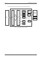
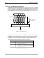
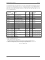
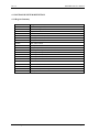
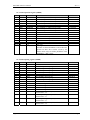
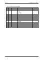
VME64x IP carrier board
Document N°: MANH402-51
TM
MAXVME-6400
User Manual
Version 1.2
MAXVME-6400 User Manual
Rev 1.2
TM
Copyright © 2007 MAX Technologies Inc. All rights reserved, including those to reproduce this publication or parts thereof in
any form without prior written permission from MAX Technologies Inc. Printed in Canada.
MAX Technologies, MAXVME-6400, and the MAX Technologies logo are all trademarks of MAX Technologies Inc. All other
trademarks and registered trademarks are the property of their respective owners.
Changes are periodically made to the information in this document. These changes will be incorporated into new editions of this
document. MAX Technologies may make improvements and/or changes in the products and/or programs described in this
document at any time. MAX Technologies Inc. makes no warranties as to the contents of this manual or the accompanying
software. Although every effort has been made to ensure that the manual is accurate and that the software is reliable, MAX
Technologies Inc. cannot be held responsible for any damages suffered from the use of this product.
How to reach MAX Technologies for Product Support
7005 Taschereau Blvd., Suite 350
Brossard, Quebec
Canada, J4Z 1A7
Tel.: (450) 443-3332
Fax: (450) 443-1618
Toll free: (800) 361-1629
www.maxt.com
Page 2
MAX Technologies
Rev 1.2
MAXVME-6400 User Manual
MAXVME-6400 USER’S MANUAL HISTORY
DOCUMENT REVISION
Details
Logic - Embedded Code
PCB
Revision 1.0
- First Release
Rev 90001
Rev. 1.0
Revision 1.1
Rev 90002
- Added new LED functionality
Rev. 1.0
Revision 1.2
Rev 90002
- Minor syntax corrections
Rev. 1.0
MAX Technologies
Page 3
MAXVME-6400 User Manual
Rev 1.2
Table of Contents
Table of Contents ............................................................................................................................................. 4
CHAPTER 1...................................................................................................................................................... 8
GENERAL INTRODUCTION ........................................................................................................................ 8
1.1 INTRODUCTION...................................................................................................................................... 8
CHAPTER 2.................................................................................................................................................... 10
ON-BOARD HARDWARE SPECIFICATION ............................................................................................ 10
2.1 Timer and Synchronization ...................................................................................................................... 10
2.1.1 System synchronization..................................................................................................................... 10
2.1.1.1 Slave card ................................................................................................................................... 10
2.1.1.2 Master with internal reference card ............................................................................................ 10
2.1.1.3 Master with external reference card ........................................................................................... 10
2.1.1.4 Master with VME_SYSCLK reference card .............................................................................. 11
2.1.1.5 Optional IRIG-B synchronization .............................................................................................. 12
2.1.1.6 Timer synchronization................................................................................................................ 12
2.2 Interrupt Time Tag Fifo............................................................................................................................ 13
2.3 Optional +/-15V DCDC ........................................................................................................................... 13
2.4 Temperature Sensor.................................................................................................................................. 13
CHAPTER 3.................................................................................................................................................... 14
PHYSICAL CONFIGURATION & INSTALLATION ................................................................................ 14
3.1 INTRODUCTION.................................................................................................................................... 14
3.2 Connector, switch and jumper.................................................................................................................. 15
3.2.1 IP position ......................................................................................................................................... 15
3.2.2 VME connector IO assignment ......................................................................................................... 15
3.2.3 J1 - J2 - +/-15V select........................................................................................................................ 16
3.2.4 JP1 ..................................................................................................................................................... 16
3.2.5 JP2 ..................................................................................................................................................... 16
3.2.6 JP3 ..................................................................................................................................................... 16
3.2.7 JP4 ..................................................................................................................................................... 16
3.2.8 Switch S2 – A24-CR/CSR and A16 Address range .......................................................................... 17
3.2.9 SW1-SW7 - Multi-board synchronization port connectors............................................................... 18
3.2.10 Status LED ...................................................................................................................................... 19
CHAPTER 4.................................................................................................................................................... 20
MEMORY & IO MAP ................................................................................................................................... 20
4.1 VME-6400 MEMORY MAP ................................................................................................................... 20
4.1.1 VME6400 IPack & Control register Memory Map........................................................................... 20
4.1.2 VME6400 IPack Memory Access ..................................................................................................... 21
4.1.3 VME6400 Geographical Addressing A16 and CR/CSR A24 memory access.................................. 21
4.2 CONTROL REGISTERS DEFINITION ................................................................................................. 25
4.2.1 Register Summary ............................................................................................................................. 25
4.2.1.1 Interrupt mask register (0x0000) ................................................................................................ 26
4.2.1.2 Interrupt flag register (0x0004) .................................................................................................. 26
4.2.1.3 IP configuration register (0x0008) ............................................................................................. 27
4.2.1.4 General control Register (0x000C) ............................................................................................ 28
4.2.1.5 64-bit timer register (0x0010 and 0x0014)................................................................................. 28
4.2.1.6 64-bit counter value at last IP interrupt (0x0018 and 0x001C) .................................................. 29
4.2.1.7 VME control (0x0020) ............................................................................................................... 30
4.2.1.8 A32_A24_IPMEMCONTROL control register (0x0024) ......................................................... 30
4.2.1.9 Temperature sensor data (0x0028 – 0x002C) ............................................................................ 31
Page 4
MAX Technologies
Rev 1.2
MAXVME-6400 User Manual
4.2.1.10 IRIG-B correlation timer (0x0030-0x0034) .............................................................................31
4.2.1.11 IRIG-B data (0x0038)...............................................................................................................31
4.2.1.12 Model and Revision register (0x003C).....................................................................................32
4.2.1.13 User defined register (0x0070-0x7C) .......................................................................................32
4.2.1.14 User RAM (128 bytes) (0x0080-0x00FC)................................................................................32
CHAPTER 5 ....................................................................................................................................................33
INTERRUPTS................................................................................................................................................33
5.1 VME INTERRUPTS ................................................................................................................................33
CHAPTER 6 ....................................................................................................................................................34
SPECIFICATION...........................................................................................................................................34
6.1 ELECTRICAL..........................................................................................................................................34
6.2 MECHANICAL .......................................................................................................................................34
6.3 ENVIRONEMENTAL .............................................................................................................................34
MAX Technologies
Page 5
MAXVME-6400 User Manual
Rev 1.2
List of Figures
Figure 1-1: MAXVME-6400 Block diagram .........................................................................................................9
Figure 3-1: IP and Switch position.......................................................................................................................14
Figure 3-2: GA base address circuit .....................................................................................................................17
Figure 3-3: SW1 to SW7 circuit...........................................................................................................................18
Page 6
MAX Technologies
Rev 1.2
MAXVME-6400 User Manual
List of Tables
Table 2-1: MAXVME-6400 Synchronization configuration and states...............................................................11
Table 3-1: VME-64x back plane IO (P2) .............................................................................................................15
Table 3-2: VME-64x back plane IO (P0) .............................................................................................................16
Table 3-3: local base address settings...................................................................................................................17
Table 3-4: SW1 to SW7 description.....................................................................................................................18
Table 3-5: LED Definitions..................................................................................................................................19
Table 4-1: VME6400 IPack & Control register Memory Map ............................................................................20
Table 4-2: VME6400 IPack memory, A32 Memory Map....................................................................................21
Table 4-3: VME6400 IPack memory, A24 Memory Map....................................................................................21
Table 4-4a: VME6400, CR...................................................................................................................................22
Table 4-4b: VME6400, CR ..................................................................................................................................23
Table 4-5: VME6400, CSR ..................................................................................................................................24
Table 5-1: Interrupts routing to the VME bus interrupt system. ..........................................................................33
Table 6-1: VME6400 power requirement ............................................................................................................34
Table 6-2: MAXVME-6400 Environmental Specifications.................................................................................34
MAX Technologies
Page 7
MAXVME-6400 User Manual
Rev 1.2
CHAPTER 1
GENERAL INTRODUCTION
1.1 INTRODUCTION
The MAXVME-6400 is an Industry Pack (IP) carrier board designed to be compliant with the VME64x, and supports the A32/A24/A16/D32/D16/D08, single and block access. It supports up to four
single-width IP modules, or 2 double-width IP modules, where every IP bus has its independent 8MHz
or 32 MHz clock.
Features
• 4 single (8 or 16 bit) or 2 double (32 bit) IP sites.
• Per IP selectable operating frequency (8 or 32Mhz) and width (16 or 32 bit), no hold cycle.
• 64-bit timer that can be frequency and phase synchronized between multiple VME-64 carriers and
others MAX Technologies carrier boards.
• Temperature sensor
• IRIG-B circuitry
• Optional +/-15V instead of regular +/-12V on IP modules
• Four status LEDs.
Page 8
MAX Technologies
Rev 1.2
MAXVME-6400 User Manual
The following figure presents the block diagram of the MAXVME-6400 board:
VME64
IP0
VME P2
IP1
VME
Back Plane
Rear I/O
IP2
VME P0
IP3
VME bus
P1/P2
Transceiver
&
Quick Switch
FPGA
IRIG Circuit
(optionnal)
IRIG Signal
Sync In/Out
FLASH/
SDRAM
(optionnal)
DCDC
+/-15V
(optionnal)
VCXO
Figure 1-1: MAXVME-6400 Block diagram
MAX Technologies
Page 9
MAXVME-6400 User Manual
Rev 1.2
CHAPTER 2
ON-BOARD HARDWARE SPECIFICATION
2.1 Timer and Synchronization
The MAXVME-6400 has a 1 us resolution, 64-bit free running counter as main timer. This freerunning counter is accessible via the 64BIT_COUNTER registers.
2.1.1 System synchronization
Many or a single MAXVME-6400 and the IPs on them can have their timer synchronized in phase and
frequency with or without an external reference. To do so, the MAXVME-6400 cards must be daisychained using their input and output synchronization ports (SYNC_IN, SYNC_OUT). The resulting
daisy-chained scheme is used to propagate the reference and synchronization symbols from the first
card of the chain to the last one. This important feature gives the opportunity to have the same timebase over a complete system with a simple coax or twisted pair wire from a MAXVME-6400 to
another.
2.1.1.1 Slave card
The slave state is reached when the card detects reference symbols from a master card on its
SYNC_IN port. The selected reference source must be the SYNC_IN port. The reference source is
selected with REF_SRC bit of the GENERAL_CTRL register (see section 4.2.1.4). In this state
INT_REF of the GENERAL_CTRL register is set to ‘0’ because the clock reference is external.
2.1.1.2 Master with internal reference card
This master state is reached when the card does not detect an external reference or reference symbols
and when the selected reference source is the SYNC_IN port. Then, the card uses its own VCXO for
reference symbol generation on its SYNC_OUT port. Consequently the slave card attached to the
master SYNC_OUT port locks its VCXO to the master VCXO. In this state INT_REF of the
GENERAL_CTRL register is set to ‘1’ because the clock reference is internal.
The VCXO of the master card can be calibrated for a specific operating temperature. Note that the
MAXVME-6400 VCXO has a temperature stability of +/- 25 PPM over all the specified operating
temperature range. The VCXO has a pulling range of +/- 100 PPM. The XO_CAL 8-bit value of the
GENERAL_CTRL register (section 4.4.8) is used to calibrate the VCXO frequency. Writing a value to
those bits will pull the VCXO to a corresponding frequency, 0x00 is pulling the VCXO down to the
slowest frequency and 0xFF is pulling the VCXO up to the highest frequency.
2.1.1.3 Master with external reference card
This master state is reached when the card detects an external 1Mhz clock on its SYNC_IN port but no
reference symbols. The reference source is selected with the REF_SRC bit of the GENERAL_CTRL
register (see section 4.4.8). When a master card detects this reference it automatically locks its onboard VCXO to this external reference. Then the card generates reference symbols on its SYNC_OUT
port. Consequently the slave card attached to the master card SYNC_OUT port locks its VCXO to the
reference too.
An external reference connected to the SYNC_IN port of the master card must meet the following:
1- 1 MHz square wave +/- 100 PPM.
2- TTL level compatible.
3- 40-60% duty cycle.
The difference between reference symbols and an external clock reference is the clock duty cycle.
Page 10
MAX Technologies
Rev 1.2
MAXVME-6400 User Manual
2.1.1.4 Master with VME_SYSCLK reference card
This master state is reached when the external reference source is the VME_SYSCLK. The reference
source is selected with the REF_SRC bit of the GENERAL_CTRL register (see section 4.4.8). The
card locks its on-board VCXO to this external reference. Then the card generates reference symbols on
its SYNC_OUT port. Consequently the slave card attached to the master card SYNC_OUT port locks
its VCXO to that VME_SYSCLK too.
In this state, INT_REF of the GENERAL_CTRL register is set to ‘0’ because the clock reference is
external.
When used, the VME system clock must meet the following:
1- 16 Mhz +/- 100 PPM accuracy
IMPORTANT : Slave state is not possible when the VME system clock is selected as the external
reference, because the card will never detect reference symbols generated by a master card. Only a
desired master card should have the VME system clock as its external reference source.
SYNCHRONIZATION
STATUS
Slave
0 : SYNC_IN port
Master with internal reference
0 : SYNC_IN port
Master with external reference
Master with VME_SYSCLK
reference
0 : SYNC_IN port
1 : VME_SYSCLK
(1)
(2)
(3)
REF_SRC bit (1)
SYNC_IN port
INT_REF bit (2)
SYNC_OUT port of 0 : External Reference
another MAXT
card
No external
1 : VCXO with
XO_CAL
reference detected
External Reference 0 : External Reference
Do not care
0 : External Reference
MSTR_SLA bit (3)
0 : SLAVE
1 : MASTER
1 : MASTER
1 : MASTER
See section 4.2.1.4 GENERAL_CTRL Register, bit 29.
See section 4.2.1.4 GENERAL_CTRL Register, bit 24.
See section 4.2.1.4 GENERAL_CTRL Register, bit 31.
Table 2-1: MAXVME-6400 Synchronization configuration and states
MAX Technologies
Page 11
MAXVME-6400 User Manual
Rev 1.2
2.1.1.5 Optional IRIG-B synchronization
The MAXVME-6400 can also optionally be synchronized on an external IRIG-B signal if your carrier
comes with the IRIG-B decoder circuitry. If so, when the IRIGB_ENABLE bit is activated and the
IRIG-B signal is connected to IRIG-B_IN, the MAXVME-6400 will synchronies its internal clock and
timer on the incoming signal by automatically adjusting the VCXO.
The decoder logic accepts both TTL and standard amplitude-modulated (AM) IRIG-B signal. When
using the TTL input, the 1us synchronicity is exact since the rising edge of the TTL output
corresponds exactly to the Pr point. When using an AM IRIG-B signal, the decoder circuitry and logic
will synchronize on the zero crossing of the beginning of the Pr point of the AM modulated signal.
This zero crossing of the low frequency AM modulated signal is not as accurate as the TTL or 1PPS
signal. So, the user may use a 1PPS signal on the TTL input to improve synchronicity when using the
IRIG-B AM signal or compensate.
Note that when the card is in the SLAVE state, the IRIGB_ENABLE is ignored, and the card is
synchronized with the MASTER card.
Note that the IRIG-B signal should be standard amplitude modulated IRIG-B signals in the range of
0.1 to 10 Vpp. Both, signal and ground, IRIG-B pins must be connected for correct decoding.
The decoded IRIG-B data and the registered value of the 64-bit timer are available for correlation
between the two timing methods. See register section for detail.
2.1.1.6 Timer synchronization
The timer present on some IP modules as well as the 64-bit free running counter of the MAXVME6400 can all be synchronized in phase. The RST_CNT bit of the INTERRUPT_MASKS register
(section 4.2.1.1) resets the free running counter and also sends a 0.125 us low pulse on the IP
STROBE lines that may be used to reset IP modules timers1.
When writing 1 to the RST_CNT bit of the master card, a reset symbol is generated to the
SYNC_OUT port and consequently all over the cards chain. The detection of this reset symbol by the
slave cards resets their free running counter and also sends a 0.125 us low pulse on their IP STROBE
signal.
On a master or a slave card, the SYNC_DONE bit of the GENERAL_CTRL register indicates when
such a timer/counter reset occurred (see section 4.2.1.4).
IMPORTANT: When writing a 1 to the RST_CNT bit of the INTERRUPT_MASKS of a slave card,
no synchronization symbol is generated to the SYNC_OUT port of this card, but it resets the counters
of this card only.
1
All MAX Technologies IP modules support this feature, however it is not specified in the IP specification.
Other manufacturers may not support this feature.
Page 12
MAX Technologies
Rev 1.2
MAXVME-6400 User Manual
2.2 Interrupt Time Tag Fifo
It is possible for the user to obtain the value of the 64BIT_COUNTER register at the time of all the
incoming IP interrupt sources. Activating the INTCNT_enable bit in IP_Configuration register enables
this feature. By doing so, the IP interrupts will only be presented one at a time. The associated countertimer value is available in the INT_COUNT register. If more then one interrupt is received from the IP
modules, the associated counter values are memorized and will be presented once the first interrupt is
cleared. There is no obligation to read the INT_COUNT even if the option is enabled.
2.3 Optional +/-15V DCDC
The MAXVME-6400 is optionally equipped with two DCDC converters, which can provide +/-15V
instead of +/-12V to the IP modules. Those DCDC can provide up to 260mA per output and are
powered by the VME bus 5V. The user can choose +/-15V by setting the J1 and J2 jumpers.
2.4 Temperature Sensor
The MAXVME-6400 is equipped with 4 temperatures sensor, which are place near each IP module
sites, and give the possibility to monitor the temperature of the board during operation. The
temperature is available with a 0.5°C precision. See register section for detail.
MAX Technologies
Page 13
MAXVME-6400 User Manual
Rev 1.2
CHAPTER 3
PHYSICAL CONFIGURATION & INSTALLATION
3.1 INTRODUCTION
This section covers the physical configuration of the MAXVME-6400 board:
•
•
•
•
•
IP position and IO connectors pin-out
Serial port pin-out
VME address range setting dipswitches
Board to board synchronization port connector
Reset button and status LEDs
Figure 3-1: IP and Switch position
Page 14
MAX Technologies
Rev 1.2
MAXVME-6400 User Manual
3.2 Connector, switch and jumper
3.2.1 IP position
Figure 3.1 above shows the position of the 4 IP modules that can support a MAXVME-6400 board.
Single size IPs may use any of the four slots shown. Double size IPs may use slot A&B or C&D.
3.2.2 VME connector IO assignment
The two following table present the IP modules IO connection to the VME connector P0 and P2. Note
that the IOs are connected as indicated in specification “VITA 4.1-1996 ; IP I/O Mapping to
VME64x”.
Row
VME Connector
Position
d
c
a
z
P2
P2
P2
P2
P2
P2
P2
P2
P2
P2
P2
P2
P2
P2
P2
P2
P2
P2
P2
P2
P2
P2
P2
P2
P2
P2
P2
P2
P2
P2
P2
P2
1
2
3
4
5
6
7
8
9
10
11
12
13
14
15
16
17
18
19
20
21
22
23
24
25
26
27
28
29
30
31
32
IPC-IO47
IPC-IO48
IPC-IO50
IPB-IO1
IPB-IO3
IPB-IO4
IPB-IO6
IPB-IO7
IPB-IO9
IPB-IO10
IPB-IO12
IPB-IO13
IPB-IO15
IPB-IO16
IPB-IO18
IPB-IO19
IPB-IO21
IPB-IO22
IPB-IO24
IPB-IO25
IPB-IO27
IPB-IO28
IPB-IO30
IPB-IO31
IPB-IO33
IPB-IO34
IPB-IO36
IPB-IO37
IPB-IO39
IPB-IO40
GND
VPC
IPB-IO42
IPB-IO44
IPB-IO46
IPB-IO48
IPB-IO50
IPA-IO2
IPA-IO4
IPA-IO6
IPA-IO8
IPA-IO10
IPA-IO12
IPA-IO14
IPA-IO16
IPA-IO18
IPA-IO20
IPA-IO22
IPA-IO24
IPA-IO26
IPA-IO28
IPA-IO30
IPA-IO32
IPA-IO34
IPA-IO36
IPA-IO38
IPA-IO40
IPA-IO42
IPA-IO44
IPA-IO46
IPA-IO48
IPA-IO50
3.3V
5V
IPB-IO41
IPB-IO43
IPB-IO45
IPB-IO47
IPB-IO49
IPA-IO1
IPA-IO3
IPA-IO5
IPA-IO7
IPA-IO9
IPA-IO11
IPA-IO13
IPA-IO15
IPA-IO17
IPA-IO19
IPA-IO21
IPA-IO23
IPA-IO25
IPA-IO27
IPA-IO29
IPA-IO31
IPA-IO33
IPA-IO35
IPA-IO37
IPA-IO39
IPA-IO41
IPA-IO43
IPA-IO45
IPA-IO47
IPA-IO49
3.3V
5V
IPC-IO46
GND
IPC-IO49
GND
IPB-IO2
GND
IPB-IO5
GND
IPB-IO8
GND
IPB-IO11
GND
IPB-IO14
GND
IPB-IO17
GND
IPB-IO20
GND
IPB-IO23
GND
IPB-IO26
GND
IPB-IO29
GND
IPB-IO32
GND
IPB-IO35
GND
IPB-IO38
GND
3.3V
GND
Table 3-1: VME-64x back plane IO (P2)
MAX Technologies
Page 15
MAXVME-6400 User Manual
Rev 1.2
Row
VME Connector
P0
P0
P0
P0
P0
P0
P0
P0
P0
P0
P0
P0
P0
P0
P0
P0
P0
P0
P0
Position
1
2
3
4
5
6
7
8
9
10
11
12
13
14
15
16
17
18
19
f
GND
GND
GND
GND
GND
GND
GND
GND
GND
GND
GND
GND
GND
GND
GND
GND
GND
GND
GND
e
IPD-IO5
IPD-IO10
IPD-IO15
IPD-IO20
IPD-IO25
IPD-IO30
IPD-IO35
IPD-IO40
IPD-IO45
IPD-IO50
IPC-IO5
IPC-IO10
IPC-IO15
IPC-IO20
IPC-IO25
IPC-IO30
IPC-IO35
IPC-IO40
IPC-IO45
d
IPD-IO4
IPD-IO9
IPD-IO14
IPD-IO19
IPD-IO24
IPD-IO29
IPD-IO34
IPD-IO39
IPD-IO44
IPD-IO49
IPC-IO4
IPC-IO9
IPC-IO14
IPC-IO19
IPC-IO24
IPC-IO29
IPC-IO34
IPC-IO39
IPC-IO44
c
IPD-IO3
IPD-IO8
IPD-IO13
IPD-IO18
IPD-IO23
IPD-IO28
IPD-IO33
IPD-IO38
IPD-IO43
IPD-IO48
IPC-IO3
IPC-IO8
IPC-IO13
IPC-IO18
IPC-IO23
IPC-IO28
IPC-IO33
IPC-IO38
IPC-IO43
b
IPD-IO2
IPD-IO7
IPD-IO12
IPD-IO17
IPD-IO22
IPD-IO27
IPD-IO32
IPD-IO37
IPD-IO42
IPD-IO47
IPC-IO2
IPC-IO7
IPC-IO12
IPC-IO17
IPC-IO22
IPC-IO27
IPC-IO32
IPC-IO37
IPC-IO42
a
IPD-IO1
IPD-IO6
IPD-IO11
IPD-IO16
IPD-IO21
IPD-IO26
IPD-IO31
IPD-IO36
IPD-IO41
IPD-IO46
IPC-IO1
IPC-IO6
IPC-IO11
IPC-IO16
IPC-IO21
IPC-IO26
IPC-IO31
IPC-IO36
IPC-IO41
Table 3-2: VME-64x back plane IO (P0)
3.2.3 J1 - J2 - +/-15V select
The MAXVME-6400 offers the possibility to change the regular +/-12V supplied by the VME chassis
to the IP modules, by an optional +/-15V from DC-DC converters. The jumper J1 and J2 are used to
select between the two values. The default configuration is that the board comes without the DC-DC
converter and jumper are replaced by a shut wire on the +/-12V side. If the DC-DC are in place, the
jumper are set on position +/-12V by default. Note that every IP modules are linked to the same power
source, therefore the user must be very careful when using +/-15V.
3.2.4 JP1
Reserved for internal use.
3.2.5 JP2
Used for backward compatibility with older MAXT Ipack carrier card synchronization. Connect pin 7
& 8 for referential SYNC_IN in correlation with SW4. The rest of JP2 is reserved for internal use.
3.2.6 JP3
Reserved for internal/future use.
3.2.7 JP4
This jumper is used to supply the 3.3V from the 5V power source when using the MAXVME-6400 in
a legacy standard VME card cage. This jumper should not be placed when used on a standard VME64
card cage ( default ).
Page 16
MAX Technologies
Rev 1.2
MAXVME-6400 User Manual
3.2.8 Switch S2 – A24-CR/CSR and A16 Address range
The MAXVME-6400 support multiple addressing access, A16, A24 or A32. On power up, the board
is accessible through A16 or A24 CR/CSR mode. On a standard VME64 frame system, the A16 and
CR/CSR A24 base address will be defined by the Geographical Address. But it is possible to disable
the Geographical Address and use a local base address configured by dipswitch. The following figure
represents the schematics related to the dipswitch bypass and GA settings.
EN
Switch S2
Vcc
4
Vcc
3
Vcc
2
Vcc
1
Vcc
0
GA[4..0]
Vcc
Vcc
NOTE: Each GA lines must
be connected to a pull up.
See VME64x specification
Mux/Demux Bus Switch
to FPGA
Figure 3-2: GA base address circuit
On power up, the FPGA will access the VME system Geographical Address (GA), compute the parity
and compare the result with the GA Parity read on VME system. If valid, the VME GA will be kept as
the A16 and CR/CSR A24 base address. If not, the local dipswitch settings will be taken, even if an
invalid address is found (a valid GA must have a value between 1 and 21 inclusively). Note that it is
possible to force the local A16 and CR/CSR A24 base address by switching the EN switch to “on”.
The following table summarizes the definition of the different switches of S2.
Switch Number
1-4
5-9
10
Definition
Reserved/future use ( default = OFF )
Local base address selector
Equivalent to the GA4 to GA0.
Local base address Enable
When set to “on”, it will force the base address to
the local dipswitch setting.
Table 3-3: local base address settings
MAX Technologies
Page 17
MAXVME-6400 User Manual
Rev 1.2
3.2.9 SW1-SW7 - Multi-board synchronization port connectors
As mentioned previously, the MAXVME-6400 has input/output synchronization ports identified as
SYNC_IN and SYNC_OUT that are used to synchronize multiple boards together. The boards are also
optionally equipped with an IRIG-B circuitry, which can be used to synchronize a master board to an
IRIG-B signal.
The MAXVME-6400 can use those synchronization devices through the back plane, bypassing
parallel IP IO, or through the front BNC connector (only available on convection cooled board). Since
back plane IO are already assigned to IP modules IO, using the back plane setting will imply
disconnecting the corresponding IP IO. The selection is made with SW1 to SW7; the following figure
represents the schematics of those switches.
Switch
POS0
Front Plate BNC
Sync Signal
VME Back Plane
IPx IOx
Switch
POS1
No Connect
Figure 3-3: SW1 to SW7 circuit
Note that POS0 on the switches are represented by a DOT.
This table gives the connection between the switches, synchronization signals, front plate connector,
back plane connector and IP IO signals.
Switch Number
Synchronization Signal
SW1
SW2
SW3
SW5
SW6
SW7
IRIGB
IRIGB_DIGITAL
SYNC_IN_L
SYNC_IN
SYNC_OUT_L
SYNC_OUT
Front Plate
BNC
Connector
P1.1
P2.1
P3.2
P3.1
P4.2
P4.1
VME Back
Plane
Connector
VME_P2.C5
VME_P2.C30
VME_P2.Z3
VME_P2.D3
VME_P0.D10
VME_P0.E10
Correspondin
g IP IO
IPB_IO50
IPA_IO50
IPC_IO49
IPC_IO50
IPD_IO49
IPD_IO50
Table 3-4: SW1 to SW7 description
The remaining switch, SW4, is used to select between differential (POS0) or referential (POS1)
SYNC_IN and SYNC_OUT signals. This is done so that the MAXVME-6400 card can be compatible
with old MAX Technologies carrier boards, which were referential (see also JP2 pin 7&8). Note that
when using only MAXVME-6400 cards, the users should select differential (POS0), because of the
improved resistance to noise that it offers.
Page 18
MAX Technologies
Rev 1.2
MAXVME-6400 User Manual
3.2.10 Status LED
When used in a conventional VME card cage, the MAXVME-6400 is equipped with four LEDs on the
front plate which gives the user the status of the card. The following table presents the default
signification of each LED.
LED1
This LED is flashing
when the card is on.
LED2
This LED is on when
an IP_ERROR_L is
received from one of
the 4 IP modules.
LED3
This LED is flashing
when the IP modules
are accessed (READ).
LED4
This LED is flashing
when the IP modules
are accessed (WRITE).
Table 3-5: LED Definitions
Note that it is possible to control the LED through the General Control Register (0x0C), by setting the
bit REG_LED_EN to one. (See section 4.2.1.4)
MAX Technologies
Page 19
MAXVME-6400 User Manual
Rev 1.2
CHAPTER 4
MEMORY & IO MAP
4.1 VME-6400 MEMORY MAP
4.1.1 VME6400 IPack & Control register Memory Map
The VME6400 board uses 32-bit, 24-bit and 16-bit address range (A32/A24/A16), depending on the
resource that is accessed. The A32 and A24 base address gives access to the same region, only the
available range differs. The following table presents the different access with their corresponding base
address.
Address
A16 Base + 0x0000
A16 Base + 0x007F
A16 Base + 0x0080
A16 Base + 0x009F
A16 Base + 0x0100
A16 Base + 0x017F
A16 Base + 0x0180
A16 Base + 0x019F
A16 Base + 0x0200
A16 Base + 0x027F
A16 Base + 0x0280
A16 Base + 0x029F
A16 Base + 0x0300
A16 Base + 0x037F
A16 Base + 0x0380
A16 Base + 0x039F
A16 Base + 0x0400
A16 Base + 0x07FF
Access
IPA I/O Space
Range
128 bytes
IPA ID Space
32 bytes
Reserved
IPB I/O Space
96 bytes
128 bytes
IPB ID Space
32 bytes
Reserved
IPC I/O Space
96 bytes
128 bytes
IPC ID Space
32 bytes
Reserved
IPD I/O Space
96 bytes
128 bytes
IPD ID Space
32 bytes
Reserved
VME6400 Registers
(and others)
96 bytes
1024 bytes
Table 4-1: VME6400 IPack & Control register Memory Map
Page 20
MAX Technologies
Rev 1.2
MAXVME-6400 User Manual
4.1.2 VME6400 IPack Memory Access
You may configure the VME-6400 to access the Ipack memory region in A24 or A32. Depending on
your need it will give you the possibility to access the totality of the Ipack memory region or use less
VME memory space.
Address
A32 Base + 0x01FFFFFF
A32 Base + 0x01800000
A32 Base + 0x017FFFFF
A32 Base + 0x01000000
A32 Base + 0x00FFFFFF
A32 Base + 0x00800000
A32 Base + 0x007FFFFF
A32 Base + 0x00000000
Access
IP D Memory Space
Range
8 Mbytes
IP C Memory Space
8 Mbytes
IP B Memory Space
8 Mbytes
IP A Memory Space
8 Mbytes
Table 4-2: VME6400 IPack memory, A32 Memory Map
Address
A24 Base + 0x07FFFF
A24 Base + 0x060000
A24 Base + 0x05FFFF
A24 Base + 0x040000
A24 Base + 0x03FFFF
A24 Base + 0x020000
A24 Base + 0x01FFFF
A24 Base + 0x000000
Access
IP D Memory Space
Range
128kbytes
IP C Memory Space
128kbytes
IP B Memory Space
128kbytes
IP A Memory Space
128kbytes
Table 4-3: VME6400 IPack memory, A24 Memory Map
4.1.3 VME6400 Geographical Addressing A16 and CR/CSR A24 memory access
Through Geographical Addressing (GA) capability as stated in the VME64x specification, the VME6400 Ipack carrier give direct access to the CR/CSR A24 address space to inform the system of the
card capacity and configuration. The CR/CSR Base Address and also the default A16 base address
register value are derived from the geographical address upon system initialization. This will permit
the system to automatically identify into which VME64x back plane slot the VME6400 is inserted.
The geographical address pins are set by the system backplane with unique slot addresses and are
routed via the P1 connector. If the VME6400 is to be utilized into a standard VME frame it is possible
to bypass the VME64 back plane GA addressing ( See 3.7 switch S2 ).
The CR/CSR base address will remain link to the GA setting while the A16 base address may be
configured/change through the CSR function 0 ADER ( address decode compare register ). The Ipack
memory space base address access may also be configured directly in the CSR ADER or through the
A16 configuration register ( see A32_A24_IPMEMCONTROL ).
The following tables are a brief description of the VME64x specification with values for the VME6400 Ipack carrier card. For more details consult the “vita-1-1994 VME64”, and “Vita-1.1-1997
VME64x” standard. Note that all unused or unimplemented locations in the defined CR and CSR area
will be mark as “All 0x00”.
MAX Technologies
Page 21
MAXVME-6400 User Manual
Rev 1.2
CR Address
Content
[MSB ............. LSB]
0x03
0x07, 0x0B, 0x0F
0x13
Size
Checksum
1 byte
Length of ROM
3 bytes
Configuration ROM data access width
(Accepts D32, D16 or D08(E0) cycles) 1 byte
CSR Data access width (Accepts D32,
D16 or D08(E0) cycles)
1 byte
CR/CSR Space Specification ID
1 byte
0x43 (ASCII "C")
1 byte
0x52 (ASCII "R")
1 byte
Manufacturer's ID (IEEE OUI)
3 bytes
0x17
0x1B
0x1F
0x23
0x27, 0x2B, 0x2F
0x33, 0x37, 0x3B,
0x3F
Board ID supplied by manufacturer
0x43, 0x47, 0x4B,
0x4F
Revision ID supplied by manufacturer
0x53, 0x57, 0x5B
0x5F to 0x7B
0x7F
0x83, 0x87, 0x8B
0x8F, 0x93, 0x97
0x9B, 0x9F, 0xA3
0xA7, 0xAB, 0xAF
0xB3, 0xB7, 0xBB
0xBF, 0xC3, 0xC7
0xCB, 0xCF, 0xD3
0xD7, 0xDB, 0xDF
0xE3
0xE7
0xEB
0xEF
0xF3
0xF7
0xFB
0xFF
0x103
0x107
0x10B
Relevant VME6400
Standard VALUE
VME64
VME64
0xCD
0xFF,0x0F,0x00
VME64
0x84
VME64
VME64
VME64
VME64
VME64
0x84
0x02
0x43
0x52
0x00,0x00,0x00
4 bytes VME64
0x09,0x00,0x00,0x00
4 bytes VME64
0x01,0x00,0x00,0x00
Pointer to a null terminated ASCII
printable string or 0x000000
3 bytes
RESERVED
8 bytes
Program ID code
1 byte
Offset to BEG_USER_CR
3 bytes
Offset to END_ USER_CR
3 bytes
Offset to BEG_CRAM
3 bytes
Offset to END_CRAM
3 bytes
Offset to BEG_USER_CSR
3 bytes
Offset to END_ USER_CSR
3 bytes
Offset to BEG_SN
3 bytes
Offset to END_SN
3 bytes
Slave Characteristics Parameter ( Slave
implements P2 connector and uses ETL
transceivers )
1 byte
User-defined Slave Characteristics
1 byte
Master Characteristics Parameter
1 byte
User-defined Master Characteristics
1 byte
Interrupt Handler Capabilities
1 byte
Interrupter Capabilities (
1 byte
Reserved, Read as zero
1 byte
CRAM_ACCESS_WIDTH,
1 byte
Function 0 Data Access Width DAWPR
(Accepts D32, D16 or D08(E0) cycles) 1 byte
Function 1 Data Access Width (Accepts
D32, D16 or D08(E0) cycles)
1 byte
Function 2 Data Access Width (Accepts
D32, D16 or D08(E0) cycles)
1 byte
VME64
VME64
VME64
VME64x
VME64x
VME64x
VME64x
VME64x
VME64x
VME64x
VME64x
0x00,0x00,0x00
All 0x00
All 0x00
All 0x00
All 0x00
All 0x00
All 0x00
All 0x00
All 0x00
All 0x00
All 0x00
VME64x
VME64x
VME64x
VME64x
VME64x
VME64x
VME64x
VME64x
0x06
All 0x00
All 0x00
All 0x00
All 0x00
0xFE
All 0x00
All 0x00
VME64x 0x84
VME64x 0x84
VME64x 0x84
Table 4-4a: VME6400, CR
Page 22
MAX Technologies
Rev 1.2
CR Address
[MSB ....... LSB]
0x10F
0x113
0x117
0x11B
0x11F
0x123 ... 0x13F
0x143 ... 0x15F
0x163 ... 0x17F
0x183 ... 0x19F
0x1A3 ... 0x1BF
0x1C3... 0x1DF
0x1E3 ... 0x1FF
0x203 ... 0x21F
0x223 ... 0x61F
0x623 ... 0x62F
0x633 ... 0x63F
0x643 ... 0x64F
0x653 ... 0x65F
0x663 ... 0x66F
0x673 ... 0x67F
0x683 ... 0x68F
0x693 ... 0x69F
0x6A3… 0x6AB
0x6AF
0x6B3... 0x6CF
0x6D3 ... 0x74F
0x753 ... 0xFFF
MAXVME-6400 User Manual
Content
Size
Function 3 Data Access Width
1 byte
Function 4 Data Access Width
1 byte
Function 5 Data Access Width
1 byte
Function 6 Data Access Width
1 byte
Function 7 Data Access Width
1 byte
Function 0 AM Code Mask AMCAP ( A16
supervisory and non-privileged access
supported )
8 bytes
Function 1 AM Code Mask (all access
type supported in A24 except 64-bit
MBLT mode )
8 bytes
Function 2 AM Code Mask (all access
type supported in A32 except 64-bit
MBLT mode )
8 bytes
Function 3 AM Code Mask
8 bytes
Function 4 AM Code Mask
8 bytes
Function 5 AM Code Mask
8 bytes
Function 6 AM Code Mask
8 bytes
Function 7 AM Code Mask
8 bytes
Function 0 to 7 XAM Code Mask
XAMCAP
256 bytes
Function 0 Address Decoder Mask ADEM
(A16 memory access use address bit A15
to A11, 2KB boundary )
4 bytes
Function 1 ADEM (A24 memory access
use address bit A23 to A19, 512KB
boundary )
4 bytes
Function 2 ADEM (A32 memory access
use address bit A31 to A25, 32MB
boundary )
4 bytes
Function 3 ADEM
4 bytes
Function 4 ADEM
4 bytes
Function 5 ADEM
4 bytes
Function 6 ADEM
4 bytes
Function 7 ADEM
4 bytes
Reserved, read as zero
3 byte
Master Data Access Width DAWPR
1 byte
Master AM Capability AMCAP
8 bytes
Master XAM Capability XAMCAP
32 bytes
RESERVED
555 bytes
Relevant
Standard
VME64x
VME64x
VME64x
VME64x
VME64x
VME6400
VALUE
All 0x00
All 0x00
All 0x00
All 0x00
All 0x00
0x00,0x00,0x22,0x00
VME64x 0x00,0x00,0x00,0x00
0XEE,0x00,0x00,0x00
VME64x 0x00,0x00,0x00,0x00
VME64x
VME64x
VME64x
VME64x
VME64x
VME64x
0x00,0x00,0x00,0x00
0x00,0x00,0xEE,0x00
All 0x00
All 0x00
All 0x00
All 0x00
All 0x00
VME64x All 0x00
VME64x 0x00,0x00,0xF8,0x00
VME64x 0x00,0xF8,0x00,0x00
VME64x
VME64x
VME64x
VME64x
VME64x
VME64x
VME64x
VME64x
VME64x
VME64x
VME64x
0xFE,0x00,0x00,0x00
All 0x00
All 0x00
All 0x00
All 0x00
All 0x00
All 0x00
All 0x00
All 0x00
All 0x00
All 0x00
Table 4-4b: VME6400, CR
MAX Technologies
Page 23
MAXVME-6400 User Manual
Rev 1.2
The Configuration status register (CSR) will be use in order to provide Address Space Relocation. Note that
A24 and A32 base address definition may also be configured through the A32_A24_IPMEMCONTROL
register while A16 base address definition may only be changed through the CSR. Note also that if you can
modify the A32 and A24 base address access by the CSR, the system most still enable it in the
A32_A24_IPMEMCONTROL.
CSR Address
[MSB ............. LSB]
Content
Size
Relevant VME6400
Standard Value
0x7FFFF
0x7FFFB
0x7FFF7
0x7FFF3
CR/CSR (BAR) Base Address
Register ( set by GA )
1 byte
Bit Set Register
1 byte
Bit Clear Register
1 byte
CRAM_OWNER Register
1 byte
VME64
VME64
VME64
VME64x
0x7FFEF
User-Defined Bit Set Register
1 byte
VME64x All 0x00
0x7FFEB
0x7FFE3 ... 0x7FFE7
0x7FFD3 ... 0x7FFDF
0x7FFC3 ... 0x7FFCF
0x7FFB3 ... 0x7FFBF
0x7FFA3 ... 0x7FFAF
User-Defined Bit Clear Register
RESERVED
Function 7 ADER
Function 6 ADER
Function 5 ADER
Function 4 ADER
1 byte
2 bytes
4 bytes
4 bytes
4 bytes
4 bytes
VME64x
VME64x
VME64x
VME64x
VME64x
VME64x
0x7FF93 ... 0x7FF9F Function 3 ADER
4 bytes
Function 2 ADER2 ( A32 base
0x7FF83 ... 0x7FF8F address )
4 bytes
Function 1 ADER2 ( A24 base
0x7FF73 ... 0x7FF7F address )
4 bytes
Function 0 ADER2 ( A16 base
0x7FF63 ... 0x7FF6F address )
4 bytes
0x7FC00 ... 0x7FF5F RESERVED
216 bytes
0xGA1
All 0x00
All 0x00
All 0x00
All 0x00
All 0x00
All 0x00
All 0x00
All 0x00
All 0x00
All 0x00
VME64x
VME64x 0x00*,0x00,0x00,0x00**
VME64x 0x00,0x00*,0x00,0x00**
VME64x 0x00,0x00,0xGA3*,0x00**
VME64x
1
: 0xGA ; Geographical address reed
: ADER ; Address Decoder compare register
3
: The default is that the A16 ADER will be set by the GA, but it may be modified by the user.
* : Only the byte marked with an asterisk are relevant and can be modified. See also ADEM in CR.
** : AM mask is not supported yet, all access mode type are supported by default.
2
Table 4-5: VME6400, CSR
Page 24
MAX Technologies
Rev 1.2
MAXVME-6400 User Manual
4.2 CONTROL REGISTERS DEFINITION
4.2.1 Register Summary
Address Offset
0x0000
0x0004
0x0008
0x000C
0x0010
0x0014
0x0018
0x001C
0x0020
0x0024
0x0028
0x002C
0x0030
0x0034
0x0038
0x003C
0x0040 – 0x068
0x006C
0x0070-0x007C
0x0080-0x00FC
MAX Technologies
Register name
INTERRUPT_MASKS
INTERRUPT_FLAGS
IP_CONFIGURATION
GENERAL_CTRL
64BIT_COUNTER (HIGH)
64BIT_COUNTER (LOW)
INT_FIFO (HIGH)
INT_FIFO (LOW)
VME_CTRL
A32_A24_IPMEMCONTROL
TEMP_SENSOR_DATA (IP #1 and IP #0)
TEMP_SENSOR_DATA (IP #3 and IP #2)
IRIGB_TIMER (HIGH)
IRIGB_TIMER (LOW)
IRIGB_DATA
MODEL AND REVISION NUMBER
Reserved for future use.
EPCS ACCESS
User Defined (Set to 0 on system reset)
128 bytes RAM Block
Page 25
MAXVME-6400 User Manual
Rev 1.2
4.2.1.1 Interrupt mask register (0x0000)
Bit #
0
1
2
3
4
5
6
7
8-15
16-23
24
25
26
27
28-30
31
Access
R/W
R/W
R/W
R/W
R/W
R/W
R/W
R/W
R
R
R/W
R/W
R/W
R/W
R
W
Name
IPVMEM0
IPVMEM1
IPVMEM2
IPVMEM3
IPVMEM4
IPVMEM5
IPVMEM6
IPVMEM7
N.U.
N.U.
IPEM0
IPEM1
IPEM2
IPEM3
N.U.
RST_CNT
Function
IPA INTREQ0 to VME interrupt enable
IPA INTREQ1 to VME interrupt enable
IPB INTREQ0 to VME interrupt enable
IPB INTREQ1 to VME interrupt enable
IPC INTREQ0 to VME interrupt enable
IPC INTREQ1 to VME interrupt enable
IPD INTREQ0 to VME interrupt enable
IPD INTREQ1 to VME interrupt enable
Not used
Not used
IPA ERROR interrupt enable
IPB ERROR interrupt enable
IPC ERROR interrupt enable
IPD ERROR interrupt enable
Not used
Writing a one to this bit resets the main timer and
the timer of all the IP modules as well as the timer
present on other slave carriers. (Used by the
master carrier only) See SYNC_DONE bit of the
GENERAL_CTRL register.
Reset Value
0 : Disabled
0 : Disabled
0 : Disabled
0 : Disabled
0 : Disabled
0 : Disabled
0 : Disabled
0 : Disabled
0
0
0 : Disabled
0 : Disabled
0 : Disabled
0 : Disabled
0
0 : Disabled
4.2.1.2 Interrupt flag register (0x0004)
Bit #
0-7
8
9
10
11
12
13
14
15
16-23
24
25
26
27
28
Access
R
R
R
R
R
R
R
R
R
R
R
R
R
R
R/W
Name
Reserved
IPF0
IPF1
IPF2
IPF3
IPF4
IPF5
IPF6
IPF7
Reserved
IPEF0
IPEF1
IPEF2
IPEF3
IPXF0
29
R/W
IPXF1
30
R/W
IPXF2
31
R/W
IPXF3
Page 26
Function
Future use
IPA INTREQ0 interrupt flag
IPA INTREQ1 interrupt flag
IPB INTREQ0 interrupt flag
IPB INTREQ1 interrupt flag
IPC INTREQ0 interrupt flag
IPC INTREQ1 interrupt flag
IPD INTREQ0 interrupt flag
IPD INTREQ1 interrupt flag
Future use
IPA ERROR flag
IPB ERROR flag
IPC ERROR flag
IPD ERROR flag
IPA exception flag (“sticky bit”, cleared when
written with a “1”)
IPB exception flag (“sticky bit”, cleared when
written with a “1”)
IPC exception flag (“sticky bit”, cleared when
written with a “1”)
IPD exception flag (“sticky bit”, cleared when
written with a “1”)
Reset Value
0: Disabled
0:Disabled
0:Disabled
0:Disabled
0:Disabled
0:Disabled
0:Disabled
0:Disabled
0:Disabled
0: Disabled
0:Disabled
0:Disabled
0:Disabled
0:Disabled
0:Disabled
0:Disabled
0:Disabled
0:Disabled
MAX Technologies
Rev 1.2
MAXVME-6400 User Manual
4.2.1.3 IP configuration register (0x0008)
Bit #
0-15
16
17
Access
R/W
R/W
R/W
Name
Reserved
IPAWIDTH0
IPAWIDTH1
Function
Future use
IPA bus width bit 0
IPA bus width bit 1
Reset Value
0 : Disabled
0
0
Bits effect
00 ! 8 bit
01 ! 16 bit
1X ! 32 bit
18
19
20
21
22
23
24
R/W
R/W
R/W
R/W
R/W
R/W
R/W
IPBWIDTH0
IPBWIDTH1
IPCWIDTH0
IPCWIDTH1
IPDWIDTH0
IPDWIDTH1
IPSPEED0
25
26
27
28-30
31
R/W
R/W
R/W
R
R
IPSPEED1
IPSPEED2
IPSPEED3
N.U.
INTCNT_enable
MAX Technologies
IPB bus width bit 0
IPB bus width bit 1
IPC bus width bit 0
IPC bus width bit 1
IPD bus width bit 0
IPD bus width bit 1
IPA clock set
0: 8 MHz
1: 32 MHz
IPB clock set
IPC clock set
IPD clock set
Not used
Counter value at interrupt enable.
0
0
0
0
0
0
0
0
0
0
0
0
Page 27
MAXVME-6400 User Manual
Rev 1.2
4.2.1.4 General control Register (0x000C)
Bit #
0
Access Name
RW
IPRESET0
1
RW
IPRESET1
2
RW
IPRESET2
3
RW
IPRESET3
4
5
6
7
8
R/W
R/W
R/W
R/W
R/W
LED0
LED1
LED2
LED3
REG_LED_EN
13-9
14
15
R
R/W
R/W
N.U.
IRIG_TTL_EN
IRIG_TTL_1PPS
23-16
R/W
XO_CAL
24
R
INT_REF
25
28-26
29
R/W
R/W
R/W
IRIGB_ENABLE
N.U.
REF_SRC
30
R/W
SYNC_DONE
31
R
MSTR_SLA
Function
Writing a 1 to this bit deactivates the RESET#
pin of the IPA.
Writing a 1 to this bit deactivates the RESET#
pin of the IPB.
Writing a 1 to this bit deactivates the RESET#
pin of the IPC.
Writing a 1 to this bit deactivates the RESET#
pin of the IPD.
Writing a 1 to this bit deactivates led 0
Writing a 1 to this bit deactivates led 1
Writing a 1 to this bit deactivates led 2
Writing a 1 to this bit deactivates led 3
Enables the LED control with the register (bit 4
to 7). The default led signification is explained
in section 3.2.10.
Not Used
IRIG-B TTL input enable
IRIG-B TTL configuration.
When set to 0, the IRIG-B source is the TTL
input, when set to 1, the TTL input is a 1PPS
signal used in conjunction with the IRIG-B AM
input.
Calibration value for the VCXO. Reset value is
in the middle of the frequency range. When the
card PLL is not referenced to any source, so that
it is in the master mode.
When 1 : Internal reference with XO_CAL
When 0 : External reference or VME_SYSCLK
IRIG-B synchronization enable
Not Used
When 0 : SYNC_IN port is selected
When 1 : VME_SYSCLK is selected
Card synchronization done status (“sticky bit”,
cleared when written with a “1”)
When 1, card is master
When 0, card is slave
Master means that the board generates clock and
reset for other boards.
Reset Value
0 : Activated
0 : Activated
0 : Activated
0 : Activated
0
0
0
0
0
0
0
0
0x7F
X
0
0
0
0:Disabled
X
4.2.1.5 64-bit timer register (0x0010 and 0x0014)
Bit #
63-32
Access
R
Name
COUNT
31-0
R
COUNT
Page 28
Function
High 32 bits of the 64BIT_COUNTER at 1 MHz.
This is the main timer of the carrier board
Low 32 bits of the 64BIT_COUNTER at 1 MHz.
This is the main timer of the carrier board
Reset Value
0x00000000
0x00000000
MAX Technologies
Rev 1.2
MAXVME-6400 User Manual
4.2.1.6 64-bit counter value at last IP interrupt (0x0018 and 0x001C)
Bit #
63-32
Access
R
Name
INT_COUNT
31-0
R
INT_COUNT
MAX Technologies
Function
This register gives the High value of
64BIT_COUNTER stored in the FIFO at
last interrupt edge.
This register gives the Low value of
64BIT_COUNTER stored in the FIFO at
last interrupt edge.
the
the
the
the
Reset Value
0x00000000
0x00000000
Page 29
MAXVME-6400 User Manual
Rev 1.2
4.2.1.7 VME control (0x0020)
Bit #
7-0
Access
R/W
Name
VIVECT
10-8
11
12
R/W
R/W
R/W
VILEV
VIARM
VITYPE
31-13
R
N.U.
Function
User programmable interrupt vector for VME
bus interrupts generation.
VME interrupt level (1 to 7)
VME interrupt armed bit. ( See section 5.1 )
VME interrupt type
0 : every IP interrupt and error are directly
sent to the same VME interrupt level.
1 : each one of the IP interrupt are sent to a
single interrupt level. The same VIVECT is
issued for all IRQ.
Note that when set to 1, bit 10-8 are ignored,
IPD INT#1 is ignored, and IP errors are
ignored (see section 5.1 )
Not Used
Reset Value
0x00000000
0
0:Disabled
0
0
4.2.1.8 A32_A24_IPMEMCONTROL control register (0x0024)
Bit #
0
Access
R/W
Name
BASE_SEL
1
2
R/W
R/W
N.U.
BASE_EN
10 – 3
15 – 11
R/W
R
N.U.
A16_BASE
19 – 16
23 – 20
R/W
R/W
N.U.
A24_BASE
24
31 – 25
R/W
R/W
N.U.
A32_BASE
Page 30
Function
This register gives to the user the choice
between A24 mapping and A32 mapping. It has
to be used in conjunction with the BASE_EN,
A32_BASE and A24_BASE.
Reserved for future use
This register enables the access to the A32 or
A24 memory space.
Not Used.
Those bits give the base address for A16 access
( GA if not changed through the CSR ).
Not Used.
Those bits give the base address for A24
mapping, when selected by BASE_EN.
Not Used.
Those bits give the base address for A32
mapping, when selected by BASE_EN.
Reset Value
0x0
0x0
0:Disabled
0xXX
0:Disabled
0x0
0:Disabled
0x0
MAX Technologies
Rev 1.2
MAXVME-6400 User Manual
4.2.1.9 Temperature sensor data (0x0028 – 0x002C)
The MAXVME-6400 is equipped with 4 temperature sensors. The values of the sensors are continuously read
by the FPGA, and the result is presented in the following registers.
Bit #
12-0
Access
R
Name
IPA_TMP
14-13
15
R/W
N.U.
31-16
47-32
63-48
R
R
R
IPB_TMP
IPC_TMP
IPD_TMP
Function
Reset Value
0x0000
Temperature
This value gives the temperature with a
precision of 0.5°, from –55 to 128°C.
0111 1111 1111
127.5°C
…
…
0000 0000 0001
0.5°C
0000 0000 0000
0°C
1111 1111 1111
-0.5°C
…
…
1000
0000 0000
-128°C
Not used
0x0
Error flag
Occurs when the sensor is not responding.
same as above
0x0000
same as above
0x0000
same as above
0x0000
4.2.1.10 IRIG-B correlation timer (0x0030-0x0034)
This register presents the correlation between the optional IRIG-B time and the 1MHz card counter. When the
IRIG-B data register (below) is accessed, the timer register is latched and presented in this register. This will
give to the user the correlation between the IRIG-B time, and the 1us precision counter.
Bit #
63-32
31-0
Access
R
R
Name
IRIG_CORR
IRIG_CORR
Function
32-bit High correlation counter.
32-bit Low correlation counter.
Reset Value
0x00000000
0x00000000
4.2.1.11 IRIG-B data (0x0038)
This register shows the last set of information the IRIG-B decoder has captured. If no IRIG-B signal is fed to
the decoder circuitry, these registers will remain at their reset value. These registers are read-only. Note: IRIGB signals often give Greenwich Mean Time (GMT+00:00).
Bit
3-0
6-4
10-7
13-11
17-14
19-18
23-20
27-24
29-28
MAX Technologies
Access
R/W
R/W
R/W
R/W
R/W
R/W
R/W
R/W
R/W
Function
Units of seconds
Tens of seconds
Units of minutes
Tens of minutes
Units of hours
Tens of hours
Units of days
Tens of days
Hundreds of days
Reset value
0000
000
0000
000
0000
00
0000
0000
00
Page 31
MAXVME-6400 User Manual
Rev 1.2
4.2.1.12 Model and Revision register (0x003C)
Bit #
15-0
31-16
Access
R
R
Name
REVISION
MODEL
Function
This register gives the revision number.
This register gives the model number
Reset Value
0x0001
0x0009
4.2.1.13 User defined register (0x0070-0x7C)
These are general purpose user define registers with no effect. They will be reseted to 0 upon a software or
hardware reset.
4.2.1.14 User RAM (128 bytes) (0x0080-0x00FC)
This is a RAM region for general purpose use. Set to 0 on power up, it will remain as is on a software or
hardware reset.
Page 32
MAX Technologies
Rev 1.2
MAXVME-6400 User Manual
CHAPTER 5
INTERRUPTS
5.1 VME INTERRUPTS
The MAXVME-6400 card may generate interrupts to the VMEBUS. The VME interrupt level
generated by the MAXVME-6400 is dynamically selectable, and two modes are available. In the
“multiple interrupt” mode, every IP interrupt is routed directly to a VME IRQ line. The “single
interrupt” mode will send every IP interrupt lines to the same VME IRQ line, selectable through the
VME_CONTROL (0x0020) register.
Note that every IP interrupt line must be individually enabled through the INTERUPT_MASK
(0x0000) register.
Interrupt mode
Multiple
Single
Interrupt Source
IPA_INTREQ0_L
IPA_INTREQ1_L
IPB_INTREQ0_L
IPB_INTREQ1_L
IPC_INTREQ0_L
IPC_INTREQ1_L
IPD_INTREQ0_L
IPD_INTREQ1_L
Every IPx_INTREQx_L and
IPx_ERROR_L
VME Interrupt
IRQ1_L
IRQ2_L
IRQ3_L
IRQ4_L
IRQ5_L
IRQ6_L
IRQ7_L
unconnected
One of the IRQx_L
Table 5-1: Interrupts routing to the VME bus interrupt system.
Interrupts to the VME bus are enabled when writing ‘1’ to the VIARM bit in the VME_CTRL register.
This bit is automatically cleared during the interrupt acknowledge cycle from the VME interrupt
handler. At the end of the software interrupt service routine this bit should be written to 1 in order to
re-arm the card interrupt system to the VME bus.
MAX Technologies
Page 33
MAXVME-6400 User Manual
Rev 1.2
CHAPTER 6
SPECIFICATION
6.1 ELECTRICAL
Power consumption his established as the carrier board power only. It does not include installed IP
module power consumption.
Voltage
+5V
+12V
-12V
Current Typical
200 ma
0 ma
0 ma
Table 6-1: VME6400 power requirement
6.2 MECHANICAL
6U X 4 HP VME 64x card.
6.3 ENVIRONEMENTAL
Operation Temperature
Relative Humidity
(non-condensing)
Storage Temperature
0-55 º C
0-95%
-55 to 125 º C
Table 6-2: MAXVME-6400 Environmental Specifications
Page 34
MAX Technologies