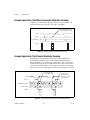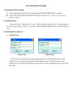
1
DAQ
NI 660x User Manual
NI 6601, NI 6602, and NI 6608 Devices
NI 660x User Manual
December 2006
372119A-01
Support
Worldwide Technical Support and Product Information
ni.com
National Instruments Corporate Headquarters
11500 North Mopac Expressway
Austin, Texas 78759-3504
USA Tel: 512 683 0100
Worldwide Offices
Australia 1800 300 800, Austria 43 0 662 45 79 90 0, Belgium 32 0 2 757 00 20, Brazil 55 11 3262 3599,
Canada 800 433 3488, China 86 21 6555 7838, Czech Republic 420 224 235 774, Denmark 45 45 76 26 00,
Finland 385 0 9 725 725 11, France 33 0 1 48 14 24 24, Germany 49 0 89 741 31 30, India 91 80 41190000,
Israel 972 0 3 6393737, Italy 39 02 413091, Japan 81 3 5472 2970, Korea 82 02 3451 3400,
Lebanon 961 0 1 33 28 28, Malaysia 1800 887710, Mexico 01 800 010 0793, Netherlands 31 0 348 433 466,
New Zealand 0800 553 322, Norway 47 0 66 90 76 60, Poland 48 22 3390150, Portugal 351 210 311 210,
Russia 7 495 783 68 51, Singapore 1800 226 5886, Slovenia 386 3 425 42 00, South Africa 27 0 11 805 8197,
Spain 34 91 640 0085, Sweden 46 0 8 587 895 00, Switzerland 41 56 200 51 51, Taiwan 886 02 2377 2222,
Thailand 662 278 6777, Turkey 90 212 279 3031, United Kingdom 44 0 1635 523545
For further support information, refer to the Technical Support and Professional Services appendix. To comment
on National Instruments documentation, refer to the National Instruments Web site at ni.com/info and enter
the info code feedback.
© 2006 National Instruments Corporation. All rights reserved.
Important Information
Warranty
The NI 6601, NI 6602, and NI 6608 devices are warranted against defects in materials and workmanship for a period of one year from the date
of shipment, as evidenced by receipts or other documentation. National Instruments will, at its option, repair or replace equipment that proves
to be defective during the warranty period. This warranty includes parts and labor.
The media on which you receive National Instruments software are warranted not to fail to execute programming instructions, due to defects in
materials and workmanship, for a period of 90 days from date of shipment, as evidenced by receipts or other documentation. National Instruments
will, at its option, repair or replace software media that do not execute programming instructions if National Instruments receives notice of such defects
during the warranty period. National Instruments does not warrant that the operation of the software shall be uninterrupted or error free.
A Return Material Authorization (RMA) number must be obtained from the factory and clearly marked on the outside of the package before any
equipment will be accepted for warranty work. National Instruments will pay the shipping costs of returning to the owner parts which are covered by
warranty.
National Instruments believes that the information in this document is accurate. The document has been carefully reviewed for technical accuracy. In
the event that technical or typographical errors exist, National Instruments reserves the right to make changes to subsequent editions of this document
without prior notice to holders of this edition. The reader should consult National Instruments if errors are suspected. In no event shall National
Instruments be liable for any damages arising out of or related to this document or the information contained in it.
EXCEPT AS SPECIFIED HEREIN, NATIONAL INSTRUMENTS MAKES NO WARRANTIES, EXPRESS OR IMPLIED, AND SPECIFICALLY DISCLAIMS ANY WARRANTY OF
MERCHANTABILITY OR FITNESS FOR A PARTICULAR PURPOSE. CUSTOMER’S RIGHT TO RECOVER DAMAGES CAUSED BY FAULT OR NEGLIGENCE ON THE PART OF NATIONAL
INSTRUMENTS SHALL BE LIMITED TO THE AMOUNT THERETOFORE PAID BY THE CUSTOMER. NATIONAL INSTRUMENTS WILL NOT BE LIABLE FOR DAMAGES RESULTING
FROM LOSS OF DATA, PROFITS, USE OF PRODUCTS, OR INCIDENTAL OR CONSEQUENTIAL DAMAGES, EVEN IF ADVISED OF THE POSSIBILITY THEREOF. This limitation of
the liability of National Instruments will apply regardless of the form of action, whether in contract or tort, including negligence. Any action against
National Instruments must be brought within one year after the cause of action accrues. National Instruments shall not be liable for any delay in
performance due to causes beyond its reasonable control. The warranty provided herein does not cover damages, defects, malfunctions, or service
failures caused by owner’s failure to follow the National Instruments installation, operation, or maintenance instructions; owner’s modification of the
product; owner’s abuse, misuse, or negligent acts; and power failure or surges, fire, flood, accident, actions of third parties, or other events outside
reasonable control.
Copyright
Under the copyright laws, this publication may not be reproduced or transmitted in any form, electronic or mechanical, including photocopying,
recording, storing in an information retrieval system, or translating, in whole or in part, without the prior written consent of National
Instruments Corporation.
National Instruments respects the intellectual property of others, and we ask our users to do the same. NI software is protected by copyright and other
intellectual property laws. Where NI software may be used to reproduce software or other materials belonging to others, you may use NI software only
to reproduce materials that you may reproduce in accordance with the terms of any applicable license or other legal restriction.
Trademarks
National Instruments, NI, ni.com, and LabVIEW are trademarks of National Instruments Corporation. Refer to the Terms of Use section
on ni.com/legal for more information about National Instruments trademarks.
Other product and company names mentioned herein are trademarks or trade names of their respective companies.
Members of the National Instruments Alliance Partner Program are business entities independent from National Instruments and have no agency,
partnership, or joint-venture relationship with National Instruments.
Patents
For patents covering National Instruments products, refer to the appropriate location: Help»Patents in your software, the patents.txt file
on your CD, or ni.com/patents.
WARNING REGARDING USE OF NATIONAL INSTRUMENTS PRODUCTS
(1) NATIONAL INSTRUMENTS PRODUCTS ARE NOT DESIGNED WITH COMPONENTS AND TESTING FOR A LEVEL OF
RELIABILITY SUITABLE FOR USE IN OR IN CONNECTION WITH SURGICAL IMPLANTS OR AS CRITICAL COMPONENTS IN
ANY LIFE SUPPORT SYSTEMS WHOSE FAILURE TO PERFORM CAN REASONABLY BE EXPECTED TO CAUSE SIGNIFICANT
INJURY TO A HUMAN.
(2) IN ANY APPLICATION, INCLUDING THE ABOVE, RELIABILITY OF OPERATION OF THE SOFTWARE PRODUCTS CAN BE
IMPAIRED BY ADVERSE FACTORS, INCLUDING BUT NOT LIMITED TO FLUCTUATIONS IN ELECTRICAL POWER SUPPLY,
COMPUTER HARDWARE MALFUNCTIONS, COMPUTER OPERATING SYSTEM SOFTWARE FITNESS, FITNESS OF COMPILERS
AND DEVELOPMENT SOFTWARE USED TO DEVELOP AN APPLICATION, INSTALLATION ERRORS, SOFTWARE AND HARDWARE
COMPATIBILITY PROBLEMS, MALFUNCTIONS OR FAILURES OF ELECTRONIC MONITORING OR CONTROL DEVICES,
TRANSIENT FAILURES OF ELECTRONIC SYSTEMS (HARDWARE AND/OR SOFTWARE), UNANTICIPATED USES OR MISUSES, OR
ERRORS ON THE PART OF THE USER OR APPLICATIONS DESIGNER (ADVERSE FACTORS SUCH AS THESE ARE HEREAFTER
COLLECTIVELY TERMED “SYSTEM FAILURES”). ANY APPLICATION WHERE A SYSTEM FAILURE WOULD CREATE A RISK OF
HARM TO PROPERTY OR PERSONS (INCLUDING THE RISK OF BODILY INJURY AND DEATH) SHOULD NOT BE RELIANT SOLELY
UPON ONE FORM OF ELECTRONIC SYSTEM DUE TO THE RISK OF SYSTEM FAILURE. TO AVOID DAMAGE, INJURY, OR DEATH,
THE USER OR APPLICATION DESIGNER MUST TAKE REASONABLY PRUDENT STEPS TO PROTECT AGAINST SYSTEM FAILURES,
INCLUDING BUT NOT LIMITED TO BACK-UP OR SHUT DOWN MECHANISMS. BECAUSE EACH END-USER SYSTEM IS
CUSTOMIZED AND DIFFERS FROM NATIONAL INSTRUMENTS' TESTING PLATFORMS AND BECAUSE A USER OR APPLICATION
DESIGNER MAY USE NATIONAL INSTRUMENTS PRODUCTS IN COMBINATION WITH OTHER PRODUCTS IN A MANNER NOT
EVALUATED OR CONTEMPLATED BY NATIONAL INSTRUMENTS, THE USER OR APPLICATION DESIGNER IS ULTIMATELY
RESPONSIBLE FOR VERIFYING AND VALIDATING THE SUITABILITY OF NATIONAL INSTRUMENTS PRODUCTS WHENEVER
NATIONAL INSTRUMENTS PRODUCTS ARE INCORPORATED IN A SYSTEM OR APPLICATION, INCLUDING, WITHOUT
LIMITATION, THE APPROPRIATE DESIGN, PROCESS AND SAFETY LEVEL OF SUCH SYSTEM OR APPLICATION.
Compliance
Compliance with FCC/Canada Radio Frequency Interference
Regulations
Determining FCC Class
The Federal Communications Commission (FCC) has rules to protect wireless communications from interference. The FCC
places digital electronics into two classes. These classes are known as Class A (for use in industrial-commercial locations only)
or Class B (for use in residential or commercial locations). All National Instruments (NI) products are FCC Class A products.
Depending on where it is operated, this Class A product could be subject to restrictions in the FCC rules. (In Canada, the
Department of Communications (DOC), of Industry Canada, regulates wireless interference in much the same way.) Digital
electronics emit weak signals during normal operation that can affect radio, television, or other wireless products.
All Class A products display a simple warning statement of one paragraph in length regarding interference and undesired
operation. The FCC rules have restrictions regarding the locations where FCC Class A products can be operated.
Consult the FCC Web site at www.fcc.gov for more information.
FCC/DOC Warnings
This equipment generates and uses radio frequency energy and, if not installed and used in strict accordance with the instructions
in this manual and the CE marking Declaration of Conformity*, may cause interference to radio and television reception.
Classification requirements are the same for the Federal Communications Commission (FCC) and the Canadian Department
of Communications (DOC).
Changes or modifications not expressly approved by NI could void the user’s authority to operate the equipment under the
FCC Rules.
Class A
Federal Communications Commission
This equipment has been tested and found to comply with the limits for a Class A digital device, pursuant to part 15 of the FCC
Rules. These limits are designed to provide reasonable protection against harmful interference when the equipment is operated
in a commercial environment. This equipment generates, uses, and can radiate radio frequency energy and, if not installed and
used in accordance with the instruction manual, may cause harmful interference to radio communications. Operation of this
equipment in a residential area is likely to cause harmful interference in which case the user is required to correct the interference
at their own expense.
Canadian Department of Communications
This Class A digital apparatus meets all requirements of the Canadian Interference-Causing Equipment Regulations.
Cet appareil numérique de la classe A respecte toutes les exigences du Règlement sur le matériel brouilleur du Canada.
Compliance with EU Directives
Users in the European Union (EU) should refer to the Declaration of Conformity (DoC) for information* pertaining to the
CE marking. Refer to the Declaration of Conformity (DoC) for this product for any additional regulatory compliance
information. To obtain the DoC for this product, visit ni.com/certification, search by model number or product line,
and click the appropriate link in the Certification column.
* The CE marking Declaration of Conformity contains important supplementary information and instructions for the user or
installer.
Contents
About This Manual
Conventions ...................................................................................................................vii
Related Documentation..................................................................................................viii
Training Courses .............................................................................................viii
Technical Support on the Web ........................................................................ix
Chapter 1
Introduction
About NI 660x Devices..................................................................................................1-1
Using PXI with CompactPCI.........................................................................................1-1
Getting Started ...............................................................................................................1-2
Installing NI-DAQ 7.x .....................................................................................1-2
Installing Other Software ................................................................................1-2
Installing the Hardware ...................................................................................1-2
Accessories and Cables..................................................................................................1-3
Chapter 2
Device Overview
Digital I/O ......................................................................................................................2-1
Prescaling.......................................................................................................................2-1
Pad Synchronization ......................................................................................................2-2
Duplicate Count Prevention...........................................................................................2-4
Example Application That Works Correctly (No Duplicate Counting)..........2-5
Example Application That Works Incorrectly (Duplicate Counting) .............2-6
Example Application That Prevents Duplicate Counting ...............................2-6
Enabling Duplicate Count Prevention in NI-DAQmx.....................................2-7
When to Use Duplicate Count Prevention.......................................................2-7
When Not to Use Duplicate Count Prevention................................................2-7
Transfer Rates ................................................................................................................2-8
High Precision Clock (NI 6608) ....................................................................................2-9
Using the OCXO as the SOURCE Counter ....................................................2-9
Using the OCXO as the 10 MHz PXI Backplane Clock .................................2-9
Measuring OCXO Stable Frequency Deviation ..............................................2-10
Calibration .....................................................................................................................2-12
Register-Level Programming Information.....................................................................2-12
© National Instruments Corporation
v
NI 660x User Manual
Contents
Chapter 3
Signal Connections
Programmable Function Interfaces (PFIs)..................................................................... 3-1
Digital Filtering ............................................................................................................. 3-1
Power-On State.............................................................................................................. 3-3
Pin Assignments ............................................................................................................ 3-4
I/O Connector Pinout..................................................................................................... 3-6
Outputs .......................................................................................................................... 3-8
Counters......................................................................................................................... 3-10
Counter n Source Signal ................................................................................. 3-10
Counter Source to Counter Out Delay.............................................. 3-12
Counter n Gate Signal ..................................................................................... 3-13
Counter n Auxiliary Signal ............................................................................. 3-14
Counter n Internal Output Signal .................................................................... 3-14
Hardware Arm Start Triggers ......................................................................... 3-15
Counter Pairs................................................................................................... 3-15
Counter Applications ...................................................................................... 3-15
Real-Time System Integration Bus ............................................................................... 3-16
RTSI Triggers ................................................................................................. 3-16
+5 V Power Source........................................................................................................ 3-18
I/O Signals ..................................................................................................................... 3-19
Field Wiring Considerations ........................................................................... 3-19
Noise ............................................................................................................... 3-19
Crosstalk.......................................................................................................... 3-20
Inductive Effects ............................................................................................. 3-21
Transmission Line Effects .............................................................................. 3-23
Appendix A
Technical Support and Professional Services
Glossary
Index
NI 660x User Manual
vi
ni.com
About This Manual
This manual describes the electrical and mechanical aspects of the National
Instruments NI 6601, NI 6602, and NI 6608 devices, and contains
information about device operation and programming. Unless otherwise
noted, text applies to all NI 660x devices. The PCI and PXI
implementations are the same in functionality; their primary difference
is the bus interface.
Conventions
The following conventions are used in this manual:
<>
Angle brackets that contain numbers separated by an ellipsis represent
a range of values associated with a bit or signal name—for example,
AO <3..0>.
»
The » symbol leads you through nested menu items and dialog box options
to a final action. The sequence File»Page Setup»Options directs you to
pull down the File menu, select the Page Setup item, and select Options
from the last dialog box.
This icon denotes a note, which alerts you to important information.
This icon denotes a caution, which advises you of precautions to take to
avoid injury, data loss, or a system crash. When this symbol is marked on a
product, refer to the Read Me First: Safety and Radio-Frequency
Interference document for information about precautions to take.
bold
Bold text denotes items that you must select or click in the software, such
as menu items and dialog box options. Bold text also denotes parameter
names.
italic
Italic text denotes variables, emphasis, a cross-reference, or an introduction
to a key concept. Italic text also denotes text that is a placeholder for a word
or value that you must supply.
monospace
Text in this font denotes text or characters that you should enter from the
keyboard, sections of code, programming examples, and syntax examples.
This font is also used for the proper names of disk drives, paths, directories,
programs, subprograms, subroutines, device names, functions, operations,
variables, filenames, and extensions.
© National Instruments Corporation
vii
NI 660x User Manual
About This Manual
Related Documentation
The following documents contain information that you might find helpful
as you use this help file:
Note
•
NI 660x Specifications—This document contains specifications for the
NI 6601, NI 6602, and NI 6608 devices. It available for download at
ni.com/manuals.
•
DAQ Getting Started Guide—This guide describes how to install the
NI-DAQ 7.x software and the DAQ device, and how to confirm that the
device is operating properly.
•
NI-DAQmx Help—This help file contains information about using
NI-DAQmx to program National Instruments devices. NI-DAQmx is
the software you use to communicate with and control your DAQ
device.
•
Measurement & Automation Explorer Help for NI-DAQmx—This help
file contains information about configuring and testing DAQ devices,
SCXI devices, SCC devices, and RTSI cables using Measurement &
Automation Explorer (MAX) for NI-DAQmx, and information about
special considerations for operating systems.
•
DAQ Assistant Help—This help file contains information about
creating and configuring channels, tasks, and scales using the DAQ
Assistant.
•
PXI Hardware Specification Revision 2.1—This document introduces
the PXI architecture and describes the electrical, mechanical, and
software requirements for PXI.
You can download these documents at ni.com/manuals.
Training Courses
If you need more help getting started developing an application with NI
products, NI offers training courses. To enroll in a course or obtain a
detailed course outline, refer to ni.com/training.
NI 660x User Manual
viii
ni.com
About This Manual
Technical Support on the Web
For additional support, refer to ni.com/support or zone.ni.com.
Note
You can download these documents at ni.com/manuals.
DAQ specifications and some DAQ manuals are available as PDFs. You
must have Adobe Acrobat Reader with Search and Accessibility 5.0.5 or
later installed to view the PDFs. Refer to the Adobe Systems Incorporated
Web site at www.adobe.com to download Acrobat Reader. Refer to the
National Instruments Product Manuals Library at ni.com/manuals for
updated documentation resources.
© National Instruments Corporation
ix
NI 660x User Manual
1
Introduction
This chapter describes the NI 660x devices, lists what you need to get
started, and describes optional equipment. If you have not already installed
the TIO device, refer to the DAQ Getting Started Guide.
About NI 660x Devices
The NI 660x devices are timing and digital I/O devices for use with the
PCI bus in PC-compatible computers, or PXI or CompactPCI chassis.
The NI 6601 offers four 32-bit counter channels and up to 32 lines of
individually configurable, TTL/CMOS-compatible digital I/O. The
NI 6602 offers this capability and four additional 32-bit counter channels.
The NI 6608 is a functional superset of the NI 6602 device with a
high-stability clock called an oven-controlled crystal oscillator (OCXO).
The counter/timer channels have many measurement and generation
modes, such as event counting, time measurement, frequency
measurement, encoder position measurement, pulse generation, and
square-wave generation.
The NI 660x devices contain the National Instruments MITE PCI interface.
The MITE offers bus-master operation, PCI burst transfers, and high-speed
DMA controller(s) for continuous, scatter-gather DMA without requiring
DMA resources from your computer. Refer to the Using PXI with
CompactPCI section for more information about your NI PXI-660x device.
Device specifications are available in the NI 660x Specifications document,
which is available for download from ni.com/manuals.
Using PXI with CompactPCI
Using PXI-compatible products with standard products is an important
feature provided by PXI Hardware Specification Revision 2.1. If you use a
PXI-compatible plug-in module in a standard chassis, you cannot use
PXI-specific functions, but you can still use the basic plug-in device
functions. For example, the RTSI bus on a PXI TIO Series device is
available in a PXI chassis, but not in a CompactPCI chassis.
© National Instruments Corporation
1-1
NI 660x User Manual
Chapter 1
Introduction
The specification permits vendors to develop sub-buses that coexist with
the basic PCI interface on the bus. Compatible operation is not guaranteed
between devices with different sub-buses nor between devices with
sub-buses and PXI. The standard implementation for does not include
these sub-buses. The PXI TIO Series device works in any standard chassis
adhering to the PICMG 2.0 R3.0 core specification.
PXI-specific features are implemented on the J2 connector of the bus. The
PXI device is compatible with any chassis with a sub-bus that does not
drive the lines used by that device. Even if the sub-bus is capable of driving
these lines, the PXI device is still compatible as long as those pins on the
sub-bus are disabled by default and never enabled.
Caution Damage can result if these lines are driven by the sub-bus. NI is not liable for any
damage resulting from improper signal connections.
Getting Started
Before installing your DAQ device, you must install the software you plan
to use with the device.
Installing NI-DAQ 7.x
If you are using NI-DAQ 7.1 or later, refer to the DAQ Getting
Started Guide, which you can download at ni.com/manuals.
The DAQ Getting Started Guide offers NI-DAQ users step-by-step
instructions for installing software and hardware, configuring channels
and tasks, and getting started developing an application.
Installing Other Software
If you are using other software, refer to the installation instructions that
accompany your software.
Installing the Hardware
The DAQ Getting Started Guide contains non-software-specific
information about how to install PCI, PXI, PCMCIA, and USB/IEEE 1394
devices, as well as accessories and cables.
NI 660x User Manual
1-2
ni.com
Chapter 1
Introduction
Accessories and Cables
Table 1-1 lists the accessories and cables available for use with
NI 660x devices.
Table 1-1. Accessories and Cables
Accessory
© National Instruments Corporation
Description
SH68-68-D1
Shielded 68-conductor cable
R6868 cable
68-conductor flat ribbon cable
BNC-2121
BNC connector block with built-in test features
CA-1000
Configurable connector accessory
SCB-68
Shielded screw connector block
TB-2715
Front-mount terminal block for NI PXI-660x
TBX-68
DIN-rail connector block
CB-68LP
Low-cost screw connector block
CB-68LPR
Low-cost screw connector block
1-3
NI 660x User Manual
2
Device Overview
This chapter provides information about NI 660x device functionality.
Digital I/O
The NI 660x devices have a 32-bit DIO port on PFI <0..31>. Digital I/O
consists of asynchronous reads and writes to the digital port upon software
command. You can individually configure each line for digital input or
output. For output, you can individually configure PFI <8..31> for either
counter-associated output or digital output. You must specify whether you
are using the PFI line for counter I/O or digital I/O only if that line is being
used as an output. For input, both counter I/O and digital I/O can share the
lines on PFI <0..31>.
For more information about the signals that can be driven onto PFI lines,
refer to the I/O Connector Pinout section of this document.
For information about how to implement specific digital I/O functions,
refer to the application software documentation.
Prescaling
Prescaling allows the counter to count a signal that is faster than the
maximum timebase of the counter. The counters on the NI 660x offer
8X and 2X prescaling on each counter (prescaling can be disabled).
Each prescaler consists of a small, simple counter that counts to eight
(or two) and rolls over. This counter is specifically designed for this
application and can count signals that are faster than the general purpose
counters. The CtrnSource signal on the general purpose counter will be the
divided signal from the simple counter.
© National Instruments Corporation
2-1
NI 660x User Manual
Chapter 2
Device Overview
Figure 2-1 shows an example of prescaling.
External Signal
Prescaler Rollover
(Used as Source
by Counter)
Counter Value
0
1
Figure 2-1. Prescaling Example
Prescaling is intended for use with two counter period and frequency
measurements where the measurement is made on a continuous, repetitive
signal. The prescaling counter cannot be read, so you cannot determine how
many edges have occurred since the previous roll-over. You can also use
prescaling for counting edges if it is acceptable to have an error of up to
seven when using 8X prescaling or one when using 2X prescaling.
Pad Synchronization
The NI 660x devices allow synchronization of their PFI lines and RTSI
lines at the I/O pads. This is called pad synchronization in this document,
and digital synchronization in the NI-DAQmx API. You cannot use digital
filtering while enabling this feature.
Pad synchronization is useful when several counters are measuring or
operating off the same external signal. For example, suppose
counters 0 and 1 are configured for triggered pulse generation and each
counter uses the same external trigger (this external signal is connected to
PFI 38 on the I/O connector and both counters have PFI 38 selected as their
GATE). After the trigger signal propagates through the I/O pad of the
ASIC, the time for the signal to reach the GATE of each counter within the
ASIC may differ by a few nanoseconds.
This signal is sampled at the counters’ GATEs using the selected SOURCE.
Because of different propagation times for the paths to the two GATEs,
it is possible for the counters to detect the trigger on different edges on
SOURCE. Thus, one counter could see the trigger one SOURCE period
after the other. If you want to allow the counters to see the changes in the
signal at the same instance, you should use pad synchronization. During
pad synchronization, the signal is offset by one clock cycle.
This feature is useful in applications with two or more counters that are
armed by an external start trigger, or that use the same PFI line as a counter
control signal. Pad synchronization is only useful if the counters involved
NI 660x User Manual
2-2
ni.com
Chapter 2
Device Overview
are using one of the internal timebases. A counter is using maximum
timebase as its source if the synchronous counting mode is enabled for
that counter.
Figures 2-2 and 2-3 illustrate how pad synchronization can be useful.
These figures assume a 1.5 and a 1.75 SOURCE cycle delay between the
PFI 38 input pin, and CTR 0 GATE and CTR 1 GATE, respectively. These
delay values are exaggerated and are used for illustrative purposes.
Figure 2-2 shows counter 0 at the gate edge on PFI 38 one source period
before counter 1. Figure 2-3 shows both counters at the gate edge on PFI 38
at the same time.
Counter
Source
PFI 38
at Input To ASIC
1 1/2 Cycles
PFI 38
at CTR 0 GATE
PFI 38
at CTR 1 GATE
1/4 Cycle
Synchronized
GATE at Ctr0
Synchronized
GATE at Ctr1
Figure 2-2. Counter 0 at Gate Edge on PFI 38 One Source Period before Counter 1
© National Instruments Corporation
2-3
NI 660x User Manual
Chapter 2
Device Overview
Counter
Source
PFI 38
at Input to ASIC
PFI 38
Synchronized at Pad
PFI 38
at CTR 0 GATE
1 1/2
Cycles
PFI 38
at CTR 1 GATE
1/4 Cycle
Synchronized
GATE at Ctr0
Synchronized
GATE at Ctr1
Figure 2-3. Counters 0 and 1 at Gate Edge on PFI 38 at the Same Time
Duplicate Count Prevention
Duplicate count prevention (or synchronous counting mode) ensures that a
counter returns correct data in applications that are a slow or non-periodic
external source. Duplicate count prevention applies only to buffered
counter applications such as measuring frequency or period.
For such buffered applications, the counter should store the number of
times an external source pulses between rising edges on the Gate signal.
NI 660x User Manual
2-4
ni.com
Chapter 2
Device Overview
Example Application That Works Correctly (No Duplicate Counting)
Figure 2-4 shows an external buffered signal as the period measurement
Source.
Rising Edge
of Gate
Counter detects rising edge
of Gate on the next rising
edge of Source.
Gate
Source
Counter Value
6
7
1
7
Buffer
2
1
2
7
Figure 2-4. Example Application That Works Correctly
On the first rising edge of the Gate, the current count of 7 is stored. On the
next rising edge of the Gate, the counter stores a 2 because two Source
pulses occurred after the previous rising edge of Gate.
The counter synchronizes or samples the Gate signal with the Source
signal. So the counter does not detect a rising edge in the Gate until the next
Source pulse. In this example, the counter stores the values in the buffer on
the first rising Source edge after the rising edge of Gate.
© National Instruments Corporation
2-5
NI 660x User Manual
Chapter 2
Device Overview
Example Application That Works Incorrectly (Duplicate Counting)
In Figure 2-5, after the first rising edge of Gate, no Source pulses occur.
So the counter does not write the correct data to the buffer.
No Source edge, so no
value written to buffer.
Gate
Source
Counter Value
6
7
1
7
Buffer
Figure 2-5. Example Application That Works Incorrectly
Example Application That Prevents Duplicate Counting
With duplicate count prevention enabled, the counter synchronizes
both the Source and Gate signals to the maximum onboard timebase.
By synchronizing to the timebase, the counter detects edges on the Gate
even if the Source does not pulse. This enables the correct current count to
be stored in the buffer even if no Source edges occur between Gate signals.
Figure 2-6 shows an example application that prevents duplicate counting.
Counter detects
rising Gate edge.
Counter value
increments only
one time for each
Source pulse.
Gate
Source
80 MHz Timebase
Counter Value
Buffer
6
7
0
1
7
0
7
Figure 2-6. Example Application That Prevents Duplicate Counting
NI 660x User Manual
2-6
ni.com
Chapter 2
Device Overview
Even if the Source pulses are long, the counter increments only once for
each source pulse.
Normally, the counter and Counter n Internal Output signals change
synchronously to the Source signal. With duplicate count prevention, the
counter value and Counter n Internal Output signals change synchronously
to the maximum onboard timebase.
Notice that duplicate count prevention should only be used if the frequency
of the Source signal is one-fourth of the maximum onboard timebase.
Enabling Duplicate Count Prevention in NI-DAQmx
You can enable duplicate count prevention in NI-DAQmx by setting the
Enable Duplicate Count Prevention attribute/property. For specific
information on finding the Enable Duplicate Count Prevention
attribute/property, refer to the help file for the API you are using. Refer to
the NI-DAQmx Help for more information.
When to Use Duplicate Count Prevention
Use duplicate count prevention for buffered measurements that use an
external CtrnSource signal and the frequency of the signal is less than or
equal to one-fourth of the maximum onboard timebase. Use this mode if
you are using a low frequency or you expect zero CtrnSource edges
between successive edges of the CtrnGate signal.
You should use duplicate count prevention if the following conditions are
true:
•
You are making a buffered counter input measurement
•
You are using an external signal (such as PFI x) as the counter Source
•
The frequency of the external source is one-fourth of the maximum
onboard timebase
•
You can have the counter value and output to change synchronously
with the maximum onboard timebase
In all other cases, you should not enable duplicate count prevention.
When Not to Use Duplicate Count Prevention
Use duplicate counter prevention only for buffered measurements with an
external CtrnSource signal. Do not use it when the CtrnSource signal is
greater than one-fourth of the maximum timebase.
© National Instruments Corporation
2-7
NI 660x User Manual
Chapter 2
Device Overview
Transfer Rates
The maximum sustainable transfer rate a TIO device can achieve for a
buffered acquisition depends on the following factors:
•
Amount of available bus bandwidth
•
Processor speed and operating system
•
Application software
To reduce the amount of bus activity, limit the number of devices
generating bus cycles. Because direct-memory access (DMA) transfers are
faster than interrupt-driven transfers, NI-DAQmx uses DMA by default for
buffered acquisitions.
Note
The maximum sustainable transfer rate is always lower than the peak transfer rate.
Table 2-1 lists the maximum transfer rates for TIO devices.
Table 2-1. Maximum Transfer Rates
DMA
Interrupt
Finite Operation
Buffer Size (Samples)
Rate (kS/s)
Buffer Size (Samples)
Rate (kS/s)
100
5,000
100
77
1,000
2,150
1,000
77
10,000
1,600
10,000
77
100,000
1,350
100,000
77
Continuous Operation
Buffer Size (Samples)
Rate (kS/s)
Buffer Size (Samples)
Rate (kS/s)
100
44
100
7
1,000
202
1,000
46
10,000
212
10,000
75
100,000
245
100,000
76
default
212
default
75
NI 660x User Manual
2-8
ni.com
Chapter 2
Device Overview
Note Transfer rates may vary depending on your computer hardware, operating system
and system activity. This benchmark data was determined on an AMD Athlon XP 1800
computer with 128 MB of PC-2100 DDR RAM running Windows XP and LabVIEW using
one counter of the TIO device. For continuous measurements, the transfer rate is the
maximum sustained rate for 30 seconds on one counter.
High Precision Clock (NI 6608)
The accuracy of your time measurement and pulse generation is determined
by the timing accuracy of your counter clock. The NI 6608 device has an
oven-controlled crystal oscillator (OCXO) that provides a highly stable
10 MHz clock that you can use as a GATE or SOURCE of a counter. You
can also use the OCXO as the PXI backplane clock. Modules phase locked
to the PXI backplane clock will acquire the same clock stability as the
NI 6608. For more information, refer to the KnowledgeBase at
ni.com/support and search using keyword phase lock.
Using the OCXO as the SOURCE Counter
Using the OCXO as the timebase source of the counter, you can route the
10 MHz clock to CtrnSource.
Using the OCXO as the 10 MHz PXI Backplane Clock
Your PXI chassis has a built-in 10 MHz backplane clock that is
independently routed to each peripheral slot. An independent buffer on the
chassis drives the clock signal to each peripheral slot with a skew of less
than 1 ns between slots. You can use this common reference clock signal to
synchronize multiple modules in a measurement or control system.
Use the OCXO 10 MHz clock to drive the PXI backplane clock so the
modules in the other slots can take advantage of the stable timebase.
On NI PXI-660x devices, the maximum timebase is phase locked to the PXI
backplane clock.
Note
To use the OCXO 10 MHz clock as the PXI backplane clock, plug the
NI PXI-6608 device into the Star Trigger Controller Slot, Slot 2, or the slot
immediately to the right of the controller of the PXI chassis.
By default, NI-DAQ software drives the 10 MHz clock from the OCXO
onto the PXI star trigger so that it is used as the PXI backplane clock. When
the PXI chassis senses a clock on PXI star trigger in Slot 2, the chassis
© National Instruments Corporation
2-9
NI 660x User Manual
Chapter 2
Device Overview
disables its internal clock, then uses the OCXO clock instead, illustrated in
Figure 2-7.
PXI Backplane
NI PXI-6608 in Slot 2
of PXI Chassis
10 MHz
TIO(0)
(Driving
10 MHz
Supplied by
OCXO)
10 MHz
OCXO
TIO(1)
80 MHz Phase Locked to
10 MHz PXI Backplane Clock
Phase
Lock
Loop
10 MHz PXI Backplane Clock
NI PXI-6608 or NI PXI-6602
in Slot 3 of PXI Chassis
TIO(0)
Phase
Lock
Loop
PXI Star
(Not Used
for
Backplane
Clock)
10 MHz
OCXO
80 MHz
VCXO
Circuit
to
Drive
10 MHz
PXI
Backplane
Clock
TIO(1)
80 MHz Phase Locked to
10 MHz PXI Backplane Clock
10 MHz from OCXO is Used as
10 MHz PXI Backplane Clock
80 MHz
VCXO
PXI CLK10 in
10 MHz PXI Backplane Clock
Figure 2-7. OCXO as the 10 MHz PXI Backplane Clock
Measuring OCXO Stable Frequency Deviation
When you power the NI 6608 device, the OCXO requires adequate
warm-up time to reach stable frequency. Five minutes is adequate warm-up
time for a power-off duration of less than one hour, with maximum
deviation within 20 ppb, or parts per billion, while four hours of operation
is adequate for a power-off duration of up to 90 days.
NI 660x User Manual
2-10
ni.com
Chapter 2
Note
Device Overview
For best performance, minimize power-off periods for the OCXO.
The OCXO is calibrated to within 0.1 Hz of 10.000000 MHz prior to
shipment. Table 2-2 shows additional change in stable frequency that
occurs over time. A change in stable frequency of approximately 45 ppb
occurs after the first year of normal use.
Table 2-2. Change in Stable Frequency over Time
Days of Operation
Additional Change in
Stable Frequency (ppb)
0–10
11.25
11–60
11.25
61–200
11.25
201–365
11.25
366–375
5.63
376–425
5.63
426–565
5.63
566–730
5.63
731–740
2.82
741–790
2.82
For example, if the OCXO has a perfect stable frequency of 10 MHz after
warm-up, after the first 10 days of operation, the stable frequency drifts
11.25 ppb. During the next 50 days of operation, this frequency will drift
an additional 11.25 ppb, thus making the total drift caused by aging to be
22.5 ppb. After 365 days, drift will be 45 ppb. If you calibrate the OCXO
after 365 days of operation to restore the stable frequency to a perfect
10 MHz, the drift during the first 10 days following calibration
(days 366–375) will now be 5.63 ppb—the stable frequency in this case
will be 10 MHz ± 5.63 ppb after 375 days of operation. Calibration does
not affect the drift in frequency; it only changes the stable frequency.
© National Instruments Corporation
2-11
NI 660x User Manual
Chapter 2
Device Overview
Calibration
When you are ready to calibrate your device to correct for drift in
frequency, refer to the 6601/6602 Calibration Procedure or the
6608 Calibration Procedure available at ni.com/calibration. Click
on Manual Calibration Procedures and select your device from the list.
You can calibrate these devices in Traditional NI-DAQ (Legacy) only.
When calibrating the NI 6608, use an external clock with a short-term stability (over
a period of 100 s) of better than 5 × 10–11; otherwise, the OCXO will be improperly
calibrated. A typical rubidium time standard will meet the required stability.
Note
Register-Level Programming Information
Caution NI is not liable for any damage or injury that results from register-level
programming the TIO Series devices.
For information about programming the NI 660x devices at the register
level, refer to the NI 660X Register-Level Programmer Manual, available
from ni.com/manuals.
The National Instruments Measurement Hardware DDK provides
development tools and a register-level programming interface for NI data
acquisition hardware. The NI Measurement Hardware DDK provides
access to the full register map of each device and offers examples for
completing common measurement and control functions. The
Measurement Hardware DDK works with TIO Series digital I/O and
counter/timer I/O devices. Refer to ni.com for more information.
NI 660x User Manual
2-12
ni.com
3
Signal Connections
This chapter describes how to make input and output signal connections to
the NI 660x device by way of the device I/O connector and the RTSI
connector.
Programmable Function Interfaces (PFIs)
The 40 PFI pins are connected to the signal routing multiplexer for each
timing signal, and software can select a PFI as the external source for a
given timing signal. Any PFI pin can be used as an input by any timing
signal and multiple timing signals can simultaneously use the same PFI pin.
This flexible routing scheme reduces the need to change physical
connections to the I/O connector for different applications. You also can
individually enable each PFI pin to output a specific internal timing signal.
You can individually enable many of the PFI pins to output a specific
internal timing signal. For example, if you need the Counter 0 Source signal
as an output on the I/O connector, software can turn on the output driver for
the PFI 39/CTR 0 SRC pin.
Caution
Do not drive a PFI signal externally when it is configured as an output.
When using the PFI pin as an input, you can individually configure each
PFI for edge or level detection and for polarity selection. You can use the
polarity selection for any of the timing signals, but the edge or level
detection depends upon the particular timing signal being controlled.
The detection requirements for each timing signal are listed within the
section that discusses that signal.
Digital Filtering
Each PFI line coming from the I/O connector can be passed through a
simple digital debouncing filter. The filter operates off a filter clock and a
fast internal sampling clock. The filter circuit samples the signal on the PFI
line on each rising edge of the sampling clock. A change in the signal is
propagated only if it maintains its new state for at least the duration
© National Instruments Corporation
3-1
NI 660x User Manual
Chapter 3
Signal Connections
between two consecutive rising edges of the filter clock timebase. The
frequency of the filter clock timebase determines whether a transition in the
signal may propagate or not. The function of the internal sampling clock is
to increase the sampling rate and prevent aliasing. Figure 3-1 demonstrates
the function of this filter.
External Signal
on PFI Line
Filter Clock
Maximum Timebase
External Signal Sample
by Maximum Timebase
H L L H H
H H H H H
Filtered PFI Line
Figure 3-1. Digital Filtering
In Figure 3-1, the low-to-high transition is guaranteed to be passed through
only if the signal remains high for at least two periods of the filter clock
timebase and is sampled high at each sampling clock rising edge during this
time. Although the low-to-high transition is shown in this example, the
same is true for high-to-low transitions.
The effect of filtering is that the signal transition is shifted by two filter clock
timebase periods.
Note
Figure 3-1 shows that if sampling was done at each rising edge of the filter
clock timebase alone, the first two pulses would have been seen as one
continuous transition. However, using the faster sampling clock detects the
glitch; thus, the two short pulses are ignored.
The intent of the filter is to eliminate glitches that may appear on a signal.
The filter is sensitive to the duration for which a digital signal transitions
from one state to another. If a square wave is applied to the filter, its
propagation will depend on its frequency and duty cycle.
There are four filter settings available in the TIO devices: 5 μs, 1 μs, 500 ns,
and 100 ns. The 5 μs filter will pass all pulse widths (high and low) that are
5 μs or longer. It will block all pulse widths that are 2.5 μs (one-half of
5 μs) or shorter. Pulse widths between 2.5 μs and 5 μs may or may not pass,
depending on the phase of the pulse with respect to the filter clock
timebase. The same relationship extends to all other filter clocks.
NI 660x User Manual
3-2
ni.com
Chapter 3
Signal Connections
In addition to these hard-wired filter clocks, you can use any PFI, RTSI, or
internal signal as the source for the filter clock timebase. Use signals with
a duty cycle as close to 50 percent as possible.
If the period of the filter clock timebase is tfltrclk, this filter guarantees to
pass pulse widths that are 2*tfltrclk or longer and to block pulse widths that
are tfltrclk or shorter. A pulse with a width between these two ranges may or
may not pass, depending on the phase of the pulse with respect to the filter
clock timebase.
Table 3-1 summarizes the properties of the different filter settings.
Table 3-1. Filter Settings
Filter Setting
Pulse Width Passed
Pulse Width Blocked
5 μs
5 μs
2.5 μs
1 μs
1 μs
500 ns
500 ns
500 ns
250 ns
100 ns
100 ns
50 ns
Programmable setting
with period of clock = tfltrclk
2*tfltrclk
tfltrclk
You individually configure the filter setting for each PFI line. The filters are
useful to maintain signal integrity. They can prevent measurement errors
caused by noise, crosstalk, or transmission line effects.
Note
The digital filters on the NI 660x devices are not enabled by default.
For more information about using the digital filters on your device, refer to
Digital Filtering for Counters in the NI-DAQmx Help.
Power-On State
The PFI lines are weakly pulled down within the NI-TIO ASIC, and the
RTSI lines are weakly pulled high. Connections for pulling up the PFI lines
or for stronger pull-down connections must be made external to the
NI 660x. These connections affect the drive strength of the NI 660x when
the lines pulled up or down are used as outputs.
© National Instruments Corporation
3-3
NI 660x User Manual
Chapter 3
Signal Connections
Pin Assignments
Table 3-2 lists the pin assignments for the I/O connector on the NI 660x.
Note
The NI 6601 uses counters <0..3> only.
Table 3-2. NI 660x Connector Pin Assignments
Signal
Name
PFI 31
Motion
Encoder
Context
channel
A(2)
DIO
Context
Counter
Context
(Default)
Pin
Number
Pin
Number
Counter
Context
(Default)
DIO
Context
Motion
Encoder
Context
—
D GND
P0.31
CTR 2
SRC
34
68
—
—
Signal
Name
D GND
—
—
—
33
67
CTR 2
GATE
P0.30
index/z(2)
PFI 30
PFI 28
—
P0.28
CTR 2
OUT
32
66
CTR 2
AUX
P0.29
channel
B(2)
PFI 29
P0.27
CTR 3
SRC
31
65
—
—
PFI 27
channel
A(3)
—
D GND
D GND
—
—
—
30
64
CTR 3
GATE
P0.26
index/z(3)
PFI 26
PFI 24
—
P0.24
CTR 3
OUT
29
63
CTR 3
AUX
P0.25
channel
B(3)
PFI 25
P0.23
CTR 4
SRC
28
62
—
—
PFI 23
channel
A(4)
—
D GND
D GND
—
—
—
27
61
CTR 4
GATE
P0.22
index/z(4)
PFI 22
PFI 20
—
P0.20
CTR 4
OUT
26
60
CTR 4
AUX
P0.21
channel
B(4)
PFI 21
P0.19
CTR 5
SRC
25
59
—
—
PFI 19
channel
A(5)
—
D GND
D GND
—
—
—
24
58
CTR 5
GATE
P0.18
index/z(5)
PFI 18
PFI 16
—
P0.16
CTR 5
OUT
23
57
CTR 5
AUX
P0.17
channel
B(5)
PFI 17
PFI 15
channel
A(6)
P0.15
CTR 6
SRC
22
56
—
—
—
RG
PFI 14
index/z(6)
P0.14
CTR 6
GATE
21
55
—
—
—
D GND
NI 660x User Manual
3-4
ni.com
Chapter 3
Signal Connections
Table 3-2. NI 660x Connector Pin Assignments (Continued)
Motion
Encoder
Context
DIO
Context
Counter
Context
(Default)
D GND
—
—
RG
—
D GND
—
Signal
Name
PFI 9
channel
B(7)
Counter
Context
(Default)
DIO
Context
Motion
Encoder
Context
Pin
Number
Pin
Number
—
20
54
CTR 6
AUX
P0.13
—
—
19
53
CTR 6
OUT
P0.12
—
—
18
52
CTR 7
SRC
P0.11
channel
A(7)
PFI 11
P0.9
CTR 7
AUX
17
51
CTR 7
GATE
P0.10
index/z(7)
PFI 10
channel
B(6)
—
Signal
Name
PFI 13
PFI 12
PFI 8
—
P0.8
CTR 7
OUT
16
50
—
—
—
D GND
PFI 7
—
P0.7
—
15
49
—
—
—
D GND
D GND
—
—
14
48
—
P0.6
—
PFI 6
PFI 4
—
P0.4
—
13
47
—
P0.5
—
PFI 5
PFI 3
—
P0.3
—
12
46
—
—
D GND
D GND
—
—
11
45
—
P0.2
—
PFI 2
PFI 0
—
—
10
44
—
P0.1
—
PFI 1
PFI 32
—
—
CTR 1
OUT
9
43
—
—
—
RG
PFI 34
index/z(1)
—
CTR 1
GATE
8
42
—
—
—
D GND
PFI 35
channel
A(1)
—
CTR 1
SRC
7
41
—
—
—
D GND
PFI 33
channel
B(1)
—
CTR 1
AUX
6
40
CTR 0
AUX
—
—
—
P0.0
—
channel
B(0)
PFI 37
PFI 36
—
—
CTR 0
OUT
5
39
—
—
—
D GND
Reserved
—
—
—
4
38
—
—
—
Reserved
PFI 38
index/z(0)
—
CTR 0
GATE
3
37
—
—
—
Reserved
PFI 39
channel
A(0)
—
CTR 0
SRC
2
36
—
—
—
GND
—
—
1
35
—
—
—
RG
+5 V
—
© National Instruments Corporation
3-5
NI 660x User Manual
Chapter 3
Signal Connections
I/O Connector Pinout
Figure 3-2 shows the pin assignments for the I/O connectors on the
NI 660x.
Note
NI 660x User Manual
The NI 6601 uses counters <0..3> only.
3-6
ni.com
Chapter 3
PFI 31/P0.31/CTR 2 SOURCE
D GND
PFI 28/P0.28/CTR 2 OUT
PFI 27/P0.27/CTR 3 SOURCE
D GND
PFI 24/P0.24/CTR 3 OUT
PFI 23/P0.23/CTR 4 SOURCE1
D GND
CTR 4 OUT/PFI 20/P0.201
PFI 19/P0.19/CTR 5 SOURCE1
D GND
CTR 5 OUT/PFI 16/P0.161
PFI 15/P0.15/CTR 6 SOURCE1
PFI 14/P0.14/CTR 6 GATE1
D GND
R GND
D GND
PFI 9/P0.9/CTR 7 AUX1
CTR 7 OUT/PFI 8/P0.81
PFI 7/P0.7
D GND
PFI 4/P0.4
PFI 3/P0.3
D GND
PFI 0/P0.0
PFI 32/CTR 1 OUT
PFI 34/CTR 1 GATE
PFI 35/CTR 1 SOURCE
PFI 33/CTR 1 AUX
PFI 36/CTR 0 OUT
RESERVED
PFI 38/CTR 0 GATE
PFI 39/CTR 0 SOURCE
+5 V
34
33
32
31
30
29
28
27
26
25
24
23
68
67
66
65
64
63
62
61
60
59
58
57
22
21
20
19
18
17
16
56
55
54
53
52
51
50
15
14
13
12
11
10
9
8
7
6
5
4
3
2
1
49
48
47
46
45
44
43
42
41
40
39
38
37
36
35
Signal Connections
D GND
PFI 30/P0.30/CTR 2 GATE
PFI 29/P0.29/CTR 2 AUX
D GND
PFI 26/P0.26/CTR 3 GATE
PFI 25/P0.25/CTR 3 AUX
D GND
PFI 22/P0.22/CTR 4 GATE1
PFI 21/P0.21/CTR 4 AUX1
D GND
PFI 18/P0.18/CTR 5 GATE1
PFI 17/P0.17/CTR 5 AUX1
R GND
D GND
PFI 13/P0.13/CTR 6 AUX1
CTR 6 OUT/PFI 12/P0.121
PFI 11/P0.11/CTR 7 SOURCE1
PFI 10/P0.10/CTR 7 GATE1
D GND
D GND
PFI 6/P0.6
PFI 5/P0.5
D GND
PFI 2/P0.2
PFI 1/P0.1
R GND
D GND
D GND
PFI 37/CTR 0 AUX
D GND
RESERVED
RESERVED
D GND
R GND
RG: Reserved if using an SH68-68-D1 shielded
cable. Ground if using an R6868 ribbon cable.
1 No Connect on NI 6601
Figure 3-2. NI 660x Connector Pinout
© National Instruments Corporation
3-7
NI 660x User Manual
Chapter 3
Signal Connections
Outputs
PFI <0..7> are used for DIO only. PFI <32..39> are used for counters and
motion encoders only. You can use PFI <8..31> as either of the three
choices. When used as an output, you can individually configure each PFI
line as a DIO line or a counter line (you need not distinguish between
counter/encoder or DIO applications when you use a PFI line as an input).
Furthermore, the PFI lines associated with gates and sources can be used as
outputs associated with the counter. When used as such, these PFI lines
drive the selected GATE or SOURCE associated with these lines. For
example, if PFI 39 is configured as an output, it will drive the selected
SOURCE of counter 0.
Table 3-3 summarizes what you can drive onto the different PFI lines when
they are used as outputs.
Table 3-3. PFI Lines Used as Outputs
PFI Line
NI 660x User Manual
Possible Signals
PFI 0
P0.0
PFI 1
P0.1
PFI 2
P0.2
PFI 3
P0.3
PFI 4
P0.4
PFI 5
P0.5
PFI 6
P0.6
PFI 7
P0.7
PFI 8
P0.8 or CTR 7 OUT1
PFI 9
P0.9
PFI 10
P0.10 or CTR 7 GATE1
PFI 11
P0.11 or CTR 7 SOURCE1
PFI 12
P0.12 or CTR 6 OUT1
PFI 13
P0.13
PFI 14
P0.14 or CTR 6 GATE1
3-8
ni.com
Chapter 3
Signal Connections
Table 3-3. PFI Lines Used as Outputs (Continued)
PFI Line
PFI 15
P0.15 or CTR 6 SOURCE1
PFI 16
P0.16 or CTR 5 OUT
PFI 17
P0.17
PFI 18
P0.18 or CTR 5 GATE1
PFI 19
P0.19 or CTR 5 SOURCE1
PFI 20
P0.20 or CTR 4 OUT1
PFI 21
P0.21
PFI 22
P0.22 or CTR 4 GATE1
PFI 23
P0.23 or CTR 4 SOURCE1
PFI 24
P0.24 or CTR 3 OUT
PFI 25
P0.25
PFI 26
P0.26 or CTR 3 GATE
PFI 27
P0.27 or CTR 3 SOURCE
PFI 28
P0.28 or CTR 2 OUT
PFI 29
P0.29
PFI 30
P0.30 or CTR 2 GATE
PFI 31
P0.31 or CTR 2 SOURCE
PFI 32
CTR 1 OUT
PFI 33
Input only
PFI 34
CTR 1 GATE
PFI 35
CTR 1 SOURCE
PFI 36
CTR 0 OUT
PFI 37
Input only
PFI 38
CTR 0 GATE
PFI 39
CTR 0 SOURCE
1
© National Instruments Corporation
Possible Signals
Counters 4 through 7 are not available in NI 6601 devices.
3-9
NI 660x User Manual
Chapter 3
Signal Connections
For NI 6602 devices, output frequency on any of the pins should not exceed 40 MHz.
The maximum frequency you can drive at the I/O connector is affected by the capacitive
load your cable presents. You can achieve 40 MHz output with a National Instruments 1 m
SH68-68-D1 shielded cable (capacitive load = 80 pF). At larger loads, your maximum
output frequency may be lower.
Note
Counters
The counters on TIO devices are a superset of the DAQ system timing
controller (DAQ-STC) general-purpose counters developed by National
Instruments. These counters are backward compatible with the DAQ-STC
in functionality and software programming. The same software API and
functions are used to program the DAQ-STC general-purpose counters and
the counters on TIO devices.
The counters on TIO devices have two internal timebases: 100 kHz and
20 MHz. The counters on the NI 6602 and NI 6608 also have an 80 MHz
timebase. Each counter has a gate, auxiliary, and source input. Each of
these inputs can be an internal or external signal that connects to the
I/O connector. Each counter also has an output signal.
Counter n Source Signal
You can select any PFI as well as many other internal signals as the
Counter n Source (CtrnSource) signal. The CtrnSource signal is configured
in edge-detection mode on either the rising or falling edge. The selected
edge of the CtrnSource signal increments and decrements the counter value
depending on the application the counter is performing.
You can export the CtrnSource signal to the I/O connector’s default PFI
input for each CtrnSource. For example, you can export the Ctr0Source
signal to the PFI 39/CTR 0 SRC pin, even if another PFI is inputting
the Ctr0Source signal. This output is set to high-impedance at startup.
For most applications, unless you select an external source, the
80MHzTimebase signal (if available), 20MHzTimebase signal,
or 100kHzTimebase signal generates the CtrnSource signal.
NI 660x User Manual
3-10
ni.com
Chapter 3
Signal Connections
Figure 3-3 shows the timing requirements for the CtrnSource signal.
Tsrcper
Tsrcpw
CtrnSource
Tgatepw
Figure 3-3. Timing Requirements for CtrnSource Signal
Figure 3-3 shows the minimum period and pulse width that you must use
for the CtrnSource signal. This signal must satisfy both minimum criteria.
If the high phase of the CtrnSource signal is Tsrcpw ns, the low phase must
be Tsrcper – Tsrcpw.
The minimum pulse width and period listed in Table 3-4 is the minimum
required for the internal signals. The TIO device has signal requirements in
order to pass through the isolation circuitry. For more information about
these signal requirements, refer to the NI 660x Specifications document,
which is available at ni.com/manuals.
Table 3-4. Minimum Pulse Width for CtrnSource Internal Signals
Minimum
Parameter
NI 6601
NI 6602
Minimum with
RTSI Connector
Description
Tsrcpw (without
prescaling)
5 ns
5 ns
5 ns
CtrnSource minimum pulse
width (without prescaling)
Tsrcpw (with
prescaling)
3.5 ns
3.5 ns
3.5 ns
CtrnSource minimum pulse
width (with prescaling)
Tsrcper (without
prescaling)
50 ns
12.5 ns
50 ns
CtrnSource minimum period
(without prescaling)
Tsrcper (with
prescaling)
16.67 ns
8 ns
16.67 ns
CtrnSource minimum period
(with prescaling)
© National Instruments Corporation
3-11
NI 660x User Manual
Chapter 3
Signal Connections
Counter Source to Counter Out Delay
Figure 3-4 shows the CtrnSource to CtrnInternalOutput delay.
CtrnSource
Tso
Tso
CtrnInternalOutput
Figure 3-4. CtrnSource to CtrnInternalOutput Delay
Figure 3-4 shows the delay between the active edge of the CtrnSource
signal and the active edge of the CtrnInternalOutput signal. In the figure,
the CtrnSource and CtrnInternalOutput signals are active high. If you use
the pulse output mode for the CtrnInternalOutput signal, you will see the
TC pulse one CtrnSource period before the CtrnInternalOutput toggles
under the toggle output mode.
The output delay listed in Table 3-5 is for internal signals. The
corresponding delay values at a connector block are larger due to cable
delays. The TIO device’s isolation circuitry delays the signals further.
For more information about these signal delays, refer to the
NI 660x Specifications document, available for download at
ni.com/manuals.
Table 3-5. Output Delay for Internal Signals
Parameter
Tso
Typical
Maximum
16 ns
26 ns
Description
CtrnSource to CtrnInternalOutput delay
When using duplicate count prevention mode, the minimum period of signal used as
the source of the counter must be greater than or equal to four times the period of the
maximum timebase. For more information, refer to the Duplicate Count Prevention section
of this document.
Note
NI 660x User Manual
3-12
ni.com
Chapter 3
Signal Connections
Counter n Gate Signal
You can select any PFI or RTSI, as well as many other internal signals like
the Counter n Gate (CtrnGate) signal. The CtrnGate signal is configured in
edge-detection or level-detection mode depending on the application
performed by the counter. The gate signal can perform many different
operations including starting and stopping the counter, generating
interrupts, and saving the counter contents.
You can export the CtrnGate signal to the I/O connector’s default PFI input
for each CtrnGate. For example, you can export the gate signal connected
to counter 0 to the PFI 38/CTR 0 GATE pin, even if another PFI is inputting
the Ctr0Gate signal. This output is set to high-impedance at startup.
Figure 3-5 shows the timing requirements for the CtrnGate signal.
Tgatepw
CtrnGate
Tgatepw
Figure 3-5. Timing Requirements for CtrnGate Signal
The minimum pulse width and period listed in Table 3-6 is the minimum
required for the internal signals. The TIO device has signal requirements in
order to pass through the isolation circuitry. For more information about
these signal requirements, refer to the NI 660x Specifications document,
available for download from ni.com/manuals.
Table 3-6. Minimum Pulse Width for CtrnGate Internal Signals
Parameter
Tgatepw
Minimum
Minimum with
RTSI Connector
5 ns
5 ns
Description
CtrnGate minimum pulse width
Note For buffered measurements, the minimum period required for the CtrnGate signal is
determined by how fast the system can transfer data from your device to computer memory.
© National Instruments Corporation
3-13
NI 660x User Manual
Chapter 3
Signal Connections
Counter n Auxiliary Signal
You can select any PFI or RTSI, as well as many other internal signals as
the Counter n Auxiliary (CtrnAux) signal. Much like this CtrnGate signal,
the CtrnAux signal is configured in edge-detection or level-detection mode
depending on the application performed by the counter. The aux signal can
perform many different operations including starting and stopping the
counter, generating interrupts, and saving the counter contents. You can
also use this signal to control the counting direction in edge-counting
applications.
Figure 3-6 shows the timing requirements for the CtrnAux signal.
Tauxpw
CtrnAux
Tauxpw
Figure 3-6. Timing Requirements for the CtrnAux Signal
Table 3-7. Minimum Pulse Width for CtrnAux Internal Signals
Parameter
Tauxpw
Minimum
Minimum
with RTSI
Connector
5 ns
5 ns
Description
CtrnAux minimum pulse width
Counter n Internal Output Signal
The Counter n Internal Output (CtrnInternalOutput) signal is available only
as an output on the CTR n OUT pin, where n is the number of your counter.
For example, the Ctr0InternalOutput signal is available as an output on the
PFI 36/CTR 0 OUT pin. You can also route the CtrnInternalOutput signal
to other locations on the board, such as RTSI.
The CtrnInternalOutput signal reflects the terminal counter (TC) of
counter n. The counter generates a terminal count when its count value
rolls over. The two software-selectable output options are pulse on TC and
toggle output polarity on TC. The output polarity is software-selectable
for both options. This output is set to high-impedance at startup.
NI 660x User Manual
3-14
ni.com
Chapter 3
Signal Connections
Hardware Arm Start Triggers
You can arm each counter using a software command or by using the
Arm Start Trigger. The Arm Start Trigger may be an internal or an external
signal. By using the Arm Start Trigger, you can start more than one counter
simultaneously by configuring each counter to use the same Arm Start
Trigger signal.
Counter Pairs
Each counter on the TIO is paired with another counter. This pairing allows
some counter signals to connect to signals on the other counter.
The counters are paired as shown in Table 3-8.
Table 3-8. Counter Pairs
ctr0
ctr1
ctr2
ctr3
ctr4
ctr5
ctr6
ctr7
Ctr0InternalOutput, which you can connect to Ctr1Gate, is an example of
two signals that you can connect between the ctr0/ctr1 pair. Conversely, to
connect Ctr0InternalOutput to Ctr2Gate, you must use other circuitry on
the TIO device (such as RTSI Triggers).
Note
Ctr <4..7> are not available on the NI 6601.
Counter Applications
You can use the TIO device in the following counter-based applications.
•
Counting Edges
•
Frequency Measurement
•
Period Measurement
•
Position Measurement with Linear and Angular Encoders
•
Pulse Width Measurement
•
Semi-Period Measurement
•
Two-Edge Separation Measurement
•
Pulse Generation
© National Instruments Corporation
3-15
NI 660x User Manual
Chapter 3
Signal Connections
You can perform these measurements through programmed I/O, interrupt,
or DMA data transfer mechanisms. The measurements can be finite or
continuous in duration. Some of the applications also use start triggers,
pause triggers, and hardware arm triggers.
For more information about programming counter applications and triggers in
software, refer to the NI-DAQmx Help, and/or use the examples that are available with
NI-DAQmx.
Note
Real-Time System Integration Bus
TIO devices use the National Instruments Real-Time System Integration
(RTSI) bus to easily synchronize several measurement functions to a
common trigger or timing event. In a PCI system, the RTSI bus consists of
the RTSI bus interface and a ribbon cable. The bus can route timing and
trigger signals between several functions on as many as five DAQ devices
in the computer. In a PXI system, the RTSI bus consists of the RTSI bus
interface and the PXI trigger signals on the PXI backplane. This bus can
route timing and trigger signals between several functions on as many as
seven DAQ devices in the system. For a RTSI connector pinout, go to
ni.com/info and enter rtsipin.
RTSI Triggers
TIO devices require a frequency timebase for its operation. This frequency
timebase must come from the onboard crystal oscillator and is required
even if the device is receiving a MasterTimebase signal from the RTSI
trigger bus. Any TIO device can drive its 20MHzTimebase signal onto the
RTSI Trigger 7 pin. Although some TIO devices have a 80MHzTimebase
(such as the NI 6602), the RTSI bus cannot carry the 80MHzTimebase
signal for bandwidth reasons. By default, TIO devices do not drive the
RTSI Trigger 7 bus clock line.
NI 660x User Manual
3-16
ni.com
Chapter 3
Signal Connections
RTSI Switch
Trigger <0..6>
CtrnSource
CtrnGate
CtrnAux
CtrnInternalOutput
RTSI Trigger 7
RTSI Switch
RTSI Bus Connector
Figure 3-7 shows the RTSI signal connection scheme for PCI TIO devices.
20 MHz Timebase
Master Timebase
Figure 3-7. RTSI Signal Connection Scheme for PCI
PXI TIO devices use PXI trigger line 7 as their RTSI clock line. The
maximum timebase provided by the PXI TIO device is phase locked to the
10 MHz PXI backplane clock. By using other PXI modules that phase lock
their board clocks to the 10 MHz PXI backplane clock, you can better
synchronize operation in a multi-module PXI system. The phase locking is
enabled by default and can be disabled by way of software. If the module
is used in a compact PCI chassis that does not have the 10 MHz PXI
backplane clock, the phase locking is automatically disabled. Additionally,
PXI trigger line 6 corresponds to PXI star trigger on PXI TIO devices.
© National Instruments Corporation
3-17
NI 660x User Manual
Chapter 3
Signal Connections
PXI Trigger
<0..5>
PXI Trigger 7
RTSI Switch
RTSI Bus Connector
PXI Star 6
RTSI Switch
Figure 3-8 shows the RTSI signal connection scheme for PXI TIO devices.
CtrnSource
CtrnGate
CtrnAux
CtrnInternalOutput
20 MHz Timebase
Master Timebase
Figure 3-8. RTSI Signal Connection for PXI
+5 V Power Source
The +5 V pin on the I/O connector supplies power from the computer
power supply through a self-resetting fuse. The fuse resets automatically
within a few seconds after removal of an overcurrent condition. The power
pin is referenced to the D GND pins and can supply power to external
digital circuitry. The power rating for this +5 V pin on the NI 660x is
+4.65 to +5.25 VDC at 1 A.
Do not connect the +5 V power pin directly to D GND, RG, or any pin configured
for output on the NI 660x device, or any voltage source or output pin on another device.
Doing so can damage the device and the computer. National Instruments is not liable for
damages resulting from such a connection.
Caution
NI 660x User Manual
3-18
ni.com
Chapter 3
Signal Connections
I/O Signals
Field Wiring Considerations
To prevent incorrect results caused by environmental noise and crosstalk,
make sure the NI 660x and the peripheral device share a common ground
reference. Connect one or more NI 660x device D GND lines to the ground
reference of your peripheral device.
You can also use the digital filters available on each PFI line to reduce
errors that these problems might cause.
Noise
For noise immunity, take the following precautions:
•
When routing signals to the TIO device, keep cabling away from noise
sources.
•
Separate the TIO device signal lines from high-current or high-voltage
lines. High-current or high-voltage lines that run in parallel paths at a
close distance can induce currents in or voltages on the TIO device
signal lines. To reduce the coupling between lines, separate parallel
lines by a reasonable distance or run the lines at right angles to one
another.
•
Do not run signal lines through conduits that also contain power lines.
•
Protect signal lines from magnetic and electric fields caused by
monitors, electric motors, welding equipment, breakers, transformers,
or other devices by running them through special metal conduits.
•
Use appropriate digital filtering to remove noise.
© National Instruments Corporation
3-19
NI 660x User Manual
Chapter 3
Signal Connections
Crosstalk
Crosstalk mainly occurs when the capacitance between lines in a cable
induces a smaller transition on another line. Figure 3-9 shows an example
of crosstalk.
Zs1
Cable
PFI 11
V1
Capacitance
Zs0
PFI 10
V0
PFI 10
PFI 11
Figure 3-9. Crosstalk Example
In Figure 3-9, PFI 10 and PFI 11 are configured as inputs. V0 drives PFI 10
and V1 drives PFI 11. When PFI 10 (the offending line) transitions from one
state to another, it induces a small transition in PFI 11 (the victim line). The
magnitude of the transition (or crosstalk) induced in PFI 11 is proportional
to the following:
•
The speed of the transition on the offending line (PFI 10 in the previous
example)
•
The length of the cable and the proximity of the victim to the offending
line
•
The source impedance of the victim line (V1 in the previous example)
and the level of the offending line (V0)
Crosstalk is most likely to cause measurement errors when the victim line
is at a low voltage. If this crosstalk is 0.5 V or greater, you may get errors
in measurement.
You should not experience crosstalk if the source impedance of the voltage
source driving the victim line is less than 100 Ω. If this source impedance
is larger than 100 Ω and you see crosstalk problems, you should use NI-TIO
filters or a voltage follower with a low output impedance to drive the
victim line.
NI 660x User Manual
3-20
ni.com
Chapter 3
Signal Connections
Inductive Effects
For high-speed signals, inductive effects can degrade signal integrity and
cause ringing. To minimize inductive effects, you must minimize ground
loops and allow a return path for currents. Twist your signal with a ground
wire when you connect it to the 68-pin connector block you are using.
Connect the signal wire to the PFI pin you are using and connect the ground
wire to the adjacent D GND line with which the PFI line is twisted.
Figure 3-10 shows an example of wiring that minimizes inductive effects.
SCB-68
PFI 39
Pin 2
GND
Pin 36
Output of External Device
GND
Figure 3-10. Example of Wiring That Minimizes Inductive Effects
The SH68-68-D1 cable is designed to help minimize inductive effects.
Each signal line is twisted with a ground wire connected to a nearby pin.
Each ground wire is shared by two signal lines.
© National Instruments Corporation
3-21
NI 660x User Manual
Chapter 3
Signal Connections
Table 3-9 lists the signals and the D GND pin number on the 68-pin
connector block.
Table 3-9. Signals and D GND Pin Number on 68-Pin Connector Block
PFI Number
NI 660x User Manual
Pin Number for D GND
PFI 0
11
PFI 1
11
PFI 2
46
PFI 3
46
PFI 4
14
PFI 5
14
PFI 6
49
PFI 7
49
PFI 8
50
PFI 9
50
PFI 10
18
PFI 11
18
PFI 12
20
PFI 13
20
PFI 14
55
PFI 15
55
PFI 16
24
PFI 17
24
PFI 18
59
PFI 19
59
PFI 20
27
PFI 21
17
PFI 22
62
PFI 23
62
3-22
ni.com
Chapter 3
Signal Connections
Table 3-9. Signals and D GND Pin Number on 68-Pin Connector Block (Continued)
PFI Number
Pin Number for D GND
PFI 24
30
PFI 25
30
PFI 26
65
PFI 27
65
PFI 28
33
PFI 29
33
PFI 30
68
PFI 31
68
PFI 32
42
PFI 33
39
PFI 34
42
PFI 35
41
PFI 36
39
PFI 37
41
PFI 38
36
PFI 39
36
Transmission Line Effects
Transmission line effects can degrade the signal and cause measurement
errors. Use twisted-pair wires to connect external signals to the device to
improve impedance matching and signal integrity. The NI 660x provide
onboard series termination to reduce signal reflections when it drives an
output.
For reflection problems that occur when the device drives the signal,
use parallel AC termination at the destination. When using a National
Instruments SH68-68-D1 cable, the recommended values for RP and CP are
68 W and 150 pF, respectively.
© National Instruments Corporation
3-23
NI 660x User Manual
Chapter 3
Signal Connections
For reflection problems that occur when the NI 660x receives the signal, use
series termination at the device driving the signal. The sum of RS and the
output impedance of the source is approximately 80 W. Typically, this
condition results in a value of approximately 50 W for RS. To use serial
termination when the source impedance is larger than 80 W, use a voltage
follower with low output impedance, and connect RS at the output of the
voltage follower.
Before using a voltage follower or series termination, use digital filtering to
eliminate measurement errors.
Note
Figure 3-11 shows an example of parallel and series termination.
Driving Signal
Receiving Signal
660x
Other
Device
Receiving Signal
Driving Signal
660x
Rs
RP
Other
Device
CP
Parallel Termination
Series Termination
Figure 3-11. Parallel and Series Termination Example
NI 660x User Manual
3-24
ni.com
Technical Support and
Professional Services
A
Visit the following sections of the National Instruments Web site at
ni.com for technical support and professional services:
•
Support—Online technical support resources at ni.com/support
include the following:
–
Self-Help Resources—For answers and solutions, visit the
award-winning National Instruments Web site for software drivers
and updates, a searchable KnowledgeBase, product manuals,
step-by-step troubleshooting wizards, thousands of example
programs, tutorials, application notes, instrument drivers, and
so on.
–
Free Technical Support—All registered users receive free Basic
Service, which includes access to hundreds of Application
Engineers worldwide in the NI Discussion Forums at
ni.com/forums. National Instruments Application Engineers
make sure every question receives an answer.
For information about other technical support options in your
area, visit ni.com/services or contact your local office at
ni.com/contact.
•
Training and Certification—Visit ni.com/training for
self-paced training, eLearning virtual classrooms, interactive CDs,
and Certification program information. You also can register for
instructor-led, hands-on courses at locations around the world.
•
System Integration—If you have time constraints, limited in-house
technical resources, or other project challenges, National Instruments
Alliance Partner members can help. To learn more, call your local
NI office or visit ni.com/alliance.
•
Declaration of Conformity (DoC)—A DoC is our claim of
compliance with the Council of the European Communities using
the manufacturer’s declaration of conformity. This system affords
the user protection for electronic compatibility (EMC) and product
safety. You can obtain the DoC for your product by visiting
ni.com/certification.
© National Instruments Corporation
A-1
NI 660x User Manual
Appendix A
Technical Support and Professional Services
•
Calibration Certificate—If your product supports calibration,
you can obtain the calibration certificate for your product at
ni.com/calibration.
If you searched ni.com and could not find the answers you need, contact
your local office or NI corporate headquarters. Phone numbers for our
worldwide offices are listed at the front of this manual. You also can visit
the Worldwide Offices section of ni.com/niglobal to access the branch
office Web sites, which provide up-to-date contact information, support
phone numbers, email addresses, and current events.
NI 660x User Manual
A-2
ni.com
Glossary
Symbol
Prefix
Value
c
centi
10 –2
m
milli
10 –3
μ
micro
10 – 6
n
nano
10 –9
k
kilo
10 3
M
mega
10 6
Symbols
°
degree
-
negative of, or minus
/
per
%
percent
±
plus or minus
+
positive of, or plus
A
A
amperes
ANSI
American National Standards Institute
API
application programming interface
arm
To enable a counter to start an operation. If the application requires a
trigger, an armed counter waits for the trigger to begin the operation.
ASIC
application specific integrated circuit
© National Instruments Corporation
G-1
NI 660x User Manual
Glossary
asynchronous
A property of an event that occurs at an arbitrary time, without
synchronization to a reference clock.
B
b
bit—one binary digit, either 0 or 1.
B
byte—eight related bits of data, an eight-bit binary number. Also used to
denote the amount of memory required to store one byte of data.
base address
A memory address that serves as the starting address for programmable
registers. All other addresses are located by adding to the base address.
buffer
A block of memory used to store measurement results.
buffered
A type of measurement in which multiple measurements are made
consecutively and measurement results are stored in a buffer.
bus
The group of conductors that interconnect individual circuitry in a
computer. Typically, a bus is the expansion vehicle to which I/O or
other devices are connected. Examples of PC buses are the AT, EISA,
and PCI bus.
C
C
Celsius
clock
Hardware component that provides timing for various device operations.
cm
centimeters
CMOS
complementary metal-oxide semiconductor
CompactPCI
An electrical superset of the PCI bus architecture with a mechanical form
factor suited for industrial applications.
crosstalk
An unwanted signal on one channel due to activity on a different channel.
current drive
capability
The amount of current a digital or analog output channel is capable of
sourcing or sinking while still operating within voltage range
specifications.
NI 660x User Manual
G-2
ni.com
Glossary
current sinking
The ability of a DAQ board to dissipate current for analog or digital output
signals.
current sourcing
The ability of a DAQ board to supply current for analog or digital output
signals.
D
DAQ
data acquisition
Collecting and measuring electrical signals from sensors, transducers, and
test probes or fixtures and inputting them to a computer for processing.
Collecting and measuring the same kinds of electrical signals with A/D
and/or DIO boards plugged into a computer, and possibly generating
control signals with D/A and/or DIO boards in the same computer.
DAQ-STC
A custom ASIC developed by National Instruments that provides timing
information and general-purpose counter/timers on National Instruments
E Series boards.
DC
direct current
decode
Used in the context of motion encoders. The two channels of a motion
encoder indicate information about movement and direction of movement
of an external device. Decoding refers to extracting this information from
the signals on these channels.
device
A plug-in data acquisition board, card, or pad that can contain multiple
channels and conversion devices. Plug-in boards, PCMCIA cards, and
DAQ devices that connect to your computer parallel port, are all examples
of DAQ devices.
DIO
digital input/output
DLL
dynamic link library—a software module in Microsoft Windows
containing executable code and data that can be called or used by Windows
applications or other DLLs. Functions and data in a DLL are loaded and
linked at run time when they are referenced by a Windows application or
other DLLs.
© National Instruments Corporation
G-3
NI 660x User Manual
Glossary
DMA
direct memory access—a method by which data can be transferred to/from
computer memory from/to a device or memory on the bus while the
processor does something else. DMA is the fastest method of transferring
data to/from computer memory.
driver
Software that controls a specific hardware device such as a DAQ board.
E
EEPROM
electrically erasable programmable read-only memory—ROM that can be
erased with an electrical signal and reprogrammed.
EISA
extended industry standard architecture
encode
Used in the context of motion encoders. Motion encoders provide
information about movement and direction of movement of an external
device. The process of producing the pulses that contain this information is
called encoding.
ETS
equivalent time sampling
F
FSK
frequency shift keying
G
GATE
The signal that controls the operation of a counter. This signal may start or
stop the operation of a counter, reload the counter, or save the results of a
counter.
glitch
A brief, unwanted change, or disturbance, in a signal level.
GND
ground
H
hardware
The physical components of a computer system, such as the circuit boards,
plug-in boards, chassis, enclosures, peripherals, cables, and so on.
HW
hardware
NI 660x User Manual
G-4
ni.com
Glossary
HW Save Register
A register inside the NI-TIO ASIC that stores the result of a measurement.
Hz
hertz—a unit of frequency. One hertz corresponds to one cycle or event per
second.
I
I/O
input/output—the transfer of data to/from a computer system involving
communications channels, operator interface devices, and/or data
acquisition and control interfaces.
in.
inches
interrupt
A computer signal indicating that the CPU should suspend its current task
to service a designated activity.
interrupt level
The relative priority at which a device can interrupt.
IOH
current, output high
IOL
current, output low
IRQ
interrupt request signal
ISA
industry standard architecture
L
LabVIEW
Laboratory Virtual Instrument Engineering Workbench, a National
Instruments graphical programming application.
M
m
meters
max
maximum
maximum timebase
The fastest internal timebase available on a device. For NI 6601 devices,
the maximum timebase is 20 MHz. For NI 6602 devices, the maximum
timebase is 80 MHz.
min
minimum
© National Instruments Corporation
G-5
NI 660x User Manual
Glossary
MITE
A custom ASIC designed by National Instruments that implements the PCI
bus interface. The MITE supports bus mastering for high speed data
transfers over the PCI bus.
motion encoders
Transducers that generate pulses to indicate the physical motion of a
device. The most common type of motion encoders are quadrature
encoders. Two-pulse encoders (also referred to as up/down encoders) are
another example.
N
NI-DAQ
NI driver software for DAQ hardware.
NI-TIO
A custom ASIC developed by National Instruments that provides counter
and digital I/O functionality.
noise
An undesirable electrical signal—noise comes from external sources such
as the AC power line, motors, generators, transformers, fluorescent lights,
soldering irons, CRT displays, computers, electrical storms, welders, radio
transmitters, and internal sources such as semiconductors, resistors, and
capacitors. Noise corrupts signals you are trying to send or receive.
O
OCXO
oven-controlled crystal oscillator
operating system
Base-level software that controls a computer, runs programs, interacts with
users, and communicates with installed hardware or peripheral devices.
P
PCI
peripheral component interconnect—a high-performance expansion bus
architecture originally developed by Intel to replace ISA and EISA. It is
achieving widespread acceptance as a standard for PCs and work-stations;
it offers a theoretical maximum transfer rate of 132 Mbytes/s.
PFI
programmable function input
port
A communications connection on a computer or a remote controller.
A digital port, consisting of lines of digital input and/or output.
NI 660x User Manual
G-6
ni.com
Glossary
ppb
parts per billion
prescaling
The division of frequency of an input signal that is to be used as SOURCE
of a counter.
programmed I/O
A data transfer method in which the CPU reads or writes data as prompted
by software.
PXI
Modular instrumentation standard based on CompactPCI developed by
National Instruments with enhancements for instrumentation.
R
reflection
A high-speed signal transition behaves like a wave and is reflected like a
wave at an inadequately terminated endpoint. This phenomenon is referred
to as reflection.
RG
reserved ground. Pins that are marked RG on the I/O connector are
no-connects if you use the SH100-100-S2 shielded cable, while they are
ground pins if you use the R100100 unshielded ribbon cable.
ribbon cable
A flat cable in which the conductors are side by side.
ringing
The oscillation of a signal about a high-voltage or low-voltage state
immediately following a transition to that state.
RTSI Bus
real-time system integration bus—the National Instruments timing bus that
connects DAQ boards directly, by means of connectors on top of the boards,
for precise synchronization of functions.
S
s
seconds
(HW) Save register
A register inside the NI-TIO ASIC that stores the result of a measurement.
source
In the counter context, source refers to the signal that causes the counter to
increment or decrement. In the context of signals, source refers to the
device that drives a signal.
SOURCE
The signal that causes the counter to increment or decrement.
© National Instruments Corporation
G-7
NI 660x User Manual
Glossary
start trigger
A TTL level signal having two discrete levels, a high and a low level, that
starts an operation.
synchronous
A property of an event that is synchronized to a reference clock.
T
TC
terminal count—a strobe that occurs when a counter reaches zero from
either direction.
termination
Matching of impedances at the end of a signal path to minimize reflections.
timebase
Another term used for the SOURCE of a counter. Usually indicates an
internal SOURCE provided by or derived from an onboard oscillator.
trigger
Any event that causes, starts, or stops some form of data capture.
tri-state
A third output state, other than high or low, in which the output is undriven.
TTL
transistor-transistor logic
two-pulse encoder
A motion encoder that has two channels: channels A and B. Pulses on
channel A indicate movement in one direction while pulses on channel B
indicate movement in the opposite direction. This type of encoder is also
referred to as up down encoder.
U
unstrobed digital I/O
A type of digital input or output in which software reads or writes the
digital line or port states directly, without using any handshaking or
hardware-controlled timing functions. Also called immediate,
nonhandshaking, or unlatched digital I/O.
UP_DOWN
The signal that determines whether a counter increments or decrements.
V
V
volts
VDC
volts direct current
Vin
volts in
NI 660x User Manual
G-8
ni.com
Glossary
VI
Virtual Instrument. A LabVIEW program; so-called because it models the
appearance and function of a physical instrument.
W
wire
Data path between nodes.
© National Instruments Corporation
G-9
NI 660x User Manual
Index
A
digital filter
description, 3-1 to 3-3
example (figure), 3-2
pad synchronization, 2-2
settings (table), 3-3
digital I/O, 2-1
digital synchronization, 2-2 to 2-4
DMA, 1-1
counter applications, 3-15
transfer rates, 2-8 to 2-9
transfer rates (table), 2-8
documentation
conventions used in the manual, vii
NI resources, A-1
related documentation, viii
drivers (NI resources), A-1
duplicate count prevention, 2-4 to 2-7
application that prevents (example), 2-7
application that works correctly
(example), 2-5
application that works incorrectly
(example), 2-6
when not to use, 2-7
when to use, 2-7
accessories, 1-3
ASIC
pad synchronization, 2-2 to 2-4
power-on state, 3-3
B
backplane clock
OCXO, 2-9, 2-9 to 2-10
phase locking, 3-17
C
cables, 1-3
calibration, 2-11, 2-12, A-2
calibration certificate (NI resources), A-2
CompactPCI, 1-1
connector pinout, 3-6 to 3-7
conventions used in the manual, vii
counters
counter applications, 3-15
Counter n Auxiliary signal, 3-14
Counter n Gate signal, 3-13
Counter n Internal Output signal, 3-14
Counter n Source signal, 3-10
counter pairs, 3-15
crosstalk, 3-3, 3-19, 3-20
E
examples (NI resources), A-1
F
D
field wiring considerations, 3-19
filter, digital
description, 3-1 to 3-3
example (figure), 3-2
pad synchronization, 2-2
settings (table), 3-3
data transfer
counter applications, 3-15
DMA channels, 2-8
transfer rates, 2-8 to 2-9
Declaration of Conformity (NI resources), A-1
diagnostic tools (NI resources), A-1
© National Instruments Corporation
I-1
NI 660x User Manual
Index
G
about, 1-1, 2-9
calibration, 2-11, 2-12
stable frequency deviation, 2-10 to 2-11
using as the 10 MHz PXI backplane
clock, 2-9 to 2-10
using as the SOURCE counter, 2-9
outputs, 3-8 to 3-10
oven-controlled crystal oscillator
about, 1-1, 2-9
calibration, 2-11, 2-12
stable frequency deviation, 2-10 to 2-11
using as the 10 MHz PXI backplane
clock, 2-9 to 2-10
using as the SOURCE counter, 2-9
ground loops, 3-21
H
hardware arm start triggers, 3-15
help, technical support, A-1
I
I/O connector pinout, 3-6 to 3-7
inductive effects
description, 3-21
minimizing (example), 3-21
installation
hardware, 1-2
software, 1-2
instrument drivers (NI resources), A-1
interrupts
counter applications, 3-15
Counter n Auxiliary signal, 3-14
Counter n Gate signal, 3-13
transfer rates, 2-8 to 2-9
P
pad synchronization, 2-2 to 2-4
parallel termination, 3-23
PFIs, 3-1
phase lock, 2-9, 3-17
pin assignments, 3-4 to 3-5
pinout, 3-6 to 3-7
power source, 3-18
power-on state, 3-3
prescaling, 2-1 to 2-2
programmable function interfaces, 3-1
programming
examples (NI resources), A-1
register-level, 2-12
pulse width
digital filtering, 3-2, 3-3
table, 3-3
minimum, 3-11, 3-13
minimum for internal signals (table), 3-13
PXI backplane clock
OCXO, 2-9
phase locking, 3-17
K
KnowledgeBase, A-1
M
MITE, 1-1
N
National Instruments support and services,
A-1
noise, 3-3, 3-19
O
OCXO
NI 660x User Manual
I-2
ni.com
Index
R
T
real-time system integration bus. See RTSI
register-level programming, 2-12
related documentation, viii
RTSI
connector, 3-1
counter n auxiliary signal, 3-14
counter n auxiliary signal (table), 3-14
counter n gate signal, 3-13
counter n gate signal (table), 3-13
counter n internal output signal, 3-14
counter n source signal (table), 3-11
description, 3-16
digital filtering, 3-3
MAX, viii
pad synchronization, 2-2
power-on state, 3-3
PXI-compatible products, 1-1
signal connection for PCI, 3-17
signal connection for PXI, 3-18
triggers, 3-15, 3-16
technical support, A-1
TIO ASIC
pad synchronization, 2-2 to 2-4
power-on state, 3-3
training and certification (NI resources), A-1
transfer rates, 2-8 to 2-9
transfer rates, maximum (table), 2-8
transmission line effects, 3-3, 3-23
troubleshooting (NI resources), A-1
W
Web resources, A-1
S
signals
Counter n Auxiliary signal, 3-14
Counter n Gate, 3-13
Counter n Internal Output, 3-14
Counter n Source, 3-10
software
counter applications, 3-15
NI resources, A-1
register-level programming, 2-12
specifications, 1-1
stable frequency
change in, 2-10 to 2-11
start triggers, 3-15
support, technical, A-1
© National Instruments Corporation
I-3
NI 660x User Manual