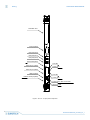
1
[Insert the picture here] Preface Thank you for choosing the CPU-71-17. Please read this manual before using the CPU-71-17 so that you may obtain the greatest benefit from using the device. This manual presents the specifications, functions, and method of use of the CPU-71-17. Eurotech has made every effort to carefully inspect each product and has taken great care to package and to ship the product. In the unlikely event of the product’s failure to operate normally due to problems in shipping or otherwise, the company will repair or replace the product at its own responsibility. If you have any questions, contact your local Eurotech Sales Office. Trademarks All trademarks both marked and unmarked appearing in this document are the property of their respective owners. This document does not give permission to the implementation of patents or other rights held by Eurotech or third parties. Revision history Revision 1 © 2014 Eurotech Description First release Date 2 September 2014 Advme8038 USER MANUAL Table of contents Table of contents Preface ...................................................................................................................................................................... 2 Trademarks ............................................................................................................................................................... 2 Revision history ......................................................................................................................................................... 2 Table of contents ........................................................................................................................................................ 3 1. Important User Information .................................................................................................................................... 7 1.1 Safety Notices and Warnings .............................................................................................................................. 7 1.2 Life Support Policy .............................................................................................................................................. 9 1.3 Warranty .............................................................................................................................................................. 9 1.4 RoHS ................................................................................................................................................................... 9 1.5 Technical Assistance........................................................................................................................................... 9 1.6 Conventions ........................................................................................................................................................ 9 1.7 Electromagnetic Compatibility ........................................................................................................................... 10 2. Summary ............................................................................................................................................................... 11 3. Specifications ....................................................................................................................................................... 12 4. Block Diagram ....................................................................................................................................................... 14 5. Setting.................................................................................................................................................................... 15 5.1. Panel Components ........................................................................................................................................... 15 5.1.1. Power status / Disk access LED .............................................................................................................. 17 5.1.2. sRIO link LED .......................................................................................................................................... 17 5.1.3. Reset switch ............................................................................................................................................. 17 5.1.4. USB port .................................................................................................................................................. 17 5.1.5. RS232C serial port................................................................................................................................... 17 5.1.6. Ethernet port 1,2 ...................................................................................................................................... 17 5.1.7. PMC/XMC slot 1,2 ................................................................................................................................... 17 5.2. Sub board Components.................................................................................................................................... 18 5.2.1. USB Port .................................................................................................................................................. 18 5.2.2. DisplayPort............................................................................................................................................... 18 5.2.3. CN1,2 (main board mounting connector) ................................................................................................. 18 5.3. On board Components ..................................................................................................................................... 19 5.3.1. CN1(BIOS code writing connector) .......................................................................................................... 20 5.3.2. CN2,3(mSATA SSD socket) .................................................................................................................... 20 5.3.3. CN4(VGA connector) ............................................................................................................................... 20 5.3.4. CN5(serial port connector) ....................................................................................................................... 20 5.3.5. CN6(Ethernet connector) ......................................................................................................................... 20 5.3.6. CN7,8(Options Sub board mounting connector) ...................................................................................... 20 5.3.7. CN9 to 12(USB connector) ...................................................................................................................... 20 5.3.8. CN14(Internal control logic writing connector 1) ...................................................................................... 21 5.3.9. CN16(Internal control logic writing connector 2) ...................................................................................... 21 5.3.10. CN19(eUSB connector) ......................................................................................................................... 21 5.3.11. CN22(Internal control firmware writing connector) ................................................................................. 21 5.3.12. CN23(Internal control firmware debug connector) ................................................................................. 21 5.3.13. BT1(CMOS backup battery) ................................................................................................................... 21 5.3.14. SW1(reset switch) .................................................................................................................................. 21 5.3.15. SW2(Clear CMOS / sRIO setting) .......................................................................................................... 22 5.3.16. JP1(RTCRST pin) .................................................................................................................................. 22 5.3.17. JP2(Internal control logic writing setting jumper) .................................................................................... 22 5.3.18. P0(VXS connector) ................................................................................................................................ 22 5.3.19. J15~16,J25(XMC connector) ................................................................................................................. 22 5.3.20. J11~14, J21~24(PMC connector) .......................................................................................................... 23 3 B33036C0-MN002-00_UserMan_En_1 Table of contents Advme8038 USER MANUAL 6. Connector .............................................................................................................................................................. 24 6.1. USB Connector (USB) ...................................................................................................................................... 24 6.2. Serial ports (COM1) ......................................................................................................................................... 24 6.3. Ethernet Connector (ETHERNET1,2) ............................................................................................................... 25 6.4. VGA Connector (VGA) ..................................................................................................................................... 25 6.5. mSATA Connector (CN2) ................................................................................................................................. 26 6.6. PMC J11(J21) Connector ................................................................................................................................. 27 6.7. PMC J12(J22) Connector ................................................................................................................................. 28 6.8. PMC J13(J23) Connector ................................................................................................................................. 29 6.9. PMC J14 Connector ......................................................................................................................................... 30 6.10. PMC J24 Connector ....................................................................................................................................... 31 6.11. XMC J15 Connector ....................................................................................................................................... 31 6.12. XMC J16 Connector ....................................................................................................................................... 32 6.13. XMC J25 Connector ....................................................................................................................................... 32 6.14. VME P1 Connector ......................................................................................................................................... 33 6.15. VME P2 Connector ......................................................................................................................................... 34 6.16. VXS P0 Connector ......................................................................................................................................... 34 6.17. eUSB CN19 Connector .................................................................................................................................. 35 7. Address Map ......................................................................................................................................................... 36 7.1. I/O space .......................................................................................................................................................... 36 7.2. Memory space .................................................................................................................................................. 37 7.3. PCI Device ....................................................................................................................................................... 39 7.4. SMBus Address Map ........................................................................................................................................ 39 8. sRIO ....................................................................................................................................................................... 40 9. VME bus ................................................................................................................................................................. 41 10. BIOS Setup .......................................................................................................................................................... 42 10.1. Main Menu...................................................................................................................................................... 42 10.1.1. System Date .......................................................................................................................................... 42 10.1.2. System Time .......................................................................................................................................... 42 10.1.3. System Information ................................................................................................................................ 42 10.1.4. Boot Features ........................................................................................................................................ 43 10.1.5. Network Stack ........................................................................................................................................ 44 10.1.6. Error Manager ........................................................................................................................................ 44 10.2. Advanced Menu ............................................................................................................................................. 45 10.2.1. Select Language .................................................................................................................................... 45 10.2.2. Silicon Information ................................................................................................................................. 45 10.2.3. ACPI Configuration ................................................................................................................................ 45 10.2.4. Processor Configuration......................................................................................................................... 46 10.2.5. Peripheral Configuration ........................................................................................................................ 48 10.2.6. HDD Configuration ................................................................................................................................. 48 10.2.7. Memory Configuration ............................................................................................................................ 49 10.2.8. System Agent (SA) Configuration .......................................................................................................... 49 10.2.9. South Bridge Configuration .................................................................................................................... 53 10.2.10. Network Configuration.......................................................................................................................... 56 10.2.11. SuperIO 1 Configuration ...................................................................................................................... 56 10.2.12. SMBIOS Event Log .............................................................................................................................. 56 10.2.13. AMT Configuration ............................................................................................................................... 57 10.2.14. ME Configuration ................................................................................................................................. 57 10.2.15. Thermal Configuration.......................................................................................................................... 58 10.2.16. ICC Configuration ................................................................................................................................ 59 10.2.17. Intel Rapid Start Technology ................................................................................................................ 59 4 B33036C0-MN002-00_UserMan_En_1 Advme8038 USER MANUAL Table of contents 10.3. Security Menu ................................................................................................................................................ 60 10.4. BootMenu ....................................................................................................................................................... 60 10.5. Misc Menu ...................................................................................................................................................... 60 10.6. Exit Menu ....................................................................................................................................................... 60 Notes .......................................................................................................................................................................... 61 5 B33036C0-MN002-00_UserMan_En_1 Advme8038 USER MANUAL Important User Information 1. Important User Information In order to lower the risk of personal injury, electric shock, fire, or equipment damage, users must observe the following precautions as well as good technical judgment, whenever this product is installed or used. All reasonable efforts have been made to ensure the accuracy of this document; however, Eurotech assumes no liability resulting from any error/omission in this document or from the use of the information contained herein. Eurotech reserves the right to revise this document and to change its contents at any time without obligation to notify any person of such revision or changes. Reproduction of all or part of this document without Eurotech’s permission is prohibited. 1.1 Safety Notices and Warnings The following general safety precautions must be observed during all phases of operation, service, and repair of this equipment. Failure to comply with these precautions or with specific warnings elsewhere in this manual violates safety standards of design, manufacture, and intended use of the equipment. Eurotech assumes no liability for the customer’s failure to comply with these requirements. The safety precautions listed below represent warnings of certain dangers of which Eurotech is aware. You, as the user of the product, should follow these warnings and all other safety precautions necessary for the safe operation of the equipment in your operating environment. Alerts that can be found throughout this manual The following alerts are used within this manual and indicate potentially dangerous situations. Danger, electrical shock hazard: Information regarding potential electrical shock hazards: Personal injury or death could occur. Also damage to the system, connected peripheral devices, or software could occur if the warnings are not carefully followed. Appropriate safety precautions should always be used, these should meet the requirements set out for the environment that the equipment will be deployed in. Warning: Information regarding potential hazards: Personal injury or death could occur. Also damage to the system, connected peripheral devices, or software could occur if the warnings are not carefully followed. Appropriate safety precautions should always be used, these should meet the requirements set out for the environment that the equipment will be deployed in. Information and/or Notes: These will highlight important features or instructions that should be observed. Protect the device from vibration and impact Do not place the product in a location where it can fall or can be subject to vibration or impact because this may cause device failure. Do not modify the device For safety reasons, under no circumstances should you modify the device. Eurotech will not repair products that have been modified. 7 B33036C0-MN002-00_UserMan_En_1 Important User Information Advme8038 USER MANUAL Protect the product from water and chemicals Contact between the product and water or chemicals can result in product failure, electrocution, or fire. Protect the product from foreign material Make sure that foreign material does not get into the product during use, storage, or transport because this can result in product failure. Use precautions in handling to ensure that you are not injured The sharp projections on this product may cause injury. Take care in handling this product in order to avoid injury. Do not disassemble the product In order to maintain guaranteed product performance, do not disassemble this product under any circumstances. Keep the product away from radios and TVs Do not use the product near radios, television sets, or other devices generating strong magnetic or electrical fields. This could result in failure or malfunction. Keep the product away from flame, humidity, and direct sunlight Do not use or store the product in any of the following locations, as this could result in product failure: Places where there is fire Locations high in humidity or exposed to rain Locations exposed to direct sunlight Dusty or dirty locations Locations containing excessive water or chemical vapors Install the product in well-ventilated locations Install the product in well-ventilated locations to efficiently disperse heat generated by the product. Remove the power plug from the receptacle when not using the product Turn off the main switch and remove the power plug from the receptacle when not using the product or when there is the risk of lightning strike. Use the device within rated parameters Be sure to use the product within the ratings specified in this manual. Failure to do so may result in malfunction. Use care when cleaning the product If the product becomes dirty, wipe it with a dry soft cloth. A thinned neutral cleaner may be used if the product is particularly dirty. Do not use benzene, thinners, or other solvents under any circumstances. Ground the product in order to prevent electrocution Be sure to ground the product by connecting it to a 3-pole AC receptacle or by using an AC receptacle having a grounding terminal. Dispose of the product properly Use appropriate methods for handling industrial wastes when disposing of this product. Wire the product correctly Failure to wire the product correctly can result in malfunction or fire. Read this manual and wire the product correctly. 8 B33036C0-MN002-00_UserMan_En_1 Advme8038 USER MANUAL Important User Information Use antistatic precautions This product comprises electronic parts that are highly susceptible to static electricity. Static electricity can cause the product to malfunction. Take care not to touch any of the terminals, connectors, ICs, or other parts with the hands. Do not use a malfunctioning product Stop using the product if you believe it is malfunctioning. Continuing to use a malfunctioning product can cause the malfunction to spread to other products and can cause short circuits or fire. 1.2 Life Support Policy Eurotech products are not authorized for use as critical components in life support devices or systems without the express written approval of Eurotech. 1.3 Warranty For warranty terms and conditions users should contact their local Eurotech Sales Office. Refer to the back covers of this manual for full contact details. 1.4 RoHS This device, including all its components, subassemblies and the consumable materials that are an integral part of the product, has been manufactured in compliance with the European directive 2011/65/EU known as the RoHS directive (Restrictions on the use of certain Hazardous Substances). This directive targets the reduction of certain hazardous substances previously used in electrical and electronic equipment (EEE). In the case of having VXS, contact the sales staff. 1.5 Technical Assistance If you have any technical questions, cannot isolate a problem with your device, or have any enquiry about repair and returns policies, contact your local Eurotech Technical Support Team. See the back cover for full contact details. Transportation When transporting any module or system, for any reason, it should be packed using anti-static material and placed in a sturdy box with enough packing material to adequately cushion it. Warning: Any product returned to Eurotech that is damaged due to inappropriate packaging will not be covered by the warranty. 1.6 Conventions The following table describes the conventions for signal names used in this document. Convention GND # + NC RSVD Explanation Digital ground plane Active low signal Positive signal in differential pair Negative signal in differential pair No connection Use is reserved to Eurotech 9 B33036C0-MN002-00_UserMan_En_1 Important User Information Advme8038 USER MANUAL 1.7 Electromagnetic Compatibility This product is intended for industrial assembly only and is not for commercial use. Therefore, this product is not an apparatus and so does not need to be subject to the EMC Directive. 10 B33036C0-MN002-00_UserMan_En_1 Advme8038 USER MANUAL Summary 2. Summary CPU-71-17 is a single board computer equipped with the 4th generation Intel Core TM mobile processor conforming to VXS/VME bus standards. VXS enables high-speed serial communication while maintaining the existing VME bus properties. In VXS, communication speed between boards becomes theoretically 6.25 times faster than that of VME. The 4th Intel Core TM mobile processor uses 22nm process 3D transistor technology realizing improved performance of floating-point calculations by Intel AVX2.0 and enhanced security operation by Intel AES-NI. The main memory contains memory with DDR3L ECC functions on board which assures high reliability. The maximum memory capacity is 8GB. One bit error among 72 bits can be automatically corrected and 2 bit errors can be detected. I/O ports consist of mSATA, USB2.0, eUSB, XMC, PMC, Gigabit Ethernet, and Serial ports. As options, 3 ports to USB2.0, VGA or DisplayPort, and USB3.0 can be added. OS currently supports Windows 7 and Wind River VxWorks. Also it will support Windows 8 and WindRiver Linux. CPU-71-17 has the following features: 4th Generation Intel® Core TM Processor ECC supported DDR3 memory direct-mounted on board (maximum capacity of memory: 8GB) Max 4 ports of USB2.0 interface 1 socket of mSATA interface 2 ports of 10/100/1000BASE-T ethernet 1 port RS-232C serial poart(RJ-45 connector) 2 slots PMC/XMC single size 1 port Analog VGA interface (*1) 1 port DisplayPort (*1) VME interface using the IDT PCI-VME bridge Tsi148 VXS interface using the IDT PCIe-sRIO bridge Tsi721 (*1) RoHS compliant (2011/65/EU) (*2) *1 *2 : Mounting option : In the case of having VXS, contact the sales staff. 11 B33036C0-MN002-00_UserMan_En_1 Specifications Advme8038 USER MANUAL 3. Specifications Table 1. Board Specifications Item CPU Specifications Processor Processor operation frequency L1 cache L2 cache L3 cache Memory Boot ROM Main Memory On board IO mSATA eUSB PMC/XMC slot 1 PMC/XMC slot 2 Front I/O VME P1/P2 connector Ethernet Serial port USB Options 1 (*2) <CPU-71-17-Opt1> Options 2 (*2) <CPU-71-17-Sub> VMEbus VXS P0 connector VXS Display・operation section Front panel On board RAS function Watchdog timer Temperature monitor 1. Intel○CoreTM i7-4700EQ processor 4 core/8 threads 37W Ⓡ 2. Intel○ CoreTM i5-4402E processor 2 core /4 threads 25W Ⓡ 3. Intel○ CoreTM i3-4102E processor 2 core /4 threads 25W <Mounting option> 1. 2.4GHz (Turbo Boost, 3.4GHz max) 2. 1.6GHz (Turbo Boost, 2.7GHz max) 3. 1.6GHz 1 to 3. 32kB for data, 32kB for instruction (per core) 1 to 3. 256kB for data and instruction (per core) 1. 6MB for data and instruction (shared by all cores) 2,3. 3MB for data and instruction (shared by all cores) SPI-FLASH memory, 16MB DDR3L-1600 SDRAM 4GB or 8GB ECC function support < Mounting option > It supports ECC, automatically corrects 1-bit error, and also detects 2-bit errors. Serial ATA Revision 3.0 OS can be booted. USB2.0 OS can be booted. IEEE1386.1 / VITA42.3 / VITA42.2, Single size (PMC) PCI32/64bit, 33/66MHz, VIO3.3V (XMC) PCIe Gen2 X4 lanes (*1) , sRIO Gen2 4X lanes < Maximum power supply >: Up to15W in total for 2 slots < Maximum supply current >: As for 3.3V, up to 4A in total for 2 slots IEEE1386.1 / VITA42.3, Single size (PMC) PCI32/64bit, 33/66MHz, VIO3.3V (XMC) PCIe Gen2 X8 lanes (*1) < Maximum power supply >: Up to15W in total for 2 slots < Maximum supply current >: As for 3.3V, up to 4A in total for 2 slots 10/100/1000BASE-T, RJ-45 connector, 2 ports RS232C, RJ-45 connector, 1 port USB2.0, USB-Type A connector, 1 port USB2.0: 3 ports, USB2.0, USB-Type A connector Analog VGA: 1 port, 15 pins are high density D-sub connector USB3.0: 1 port, USB3.0, USB-Type A connector DisplayPort: 1 port, DisplayPort connector VMEbus C.3 ANSI/VITA1-1994 VME64 ANSI/VITA1.1-1997 VME64 Extensions ANSI/VITA1.5-2003 2eSST ANSI/VITA41.2-2006 VXS Serial RapidIO Serial Rapid IO Gen2 4x: 2 ports 5.0, 3.125, 2.5, 1.25GBaud Power status / Disk access LED(Green / Orange) sRIO link LED(Orange / Green) Reset switch Clear CMOS jumper Post Battery holder for holding date and time data (CR2032) QM87 built-in function is used. CPU junction temperature, PCH junction temperature, Board surface temperature (upper part, lower part) can be monitored. Ⓡ 12 B33036C0-MN002-00_UserMan_En_1 Advme8038 USER MANUAL Item Power source specifications Specifications Specifications Power Supply Current consumption Battery Mechanical Specifications Form Factor Powered from the P1 / P2 connector DC5V±5% (DC12V±5%) (DC-12V±5%) To use +12V or -12V power source at PMC slot, the same power supply is separately needed.) DC5V: 7.6A max (4402E, nVXS) DC5V: 9.2A max (4700EQ, nVXS) DC5V:11.6A max (4700EQ, VXS) (Without PMC / XMC both) Lithium primary battery CR2032 is used. Backup the CMOS area and real-time clock. Turn off the power for about three years retention. (25℃ at the time) Low battery voltage alarm bit. It is available without a battery. 6U, 4HP(1slot width) Ejector handle is used for the panel handle. 500g Weight Operating 0 to 60℃(Air flow 2m/s or more) (*3) temperature range Operating humidity Under 95%RH(No condensation) range Storage temperature -40 to 85℃ range Storage humidity Under 95%RH(No condensation) range RoHS Compliant(2011/65/EU)(*4) : Contact us for connecting PCI Express Gen3 device. : When option 1 or option 2 is chosen, PMC/XMC slot 2 cannot be used. Environmental specifications Other *1 *2 *3 : When selecting Corei7 4700EQ and using it at upper limit temperature 60℃, an air flow of 3m/s *4 or more is required. : In the case of having VXS, contact the sales staff. Table 2. Board Product Number Contents Product Number Corei7 4700EQ, 8GB, VXS, PMC/XMC x2, USB x1 CPU-71-17 Std (4700EQ,8GB,VXS) (*1) Corei7 4700EQ, 4GB, VXS none, PMC/XMC x2, USB x1 CPU-71-17 Std (4700EQ,4GB,nVXS) (*1,2) Corei5 4402E, 4GB, VXS none, PMC/XMC x1, USB x4,VGA CPU-71-17 Opt1(4402E,4GB,nVXS) (*2) Sub board CPU-71-17 Sub *1 : eUSB is not equipped to Corei7 4700EQ. *2 : VXS connector and sRIO I/F (TSI721, CPS1616) are not equipped in case of no VXS. 13 B33036C0-MN002-00_UserMan_En_1 Block Diagram Advme8038 USER MANUAL 4. Block Diagram CPU-71-17 Block Diagram is shown in Figure.1. VXS(P0) Connector 4x (Gen2) CPS1616 SRIO Switch 4x (Gen2) 4x (Gen2) 4x 72 (Gen2) PCIe-SRIO Bridge(Tsi721) PMC/XMC Slot1 PMC/XMC Slot2 x4 (Gen2) 4th Generation Intel Processor +ECC 6M or 3M cache 37W or 25W PCIe x4 (Gen2) PCIe x8 (Gen2) 64 72 PCIe DDR3L-1600 2GB(4GB) With ECC Gen2 DMI x4 x2 PCI33/66MHz DDR3L-1600 2GB(4GB) With ECC Front I/O DisplayPort FDI 64 DMI Intel QM87 PCH 64 PCIe-PCIX Bridge USB 3.0 USB x4 (Gen1) USB USB 2.0 PCIe x1 PCIe 32 GbE Ethernet 82574 GbE Super I/O COM1 4 FPGA LPC PCIe Tsi148 PCI-VME Bridge LPC 64 64 VME64(P1,2) Connector Ethernet Clarksville 46 PMC Slot1 (P4V2/64ac) PMC Slot2 (P4V2/46dz) x1 4 USB USB 2.0 USB USB 2.0 USB USB 2.0 VGA VGA SATA mSATA USB eUSB (*1) SPI BIOS SMB Therm.MON GPIO DSW On Board I/O Clock Generator Power Regulators Reset-SW Opt1 VXS Sub *1 : When Corei7 4700EQ is selected, eUSB cannot be used. Figure 1. Block Diagram 14 B33036C0-MN002-00_UserMan_En_1 Advme8038 USER MANUAL Setting 5. Setting 5.1. Panel Components Figure 2 indicates CPU-71-17-Std board component, and Figure 3 indicates CPU-71-17-Opt1 board component. PMC/XMC slot 1 PMC/XMC slot 2 Reset switch (SW1) Link LED Ethernet port 2(CN6) RESET ETHERNET1 Ethernet port 1(CN6) USB port(CN9) ETHERNET2 RS232C serial port(CN5) Activity LED USB Link LED Activity LED P/DA SIO sRIO Power status / Disk access LED sRIO Link LED Figure 2. CPU-71-17-Std panel components 15 B33036C0-MN002-00_UserMan_En_1 Setting Advme8038 USER MANUAL PMC/XMC slot 1 VGA port(CN4) VGA USB port(CN12) USB port(CN11) USB1 USB port(CN10) USB2 USB3 Reset switch(SW1) Link LED Ethernet port 2(CN6) RESET ETHERNET1 Ethernet port 1(CN6) USB port(CN9) ETHERNET2 RS232C serial port(CN5) Activity LED USB4 Link LED Activity LED P/DA SIO sRIO Power status / Disk access LED sRIO Link LED Figure 3. CPU-71-17-Opt1 panel components 16 B33036C0-MN002-00_UserMan_En_1 Advme8038 USER MANUAL Setting 5.1.1. Power status / Disk access LED This is the status LED indicating the board’s energized condition and mSATA/eUSB’s disk access. LED indicator meanings are as follows. Status Power off Power on Disk access Power status / Disk access LED OFF Green ON Orange ON 5.1.2. sRIO link LED This is the LED indicating VXS’s sRIO link status. The LED indicator meanings are as follows. Status No link Single-channel link Both channels link sRIO link LED OFF Orange ON Green ON 5.1.3. Reset switch Pressing the reset switch executes board reset in a single action. When the reset switch is pushed, both this board and VME buses are reset. VME bus setting (reset/ no reset) is selectable according to DIP switch (SW3) setting. 5.1.4. USB port This is the USB port connector. This port is controlled by QM87 PCH-integrated USB controller. 5.1.5. RS232C serial port This is the RS232C serial port connector. This port is controlled by Super I/O. Supported baud rate is 115,200bps maximum. When you connect or disconnect to this connector please turn off the power. 5.1.6. Ethernet port 1,2 10/100/1000BASE-T Ethernet connector. The link LED turns on when the link is established, and the activity LED turns on in Yellow when transmission and reception take place. 5.1.7. PMC/XMC slot 1,2 It is a slot for equipping with a PMC/XMC module. A blank panel is provided so that the inside of the board is not exposed when a PMC/XMC module is not installed. Remove this when using a PMC/XMC module. 17 B33036C0-MN002-00_UserMan_En_1 Setting Advme8038 USER MANUAL 5.2. Sub board Components Figure 4 and Figure 5 indicate CPU-71-17-Sub board components. USB 3.0 DisplayPort USB3.0 Port(CN4) DisplayPort(CN3) Figure 4. CPU-71-17 Sub panel components CN2 CN1 CN3 CN4 CPU-71-17 Figure 5. Component placement diagram o CN1,2 o CN3 o CN4 : main board mounting connector : DisplayPort connector : USB3.0 port connector 5.2.1. USB Port This is the USB 3.0 port connector. This port is controlled by QM87 PCH-integrated controller. USB3.0’s SSC is set to OFF. 5.2.2. DisplayPort This is the DisplayPort connector. This port is controlled by CPU-integrated display controller. It corresponds to DisplayPort 1.1a, and its maximum resolution is 2560x1600. 5.2.3. CN1,2 (main board mounting connector) It interfits CN7, 8 of CPU-71-17 main board. 18 B33036C0-MN002-00_UserMan_En_1 Advme8038 USER MANUAL Setting 5.3. On board Components Figure 6 indicate CPU-71-17 component placement diagram. SW1 CN5 CN9 CN10 CN6 CN11 CN12 CN4 CN16 JP1 BT1 CN14 CN7 CN8 CN3 CN2 JP2 SW2 CN19 J25 J23 CN1 J24 P0 P2 J16 J15 J21 J13 J11 J22 J14 J12 CN22 CN23 A0 P1 Figure 6. Component placement diagram : BIOS code writing connector (5.3.1. CN1(BIOS code writing connector) page 20) : mSATA SSD socket(5.3.2. CN2,3(mSATA SSD socket) page 20) : VGA connector (5.3.3. CN4(VGA connector) page 20) : Serial port connector (5.3.4. CN5(serial port connector) page 20) : Ethernet connector (5.3.5. CN6(Ethernet connector) page 20) : Options Sub Board mounting connector (5.3.6. CN7,8(Options Sub board mounting connector) page 20) o CN9 to 12 : USB port connector (5.3.7. CN9 to 12(USB connector) page 20) o CN14 : Internal control logic writing connector 1 (5.3.8. CN14(Internal control logic writing connector 1) page 21) o CN16 : Internal control logic writing connector 2 (5.3.9. CN16(Internal control logic writing connector 2) page 21) o CN19 : eUSB connector (5.3.10. CN19(eUSB connector) page 21) o CN22 : Internal control firmware writing connector (5.3.11. CN22(Internal control firmware writing connector) page 21) o o o o o o CN1 CN2,3 CN4 CN5 CN6 CN7,8 19 B33036C0-MN002-00_UserMan_En_1 Setting o CN23 o o o o o BT1 SW1 SW2 JP1 JP2 o o o o o o o A0 P0 P1,2 J15,16 J25 J11-14 J21-24 Advme8038 USER MANUAL : Internal control firmware writing connector (5.3.12. CN23(Internal control firmware debug connector) page 21) : CMOS backup battery (5.3.13. BT1(CMOS backup battery) page 21) : Reset switch(5.3.14. SW1(reset switch) page 21) : Clear CMOS / sRIO setting (5.3.15. SW2(Clear CMOS / sRIO setting) page 22) : RTCRST pin(5.3.16. JP1(RTCRST pin)page 22) : Internal control logic writing setting jumper (5.3.17. JP2(Internal control logic writing setting jumper) page 22) : VXS positioning socket : VXS connector (5.3.18. P0(VXS connector) page 22) : VME bus connector : XMC1 connector (5.3.19. J15~16,J25(XMC connector) page 22) : XMC2 connector (5.3.19. J15~16,J25(XMC connector) page 22) : PMC1 connector (5.3.20. J11~14, J21~24(PMC connector) page 23) : PMC2 connector (5.3.20. J11~14, J21~24(PMC connector) page 23) 5.3.1. CN1(BIOS code writing connector) CN1 is a connector for writing BIOS code to the on-board SPI-FLASH memory. Do not connect anything during normal operation. 5.3.2. CN2,3(mSATA SSD socket) CN2,3 are the mSATA SSD socket. Use SSD that conforms to Serial ATA mSATA standard. Do not conduct hot swapping. Part height of mSATA upper face is up to 2mm. 5.3.3. CN4(VGA connector) CN4’s maximum resolution is 1920x1080 using the VGA connector. It is an option , and PMC/XMC slot 2 cannot be used when installed. Do not conduct hot swapping. 5.3.4. CN5(serial port connector) CN5 is the RS232C serial port connector. 5.3.5. CN6(Ethernet connector) CN6 is the Ethernet connector of two ports. 5.3.6. CN7,8(Options Sub board mounting connector) CN7,8 are the options sub PCB mounting connector. By mounting an optional sub board, a DisplayPort output port and a USB3.0 host interface port can be added. 5.3.7. CN9 to 12(USB connector) CN9 to 12 is the USB host interface connector. Power current capacity that can be supplied to USB device is up to 500mA for each port. Exceeding this value, the overcurrent protection circuit activates and the USB device connected to the port cannot be used. When overcurrent factors are removed, the protection circuit automatically recovers and the port can be used again. CN10 to 12 are optional. It is a PMC/XMC slot 2 cannot be used when installed. 20 B33036C0-MN002-00_UserMan_En_1 Advme8038 USER MANUAL Setting 5.3.8. CN14(Internal control logic writing connector 1) CN14 is a connector for writing programmable logic in the board. Do not connect anything during normal operation. 5.3.9. CN16(Internal control logic writing connector 2) CN16 is a connector for writing programmable logic in the board. Do not connect anything during normal operation. 5.3.10. CN19(eUSB connector) CN19 is an eUSB host interface connector. It can be connected to a 5V, standard profile Embedded USB Drive. ACT# pin’s signalling level is 3.3V LVTTL and has 10kΩ on board pull-up. Do not conduct hot swapping. 5.3.11. CN22(Internal control firmware writing connector) CN22 is a connector for writing micro controller in the board. Do not connect anything during normal operation. 5.3.12. CN23(Internal control firmware debug connector) CN23 is a connector to debug the micro controller on the board. Do not connect anything during normal operation. 5.3.13. BT1(CMOS backup battery) BT1 is a holder to mount the battery for CMOS backup. Battery to be used is CR2032. Be aware of the following when mounting and removing the battery. 1. Do not touch the battery with a conductive object such as a screw driver. Using a conductive object is dangerous as it can cause the circuit or battery to short circuit. 2. Do not strongly impact the battery such as by dropping it. 3. Before replacing the battery, turn off the power source, and install the battery paying attention to the battery polarity. CPU-71-17 is equipped with battery under voltage detection, and battery’s status can be confirmed from PCH’s GPIO34(GP_LVL2 register). State Battery voltage is normal. Battery voltage is low. PCH GPIO34 ‘1’ = High ‘0’ = Low When using this without a battery, the following should be noted. o CMOS information, time, and date are cleared when power is turned off. o Do not mix CPU-71-17 with battery/without battery in the same rack. 5.3.14. SW1(reset switch) SW1 is the board reset switch. Pressing the SW1 executes board reset in a single action. 21 B33036C0-MN002-00_UserMan_En_1 Setting Advme8038 USER MANUAL 5.3.15. SW2(Clear CMOS / sRIO setting) SW2 setting is indicated in Table 3. Bit8 is a switch to return BIOS’s individual settings to initial values. Bit8 usage is not usually required, so use it with power OFF. Only when the BIOS setup screen is not displayed due to improper operations, etc., clear CMOS as described below. (1) Turn off power to the CPU-71-17. (2) Turn on SW2 Bit8. (3) When the CPU-71-17 turns on, BIOS’s individual settings start up at initial values. (4) Turn off power and turn off the SW2 Bit8. Bit1 to 7 are switches to set sRIO bridge Tsi721. When Bit1 is turned ON, SLAVE activates, and when OFF, HOST activates. Bit2 is the initial value setting of destination ID. Turning ON when Slave is activating, it becomes 0xFE, and turning OFF, it becomes 0xFF. Turning ON when Host is activating, it becomes 0x00, and turning OFF, it becomes 0x01. When turning Bit3 ON, I2C EEPROM is read when starting up to perform register settings. It is usually used with ON. Bit4-6 is communication speed setting. Bit7 is sRIO boot setting. It is usually used with OFF. Table 3. SW2 Setting SW2 Bit1 Bit2 Bit3 Function SP_HOST SP_DEVID I2C_LOAD Bit4 Bit5 Bit6 STRAP_RATE[0] STRAP_RATE[1] STRAP_RATE[2] Bit7 Bit8 SR_BOOT CMOS_CLEAR [2] 1 1 1 0 ON(1) OFF(0) SLAVE HOST 0/FE 1/FF Enable Disable [1] [0] 1 1 1.25 Gbaud 1 0 2.5 Gbaud 0 1 5.0 Gbaud 1 0 3.125 Gbaud AUTO MANUAL Enable Disable 5.3.16. JP1(RTCRST pin) JP1 is connected to QM87’s RTCRST#. Do not connect anything during normal operation. 5.3.17. JP2(Internal control logic writing setting jumper) JP2 is a jumper used when writing the programmable logic in the board. Do not connect anything during normal operation. 5.3.18. P0(VXS connector) This is a connector to connect with VXS back plane. In CPU-71-17, sRIO signal is connected. It can communicate with payload card and switch card that conform to VITA41.2 standards. This is not equipped when VXS does not exist. 5.3.19. J15~16,J25(XMC connector) This is a connector to install XMC module. PCI Express Gen1 and Gen2 XMC module can be used. XMC slot 1 corresponds to x4 links. XMC slot 2 corresponds to x8 links. When VXS exists, sRIO signal is connected to XMC slot 1. (J16 connector) To use the XMC module using the P16 connector with CPU-71-17, confirm the signal is for sRIO. When VXS does not exist, J16 connector is not equipped. 22 B33036C0-MN002-00_UserMan_En_1 Advme8038 USER MANUAL Setting 5.3.20. J11~14, J21~24(PMC connector) This is a connector to install PMC module. PCI bus in this board is directly connected to PMC connector. Signalling voltage 3.3V PMC module can be used with this board. Refer to Table 1: Specification List for details. PMC slot 1’s use I/O pin (equivalent to J14) connects all 64 pins to A and C columns of P2 connector. Also, PMC slot 2’s I/O pin (equivalent to J24) connects 46 pins to D and Z columns of P2 connector. Refer to Chapter 6.6 to 6.10 for each pin assignment. When using the PMC module using P4 connector signal, confirm how corresponding signals on the back plane are connected before using. 23 B33036C0-MN002-00_UserMan_En_1 Connector Advme8038 USER MANUAL 6. Connector 6.1. USB Connector (USB) Connector used: JST UBAL-4R-D14-4S(LF)(SN) Name +5V -DATA +DATA GND Pin 1 2 3 4 4 3 2 1 (Panel) 6.2. Serial ports (COM1) Connector used: HIROSE TM11R-5M2-88-LP(33) Name DCD RTS GND TXD RXD GND CTS DTR Pin 1 2 3 4 5 6 7 8 87654321 (Panel) 24 B33036C0-MN002-00_UserMan_En_1 Advme8038 USER MANUAL Connector 6.3. Ethernet Connector (ETHERNET1,2) Connector used: BELFUSE 0826-1X2T-23-F Name A+ AB+ C+ CBD+ D- Pin 1 2 3 4 5 6 7 8 87654321 (Panel) 6.4. VGA Connector (VGA) Connector used: JST KEY-15S-2A3A[LF][SN] Name RED GRN BLU NC GND GND GND GND 5V GND NC I2C_DAT HSYNC VSYNC I2C_CK Pin 1 2 3 4 5 6 7 8 9 10 11 12 13 14 15 5 ... 1 10 ... 6 15 ... 11 (Panel) 25 B33036C0-MN002-00_UserMan_En_1 Connector Advme8038 USER MANUAL 6.5. mSATA Connector (CN2) Connector used: JAE MM60-52B1-B1 Pin 1 2 3 4 5 6 7 8 9 10 11 12 13 14 15 16 17 18 19 20 21 22 23 24 25 26 Name NC +3.3V NC GND NC +1.5V NC NC GND NC NC NC NC NC GND NC NC GND NC NC GND NC +B +3.3V -B GND Pin 27 28 29 30 31 32 33 34 35 36 37 38 39 40 41 42 43 44 45 46 47 48 49 50 51 52 Name GND +1.5V GND TWI -A TWI +A GND GND NC GND NC +3.3V GND +3.3V NC NC GND NC NC NC +1.5V NC GND NC +3.3V 26 B33036C0-MN002-00_UserMan_En_1 Advme8038 USER MANUAL Connector 6.6. PMC J11(J21) Connector Connector used: KYOCERA ELCO Pin 1 3 5 7 9 11 13 15 17 19 21 23 25 27 29 31 33 35 37 39 41 43 45 47 49 51 53 55 57 59 61 63 24-5015-064-100-861+ Name NC GND INTB# BUSMODE1# INTD# GND PCICLK GND REQ# +3.3V(VIO) AD28 AD25 GND AD22 AD19 +3.3V(VIO) FRAME# GND DEVSEL# GND SDONE# PAR +3.3V(VIO) AD12 AD9 GND AD6 AD4 +3.3V(VIO) AD2 AD0 GND Pin 2 4 6 8 10 12 14 16 18 20 22 24 26 28 30 32 34 36 38 40 42 44 46 48 50 52 54 56 58 60 62 64 Name -12V INTA# INTC# +5V NC NC GND GNT# +5V AD31 AD27 GND C/BE3# AD21 +5V AD17 GND IRDY# +5V LOCK# SBO# GND AD15 AD11 +5V C/BE0# AD5 GND AD3 AD1 +5V REQ64# 27 B33036C0-MN002-00_UserMan_En_1 Connector Advme8038 USER MANUAL 6.7. PMC J12(J22) Connector Connector used: KYOCERA ELCO Pin 1 3 5 7 9 11 13 15 17 19 21 23 25 27 29 31 33 35 37 39 41 43 45 47 49 51 53 55 57 59 61 63 24-5015-064-100-861+ Name +12V NC NC GND NC BUSMODE2# RST# +3.3V(VIO) PME# AD30 GND AD24 IDSEL +3.3V(VIO) AD18 AD16 GND TRDY# GND PERR# +3.3V(VIO) C/BE1# AD14 M66EN AD8 AD7 +3.3V(VIO) NC NC GND ACK64# GND Pin 2 4 6 8 10 12 14 16 18 20 22 24 26 28 30 32 34 36 38 40 42 44 46 48 50 52 54 56 58 60 62 64 Name NC NC GND NC NC +3.3V(VIO) BUSMODE3# BUSMODE4# GND AD29 AD26 +3.3V(VIO) AD23 AD20 GND C/BE2# NC +3.3V(VIO) STOP# GND SERR# GND AD13 AD10 +3.3V(VIO) NC NC GND NC NC +3.3V(VIO) NC 28 B33036C0-MN002-00_UserMan_En_1 Advme8038 USER MANUAL Connector 6.8. PMC J13(J23) Connector Connector used: KYOCERA ELCO Pin 1 3 5 7 9 11 13 15 17 19 21 23 25 27 29 31 33 35 37 39 41 43 45 47 49 51 53 55 57 59 61 63 24-5015-064-100-861+ Name NC GND C/BE6# C/BE4# +3.3V(VIO) AD63 AD61 GND AD59 AD57 +3.3V(VIO) AD55 AD53 GND AD51 AD49 GND AD47 AD45 +3.3V(VIO) AD43 AD41 GND AD39 AD37 GND AD35 AD33 +3.3V(VIO) NC NC GND Pin 2 4 6 8 10 12 14 16 18 20 22 24 26 28 30 32 34 36 38 40 42 44 46 48 50 52 54 56 58 60 62 64 Name GND C/BE7# C/BE5# GND PAR64 AD62 GND AD60 AD58 GND AD56 AD54 GND AD52 AD50 GND AD48 AD46 GND AD44 AD42 GND AD40 AD38 GND AD36 AD34 GND AD32 NC GND NC 29 B33036C0-MN002-00_UserMan_En_1 Connector Advme8038 USER MANUAL 6.9. PMC J14 Connector Connector used: KYOCERA ELCO Pin 1 3 5 7 9 11 13 15 17 19 21 23 25 27 29 31 33 35 37 39 41 43 45 47 49 51 53 55 57 59 61 63 24-5015-064-100-861+ Name J14_1(VME-P2-1C) J14_3(VME-P2-2C) J14_5(VME-P2-3C) J14_7(VME-P2-4C) J14_9(VME-P2-5C) J14_11(VME-P2-6C) J14_13(VME-P2-7C) J14_15(VME-P2-8C) J14_17(VME-P2-9C) J14_19(VME-P2-10C) J14_21(VME-P2-11C) J14_23(VME-P2-12C) J14_25(VME-P2-13C) J14_27(VME-P2-14C) J14_29(VME-P2-15C) J14_31(VME-P2-16C) J14_33(VME-P2-17C) J14_35(VME-P2-18C) J14_37(VME-P2-19C) J14_39(VME-P2-20C) J14_41(VME-P2-21C) J14_43(VME-P2-22C) J14_45(VME-P2-23C) J14_47(VME-P2-24C) J14_49(VME-P2-25C) J14_51(VME-P2-26C) J14_53(VME-P2-27C) J14_55(VME-P2-28C) J14_57(VME-P2-29C) J14_59(VME-P2-30C) J14_61(VME-P2-31C) J14_63(VME-P2-32C) Pin 2 4 6 8 10 12 14 16 18 20 22 24 26 28 30 32 34 36 38 40 42 44 46 48 50 52 54 56 58 60 62 64 Name J14_2(VME-P2-1A) J14_4(VME-P2-2A) J14_6(VME-P2-3A) J14_8(VME-P2-4A) J14_10(VME-P2-5A) J14_12(VME-P2-6A) J14_14(VME-P2-7A) J14_16(VME-P2-8A) J14_18(VME-P2-9A) J14_20(VME-P2-10A) J14_22(VME-P2-11A) J14_24(VME-P2-12A) J14_26(VME-P2-13A) J14_28(VME-P2-14A) J14_30(VME-P2-15A) J14_32(VME-P2-16A) J14_34(VME-P2-17A) J14_36(VME-P2-18A) J14_38(VME-P2-19A) J14_40(VME-P2-20A) J14_42(VME-P2-21A) J14_44(VME-P2-22A) J14_46(VME-P2-23A) J14_48(VME-P2-24A) J14_50(VME-P2-25A) J14_52(VME-P2-26A) J14_54(VME-P2-27A) J14_56(VME-P2-28A) J14_58(VME-P2-29A) J14_60(VME-P2-30A) J14_62(VME-P2-31A) J14_64(VME-P2-32A) 30 B33036C0-MN002-00_UserMan_En_1 Advme8038 USER MANUAL Connector 6.10. PMC J24 Connector Connector used: KYOCERA ELCO 24-5015-064-100-861+ Name J24_1(VME-P2-D1) J24_3(VME-P2-D2) J24_5(VME-P2-Z3) J24_7(VME-P2-D5) J24_9(VME-P2-D6) J24_11(VME-P2-Z7) J24_13(VME-P2-D9) J24_15(VME-P2-D10) J24_17(VME-P2-Z11) J24_19(VME-P2-D13) J24_21(VME-P2-D14) J24_23(VME-P2-Z15) J24_25(VME-P2-D17) J24_27(VME-P2-D18) J24_29(VME-P2-Z19) J24_31(VME-P2-D21) J24_33(VME-P2-D22) J24_35(VME-P2-Z23) J24_37(VME-P2-D25) J24_39(VME-P2-D26) J24_41(VME-P2-Z27) J24_43(VME-P2-D29) J24_45(VME-P2-D30) NC NC NC NC NC NC NC NC NC Pin 1 3 5 7 9 11 13 15 17 19 21 23 25 27 29 31 33 35 37 39 41 43 45 47 49 51 53 55 57 59 61 63 Pin 2 4 6 8 10 12 14 16 18 20 22 24 26 28 30 32 34 36 38 40 42 44 46 48 50 52 54 56 58 60 62 64 Name J24_2(VME-P2-Z1) J24_4(VME-P2-D3) J24_6(VME-P2-D4) J24_8(VME-P2-Z5) J24_10(VME-P2-D7) J24_12(VME-P2-D8) J24_14(VME-P2-Z9) J24_16(VME-P2-D11) J24_18(VME-P2-D12) J24_20(VME-P2-Z13) J24_22(VME-P2-D15) J24_24(VME-P2-D16) J24_26(VME-P2-Z17) J24_28(VME-P2-D19) J24_30(VME-P2-D20) J24_32(VME-P2-Z21) J24_34(VME-P2-D23) J24_36(VME-P2-D24) J24_38(VME-P2-Z25) J24_40(VME-P2-D27) J24_42(VME-P2-D28) J24_44(VME-P2-Z29) J24_46(VME-P2-Z31) NC NC NC NC NC NC NC NC NC D PET0p1 GND PET0p3 GND NC GND NC GND NC GND PER0p1 GND PER0p3 GND NC GND NC GND WAKE# E PET0n1 GND PET0n3 GND NC GND NC GND NC GND PER0n1 GND PER0n3 GND NC GND NC GND ROOT0# 6.11. XMC J15 Connector Connector used: SAMTEC Pin 1 2 3 4 5 6 7 8 9 10 11 12 13 14 15 16 17 18 19 ASP-103612-02 A PET0p0 GND PET0p2 GND NC GND NC GND NC GND PER0p0 GND PER0p2 GND NC GND NC GND REFCLK+0 B PET0n0 GND PET0n2 GND NC GND NC GND NC GND PER0n0 GND PER0n2 GND NC GND NC GND REFCLK-0 C +3.3V TRST# +3.3V TCK +3.3V TMS +3.3V TDI NC TDO NC GA1 +3.3V GA2 NC MVMRO NC NC NC F +5V MRSTI# +5V NC +5V +12V +5V -12V +5V GA0 +5V MPRESENT# +5V MSDA +5V MSCL NC NC NC 31 B33036C0-MN002-00_UserMan_En_1 Connector Advme8038 USER MANUAL 6.12. XMC J16 Connector Connector used: SAMTEC Pin 1 2 3 4 5 6 7 8 9 10 11 12 13 14 15 16 17 18 19 ASP-103612-02 A S0_TD0+ GND S0_TD2+ GND NC GND NC GND NC GND S0_RD0+ GND S0_RD2+ GND NC GND NC GND NC B S0_TD0GND S0_TD2GND NC GND NC GND NC GND S0_RD0GND S0_RD2GND NC GND NC GND NC C XMC_GEN1_LINK XMC_GEN2_LINK RP_SDA RP_SCL CPS1616_TCK CPS1616_TRST# CPS1616_TDI CPS1616_TMS CPS1616_TDO TSI721_TCK TSI721_TRST# TSI721_TDI TSI721_TMS TSI721_TDO NC NC NC NC NC D S0_TD1+ GND S0_TD3+ GND NC GND NC GND NC GND S0_RD1+ GND S0_RD3+ GND NC GND NC GND NC E S0_TD1GND S0_TD3GND NC GND NC GND NC GND S0_RD1GND S0_RD3GND NC GND NC GND NC F NC NC NC NC NC NC NC NC NC NC NC NC NC NC NC NC NC NC NC 6.13. XMC J25 Connector Connector used: SAMTEC Pin 1 2 3 4 5 6 7 8 9 10 11 12 13 14 15 16 17 18 19 ASP-103612-02 A PET0p0 GND PET0p2 GND PET0p4 GND PET0p6 GND NC GND PER0p0 GND PER0p2 GND PER0p4 GND PER0p6 GND REFCLK+0 B PET0n0 GND PET0n2 GND PET0n4 GND PET0n6 GND NC GND PER0n0 GND PER0n2 GND PER0n4 GND PER0n6 GND REFCLK-0 C +3.3V TRST# +3.3V TCK +3.3V TMS +3.3V TDI NC TDO NC GA1 +3.3V GA2 NC MVMRO NC NC NC D PET0p1 GND PET0p3 GND PET0p5 GND PET0p7 GND NC GND PER0p1 GND PER0p3 GND PER0p5 GND PER0p7 GND WAKE# E PET0n1 GND PET0n3 GND PET0n5 GND PET0n7 GND NC GND PER0n1 GND PER0n3 GND PER0n5 GND PER0n7 GND ROOT0# F +5V MRSTI# +5V NC +5V +12V +5V -12V +5V GA0 +5V MPRESENT# +5V MSDA +5V MSCL NC NC NC 32 B33036C0-MN002-00_UserMan_En_1 Advme8038 USER MANUAL Connector 6.14. VME P1 Connector Connector used: HARTING Pin 1 2 3 4 5 6 7 8 9 10 11 12 13 14 15 16 17 18 19 20 21 22 23 24 25 26 27 28 29 30 31 32 0201-160-2101 Row z NC GND NC GND NC GND NC GND NC GND NC GND NC GND NC GND NC GND NC GND NC GND NC GND NC GND NC GND NC GND NC GND Row a D0 D1 D2 D3 D4 D5 D6 D7 GND SYSCLK GND DS1# DS0# WRITE# GND DTACK# GND AS# GND IACK# IACKIN# IACKOUT# AM4 A7 A6 A5 A4 A3 A2 A1 -12V +5V Row b BBSY# BCLR# ACFAIL# BGI0# BGO0# BGI1# BGO1# BGI2# BGO2# BGI3# BGO3# BR0# BR1# BR2# BR3# AM0 AM1 AM2 AM3 GND NC NC GND IRQ7# IRQ6# IRQ5# IRQ4# IRQ3# IRQ2# IRQ1# NC +5V Row c D8 D9 D10 D11 D12 D13 D14 D15 GND SYSFAIL# BERR# SYSRESET# LWORD# AM5 A23 A22 A21 A20 A19 A18 A17 A16 A15 A14 A13 A12 A11 A10 A9 A8 +12V +5V Row d +5V GND NC NC NC NC NC NC GAP# GA0# GA1# NC GA2# NC GA3# NC GA4# NC NC NC NC NC NC NC NC NC NC NC NC NC GND +5V 33 B33036C0-MN002-00_UserMan_En_1 Connector Advme8038 USER MANUAL 6.15. VME P2 Connector Connector used: HARTING Pin 1 2 3 4 5 6 7 8 9 10 11 12 13 14 15 16 17 18 19 20 21 22 23 24 25 26 27 28 29 30 31 32 0201-160-2101 Row z J24_2(PMC-P24-2) GND J24_5(PMC-P24-5) GND J24_8(PMC-P24-8) GND J24_11(PMC-P24-11) GND J24_14(PMC-P24-14) GND J24_17(PMC-P24-17) GND J24_20(PMC-P24-20) GND J24_23(PMC-P24-23) GND J24_26(PMC-P24-26) GND J24_29(PMC-P24-29) GND J24_32(PMC-P24-32) GND J24_35(PMC-P24-35) GND J24_38(PMC-P24-38) GND J24_41(PMC-P24-41) GND J24_44(PMC-P24-44) GND J24_46(PMC-P24-46) GND Row a J14_2(PMC-P14-2) J14_4(PMC-P14-4) J14_6(PMC-P14-6) J14_8(PMC-P14-8) J14_10(PMC-P14-10) J14_12(PMC-P14-12) J14_14(PMC-P14-14) J14_16(PMC-P14-16) J14_18(PMC-P14-18) J14_20(PMC-P14-20) J14_22(PMC-P14-22) J14_24(PMC-P14-24) J14_26(PMC-P14-26) J14_28(PMC-P14-28) J14_30(PMC-P14-30) J14_32(PMC-P14-32) J14_34(PMC-P14-34) J14_36(PMC-P14-36) J14_38(PMC-P14-38) J14_40(PMC-P14-40) J14_42(PMC-P14-42) J14_44(PMC-P14-44) J14_46(PMC-P14-46) J14_48(PMC-P14-48) J14_50(PMC-P14-50) J14_52(PMC-P14-52) J14_54(PMC-P14-54) J14_56(PMC-P14-56) J14_58(PMC-P14-58) J14_60(PMC-P14-60) J14_62(PMC-P14-62) J14_64(PMC-P14-64) Row b +5V GND RETRY# A24 A25 A26 A27 A28 A29 A30 A31 GND +5V D16 D17 D18 D19 D20 D21 D22 D23 GND D24 D25 D26 D27 D28 D29 D30 D31 GND +5V Row c J14_1(PMC-P14-1) J14_3(PMC-P14-3) J14_5(PMC-P14-5) J14_7(PMC-P14-7) J14_9(PMC-P14-9) J14_11(PMC-P14-11) J14_13(PMC-P14-13) J14_15(PMC-P14-15) J14_17(PMC-P14-17) J14_19(PMC-P14-19) J14_21(PMC-P14-21) J14_23(PMC-P14-23) J14_25(PMC-P14-25) J14_27(PMC-P14-27) J14_29(PMC-P14-29) J14_31(PMC-P14-31) J14_33(PMC-P14-33) J14_35(PMC-P14-35) J14_37(PMC-P14-37) J14_39(PMC-P14-39) J14_41(PMC-P14-41) J14_43(PMC-P14-43) J14_45(PMC-P14-45) J14_47(PMC-P14-47) J14_49(PMC-P14-49) J14_51(PMC-P14-51) J14_53(PMC-P14-53) J14_55(PMC-P14-55) J14_57(PMC-P14-57) J14_59(PMC-P14-59) J14_61(PMC-P14-61) J14_63(PMC-P14-63) Row d J24_1(PMC-P24-1) J24_3(PMC-P24-3) J24_4(PMC-P24-4) J24_6(PMC-P24-6) J24_7(PMC-P24-7) J24_9(PMC-P24-9) J24_10(PMC-P24-10) J24_12(PMC-P24-12) J24_13(PMC-P24-13) J24_15(PMC-P24-15) J24_16(PMC-P24-16) J24_18(PMC-P24-18) J24_19(PMC-P24-19) J24_21(PMC-P24-21) J24_22(PMC-P24-22) J24_24(PMC-P24-24) J24_25(PMC-P24-25) J24_27(PMC-P24-27) J24_28(PMC-P24-28) J24_30(PMC-P24-30) J24_31(PMC-P24-31) J24_33(PMC-P24-33) J24_34(PMC-P24-34) J24_36(PMC-P24-36) J24_37(PMC-P24-37) J24_39(PMC-P24-39) J24_40(PMC-P24-40) J24_42(PMC-P24-42) J24_43(PMC-P24-43) J24_45(PMC-P24-45) GND +5V 6.16. VXS P0 Connector Connector used: TYCO 1410147 Payload side Pin 1 2 3 4 5 6 7 8 9 10 11 12 13 14 15 Row G NC GND NC GND NC GND NC GND NC GND NC GND NC GND NC Row F GND PA_TX1GND PA_TX3GND NC GND NC GND NC GND PB_TX0GND PB_TX2GND Row E PA_TX0PA_TX1+ PA_TX2PA_TX3+ NC NC NC NC NC NC NC PB_TX0+ PB_TX1PB_TX2+ PB_TX3- Row D PA_TX0+ GND PA_TX2+ GND NC GND NC GND NC GND NC GND PB_TX1+ GND PB_TX3+ Row C GND PA_RX1GND PA_RX3GND NC GND NC GND NC GND PB_RX0GND PB_RX2GND Row B PA_RX0PA_RX1+ PA_RX2PA_RX3+ NC NC NC NC NC NC NC PB_RX0+ PB_RX1PB_RX2+ PB_RX3- Row A PA_RX0+ GND PA_RX2+ GND NC GND NC GND NC GND NC GND PB_RX1+ GND PB_RX3+ 34 B33036C0-MN002-00_UserMan_En_1 Advme8038 USER MANUAL Connector 6.17. eUSB CN19 Connector Connector used: SAMTEC TSM-105-01-S-DV-P-TR Name +5V NC -DATA NC +DATA NC GND NC NC ACT# Pin 1 2 3 4 5 6 7 8 9 10 CN19 1 3 5 7 9 2 4 6 8 10 35 B33036C0-MN002-00_UserMan_En_1 Address Map Advme8038 USER MANUAL 7. Address Map 7.1. I/O space I/O space Address Map is shown in Table 4. PCI device that can be freely configured in the memory space is not listed in this table. Table 4. I/O space Address Map Address 0000h - 001Fh 0020h - 002Dh 002Eh - 002Fh 0030h - 003Dh 0040h - 0043h 004Eh - 004Fh 0050h - 0053h 0060h 0061h 0062h - 0066h 0070h - 0077h 0080h - 0091h 0092h 0093h - 009Fh 00A0h - 00B1h 00B2h - 00B3h 00B4h - 00BDh 00C0h - 00DFh 00F0h 0170h - 0177h 01F0h - 01F7h 0200h – 020Fh 0280h – 028Fh 0376h 03F6h 04D0h - 04D1h 0CF9h PCH Registers PCH Registers PCH Register Device DMA Controller Interrupt Controller Super I/O Registers Interrupt Controller Timer/Counter LPC SIO Timer/Counter Microcontroller NMI Controller Microcontroller RTC Controller DMA Controller Reset Generator DMA Controller Interrupt Controller Power Management Interrupt Controller DMA Controller FERR# / Interrupt Controller Serial ATA Serial ATA Game port Reserved Serial ATA Serial ATA Interrupt Controller Reset Generator 36 B33036C0-MN002-00_UserMan_En_1 Advme8038 USER MANUAL Address Map 7.2. Memory space Memory space Address Map is shown in Table 5. Table 5. Memory space Address Map Device Address Main Memory (640kB) 0000 0000h ~0009 FFFFh VGA Frame Buffer (128kB) 000A 0000h ~ 000B FFFFh Boot ROM or Main Memory (192kB) 000C 0000h ~ 000D FFFFh PCH Boot ROM (SPI) (128kB) 000E 0000h ~000F FFFFh Main Memory 0010_0000h ~ TSEGMB (*1) CPU Internal Graphics TSEGMB ~TOLUD (*2) PCI Memory Range TOLUD ~DFFF FFFFh PCI Express Configuration Space(256MB) E000 0000h ~EFFF FFFFh CPU DMI Interface(236MB) F000 0000h ~FEBF FFFFh I/O APIC inside PCH FEC0 0000h ~FEC0 0040h PCH PCI Express Port 1 FEC1 0000h ~FEC1 7FFFh APIC Configuration Space FEC1 8000h ~FEC4 7FFFh PCI Express Port 8 PCH FEC4 8000h ~FEC4 FFFFh APIC Configuration Space FEC5 0000 ~ FEC7 FFFFh CPU APIC FEC8 0000h ~FECF FFFFh CPU High Precision Event Timers FED0 X000h ~ FED0 X3FFh (*3) PCH TPM on LPC FED4 0000h ~FED4 BFFFh FED0 0000h ~FEDF FFFFh PCI Memory Range (subtractive decode) MSI Interrupt Memory Space FEE0 0000h ~FEEF FFFFh CPU FEF0 0000h ~ FEFF FFFFh PCI Memory Range Boot ROM(SPI) (16MB) FF00 0000h ~ FFFF FFFFh PCH *1 : TSEGMB(TSEG Memory Base address) Refer to the data sheet of the CPU for more information. *2 : TOLUD (Top of Low Usable physical memory) Register is automatically set depending on the PCI memory device. Change BIOS setting to manual set. *3 : High Precision Timer Configuration It can be set with the register. 37 B33036C0-MN002-00_UserMan_En_1 Address Map Advme8038 USER MANUAL Table 6. Device list that uses memory space Use area 128kB in 4GB 1kB in 4GB 1kB in 4GB 1kB in 4GB 64kB in 4GB 64kB in 4GB 16kB in 4GB 32Bytes in 64bit address 2kB in 64kB to 4GB Memory Base/Limit in 4GB Prefetchable Memory Base/Limit in 64bit address 4kB in 64bit address 4kB in 64bit address 4kB 32kB 4kB 0 to 512MB in Main Memory 0 to 2MB in Main Memory 128MB, 256MB, 512MB *1 Device PCH LAN Controller LAN Controller USB EHCI Controller USB EHCI Controller USB xHCI Controller LPC Root Complex Register Block SMBus SATA Host Controller PCI Express Root Ports 1,8 PCI Express Root Ports 1,8 CPU (D0) CPU (D2) 64kB in 4GB 16MB in 4GB PCI-VME 256MB in 4GB (128MB,512MB) (*1) Bridge 256MB in 4GB (128MB,512MB) (*1) : Use area can be changed. Contact us for details. Thermal Reporting Thermal Reporting PxP registers MCH registers DMI registers Graphics Mode Select GTT Graphics Memory Internal graphics translation A16 Memory Address Space A24 Memory Address Space A32 Memory Address Space1 A32 Memory Address Space2 38 B33036C0-MN002-00_UserMan_En_1 Advme8038 USER MANUAL Address Map 7.3. PCI Device PCI devices are shown in Table 7. Table 7. List of PCI devices Device number 00h 01h Function Device Bus number number 00h CPU Host and DRAM Controller 00h 00h PCI Express Controller (XMC2) 01h PCI Express Controller (XMC1) 02h PCI Express Controller (Tsi721) 02h 00h Integrated Graphics Device 03h 00h Audio Controller 20h 00h PCH xHCI Controller 25h 00h Ethernet Controller 26h 00h USB EHCI Controller #2 28h 00h PCI Express Port 1 (PCIe-PCI Bridge) 07h PCI Express Port 8 (82574) 29h 00h USB EHCI Controller #1 31h 00h LPC Controller 02h SATA Controller #1 03h SMBus Controller - - XMC Slot2 - - - XMC Slot1 - 00h 00h PCIe-sRIO Bridge(Tsi721) M 00h 00h PCIe-PCI Bridge(PEX8114) M+1 00h 00h FPGA M+2 01h 00h PCI-VME Bridge(Tsi148) M+3 02h - PMC Slot1 M+3 03h - PMC Slot2 M+3 00h 00h Ethernet Controller(82574) N *1 : M and N depends on the largest bus number shown on XMC slot and PMC slot. 7.4. SMBus Address Map SMBus(System Management Bus) Address Map is shown in Table 8. Table 8. SMBus Address Map Address 1001 000b 1001 001b 1010 101b 1010 100b Device Thermal monitor IC (DS1631Z+)upper Thermal monitor IC (DS1631Z+)lower XMC1 XMC2 39 B33036C0-MN002-00_UserMan_En_1 sRIO Advme8038 USER MANUAL 8. sRIO Device and connectors of sRIO switch’s connection destination are described in Table 9. Table 9. s About the connection destination of the sRIO switch Port Port0 Port4 Port8 Port12 Device/Connector Tsi721 XMC Slot1 (J16) VXS Port A (P0) VXS Port B (P0) 40 B33036C0-MN002-00_UserMan_En_1 Advme8038 USER MANUAL BIOS Setup 9. VME bus Use bus timer provided by VME bus system controller at 128us or less. To use CPU-71-17 with the system controller, set TSI148 VCTRL register GTO[3:0] to 0100b(128us). 41 B33036C0-MN002-00_UserMan_En_1 BIOS Setup Advme8038 USER MANUAL 10. BIOS Setup CPU-71-17 is equipped with BIOS, a customized Phoenix Technologies Ltd.’s SecureCore Tiano 3.0. This chapter describes the BIOS setup procedure. To start BIOS setup, press the F2 key while the BIOS starting screen is displayed. (*1) To display the boot menu, press F5 while the BIOS start up screen is displayed. Only date and time setting are required for normal use. 《Caution》 If the BIOS starting screen or the BIOS setup screen is not displayed properly due to a change in the BIOS setting, execute CMOS clear according to the instructions 5.3.15. SW2(Clear CMOS / sRIO setting) on page 22. 10.1. Main Menu 10.1.1. System Date Table 10. System Date Menu Setting Setting Contents System Date View or set system date. Sets [month: day: year] 10.1.2. System Time Table 11. System Time Menu Setting Setting Contents System Time View or set system date. Sets [hour: minute: second] 10.1.3. System Information Current system information is displayed. *1 : To enter the BIOS setup from Tera Term, read FUNCTION.CNF. 42 B33036C0-MN002-00_UserMan_En_1 Advme8038 USER MANUAL BIOS Setup 10.1.4. Boot Features Table 12. Boot Features Menu Setting Setting Num Lock Timeout CSM support QuickBoot BIOS Level USB USB Legacy Console Redirection Terminal Type Baudrate Flow Control Continue C.R. after POST UEFI Boot Legacy Boot Boot in Legacy Video Mode Load OPROM Allow > 4GB PMEM with Legacy OPROM Contents Selects Power-on state for Numlock. On (initial value) Off Setting time to accept BIOS setup key (F2) 1 second (initial value) Setting the Compatibility Support Module. Yes(initial value)-Enabled No-Disabled Enable/Disable quick boot. Disabled(initial value) Enabled Enable/Disable all BIOS support for USB in order to reduce boot time. Note that this will prevent using a USB keyboard in setup or a USB biometric scanner such as a finger print reader to control access to setup, but does not prevent the operating system from supporting such hardware. Disabled Enabled(initial value) Enable/Disable USB BIOS SMM support for mouse, keyboard, mass storage, etc, in Legacy operating systems such as DOS. Disabled Enabled(initial value) Enable/Disable Universal Console Redirection. Disabled Enabled(initial value) Setting the terminal type. ANSI VT100(initial value) VT100+ UTF8 Setting the baud rate. 9600bps 19200bps 38400bps 57600bps 115200bps(initial value) Setting the Flow Control. None (initial value) RTS/CTS XON/XOFF Setting whether or not console redirection is enabled even after OS is loaded. Disabled Enabled (initial value) Setting the UEFI Boot. Disabled Enabled(initial value) Setting the Legacy Boot. Disabled Enabled(initial value) Booting the Legacy Video mode. Disabled(initial value) Enabled Load all OPROMs or on demand according to the boot device. All - All OPROM load On Demand(initial value) - On Demand load 32bit memory resource is assigned to the device equipped with Option ROM. To assign 64bit memory resource to Option ROM equipped device, set Enabled. If it is set to enabled, problems such as hang up may occur depending on the device. Disabled(initial value) Enabled 43 B33036C0-MN002-00_UserMan_En_1 BIOS Setup Advme8038 USER MANUAL 10.1.5. Network Stack Table 13. Network Stack Menu Setting Setting Network Stack IPv4 IPv6 UEFI PXE Boot Priority Contents Setting the UEFI Network Stack. Disabled Enabled(initial value) Setting the IPv4. Disabled Enabled(initial value) Setting the IPv6. Disabled Enabled(initial value) Setting UEFI PXE boot priority IPv4 First(initial value) – Priority to IPv4. IPv6 First – Priority to IPv6. 10.1.6. Error Manager Table 14. Error Manager Menu Setting Setting View Error Manager Log Clear Error Manager Log Contents Display Error Manager Log information. Clear Error Manager Log. 44 B33036C0-MN002-00_UserMan_En_1 Advme8038 USER MANUAL BIOS Setup 10.2. Advanced Menu 10.2.1. Select Language Table 15. Select Language Setting Setting Select Language Contents Select Language English(initial value) Japanese French Korean Chinese 10.2.2. Silicon Information CPU’s frequency and PCH stepping information are displayed. 10.2.3. ACPI Configuration Table 16. ACPI Configuration Setting Setting FACP-RTC S4 Flag Value APIC-IO APIC Mode ALS Support EMA Support MEF Support Enabled PTID FACP-PM Timer Flag Value CPPC CPPC Platform Sci enable Native PCI Express Contents Valid Only for ACPI. Controls the value for the RTC S4 flag in the FACP table. Disabled Enabled(initial value) This is valid only for WIN2000, WindowsXP. A fresh install of OS must occur when APIC mode is enabled. The APIC table will be pointed to by the RSDT, the Local APIC will be initialized, and the proper enable bits are set in the PCH. Disabled Enable(initial value) Vald only for ACPI. Legacy = ALS support through the IGD INT10 function. ACPI = ALS support through an ACPI ALS driver. Legacy(initial value)- ALS support by IGD INT10 ACPI - ALS support by ACPI ALS driver Valid only for ACPI. Controls the EMA device in an ACPI environment. Disabled(initial value) Enabled Valid only for ACPI. Controls the Mobile East Fork feature support in an ACPI environment. Disabled(initial value) Enabled Enable/Disable Rower and Temperature Instrumentation Details. Disabled(initial value) Enabled Valid only for ACPI. Controls the PM Timer Flag in the FACP table. Disabled(initial value) Enabled Setting the CPPC. Disabled Enabled(initial value) Setting the CPPC Platform Sci. Disabled Enabled(initial value) Setting the Native PCI Express. Disabled(initial value) Enabled 45 B33036C0-MN002-00_UserMan_En_1 BIOS Setup Advme8038 USER MANUAL 10.2.4. Processor Configuration Table 17. Processor Configuration Setting Setting Active Processor Cores Intel(R) HT Technology CPU Flex Ratio Override Enabled XD Limit Cpuid Maxim value Enable for BIST Machine Check Intel(R) Virtualization Technology Intel(R) Streamer Prefetcher Intel(R) Spatial Prefetcher Contents Number of cores to enable in each processor package. All (initial value)- active all cores 1 - One core is enabled. 2 - Two cores are enabled. 3 - Three cores are enabled. When Disabled only one thread per enabled core is enabled. Disabled Enabled(initial value) Enable/Disable CPU Flex Ratio Programming. Disabled(initial value) Enabled Setting Execute Disable function. Also known as Data Execution Prevention (DEP Disabled Enabled (initial value) Limiting CPUID maximum value Disabled (initial value) Enabled Enable/Disable BIST(Bulit-In Self Test) on reset. Disabled(initial value) Enabled Setting the machine check of processor. Disabled Enabled (initial value) When enabled, a VMM can utilize the additional hardware capabilities. Disabled Enabled(initial value) Intel Streamer Prefetcher. Disabled Enabled(initial value) Intel Spatial Prefetcher. Disabled Enabled(initial value) 46 B33036C0-MN002-00_UserMan_En_1 Advme8038 USER MANUAL BIOS Setup 10.2.4.1. Processor Power Management Table 18. Processor Power Management Setting Setting Intel Speed Step (R) Boot Performance mode Turbo Mode Turbo Mode Power Limit Lock Long Power Limit Long Power Limit Time Short Power Limit Short Duration Turbo Mode Energy Efficient Enable Configure TDP Boot Mode Lock TDP setting TDP Custom Setting Custom Configurable TDP Setting C-States Contents Enable processor performance state (P state). Disabled Enabled(initial value) Select the performance state that the BIOS sets before OS handoff. Max Performance(initial value) Max Battery Auto Enable processor Turbo mode. EMTTM must also be enabled. Disabled Enabled(initial value) Enable/Disable Locking of turbo settings. When enabled, TURBO_POWER_LIMIT of MSR will be locked and a reset will be required to unlock the register. Disabled Enabled(initial value) Turbo Mode Long Duration Power Limit (aka power Limit 1) in Watts. The value may vary from 0 to Fused Value. If the Value is 0, the fused value will be programmed. A value greater than fused TDP value will not be programmed.. initial value:0 Long Duration Time Window (aka Power Limit 1 Time) value in seconds. The value may vary from 0 to 28. Indicates the time window over which TDP value should be maintained. If the value is 0, the fused value will be programmed. initial value:28 Turbo Mode Short Duration Power Limit(aka Power Limit 2) in Watts. The value may vary from 0 to Fused Value. If the value is 0, the fused value will be programmed. A value grater than fused TDP value will not be programmed. initial value:0 Setting the short duration turbo mode. Disabled Enabled(initial value) Enable Energy Efficient for processor. Disabled Enabled(initial value) Don’t change. Nominal(initial value) Lock of TDP MSR_CONFIG_TDP_CONTROL. Disabled (initial value) Enabled Set custom TDP. Don’t change. Disabled Enabled Don’t change. Enable processor idle power saving states(C-states). Disabled(initial value) Enabled 47 B33036C0-MN002-00_UserMan_En_1 BIOS Setup Advme8038 USER MANUAL 10.2.5. Peripheral Configuration Table 19. Peripheral Configuration Setting Setting PCIe SR-IOV Support Contents Setting the Set IO Virtualization. Disabled(initial value) Enabled 10.2.6. HDD Configuration Table 20. HDD Configuration Setting Setting SATA Device Interface Combination Aggressive Link Power Serial ATA port X Hot Plug External Port SATA Device Type Contents Enable/Disable SATA Device. Disabled Enabled(initial value) Select the SATA controllers operation mode. IDE AHCI(initial value) RAID Setting the Aggressive Link Power Management. Disabled Enabled (initial value) Display the identity of the device attached. Designates the port as Hot Pluggable. Note: Requires hardware support. Disabled(initial value) Enabled Configure system to theat the Port as internal or external. Disabled(initial value) - disable Enabled - enable Select ‘Solid State Drive’ only if a Solid State Drive is connected to this SATA port. Hard Disk Drive Solid State Drive(initial value) 48 B33036C0-MN002-00_UserMan_En_1 Advme8038 USER MANUAL BIOS Setup 10.2.7. Memory Configuration Table 21. Memory Configuration Setting Setting Memory Frequency Limiter Max TOLUD NMode Support Memory Remap MRC FastBoot Contents Maximum Memory Frequency Selections in Mhz. Auto (initial value) 1067 1333 1600 Maximum Value of TOLUD. Dynamic assignment would adjust TOLUD automatically based on largest MMIO length of installed graphic controller. Dynamic (initial value) 1 GB 1.25 GB 1.5 GB 1.75 GB 2 GB 2.25 GB 2.5 GB 2.75 GB 3 GB 3.25 GB Enable/Disable system to support N Mode(command rate mode). Auto (initial value) 1 N mode 2 N mode Setting memory remap exceeding 4GB. Enabled(initial value) Disabled Setting the MRC FastBoot. Enabled(initial value) Disabled 10.2.8. System Agent (SA) Configuration Table 22. System Agent (SA) Configuration Setting Setting Above 4GB MMIO BIOS assignment CPU Audio Device(B0:D3:F0) Contents To enable 64bit memory resource assignment, change to Enabled. Disabled (initial value) Enabled Setting the CPU Audio Device. Disabled Enabled (initial value) 49 B33036C0-MN002-00_UserMan_En_1 BIOS Setup Advme8038 USER MANUAL 10.2.8.1. DMI Settings Table 23. DMI Settings Setting Setting DMI Link ASPM Control DMI Gen2 Support Control Contents Enable/Disable the control of Active State Power Management on SA side of the DMI Link. Disabled (initial value) L0S L1 L0S and L1 Auto Setting the Gen2 support of DMI. Disabled Enabled Auto (initial value) 10.2.8.2. Intel (R) VT for Directed I/O (VT-d) Table 24. Intel (R) VT for Directed I/O(VT-d)Setting Setting Intel (R) VT for Directed I/O(VT-d) Contents Enable/Disable Intel Virtualization Technology for Directed I/O (VT-d) by reporting the I/O device assignment to VMM through DMAR ACPI Tables Disabled (initial value) Enabled 50 B33036C0-MN002-00_UserMan_En_1 Advme8038 USER MANUAL BIOS Setup 10.2.8.3. Graphics Configuration Table 25. Graphics Configuration Setting Setting Primary Display Selection Internal Graphics GTT Size Aperture Size DVMT Pre-Allocated DVMT Total Gfx Mem Gfx Low Power Mode Contents Select the primary display device. IGD PEG PCI Auto (initial value) Enable/Disable the Internal Graphics Device. This has no effect if external graphics are present. Disabled Enabled Auto (initial value) Gtt memory size of IGD. 1MB 2MB (initial value) Graphics Aperture size. 128MB 256MB (initial value) 512MB Select Pre-Allocated Graphics Memory size used by the Internal Graphics Device. This has no effect if external graphics are present. 32MB (initial value) 64MB 128MB DVMT5.0 DVMT Graphic Memory Size. This has no effect if external graphics present. 128MB 256MB (initial value) Max Setting the Gfx Low Power Mode. Disabled Enabled (initial value) 10.2.8.3.1. IGD Configuration Table 26. IGD Configuration Setting Setting IGD – Boot Type Spread Spectrum clock chip Contents Select the video Device activated during POST. This has no effect if external graphics are present. VBIOS Default (initial value) Select SSC.Don’t change. Off (initial value) Hardware:Spread is controlled by chip Software:Spread is controlled by BIOS 51 B33036C0-MN002-00_UserMan_En_1 BIOS Setup Advme8038 USER MANUAL 10.2.8.4. PEG Port Configuration Table 27. PEG Port Configuration Setting Setting PEG 0 – Gen X PEG 1 – Gen X PEG 2 – Gen X Always Enable PEG PEG ASPM De-emphasis Control Swing Control Gen3 Equalization PEG Gen3 Equalization Phase2 Gen3 Root Port Preset Gen3 End Port Preset PEG Sample Calibrate Contents Configure PEG0 B0:D1:F0 speed. Auto (initial value) Gen1 Gen2 Gen3 Setting PEG1 B0:D1:F1 link speed. Auto (initial value) Gen1 Gen2 Gen3 Setting PEG2 B0:D1:F2 link speed. Auto (initial value) Gen1 Gen2 Gen3 Enable PEG. Disabled Enabled (initial value) PEG ASPM Settings. Disabled (initial value) L0s L1 L0s and L1 Auto De-emphasis control for PEG. -6 dB -3.5 dB (initial value) Swing control for PEG. Full(initial value) Half Reduced Perform PEG Gen3 Equalization steps. Disabled Enabled (initial value) Enable/Disable PEG Gen3 Equalization phase2. Disabled (initial value) Enabled Root port preset value for Gen3 Equalization. 1 to 11 (initial value : 8) Endpoint preset value for Gen3 Equalization. 0 to 10 (initial value : 7) Enable/Disable PEG Sample Calibrate. Disabled Enabled Auto (initial value) 52 B33036C0-MN002-00_UserMan_En_1 Advme8038 USER MANUAL BIOS Setup 10.2.9. South Bridge Configuration Table 28. South Bridge Configuration Setting Setting SMBUS Device Port 80h Cycles HPET Support HPET Memory Map BAR Contents Setting the SMBUS device. Disabled Enabled (initial value) Setting the addressee of 80 cycles of Port(s). LPC Bus(initial value) PCI Bus Control the High Precision Event Timer through this setup option. When enabled, the RSDT points to the HPET table and the proper enable bits are set. Disabled Enabled (initial value) Select the HPET Memory Map Base Address. FED00000 (initial value) FED01000 FED02000 FED03000 10.2.9.1. SB PCI Express Configuration Table 29. SB PCI Express Configuration Setting Setting PCI Express Root Port Clock Gating DMI Link ASPM Control DMI Link Extended Sync Control Contents Enable/Disable PCI Express Root Port Clock Gating. Disabled Enabled (initial value) The control of Active State Power Management of the DMI link. Disabled (initial value) L0S L1 L0S and L1 Auto The Control of Extended synchronous on SB side of the DMI Link. Disabled (initial value) Enabled 53 B33036C0-MN002-00_UserMan_En_1 BIOS Setup Advme8038 USER MANUAL 10.2.9.2. PCI Express Port 1 Configuration (PCIe/PCI-Bridge) Table 30. PCI Express Port 1 Configuration (PCIe/PCI-Bridge)Setting Setting PCI Express Port 1 PCIe Speed ASPM Hot Plug PME Interrupt PME SCI Contents Setting about PCI Express Root Port. When disable Port1, PCI, VME and PMC will be also disabled since PCI is connected from Port1. Disabled Enabled (initial value) Select PCIe Speed to Gen1 or Gen2. Auto (initial value) Gen1 Gen2 Control PCIe Active State Power Management Settings. Disabled (initial value) L0s L1 L0s and L1 Auto PCI Express Hot Plug Enable/Disabled. Disabled (initial value) Enabled Root PCI Express PME Interrupt Enable/Disable. Disabled (initial value) Enabled PCI Express PME SCI Enable/Disable. Disabled Enabled (initial value) 10.2.9.3. PCI Express Port 8 Configuration (82574) Table 31. PCI Express Port 8 Configuration(82574)Setting Setting PCI Express Port 8 PCIe Speed ASPM Hot Plug PME Interrupt PME SCI Contents Setting about PCI Express Root Port. When disable Port8, ETHERNET2 will be also disabled since 82574 is connected from Port8. Disabled Enabled (initial value) Select PCIe Speed to Gen1 or Gen2. Auto (initial value) Gen1 Gen2 Control PCIe Active State Power Management Settings. Disabled (initial value) L0s L1 L0s and L1 Auto PCI Express Hot Plug Enable/Disabled. Disabled (initial value) Enabled Root PCI Express PME Interrupt Enable/Disable. Disabled (initial value) Enabled PCI Express PME SCI Enable/Disable. Disabled Enabled (initial value) 54 B33036C0-MN002-00_UserMan_En_1 Advme8038 USER MANUAL BIOS Setup 10.2.9.4. SB USB Configuration Table 32. SB USB Configuration Setting Setting xHCI Mode EHCI2 USB Per-Port Disable Control Contents Mode of operation of xHCI controller. Disabled Enabled Auto Smart Auto (initial value) Control the USB ECHI (USB2.0) functions. Disabled Enabled (initial value) Controls each of the USB ports(0~1) Enable/Disable Disabled (initial value) Enabled 10.2.9.5. SB Azalia Configuration Table 33. SB Azalia Configuration Setting Setting Azalia Contents Setting the Azalia device. Auto (initial value) Disabled Enabled 10.2.9.6. SB Serial IRQ Configuration Table 34. SB Serial IRQ Configuration Setting Setting Enable Serial IRQ Serial IRQ Mode Start Frame Contents Setting the Serial IRQ. Enabled Disabled In ‘Quiet’ mode Serial IRQ is active only when needed, In ‘Continuous’ it is active all the time. Quiet (initial value) Continuous The number of start frames at the beginning of the serial IRQ 4 Frames 6 Frames 8 Frames 10.2.9.7. SB Security Configuration Table 35. SB Security Configuration Setting Setting GPIO Lockdown RTC Lock BIOS Lock Contents Setting the Lockdown function of PCH GPIO. Enabled Disabled (initial value) Setting the RTC lock. Enabled (initial value) Disabled Setting the lock of BIOS region. Enabled Disabled (initial value) 55 B33036C0-MN002-00_UserMan_En_1 BIOS Setup Advme8038 USER MANUAL 10.2.10. Network Configuration Table 36. Network Configuration Setting Setting PCH Internal LAN LAN OPROM Selection Wake on PCH LAN ASF Support Contents Enable/Disable PCH Internal LAN. When set to Disabled, ETHERNET1 is disabled. Disabled Enabled (initial value) This is used to select LAN OPRAM for quick boot minimal configuration. Disabled Enabled (initial value) Enable PCH Internal Wake on LAN capability at Moff. Disabled Enabled (initial value) Enable/Disable Alert Specification Format. Disabled Enabled (initial value) 10.2.11. SuperIO 1 Configuration Table 37. SuperIO 1 Configuration Setting Setting Onboard UART1 UART1 Base Address UART1 IRQ Onboard CIR(UART2) Contents This option controls the Onboard UART1 address. When enable, UART1 uses address 0x3F8h and IRQ4. Disabled Enabled (initial value) This option controls UART1 Address. 3F8(initial value) 2F8 3E8 2E8 This option controls UART1 IRQ. IRQ 3 IRQ 4(initial value) This option controls the Onboard UART1 address. When enable, UART1 uses address 0x3F8h and IRQ4. Disabled (initial value) Enabled 10.2.12. SMBIOS Event Log Table 38. SMBIOS Event Log Setting Setting Event Log View SMBIOS event log Mark SMBIOS events as read Clears SMBIOS events Contents Enabling/disabling Event log. Disabled Enabled (initial value) View SMBIOS event log. Displays log with “Enter” Mark SMBIOS events as read. Marked SMBIOS events won’t be displayed Clears SMBIOS events. 56 B33036C0-MN002-00_UserMan_En_1 Advme8038 USER MANUAL BIOS Setup 10.2.13. AMT Configuration Table 39. AMT Configuration Setting Setting Intel(R) AMT Contents Enable/Disable Intel(R) Active Management Technology. Disabled (initial value) Enabled 10.2.14. ME Configuration Table 40. ME Configuration Setting Setting Intel(R) ME Contents Enable/Disable Intel(R) Management Engine. Disabled (initial value) Enabled 57 B33036C0-MN002-00_UserMan_En_1 BIOS Setup Advme8038 USER MANUAL 10.2.15. Thermal Configuration 10.2.15.1. CPU Thermal Configuration Table 41. CPU Thermal Configuration Setting Contents Setting processor’s temperature monitor/thermal control. Enabled (initial value) Disabled Setting processor’s digital temperature sensor functions. Enabled Disabled (initial value) Setting Thermal Monitor DTS 10.2.15.2. Platform Thermal Configuration Table 42. Platform Thermal Configuration Setting Setting Automatic Thermal Reporting Critical Trip Point (*1) Contents Configure _CRT, _PSV, and _AC0 automatically based on values recommended in BIOS Writes Guide’s Thermal Reporting for Thermal Management settings. Set to Disabled for manual configuration. Disabled Enabled (initial value) This value controls the temperature of the ACPI Active Trip Point – the point where the OS turns the processor fan on high. Note: Target value (POR) with all Intel(R) mobile processors is 100 degrees C. POR (initial value) / 15℃ / 23℃ / 31℃ / 39℃ / 47℃ / 55℃ / Passive Trip Point (*1) 63℃ / 71℃ / 79℃ / 87℃ / 95℃ / 103℃ / 111℃ / 119℃ Setting temperature of ACPI passive trip point (a point where OS starts throttling. Disabled / 15℃ / 23℃ / 31℃ / 39℃ / 47℃ / 55℃ / 63℃ / 71℃ / 79℃ / 87℃ / 95℃(initial value) / 103℃ / 111℃/119℃ This value sets the TC1 value for the ACPI passive cooling Formula. Use Passive TC1 Value ‘+’ and ‘-‘ keys to change Value. Preset value:1 to 16 initial value:1 This value sets the TC2 value for the ACPI passive cooling Formula. Use Passive TC2 Value ‘+’ and ‘-‘ keys to change Value. Preset value:1 to 16 initial value:5 This item sets the TSP value for the ACPI Passive Cooling Formula. It Passive TSP Value represents in tenths of a second how often the OS reads the temperature when passive cooling is enabled. Use ‘+’ and ‘-‘ keys to change value. Preset value:2 to 32(Only even number) initial value:10 Enable thermal sensor device. PCH Thermal Device Thermal Sensor Device Disabled (initial value) Enable Enabled *1 : possible to set by changing Automatic Thermal Reporting to “Disable” 58 B33036C0-MN002-00_UserMan_En_1 Advme8038 USER MANUAL BIOS Setup 10.2.16. ICC Configuration 10.2.16.1. Clock 3Setting Settings, BCLK, DMI, PEG, PCIe, PCI33, SATA, USB3 clock Table 43. BCLK, DMI, PEG, PCIe, PCI33, SATA, USB3 Setting Setting New frequency[10KHz] New SSC mode New SSC spread percent[0.01%] Contents Frequency in 10KHz increments. Don’t change. initial value:10000(100MHz) Spread spectrum clock mode. Determines method of clock spectrum distribution around base frequency. Don’t change. Up Center Down (initial value) Clock spectrum spread in 0.01% increments. Determines spectrum deviation away from base frequency. Don’t change. Preset value:0 to 50(0.5%) initial value:0 10.2.17. Intel Rapid Start Technology Table 44. Intel Rapid Start TechnologySetting Setting iRST Support Contents Setting iRST. Disabled (initial value) Enabled 59 B33036C0-MN002-00_UserMan_En_1 BIOS Setup Advme8038 USER MANUAL 10.3. Security Menu Table 45. Security Menu Setting Setting Set Supervisor Password Supervisor Hint String Set User Password User Hint Sting Min. password lengs Contents Set or clear the supervisor account’s password. Enter a hint for supervisor password. Set or clear user password. Enter a hint for user password. Set the minimum number of characters for password (1-20) 10.4. BootMenu Table 46. BootMenu Setting Setting Boot Priority Order Contents Selection Boot priority setting procedure. The initial value is as follows: 1. USB HDD 2. USB CD 3. USB FDD 4. ATAPI CD 5. ATA HDD0 6. ATA HDD1 7. ATA HDD2 8. ATA HDD3 9. ATA HDD4 10.ATA HDD5 11.Other HDD 12.Internal Shell 13.PCI LAN 10.5. Misc Menu Table 47. Misc Menu Setting Setting Intel Ethernet Connection I217-LM Intel 82574L Gigabit Network Connection Contents Chip information and a MAC Address are displayed. Chip information and a MAC Address are displayed. 10.6. Exit Menu Table 48. Exit Menu Setting Setting Exit Saving Changes Exit Discarding Changes Load Setup Defaults Load Optimized Defaults Contents Exits the setup menu with saving all the changes same as F10, then resets the system automatically. Exits the setup menu without saving the change same as Esc. Loads the setup default value same as F9. Loads optimized defaults by boot time and system performance. 60 B33036C0-MN002-00_UserMan_En_1 Advme8038 USER MANUAL Notes Notes 61 B33036C0-MN002-00_UserMan_En_1