1
GE Fanuc Automation
V7865*
Intel® Core™ Duo Processor VME Single Board Computer
PRODUCT MANUAL
500-9300007865-000 REV A
*NOTE: THE V7865 IS DESIGNED TO MEET THE EUROPEAN UNION (EU) RESTRICTION OF
HAZARDOUS SUBSTANCE (ROHS) DIRECTIVE (2002/95/EC) CURRENT REVISION.
This page is intentionally left blank.
COPYRIGHT AND TRADEMARKS
The information in this document has been carefully checked and is believed to be entirely reliable. While all
reasonable efforts to ensure accuracy have been taken in the preparation of this manual, GE Fanuc Embedded Systems
assumes no responsibility resulting from omissions or errors in this manual, or from the use of information contained herein.
GE Fanuc Embedded Systems reserves the right to make any changes, without notice, to this or any of GE Fanuc
Embedded Systems’ products to improve reliability, performance, function, or design.
GE Fanuc Embedded Systems does not assume any liability arising out of the application or use of any product or
circuit described herein; nor does GE Fanuc Embedded Systems convey any license under its patent rights or the rights of
others.
For warranty and repair policies, refer to GE Fanuc Embedded Systems’ Standard Conditions of Sale.
AMXbus, BITMODULE, COSMODULE, DMAbus, IOMax, IOWorks Access, IOWorks Foundation, IOWorks Manager,
IOWorks Server, MAGICWARE, MEGAMODULE, PLC ACCELERATOR (ACCELERATION), Quick Link, RTnet, Soft Logic
Link, SRTbus, TESTCAL, “The Next Generation PLC”, The PLC Connection, TURBOMODULE, UCLIO, UIOD, UPLC,
Visual Soft Logic Control(ler), VMEbus Access, VMEmanager, VMEmonitor, VMEnet, VMEnet II, VMEprobe and
VMIC Shutdown are trademarks and The I/O Experts, The I/O Systems Experts, The Soft Logic Experts, and The Total
Solutions Provider are service marks of GE Fanuc Embedded Systems.
IOWorks, Visual IOWorks and the VMIC logo are registered trademarks of GE Fanuc Embedded Systems.
Other registered trademarks are the property of their respective owners.
Copyright © 2007 by GE Fanuc Embedded Systems. All Rights Reserved.
This document shall not be duplicated, nor its contents used for any purpose, unless granted express written permission from
GE Fanuc Embedded Systems.
RoHS Compliance
The RoHS product is free of lead, mercury, cadmium, hexavalent chromium, polybrominated biphenyls
(PBBs) and polybrominated diphenyl ethers (PBDEs). In conjunction with the WEEE (Waste Electrical &
Electronic Equipment) Directive 2002/96/EC (January 27, 2003).
This page is intentionally left blank.
Table of Contents
List of Figures . . . . . . . . . . . . . . . . . . . . . . . . . . . . . . . . . . . . . . . . . . . . . . . . . . . . . . . . . . . . . . . . . . . . . . . . . . . . . .
9
List of Tables . . . . . . . . . . . . . . . . . . . . . . . . . . . . . . . . . . . . . . . . . . . . . . . . . . . . . . . . . . . . . . . . . . . . . . . . . . . . . . . .
11
Overview . . . . . . . . . . . . . . . . . . . . . . . . . . . . . . . . . . . . . . . . . . . . . . . . . . . . . . . . . . . . . . . . . . . . . . . . . . . . . . . . . . . .
13
Intel 945GM/945GME Chipset . . . . . . . . . . . . . . . . . . . . . . . . . . . . . . . . . . . . . . . . . . . . . . . . . . . . . . . . . . . . . .
Organization of the Manual . . . . . . . . . . . . . . . . . . . . . . . . . . . . . . . . . . . . . . . . . . . . . . . . . . . . . . . . . . . . . . . . .
References . . . . . . . . . . . . . . . . . . . . . . . . . . . . . . . . . . . . . . . . . . . . . . . . . . . . . . . . . . . . . . . . . . . . . . . . . . . . . . . .
Safety Summary . . . . . . . . . . . . . . . . . . . . . . . . . . . . . . . . . . . . . . . . . . . . . . . . . . . . . . . . . . . . . . . . . . . . . . . . . . .
Warnings, Cautions and Notes . . . . . . . . . . . . . . . . . . . . . . . . . . . . . . . . . . . . . . . . . . . . . . . . . . . . . . . . . . . . . .
Notation and Terminology . . . . . . . . . . . . . . . . . . . . . . . . . . . . . . . . . . . . . . . . . . . . . . . . . . . . . . . . . . . . . . . . . .
15
17
18
21
22
23
Chapter 1 - Installation and Setup . . . . . . . . . . . . . . . . . . . . . . . . . . . . . . . . . . . . . . . . . . . . . . . . . . . . .
25
Unpacking Procedures . . . . . . . . . . . . . . . . . . . . . . . . . . . . . . . . . . . . . . . . . . . . . . . . . . . . . . . . . . . . . . . . . . . . .
Hardware Setup . . . . . . . . . . . . . . . . . . . . . . . . . . . . . . . . . . . . . . . . . . . . . . . . . . . . . . . . . . . . . . . . . . . . . . . . . . . .
Connectors, Headers and Switches . . . . . . . . . . . . . . . . . . . . . . . . . . . . . . . . . . . . . . . . . . . . . . . . . . . . . . . . .
Jumper Settings . . . . . . . . . . . . . . . . . . . . . . . . . . . . . . . . . . . . . . . . . . . . . . . . . . . . . . . . . . . . . . . . . . . . . . . . . . . .
CMOS Password . . . . . . . . . . . . . . . . . . . . . . . . . . . . . . . . . . . . . . . . . . . . . . . . . . . . . . . . . . . . . . . . . . . . . . .
Installation . . . . . . . . . . . . . . . . . . . . . . . . . . . . . . . . . . . . . . . . . . . . . . . . . . . . . . . . . . . . . . . . . . . . . . . . . . . . . . . . .
Power Requirements . . . . . . . . . . . . . . . . . . . . . . . . . . . . . . . . . . . . . . . . . . . . . . . . . . . . . . . . . . . . . . . . . . .
Front Panel . . . . . . . . . . . . . . . . . . . . . . . . . . . . . . . . . . . . . . . . . . . . . . . . . . . . . . . . . . . . . . . . . . . . . . . . . . . . . . . .
Connectors . . . . . . . . . . . . . . . . . . . . . . . . . . . . . . . . . . . . . . . . . . . . . . . . . . . . . . . . . . . . . . . . . . . . . . . . . . . .
LEDs . . . . . . . . . . . . . . . . . . . . . . . . . . . . . . . . . . . . . . . . . . . . . . . . . . . . . . . . . . . . . . . . . . . . . . . . . . . . . . . . . .
LED Definitions . . . . . . . . . . . . . . . . . . . . . . . . . . . . . . . . . . . . . . . . . . . . . . . . . . . . . . . . . . . . . . . . . . . . . . . . .
BIOS Setup . . . . . . . . . . . . . . . . . . . . . . . . . . . . . . . . . . . . . . . . . . . . . . . . . . . . . . . . . . . . . . . . . . . . . . . . . . . . . . . .
26
27
28
30
30
33
34
36
36
36
37
40
Chapter 2 - Standard Features . . . . . . . . . . . . . . . . . . . . . . . . . . . . . . . . . . . . . . . . . . . . . . . . . . . . . . . . . .
41
BGA CPU . . . . . . . . . . . . . . . . . . . . . . . . . . . . . . . . . . . . . . . . . . . . . . . . . . . . . . . . . . . . . . . . . . . . . . . . . . . . . . . . . .
42
5
V7865 Product Manual
Physical Memory . . . . . . . . . . . . . . . . . . . . . . . . . . . . . . . . . . . . . . . . . . . . . . . . . . . . . . . . . . . . . . . . . . . . . . . . . . .
Memory and Port Maps . . . . . . . . . . . . . . . . . . . . . . . . . . . . . . . . . . . . . . . . . . . . . . . . . . . . . . . . . . . . . . . . . . . . .
Memory Map - Tsi148 Based PCI-to-VME Bridge . . . . . . . . . . . . . . . . . . . . . . . . . . . . . . . . . . . . . . . .
I/O Port Map . . . . . . . . . . . . . . . . . . . . . . . . . . . . . . . . . . . . . . . . . . . . . . . . . . . . . . . . . . . . . . . . . . . . . . . . . . . . . . .
Interrupts . . . . . . . . . . . . . . . . . . . . . . . . . . . . . . . . . . . . . . . . . . . . . . . . . . . . . . . . . . . . . . . . . . . . . . . . . . . . . . . . . .
System Interrupts . . . . . . . . . . . . . . . . . . . . . . . . . . . . . . . . . . . . . . . . . . . . . . . . . . . . . . . . . . . . . . . . . . . . . .
PCI Interrupts . . . . . . . . . . . . . . . . . . . . . . . . . . . . . . . . . . . . . . . . . . . . . . . . . . . . . . . . . . . . . . . . . . . . . .
PCI Device Interrupt Map . . . . . . . . . . . . . . . . . . . . . . . . . . . . . . . . . . . . . . . . . . . . . . . . . . . . . . . . . . . . . . .
Integrated Peripherals . . . . . . . . . . . . . . . . . . . . . . . . . . . . . . . . . . . . . . . . . . . . . . . . . . . . . . . . . . . . . . . . . . . . . .
Ethernet Controllers . . . . . . . . . . . . . . . . . . . . . . . . . . . . . . . . . . . . . . . . . . . . . . . . . . . . . . . . . . . . . . . . . . . . . . . .
10BaseT . . . . . . . . . . . . . . . . . . . . . . . . . . . . . . . . . . . . . . . . . . . . . . . . . . . . . . . . . . . . . . . . . . . . . . . . . . . . . . .
100BaseTX . . . . . . . . . . . . . . . . . . . . . . . . . . . . . . . . . . . . . . . . . . . . . . . . . . . . . . . . . . . . . . . . . . . . . . . . . . . .
1000BaseT . . . . . . . . . . . . . . . . . . . . . . . . . . . . . . . . . . . . . . . . . . . . . . . . . . . . . . . . . . . . . . . . . . . . . . . . . . . .
Boot ROM BIOS . . . . . . . . . . . . . . . . . . . . . . . . . . . . . . . . . . . . . . . . . . . . . . . . . . . . . . . . . . . . . . . . . . . . . . .
Video Graphics Adapter . . . . . . . . . . . . . . . . . . . . . . . . . . . . . . . . . . . . . . . . . . . . . . . . . . . . . . . . . . . . . . . . . . . .
Digital Visual Interface (DVI-D) . . . . . . . . . . . . . . . . . . . . . . . . . . . . . . . . . . . . . . . . . . . . . . . . . . . . . . . . . .
Universal Serial Bus . . . . . . . . . . . . . . . . . . . . . . . . . . . . . . . . . . . . . . . . . . . . . . . . . . . . . . . . . . . . . . . . . . . . . . . .
42
43
43
44
46
46
49
50
52
53
53
53
53
53
54
54
56
Chapter 3 - Embedded PC/RTOS Features . . . . . . . . . . . . . . . . . . . . . . . . . . . . . . . . . . . . . . . . . . .
57
VME Bridge . . . . . . . . . . . . . . . . . . . . . . . . . . . . . . . . . . . . . . . . . . . . . . . . . . . . . . . . . . . . . . . . . . . . . . . . . . . . . . . .
PCI-X To VME Bridge (Tsi148) Software Guidelines . . . . . . . . . . . . . . . . . . . . . . . . . . . . . . . . . . . . .
Embedded PCI Functions . . . . . . . . . . . . . . . . . . . . . . . . . . . . . . . . . . . . . . . . . . . . . . . . . . . . . . . . . . . . . . . . . .
Timers . . . . . . . . . . . . . . . . . . . . . . . . . . . . . . . . . . . . . . . . . . . . . . . . . . . . . . . . . . . . . . . . . . . . . . . . . . . . . . . . . . . . .
General . . . . . . . . . . . . . . . . . . . . . . . . . . . . . . . . . . . . . . . . . . . . . . . . . . . . . . . . . . . . . . . . . . . . . . . . . . . . . . . .
Timer Control Status Register 1 (TCSR1) . . . . . . . . . . . . . . . . . . . . . . . . . . . . . . . . . . . . . . . . . . . . . . . .
Timer Control Status Register 2 (TCSR2) . . . . . . . . . . . . . . . . . . . . . . . . . . . . . . . . . . . . . . . . . . . . . . . .
Timer 1 & 2 Load Count Register (TMRLCR12) . . . . . . . . . . . . . . . . . . . . . . . . . . . . . . . . . . . . . . . . . .
Timer 3 Load Count Register (TMRLCR3) . . . . . . . . . . . . . . . . . . . . . . . . . . . . . . . . . . . . . . . . . . . . . . .
Timer 4 Load Count Register (TMRLCR4) . . . . . . . . . . . . . . . . . . . . . . . . . . . . . . . . . . . . . . . . . . . . . . .
Timer 1 & 2 Current Count Register (TMRCCR12) . . . . . . . . . . . . . . . . . . . . . . . . . . . . . . . . . . . . . . .
Timer 3 Current Count Register (TMRCCR3) . . . . . . . . . . . . . . . . . . . . . . . . . . . . . . . . . . . . . . . . . . . .
Timer 4 Current Count Register (TMRCCR4) . . . . . . . . . . . . . . . . . . . . . . . . . . . . . . . . . . . . . . . . . . . .
Timer 1 IRQ Clear (T1IC) . . . . . . . . . . . . . . . . . . . . . . . . . . . . . . . . . . . . . . . . . . . . . . . . . . . . . . . . . . . . . . .
Timer 2 IRQ Clear (T2IC) . . . . . . . . . . . . . . . . . . . . . . . . . . . . . . . . . . . . . . . . . . . . . . . . . . . . . . . . . . . . . . .
Timer 3 IRQ Clear (T3IC) . . . . . . . . . . . . . . . . . . . . . . . . . . . . . . . . . . . . . . . . . . . . . . . . . . . . . . . . . . . . . . .
Timer 4 IRQ Clear (T4IC) . . . . . . . . . . . . . . . . . . . . . . . . . . . . . . . . . . . . . . . . . . . . . . . . . . . . . . . . . . . . . . .
Watchdog Timer . . . . . . . . . . . . . . . . . . . . . . . . . . . . . . . . . . . . . . . . . . . . . . . . . . . . . . . . . . . . . . . . . . . . . . . . . . .
General . . . . . . . . . . . . . . . . . . . . . . . . . . . . . . . . . . . . . . . . . . . . . . . . . . . . . . . . . . . . . . . . . . . . . . . . . . . . . . . .
WDT Control Status Register (WCSR) . . . . . . . . . . . . . . . . . . . . . . . . . . . . . . . . . . . . . . . . . . . . . . . . . .
WDT Keepalive Register (WKPA) . . . . . . . . . . . . . . . . . . . . . . . . . . . . . . . . . . . . . . . . . . . . . . . . . . . . . . .
CompactFlash . . . . . . . . . . . . . . . . . . . . . . . . . . . . . . . . . . . . . . . . . . . . . . . . . . . . . . . . . . . . . . . . . . . . . . . . . . . . .
58
58
60
61
61
61
62
63
63
64
64
64
65
65
65
65
66
67
67
67
68
69
6
Table of Contents
Remote Ethernet Booting . . . . . . . . . . . . . . . . . . . . . . . . . . . . . . . . . . . . . . . . . . . . . . . . . . . . . . . . . . . . . . . . . . .
BootWare Features: . . . . . . . . . . . . . . . . . . . . . . . . . . . . . . . . . . . . . . . . . . . . . . . . . . . . . . . . . . . . . . . .
70
70
Maintenance . . . . . . . . . . . . . . . . . . . . . . . . . . . . . . . . . . . . . . . . . . . . . . . . . . . . . . . . . . . . . . . . . . . . . . . . . . . . . . .
71
Maintenance Prints . . . . . . . . . . . . . . . . . . . . . . . . . . . . . . . . . . . . . . . . . . . . . . . . . . . . . . . . . . . . . . . . . . . . . . . . .
72
Appendix A - Connector Pinouts . . . . . . . . . . . . . . . . . . . . . . . . . . . . . . . . . . . . . . . . . . . . . . . . . . . . . . .
73
Connector Locations . . . . . . . . . . . . . . . . . . . . . . . . . . . . . . . . . . . . . . . . . . . . . . . . . . . . . . . . . . . . . . . . . . . . . . .
VME Connector Pinout (P1 and P2) . . . . . . . . . . . . . . . . . . . . . . . . . . . . . . . . . . . . . . . . . . . . . . . . . . . . . . . . .
Optional Vita 41.3 Connector (P0) . . . . . . . . . . . . . . . . . . . . . . . . . . . . . . . . . . . . . . . . . . . . . . . . . . . . . . . . . . .
Serial Connector Pinout (J35) . . . . . . . . . . . . . . . . . . . . . . . . . . . . . . . . . . . . . . . . . . . . . . . . . . . . . . . . . . . . . . .
USB Connectors (J29/J30) . . . . . . . . . . . . . . . . . . . . . . . . . . . . . . . . . . . . . . . . . . . . . . . . . . . . . . . . . . . . . . . . . .
Video Graphics Adapter (J28) . . . . . . . . . . . . . . . . . . . . . . . . . . . . . . . . . . . . . . . . . . . . . . . . . . . . . . . . . . . . . . .
Ethernet Connector Pinout (J32/J33) . . . . . . . . . . . . . . . . . . . . . . . . . . . . . . . . . . . . . . . . . . . . . . . . . . . . . . . .
Keyboard and Mouse Connector and Pinout (J36) . . . . . . . . . . . . . . . . . . . . . . . . . . . . . . . . . . . . . . . . . . .
PMC Connectors and Pinouts (J11 through J14) . . . . . . . . . . . . . . . . . . . . . . . . . . . . . . . . . . . . . . . . . . . . .
J11 Connector and Pinout . . . . . . . . . . . . . . . . . . . . . . . . . . . . . . . . . . . . . . . . . . . . . . . . . . . . . . . . . .
J12 Connector and Pinout . . . . . . . . . . . . . . . . . . . . . . . . . . . . . . . . . . . . . . . . . . . . . . . . . . . . . . . . . .
J13 Connector and Pinout . . . . . . . . . . . . . . . . . . . . . . . . . . . . . . . . . . . . . . . . . . . . . . . . . . . . . . . . . .
J14 Connector and Pinout . . . . . . . . . . . . . . . . . . . . . . . . . . . . . . . . . . . . . . . . . . . . . . . . . . . . . . . . . .
74
75
77
78
79
80
81
82
84
84
85
86
87
Appendix B - AMI BIOS Setup Utility . . . . . . . . . . . . . . . . . . . . . . . . . . . . . . . . . . . . . . . . . . . . . . . . . .
89
Popup Boot Menu . . . . . . . . . . . . . . . . . . . . . . . . . . . . . . . . . . . . . . . . . . . . . . . . . . . . . . . . . . . . . . . . . . . . . . . . . .
Main . . . . . . . . . . . . . . . . . . . . . . . . . . . . . . . . . . . . . . . . . . . . . . . . . . . . . . . . . . . . . . . . . . . . . . . . . . . . . . . . . . . . . . .
Advanced BIOS Setup . . . . . . . . . . . . . . . . . . . . . . . . . . . . . . . . . . . . . . . . . . . . . . . . . . . . . . . . . . . . . . . . . . . . . .
PCI/PnP Setup . . . . . . . . . . . . . . . . . . . . . . . . . . . . . . . . . . . . . . . . . . . . . . . . . . . . . . . . . . . . . . . . . . . . . . . . . . . . .
Boot Setup . . . . . . . . . . . . . . . . . . . . . . . . . . . . . . . . . . . . . . . . . . . . . . . . . . . . . . . . . . . . . . . . . . . . . . . . . . . . . . . . .
Security Setup . . . . . . . . . . . . . . . . . . . . . . . . . . . . . . . . . . . . . . . . . . . . . . . . . . . . . . . . . . . . . . . . . . . . . . . . . . . . .
Chipset Setup . . . . . . . . . . . . . . . . . . . . . . . . . . . . . . . . . . . . . . . . . . . . . . . . . . . . . . . . . . . . . . . . . . . . . . . . . . . . . .
Exit Menu . . . . . . . . . . . . . . . . . . . . . . . . . . . . . . . . . . . . . . . . . . . . . . . . . . . . . . . . . . . . . . . . . . . . . . . . . . . . . . . . . .
90
91
92
93
94
95
96
97
Appendix C - Remote Booting . . . . . . . . . . . . . . . . . . . . . . . . . . . . . . . . . . . . . . . . . . . . . . . . . . . . . . . . . .
99
Boot Menus . . . . . . . . . . . . . . . . . . . . . . . . . . . . . . . . . . . . . . . . . . . . . . . . . . . . . . . . . . . . . . . . . . . . . . . . . . . . . . . .
First Boot Menu . . . . . . . . . . . . . . . . . . . . . . . . . . . . . . . . . . . . . . . . . . . . . . . . . . . . . . . . . . . . . . . . . . . . . . . .
Boot Menu . . . . . . . . . . . . . . . . . . . . . . . . . . . . . . . . . . . . . . . . . . . . . . . . . . . . . . . . . . . . . . . . . . . . . . . . . . . . .
BIOS Features Setup . . . . . . . . . . . . . . . . . . . . . . . . . . . . . . . . . . . . . . . . . . . . . . . . . . . . . . . . . . . . . . . . . . . . . . .
100
100
101
102
7
V7865 Product Manual
This page is intentionally left blank.
8
List of Figures
Figure 1
V7865 Block Diagram. . . . . . . . . . . . . . . . . . . . . . . . . . . . . . . . . . . . . . . . . . . . . . . . . . . . . . . . . . . . . . . . . . . 16
Figure 1-1
V7865 Board Layout . . . . . . . . . . . . . . . . . . . . . . . . . . . . . . . . . . . . . . . . . . . . . . . . . . . . . . . . . . . . . . . . . . . . 28
Figure 1-2
COM1 Configuration for RS232/RS422 Select . . . . . . . . . . . . . . . . . . . . . . . . . . . . . . . . . . . . . . . . . . . 30
Figure 1-3
Installing a PMC Card on the V7865 . . . . . . . . . . . . . . . . . . . . . . . . . . . . . . . . . . . . . . . . . . . . . . . . . . . . . 34
Figure 1-4
Backside Mounting for the V7865 PMC Site. . . . . . . . . . . . . . . . . . . . . . . . . . . . . . . . . . . . . . . . . . . . . . 35
Figure 1-5
Front Panel LED Positions . . . . . . . . . . . . . . . . . . . . . . . . . . . . . . . . . . . . . . . . . . . . . . . . . . . . . . . . . . . . . . 37
Figure 1-6
Standard Front Panel Option . . . . . . . . . . . . . . . . . . . . . . . . . . . . . . . . . . . . . . . . . . . . . . . . . . . . . . . . . . . . 39
Figure 2-1
Connections for the PC Interrupt Logic Controller . . . . . . . . . . . . . . . . . . . . . . . . . . . . . . . . . . . . . . . . 51
Figure A-1
Connector Locations . . . . . . . . . . . . . . . . . . . . . . . . . . . . . . . . . . . . . . . . . . . . . . . . . . . . . . . . . . . . . . . . . . . . 74
Figure A-2
VME Connector Diagram (P1/P2) . . . . . . . . . . . . . . . . . . . . . . . . . . . . . . . . . . . . . . . . . . . . . . . . . . . . . . . 75
Figure A-3
Optional Vita 41.3 Connector (P0) . . . . . . . . . . . . . . . . . . . . . . . . . . . . . . . . . . . . . . . . . . . . . . . . . . . . . . . 77
Figure A-4
Serial Connector Pinout (J35) . . . . . . . . . . . . . . . . . . . . . . . . . . . . . . . . . . . . . . . . . . . . . . . . . . . . . . . . . . . 78
Figure A-5
USB Connector Pinout (J29/J30) . . . . . . . . . . . . . . . . . . . . . . . . . . . . . . . . . . . . . . . . . . . . . . . . . . . . . . . . 79
Figure A-6
SVGA Connector (J28) . . . . . . . . . . . . . . . . . . . . . . . . . . . . . . . . . . . . . . . . . . . . . . . . . . . . . . . . . . . . . . . . . 80
Figure A-7
GbE Connector and Pinout (J32/J33) . . . . . . . . . . . . . . . . . . . . . . . . . . . . . . . . . . . . . . . . . . . . . . . . . . . . 81
Figure A-8
Keyboard/Mouse Connector and Pinout (J36) . . . . . . . . . . . . . . . . . . . . . . . . . . . . . . . . . . . . . . . . . . . . 82
Figure A-9
Mouse/Keyboard Y Splitter Cable . . . . . . . . . . . . . . . . . . . . . . . . . . . . . . . . . . . . . . . . . . . . . . . . . . . . . . . 83
9
V7865 Product Manual
This page is intentionally left blank.
10
List of Tables
Table 1-1
V7865 Connectors, Headers and Switches . . . . . . . . . . . . . . . . . . . . . . . . . . . . . . . . 29
Table 1-2
CMOS Clear - Header E11 . . . . . . . . . . . . . . . . . . . . . . . . . . . . . . . . . . . . . . . . . . . . 30
Table 1-3
Boot Continuation - Header E12 . . . . . . . . . . . . . . . . . . . . . . . . . . . . . . . . . . . . . . . . 30
Table 1-4
COM Port (RS232/422 Select) - Header E13, E14, E15, E17 . . . . . . . . . . . . . . . . . . 30
Table 1-5
VME Reset Enable - Header E20 . . . . . . . . . . . . . . . . . . . . . . . . . . . . . . . . . . . . . . . 31
Table 1-6
Battery Enable (User Configurable) - Header E27 . . . . . . . . . . . . . . . . . . . . . . . . . . . 31
Table 1-7
VME System Contoller Configuration (User Configurable) - Switch (S3) . . . . . . . . . . 31
Table 1-8
Tsi148 Mapping/SYSFAIL Generation (User Configurable) - Switches (S6 & S7) . . 32
Table 1-9
Status Indications . . . . . . . . . . . . . . . . . . . . . . . . . . . . . . . . . . . . . . . . . . . . . . . . . . . . 38
Table 2-1
V7865, Tsi148 Memory Address Map . . . . . . . . . . . . . . . . . . . . . . . . . . . . . . . . . . . . 43
Table 2-2
V7865 I/O Address Map . . . . . . . . . . . . . . . . . . . . . . . . . . . . . . . . . . . . . . . . . . . . . . . 44
Table 2-3
Interrupt Line Assignments . . . . . . . . . . . . . . . . . . . . . . . . . . . . . . . . . . . . . . . . . . . . 46
Table 2-4
Interrupt Vector Table . . . . . . . . . . . . . . . . . . . . . . . . . . . . . . . . . . . . . . . . . . . . . . . . 47
Table 2-5
PCI Device Interrupt Mapping by the BIOS . . . . . . . . . . . . . . . . . . . . . . . . . . . . . . . . 50
Table 2-6
Partial List of Display Modes Supported . . . . . . . . . . . . . . . . . . . . . . . . . . . . . . . . . . . . .
Table 2-7
PCI Configuration Space Registers . . . . . . . . . . . . . . . . . . . . . . . . . . . . . . . . . . . . . . 60
Table A-1
VME Connector Pinout (P1/P2) . . . . . . . . . . . . . . . . . . . . . . . . . . . . . . . . . . . . . . . . . 75
Table A-2
Optional Vita 1.3 Connector (P0) . . . . . . . . . . . . . . . . . . . . . . . . . . . . . . . . . . . . . . . . 77
Table A-3
Keyboard/Mouse Y Splitter Cable . . . . . . . . . . . . . . . . . . . . . . . . . . . . . . . . . . . . . . . 83
Table A-4
PMC Connector Pinout (J11) . . . . . . . . . . . . . . . . . . . . . . . . . . . . . . . . . . . . . . . . . . . 84
Table A-5
PMC Connector Pinout (J12) . . . . . . . . . . . . . . . . . . . . . . . . . . . . . . . . . . . . . . . . . . . 85
Table A-6
PMC Connector Pinout (J13) . . . . . . . . . . . . . . . . . . . . . . . . . . . . . . . . . . . . . . . . . . . 86
Table A-7
PMC Connector Pinout (J14) . . . . . . . . . . . . . . . . . . . . . . . . . . . . . . . . . . . . . . . . . . . 87
54
11
V7865 Product Manual
This page is intentionally left blank.
12
Overview
Introduction
The V7865 is a full-featured Intel® CoreTM Duo Processor compatible single board
computer (SBC) in a single-slot, passively cooled, Eurocard form factor. This product
utilizes the advanced technology of Intel’s 945GM/945GME chipset running a
front-side bus rate of 667MHz. The V7865 is compliant with the VMEbus Specification
Rev. C.1 and features a transparent PCI-to-VME bridge, allowing the board to
function as a system controller or peripheral CPU in multi-CPU systems.
Desktop Features:
• Up to 3GB DDR2 SDRAM
• Two front panel Gigabit Ethernet (GbE) ports
• Front panel SVGA connection
• Rear DVI-D support
• Supports two SATA ports out rear I/O
• Two high-performance 16550-compatible serial ports (RS232/RS422)
(COM1 out front panel/COM2 out rear I/O)
• Two front panel USB ports Rev. 2.0
• Two rear USB ports Rev. 2.0
• Real-Time clock/calendar
• Front panel reset switch
• Miniature speaker
• Keyboard/Mouse port
The V7865 is capable of executing many of today’s desktop operating systems such as
Microsoft®’s Windows® XP and a wide variety of Linux®-based operating systems.
The desktop features of the V7865 are described in Chapter 2 of this manual.
13
V7865 Product Manual
Embedded Features:
• Remote Ethernet booting out front panel only
• Up to 4GB of bootable CompactFlash (optional)
• Optional support for two rear Vita 41.3 I/O ports
• Four general-purpose programmable timers (two 16-bit and two 32-bit)
• Software-selectable Watchdog Timer with reset
• 32KB Non-volatile SRAM
• PMC expansion site with front panel access
• Rear I/O support for PMC site, 46-pin P2 user I/O per Vita 35, P4V2-46dz
The embedded features of the V7865 are described in Chapter 3 of this manual.
The V7865 is suitable for use in a variety of applications, such as: telecommunications,
simulation, instrumentation, industrial control, process control and monitoring,
factory automation, automated test systems, data acquisition systems and anywhere
that the highest performance processing power in a single VME slot is desired.
14
Intel 945GM/945GME Chipset
Intel 945GM/945GME Chipset
The V7865 incorporates the latest Intel chipset technology, the 945GM/945GME. The
Intel 945GM/945GME chipset is an optimized integrated graphics solution with a
667MHz system bus and integrated 32-bit 3D core at 133MHz with dynamic video
memory technology (DVMT). The chipset has a low power design, advanced power
management, supporting up to 3GB of DDR2 system memory. The 945GM/945GME
is a Graphics Memory Controller Hub component (GMCH), providing the processor
interface, system memory interface (DDR2 SDRAM), DMI interface, CRT and Digital
Visual Interface-Digital (DVI-D) port.
Key features for the 945GM/945GME:
• 667MHz Processor system bus controller
• Up to 2GB DDR2 Memory via SODIMM
• Up to 1GB onboard DDR2 memory
• One DVI-D port
• High-speed DMI architecture interface for communication with the ICH7-M
(I/O controller)
15
V7865 Product Manual
Intel
Core Duo
Processor
DDR2
Memory
Up to 2GB
SODIMM
667MHz
FSB
Up to 1GB
onboard
DDR2 Memory
DDR2
VME
Intel
945GM/945GME
Express
DVI-D
Intel 82571
Dual
Gigabit
Ethernet
PLX
PEX8518
PCIe Switch
DMI
x4
Up to 4GB
CompactFlash
P1
PCIe x2
PCIe x2
PCIe x4
PATA
PCIe x1
Intel
82801GMB
I/O Controller
(ICH7-M)
Gb VITA 41.3 (#2)
Gb VITA 41.3 (#1)
SVGA
LAN1
RJ45
RJ45
Intel 82571
Dual
Gigabit
Ethernet
USB 2.0 x 2
Super I/O
Mouse/
Keyboard
RJ45
PEX8114
PCIe-PCIX
Bridge
PCIX
100MHz
64-bit
PCIX
133MHz
64-bit
Tundra
Tsi148
VME
PMC
Site
DVI-D
L
P
C
LAN2
USB
PEX8114
PCIe-PCIX
Bridge
P
C
I
33
M
H
z
VME
PMC I/O (VITA-35)
P2
VME w/2eSST 320MB/s
32
b
i
t
COM 1 (RS232/RS422)
FWH
RT
Counters
USB 2.0 x 2
SATA x 2
NVRAM
LEDs
Reset
COM2 (RS232/RS422)
Figure 1 V7865 Block Diagram
16
Optional
P0
Vita
41.3
Interface
Organization of the Manual
Organization of the Manual
This manual is composed of the following chapters and appendices:
Chapter 1 - Installation and Setup describes unpacking, inspection, hardware jumper
settings, connector definitions, installation, system setup and operation of the V7865.
Chapter 2 - Standard Features describes the unit design in terms of the standard PC
memory and I/O maps, along with the standard interrupt architecture.
Chapter 3 - Embedded PC/RTOS Features describes the unit features that are beyond
standard functions.
Chapter 4 - Maintenance provides information relative to the care and maintenance of
the unit.
Appendix A - Connector Pinouts illustrates and defines the connectors included in the
unit’s I/O ports.
Appendix B - AMI BIOS describes the menus and options associated with the
American Megatrends, Inc. (system) BIOS.
Appendix C - Remote Booting describes the menus and options associated with the
Intel Boot Agent.
17
V7865 Product Manual
References
Intel Core Duo Processor and Intel Core Solo Processor on 65nm Process Datasheet
January 2007, Order Number 309221-006
Mobile Intel 945 Express Chipset Family
November 2006, Order Number 309219-003
Intel I/O Controller Hub 7 (ICH 7) Family Datasheet
January 2006, Order Number 307013-002
Intel 82571EB/82572EI Gigabit Ethernet Controller Product Datasheet
December 2006, Revision 2.0
PCI Local Bus Specification, Rev. 2.1
PCI Special Interest Group
P.O. Box 14070
Portland, OR 97214
(800) 433-5177 (U.S.)
(503) 797-4207 (International)
(503) 234-6762 (FAX)
CMC Specification, P1386/Draft 2.4a from:
IEEE Standards Department
Copyrights and Permissions
445 Hoes Lanes, P.O. Box 1331
Piscataway, NJ 08855-1331, USA
PMC Specification, P1386.1/Draft 2.4 from:
IEEE Standards Department
Copyrights and Permissions
445 Hoes Lanes, P.O. Box 1331
Piscataway, NJ 08855-1331, USA
V7865-SDK-XP User’s Guide
Doc. No. 520-007865-001
GE Fanuc Embedded Systems
12090 South Memorial Pkwy.
Huntsville, AL 35803-3308
(800) 322-3616
www.gefanucembedded.com
V7865-SDK-Linux User’s Guide
Doc. No. 520-007865-002
GE Fanuc Embedded Systems
12090 South Memorial Pkwy.
Huntsville, AL 35803-3308
(800) 322-3616
www.gefanucembedded.com
18
References
For a detailed description and specification of the VME, please refer to:
VMEbus Specification Rev. C. and the VMEbus Handbook
VME International Trade Assoc. (VITA)
7825 East Gelding Dr.
Suite 104
Scottsdale, AZ 85260
(602) 951-8866
(602) 951-0720 (FAX)
www.vita.com
VME64
ANSI/VITA 1.0 - 1994 (R2002)
VME64 Extensions
ANSI/VITA 1.1 - 1997
VME 2eSST
ANSI/VITA 1.5 - 2003
PLX Technology PCI Express to PCI-X Bridge (PEX8114BA) Data Boot
V1.2 March 2007
www.plxtech.com
PLX Technology PCI Express Switch (PEX8518AA_AB) Data Boot
V1.1 Jan. 2007
www.plxtech.com
Tsi148 PCI/X-to-VME Bus Bridge User Manual
Doc. No. 80A3020-MA001-08
Tsi148 PCI/X-to-VME Bus Bridge Product Brief
Doc. No. 80A3020_FB001_06
V7865 Product Specification
Doc. No. 800-9300007865-000
GE Fanuc Embedded Systems
12090 South Memorial Pkwy.
Huntsville, AL 35803-3308
(800) 322-3616
www.gefanucembedded.com
ACC-0602RC Product Specification
Doc. No. 800-9300800602-000
GE Fanuc Embedded Systems
12090 South Memorial Pkwy.
Huntsville, AL 35803-3308
(800) 322-3616
www.gefanucembedded.com
19
V7865 Product Manual
ACC-0602RC VME Rear Transition Module Installation Guide
Doc. No. 522-9300800602-000
GE Fanuc Embedded Systems
12090 South Memorial Pkwy.
Huntsville, AL 35803-3308
(800) 322-3616
www.gefanucembedded.com
ACC-0603RC Product Specification
Doc. No. 800-9300800603-000
GE Fanuc Embedded Systems
12090 South Memorial Pkwy.
Huntsville, AL 35803-3308
(800) 322-3616
www.gefanucembedded.com
ACC-0603RC VME Rear Transition Module Installation Guide
Doc. No. 522-9300800603-000
GE Fanuc Embedded Systems
12090 South Memorial Pkwy.
Huntsville, AL 35803-3308
(800) 322-3616
www.gefanucembedded.com
20
Safety Summary
Safety Summary
The following general safety precautions must be observed during all phases of the
operation, service and repair of this product. Failure to comply with these precautions
or with specific warnings elsewhere in this manual violates safety standards of
design, manufacture and intended use of this product.
GE Fanuc Embedded Systems assumes no liability for the customer's failure to
comply with these requirements.
Ground the System
To minimize shock hazard, the chassis and system cabinet must be connected to an
electrical ground. A three-conductor AC power cable should be used. The power
cable must either be plugged into an approved three-contact electrical outlet or used
with a three-contact to two-contact adapter with the grounding wire (green) firmly
connected to an electrical ground (safety ground) at the power outlet.
Do Not Operate in an Explosive Atmosphere
Do not operate the system in the presence of flammable gases or fumes. Operation of
any electrical system in such an environment constitutes a definite safety hazard.
Keep Away from Live Circuits
Operating personnel must not remove product covers. Component replacement and
internal adjustments must be made by qualified maintenance personnel. Do not
replace components with power cable connected. Under certain conditions,
dangerous voltages may exist even with the power cable removed. To avoid injuries,
always disconnect power and discharge circuits before touching them.
Do Not Service or Adjust Alone
Do not attempt internal service or adjustment unless another person capable of
rendering first aid and resuscitation is present.
Do Not Substitute Parts or Modify System
Because of the danger of introducing additional hazards, do not install substitute
parts or perform any unauthorized modification to the product. Return the product to
GE Fanuc Embedded Systems for service and repair to ensure that safety features are
maintained.
Dangerous Procedure Warnings
Warnings, such as the example below, precede only potentially dangerous procedures
throughout this manual. Instructions contained in the warnings must be followed.
WARNING: Dangerous voltages, capable of causing death, are present in this system.
Use extreme caution when handling, testing and adjusting.
21
V7865 Product Manual
Warnings, Cautions and Notes
STOP informs the operator that a practice or procedure should not be performed.
Actions could result in injury or death to personnel, or could result in damage to or
destruction of part or all of the system.
WARNING denotes a hazard. It calls attention to a procedure, practice or condition,
which, if not correctly performed or adhered to, could result in injury or death to
personnel.
CAUTION denotes a hazard. It calls attention to an operating procedure, practice or
condition, which, if not correctly performed or adhered to, could result in damage to
or destruction of part or all of the system.
NOTE denotes important information. It calls attention to a procedure, practice or
condition which is essential to highlight.
22
Notation and Terminology
Notation and Terminology
This product bridges the traditionally divergent worlds of Intel-based PCs and
Motorola-based VME controllers; therefore, some confusion over “conventional”
notation and terminology may exist. Every effort has been made to make this manual
consistent by adhering to conventions typical for the Motorola/VME world;
nevertheless, users in both camps should review the following notes:
• Hexadecimal numbers are listed Motorola-style, prefixed with a dollar sign:
$F79, for example. By contrast, this same number would be signified 0F79H
according to the Intel convention, or 0xF79 by many programmers. Less
common are forms such as F79h or the mathematician’s F7916.
• An 8-bit quantity is termed a “byte,” a 16-bit quantity is termed a “word,” and a
32-bit quantity is termed a “longword.” The Intel convention is similar,
although their 32-bit quantity is more often called a “doubleword.”
• Motorola programmers should note that Intel processors have an I/O bus that
is completely independent from the memory bus. Every effort has been made in
the manual to clarify this by referring to registers and logical entities in I/O
space by prefixing I/O addresses as such. Thus, a register at “I/O $140” is not
the same as a register at “$140,” since the latter is on the memory bus while the
former is on the I/O bus.
• Intel programmers should note that addresses are listed in this manual using a
linear, “flat-memory” model rather than the old segment:offset model
associated with Intel Real Mode programming. Thus, a ROM chip at a
segment:offset address of C000:0 will be listed in this manual as being at
address $C0000. For reference, here are some quick conversion formulas:
Segment:Offset to Linear Address
Linear Address = (Segment × 16) + Offset
Linear Address to Segment:Offset
Segment = ((Linear Address ÷ 65536) − remainder) × 4096
Offset = remainder × 65536
Where remainder = the fractional part of (Linear Address ÷ 65536)
Note that there are many possible segment:offset addresses for a single location. The
formula above will provide a unique segment:offset address by forcing the segment to
an even 64KB boundary, for example, $C000, $E000, etc. When using this formula,
make sure to round the offset calculation properly!
23
V7865 Product Manual
This page is intentionally left blank.
24
CHAPTER
1
Installation and Setup
Contents
Unpacking Procedures . . . . . . . . . . . . . . . . . . . . . . . . . . . . . . . . . . . . . . . . . . . . . . . 26
Hardware Setup . . . . . . . . . . . . . . . . . . . . . . . . . . . . . . . . . . . . . . . . . . . . . . . . . . . . . 27
Connectors, Headers and Switches . . . . . . . . . . . . . . . . . . . . . . . . . . . . . . . . . . . . . 28
Jumper Settings . . . . . . . . . . . . . . . . . . . . . . . . . . . . . . . . . . . . . . . . . . . . . . . . . . . . . 30
Installation . . . . . . . . . . . . . . . . . . . . . . . . . . . . . . . . . . . . . . . . . . . . . . . . . . . . . . . . . 33
Front Panel . . . . . . . . . . . . . . . . . . . . . . . . . . . . . . . . . . . . . . . . . . . . . . . . . . . . . . . . . 36
BIOS Setup . . . . . . . . . . . . . . . . . . . . . . . . . . . . . . . . . . . . . . . . . . . . . . . . . . . . . . . . . 40
Introduction
This chapter describes the unpacking procedure; hardware setup; connectors, headers
and switches; installation; system setup and operation of the V7865.
25
1
V7865 Product Manual
Unpacking Procedures
Any precautions found in the shipping container should be observed. All items
should be carefully unpacked and thoroughly inspected for damage that might have
occurred during shipment. The board(s) should be checked for broken components,
damaged printed circuit board(s), heat damage and other visible contamination. All
claims arising from shipping damage should be filed with the carrier and a complete
report sent to GE Fanuc Embedded Systems Customer Care along with a request for
advice concerning the disposition of the damaged item(s).
CAUTION: Some of the components assembled on GE Fanuc Embedded Systems'
products may be sensitive to electrostatic discharge and damage may occur on boards
that are subjected to a high energy electrostatic field. When the board is placed on a
bench for configuring, etc., it is suggested that conductive material be inserted under
the board to provide a conductive shunt. Unused boards should be stored in the same
protective boxes in which they were shipped.
26
Hardware Setup
1
Hardware Setup
The V7865 is factory populated with user-specified options as part of the V7865
ordering information. For option upgrades or for any type of repairs, contact
customer care to receive a Return Material Authorization (RMA) at
[email protected].
GE Fanuc Embedded Systems Customer Care is available at: 1-800-GEFANUC
(1-800-433-2682),1-780-401-7700.
Or E-mail us at [email protected]
The V7865 is tested for system operation and shipped with factory-installed header
jumpers. The physical locations of the jumpers and connectors for the SBC with the
PMC option are illustrated in Figure 1-1 on page 28. The definitions of the connectors,
headers and switches are included in Table 1-1 on page 29.
CAUTION: All jumpers marked User Configured in the following tables may be
changed or modified by the user. All jumpers marked Factory Configured should not be
modified by the user.
Care must be taken when making jumper modifications to ensure against improper
settings or connections. Improper settings may result in damage to the unit.
Modifying any jumper not marked User Configured will void the Warranty and may
damage the unit.
27
1
V7865 Product Manual
12
ON
Connectors, Headers and Switches
12
ON
E20 E11 E12
E10
ON
12
12
J14
ON
J12
J13
CompactFlash
J11
S6
P1
E9
S7
P7
USB
J29
USB
12
S1
J30
ON
Reset
ON
12
Status LEDs
S3
G1*
Optional
P0
Vita 41.3
SODIMM
SVGA
P7
J28
INDICATES PIN 1
GbE
J33
E13 E15
E17
E27
E14
GbE
J32
1 3 5 1 3
P2
COM1
J35
J21
P8
E19
M/K J36
* The G1 keying pin is provided with the Vita 41.3 P0 option.
Figure 1-1 V7865 Board Layout
28
Connectors, Headers and Switches
1
Table 1-1 V7865 Connectors, Headers and Switches
Connector
Function
J29, J30
USB Ports
J28
SVGA Video
J32, J33
GbE, LAN1 & LAN2
J35
COM1
J36
Mouse/Keyboard
J11 - J14
PMC Expansion Site
P7
CompactFlash
P8
Factory Reserved
Do Not Use
J21
GE Fanuc Embedded Systems’ PCI expansion
connector (PMC237CM1/V)
P1, P2
VME Backplane Connectors
Header
E11
Function
CMOS Clear
E12
Boot Continuation
E13
COM1 Configuration
E14
COM1 Configuration
E15
COM 1 Configuration
E17
COM1 (RS422 Termination)
E20
VME Reset Enable
E27
Battery Jumper
E9, E10, E19
Factory Reserved
Do Not Use
Switch
Function
S3
VME System Controller Configuration
S6
VME Tsi148 Mapping/Sysfail Configuration
S7
VME Tsi148 Mapping/Sysfail Configuration
NOTE: The BIOS has the capability of password protecting casual access to the unit’s
CMOS set-up screens. The CMOS Clear jumper allows the user to clear the password
in the case of a forgotten password.
29
1
V7865 Product Manual
Jumper Settings
Table 1-2 CMOS Clear - Header E11
Select
Jumper Position
Clear CMOS
In
Normal Operation
Out
CMOS Password
To clear the CMOS password:
1. Turn off power to the unit.
2. Momentarily short the pins of E11 for approximately five seconds.
3. Power up the unit.
When power is reapplied to the unit, the CMOS password will be cleared.
Table 1-3 Boot Continuation - Header E12
Select
Jumper Position
Load Default settings and continue booting on CMOS error
In
Stop booting on CMOS error
Out
Table 1-4 COM Port (RS232/422 Select) - Header E13, E14, E15, E17
Select
RS232
E13 Position
In
E14 Position
3-5, 4-6
E15 Position
In
E17 Position
Both Out
RS422 w/Termination
Out
1-3, 2-4
In
1-3, 2-4
RS422 w/o Termination
Out
1-3, 2-4
In
Both Out
E13 E15
E13 E15
E17
E13 E15
E17
RS232
E14
E14
E14
1 3 5 1 3
E17
1 3 5 1 3
RS422 w/Termination
1 3 5 1 3
RS422 w/o Termination
Figure 1-2 COM1 Configuration for RS232/RS422 Select
30
Jumper Settings
1
Table 1-5 VME Reset Enable - Header E20
Select
Jumper Position
Disable VME SYSRST Driver/Receiver
In
Enable VME SYSRST Driver/Receiver
Out
Table 1-6 Battery Enable (User Configurable) - Header E27
Select
Jumper Position
Normal Use
In
Disable Battery
Out
Table 1-7 VME System Contoller Configuration (User Configurable) - Switch (S3)
Select
System Controller Functions Forced
Enabled
System Controller Functions Forced
Disabled
Auto System Controller Function
Enabled
Switch S3
1
2
ON
OFF
OFF
ON
OFF
OFF
NOTE: When 1 and 2 are both OFF on S3, VBG3IN_ determines the configuration of
the System Controller.
31
1
V7865 Product Manual
Table 1-8 Tsi148 Mapping/SYSFAIL Generation (User Configurable) - Switches (S6 & S7)
Select
CR/CSR disabled
CRAT register, EN cleared by sysreset
VCTRL register, SFAILAI cleared by sysreset
GCTRL register, SFAILEN set by sysreset
CR/CSR disabled
CRAT.EN cleared by sysreset
VCTRL.SFAILAI cleared by sysreset
GCTRL register, SFAILEN set by sysreset
Auto Slot ID
CRAT register, EN cleared by sysreset
VCTRL register, SFAILAI set by sysreset
GCTRL register, SFAILEN cleared by sysreset
Illegal Configuration
Auto Slot ID
CRAT register, EN cleared by sysreset
VCTRL register, SFAILAI set by sysreset, cleared 1ms
after sysreset
GCTRL register, SFAILEN cleared by sysreset
Geographical Addressing
CRAT register, EN set by sysreset
VCTRL register, SFAILAI cleared by sysreset
GCTRL register, SFAILEN cleared by sysreset
Geographical Addressing
CRAT register, EN set by sysreset
VCTRL register, SFAILAI cleared by sysreset
GCTRL register, SFAILEN set by sysreset
Geographical Addressing
CRAT register, EN set by sysreset
VCTRL register, SFAILAI cleared by sysreset
GCTRL register, SFAILEN cleared by sysreset
Illegal Configuration
Default to Auto Slot ID
CRAT register, EN cleared by sysreset
VCTRL register, SFAILAI set by sysreset
GCTRL register, SFAILEN cleared by sysreset
Default to Auto Slot ID
CRAT register, EN cleared by sysreset
VCTRL register, SFAILAI set by sysreset
GCTRL register, SFAILEN cleared by sysreset
Switch S6
Switch S7
1
2
1
2
ON
X*
ON
ON
OFF
X
ON
ON
ON
ON
OFF
ON
OFF
X
OFF
ON
ON
OFF
OFF
ON
ON
X
ON
OFF
OFF
X
ON
OFF
ON
X
OFF
OFF
OFF
X
OFF
OFF
ON
ON
OFF
OFF
ON
OFF
OFF
OFF
* ‘X’ indicates a ‘Don’t Care’ position. The switch can be in either position.
32
Installation
1
Installation
The V7865 conforms to the VME physical specification for a single slot 6U Eurocard
(dual height). It can be plugged directly into any standard chassis accepting this type
of board.
CAUTION: Do not install or remove the board while power is applied.
The following steps describe the GE Fanuc Embedded Systems recommended
method for V7865 installation and power-up:
1. Make sure power to the equipment is off.
2. Choose chassis slot. The V7865 must be attached to a P1/P2 VME backplane.
If the V7865 is to be the VME system controller, choose the first VME slot. If a
different board is the VME system controller, choose any slot except slot one.
The V7865 does not require jumpers for enabling/disabling the system
controller function.
3. For the Vita 41.3 option, the board must be installed into a Vita 41.3 compatible
backplane.
NOTE: The V7865 should never be used with any of the 74xx boards/cabling from
GE Fanuc Embedded Systems, except for the VME-7469, which can support SATA.
NOTE: Air flow requirements as measured at output side of heatsink is to be greater
than 400LFM.
4. Connect all needed peripherals to the front panel. Each connector is clearly
labeled on the front panel, and detailed pinouts are in Appendix A. Minimally, a
keyboard and a monitor are required if the user has not previously configured
the system.
5. Apply power to the system. Several messages are displayed on the screen,
including names, versions and copyright dates for the various BIOS modules on
the V7865.
6. The V7865 features an optional CompactFlash resident on the board. Refer to
Chapter 3 for set up details.
7. If an external drive module is installed, the BIOS Setup program must be run to
configure the drive types. See Appendix B to properly configure the system.
8. If a drive module is present, install the operating system according to the
manufacturer’s instructions.
33
1
V7865 Product Manual
Power Requirements
The V7865 requires +5V from the VME backplane. Below are the voltage and current
requirements.
Supply
Current (Maximum)
+5V
9.6A
The V7865 provides power to the PMC site in accordance with the PMC specification.
The maximum current provided on the +5V supply is 1.5A per PMC site. The
maximum current provided on the +3.3V supply is 1.5A per PMC site.
Third Party
PMC Expansion Board
Figure 1-3 Installing a PMC Card on the V7865
34
Installation
1
C
SB
65 e)
8
7
f V Sid
k o der
Bac (Sol
Figure 1-4 Backside Mounting for the V7865 PMC Site
35
1
V7865 Product Manual
Front Panel
Connectors
The V7865 provides front-panel access to the PMC expansion site, the VGA connector,
the two GbE connectors, the manual reset switch, COM1 port, two USB ports, the
Mouse/Keyboard, and the status LEDs. A drawing of the V7865 front panel is shown
in Figure 1-5 on page 37. The front panel connectors and indicators are labeled as
follows:
• LAN1
GbE connector
• LAN2
GbE connector
• VGA
VGA video connector
• RST
Manual reset switch
• COM1
COM port
• M/K
Combination mouse/keyboard connector
• USB
USB connectors
• BPHT
Status LEDs
The V7865 provides rear I/O support for VME with 2eSST 320MB/s, the optional
PMC I/O (Vita 35), DVI-D, two USB 2.0 ports, COM2 (RS232/RS422), and two SATA
drives. These signals are accessed by the use of a rear transition module (RTM) such
as the ACC-0602RC or the ACC-0603RC, which terminate the signals into industry
standard connectors. The front panel connectors, including connector pinouts and
orientation, for the V7865 are defined in Appendix A "Connector Pinouts".
NOTE: RTMs may not support all available V7865 rear I/O mentioned above. RTM
connections are defined in the appropiate RTM Installation Guide. See the V7865
product specification for compatible RTMs offered by GE Fanuc Embedded Systems.
LEDs
See Figure 1-5 on page 37 for a diagram of the Rugged Front Panel option. Beside the
diagram are the definitions of the various LEDs on the front panel. The connections
and the LEDs are the same for the Standard Front Panel option, which is shown in
Figure 1-6 on page 39.
36
Front Panel
1
LED Definitions
Reset
Switch
LED B
Boot Done - BIOS powerup
self test (POST) is in
progress, LED is lit (Red
LED). Once POST has
completed, LED turns off.
Once booting has completed,
any VME ‘SYSFAIL’ will
cause the LED to turn on.
LED P
Power Good- Indicates when
all onboard power is within
tolerance (Green LED).
LED H
Drive Activity - Indicates
hard drive activity on either
one of the SATA or
CompactFlash drives (Yellow
LED).
LED T
Thermal Alert- When the
temperature of the CPU has
exceeded the operating
temperature, this LED will be
lit (Red LED).
Reset Switch
Reset - Allows the system to
be reset from the front panel.
GbE Active
Ethernet Activity - This LED
will blink when the Ethernet
is linked and active. It will be
steady if the Ethernet is
linked with no activity.
GbE Speed
Ethernet Speed - This LED will
indicate at which speed the
Ethernet is running:
10BaseTX - LED Off
100BaseTX - Yellow LED
1000BaseTX - Green LED
Status LEDs
(B P H T)
Active
Speed
Gigabit
Ethernet
(GbE)
Rear GbE
Vita 41.3
Status
Link/Active
and Speed
Vita 41.3 GbE A
Rear Ethernet Activity - Same
as GbE Active.
Vita 41.3 GbE L
Rear Ethernet Activity - Same
as GbE Speed.
(Rugged Front Panel Option shown here)
Figure 1-5 Front Panel LED Positions
37
1
V7865 Product Manual
In addition, the front panel LEDs are used to indicate various modes of operational
status that can occur with the V7865. The table below is a summary of these
indications.
Table 1-9 Status Indications
State
38
Indication
VME SYSFAIL
Red “B” LED illuminates with each VME SYSFAIL ‘seen’
on the bus. The LED will remain on as long as the failure
lasts.
Normal Operation
LED B = Off (out of Power On Self Test - POST)
LED P = On (power is good)
LED H = Off, or Flashing (hard drive activity)
LED T = Off (temperature of CPU is within operating
limits)
Front Panel
1
Figure 1-6 Standard Front Panel Option
39
1
V7865 Product Manual
BIOS Setup
The V7865 has an onboard BIOS Setup program (AMI BIOS) that controls many
configuration options. These options are saved in non-volatile, battery-backed
memory and are collectively referred to as the board’s ‘CMOS Configuration’. The
CMOS configuration controls many details concerning the behavior of the hardware
from the moment power is applied.
See AMI BIOS Setup Utility on page 89 for setup details.
40
CHAPTER
2
Standard Features
Contents
BGA CPU . . . . . . . . . . . . . . . . . . . . . . . . . . . . . . . . . . . . . . . . . . . . . . . . . . . . . . . . . . 42
Physical Memory . . . . . . . . . . . . . . . . . . . . . . . . . . . . . . . . . . . . . . . . . . . . . . . . . . . . 42
Memory and Port Maps . . . . . . . . . . . . . . . . . . . . . . . . . . . . . . . . . . . . . . . . . . . . . . 43
I/O Port Map . . . . . . . . . . . . . . . . . . . . . . . . . . . . . . . . . . . . . . . . . . . . . . . . . . . . . . . 44
Interrupts. . . . . . . . . . . . . . . . . . . . . . . . . . . . . . . . . . . . . . . . . . . . . . . . . . . . . . . . . . . 46
Integrated Peripherals . . . . . . . . . . . . . . . . . . . . . . . . . . . . . . . . . . . . . . . . . . . . . . . . 52
Ethernet Controllers . . . . . . . . . . . . . . . . . . . . . . . . . . . . . . . . . . . . . . . . . . . . . . . . . 53
Video Graphics Adapter . . . . . . . . . . . . . . . . . . . . . . . . . . . . . . . . . . . . . . . . . . . . . . 54
Universal Serial Bus. . . . . . . . . . . . . . . . . . . . . . . . . . . . . . . . . . . . . . . . . . . . . . . . . . 56
Introduction
The V7865 is an Intel Core Duo Processor based SBC compatible with modern
industry standard desktop systems. The V7865 therefore retains industry standard
memory and I/O maps along with a standard interrupt architecture. The integrated
peripherals described in this section (such as serial ports, USB port, video controller
and Ethernet controller) are all memory mapped the same as similarly equipped
desktop systems, ensuring compatibility with modern operating systems.
The following sections describe the standard features of the V7865.
41
2
V7865 Product Manual
BGA CPU
The V7865 CPU is factory populated with a high-speed Core Duo Processor CPU.
The CPU speed and RAM/CompactFlash size are user specified as part of the V7865
ordering information.
To change CPU speeds, RAM size or CompactFlash size contact Customer Care to
receive a Return Material Authorization (RMA) at [email protected].
GE Fanuc Embedded Systems Customer Care is available at: 1-800-GEFANUC
(1-800-433-2682), 1-780-401-7700.
Or email us at [email protected]
Physical Memory
The V7865 provides DDR2 Synchronous DRAM (SDRAM) as onboard system
memory. Memory can be accessed as bytes, words or longwords.
The V7865 has a maximum memory configuration of 3GB of DDR2 SDRAM memory.
This configuration calls for a 2GB SODIMM (one 200-pin SODIMM DDR2 module)
and 1GB of onboard memory. The SDRAM is dual-ported to the VME through the
PCI-to-VME bridge and is addressable by the local processor, as well as the VME slave
interface by another VME master. Caution must be used when sharing memory
between the local processor and the VME to prevent a VME deadlock and to prevent a
VME master from overwriting the local processor’s operating system.
NOTE: When using the Configure utility of GE Fanuc Embedded Systems’ IOWorks
Access to configure RAM, do not request more than 25 percent of the physical RAM.
Exceeding the 25 percent limit may result in known bugs that causes unpredictable
behavior during the boot sequence, and requires the use of an emergency repair disk
to restore the computer. It is recommended that an emergency repair disk be kept
up-to-date and easily accessible.
The V7865 includes 32KB of non-volatile SRAM which can be accessed by the CPU at
any time, and is used to store system data that must not be lost during power-off
conditions.
NOTE: Memory capacity may be extended as parts become available.
42
Memory and Port Maps
2
Memory and Port Maps
Memory Map - Tsi148 Based PCI-to-VME Bridge
The memory map for the V7865 is shown in Table 2-1. All systems share this same
memory map.
Table 2-1 V7865, Tsi148 Memory Address Map
REAL MODE
PROTECTED MODE
MODE
MEMORY ADDRESS
RANGE
SIZE
DESCRIPTION
$FFFF 0000 - $FFFF FFFF
64KB
ROM BIOS Image
$C000 0000 - $FFFE FFFF
0.9GB
Unused *
$0010 0000 - $BFFF FFFF
3GB
Reserved for **
Onboard Extended Memory
(not filled on all systems)
$E0000 - $FFFFF
128KB
$D8018 - $DFFFF
32KB
$D8016 - $D8017
2 bytes
$D8014 - $D8015
2 bytes
$D8010 - $D8013
2 bytes
$D800E - $D800F
2 bytes
$D8000 - $D800D
14 bytes
$C8000 - $D7FFF
64KB
$C0000 - $C7FFF
32KB
$A0000 - $BFFFF
128KB
$00000 - $9FFFF
640KB
Reserved for BIOS Area
* This space can be used to set up protected mode PCI-to-VME windows (also referred
to as PCI slave images). BIOS will also map onboard PCI based NVRAM, Timers and
Watchdog Timers in this area.
** This space can be allocated as shared memory (for example, between the BGA CPU
and VME Master). Note that if a PMC board is loaded, the expansion BIOS may be
placed in this area.
43
2
V7865 Product Manual
I/O Port Map
Like a desktop system, the V7865 includes special input/output instructions that
access I/O peripherals residing in I/O addressing space (separate and distinct from
memory addressing space). Locations in I/O address space are referred to as ports.
When the CPU decodes and executes an I/O instruction, it produces a 16-bit I/O
address on lines A00 to A15 and identifies the I/O cycle with the M/I/O control line.
Thus, the CPU includes an independent 64KB I/O address space, which is accessible
as bytes, words or longwords.
Standard hardware circuitry reserves only 1,024 byte of I/O addressing space from
I/O $000 to $3FF for peripherals. All standard PC I/O peripherals, such as serial and
parallel ports, hard and floppy drive controllers, video system, real-time clock, system
timers and interrupt controllers are addressed in this region of I/O space. The BIOS
initializes and configures all these registers properly; adjusting these I/O ports
directly is not normally necessary.
The assigned and user-available I/O addresses are summarized in the I/O Address
Map, Table 2-2.
Table 2-2 V7865 I/O Address Map
I/O Address
Range
44
Size In
Bytes
HW Device
PC/AT Function
$000 - $00F
16
DMA Controller 1
$010 - $01F
16
Reserved
$020 - $021
2
Master Interrupt Controller
$022 - $03F
30
Reserved
$040 - $043
4
Programmable Timer
$044 - $05F
30
Reserved
$060 - $064
5
Keyboard, Speaker, System Configuration
$065 - $06F
11
Reserved
$070 - $071
2
Real-Time Clock
$072 - $07F
14
Reserved
$080 - $08F
16
DMA Page Registers
$090 - $091
2
Reserved
$092
1
Alt. Gate A20/Fast Reset Register
$093 - $09F
11
Reserved
$0A0 - $0A1
2
Slave Interrupt Controller
$0A2 - $0BF
30
Reserved
$0C0 - $0DF
32
DMA Controller 2
I/O Port Map
2
Table 2-2 V7865 I/O Address Map (Continued)
I/O Address
Range
Size In
Bytes
HW Device
PC/AT Function
$0E0 - $16F
142
Reserved
$170 - $177
8
$178 - $1EF
120
$1F0 - $1F7
8
$1F8 - $277
128
$278 - $27F
8
$280 - $2E7
104
$2E8 - $2EE
7
$2EF - $2F7
9
$2F8 - $2FE
7
$2FF - $36F
113
$370 - $377
8
Super-I/O Chip*
Secondary Floppy Disk Controller*
$378 - $37F
8
Super-I/O Chip
Reserved
$380 - $3E7
108
$3E8 - $3EE
7
UART*
COM3 Serial I/O*
$3F0 - $3F7
8
Super-I/O Chip*
Primary Floppy Disk Controller*
$3F8 - $3FE
7
Super-I/O Chip
COM1 Serial I/O
(16550 Compatible)
$3FF - $4FF
256
Reserved
$500 - CFF
2048
Reserved
ICH7-M
Secondary Hard Disk Controller
User I/O
ICH7-M
Primary Hard Disk Controller
User I/O
I/O Chip
Reserved
Reserved
UART*
COM4 Serial I/O*
User I/O
Super-I/O Chip
COM2 Serial I/O
(16550 Compatible)
Reserved
Reserved
* While these I/O ports are reserved for the listed functions, they are not implemented on the
V7865. They are listed here to make the user aware of the standard PC usage of these ports.
45
2
V7865 Product Manual
Interrupts
System Interrupts
In addition to an I/O port address, an I/O device has a separate hardware interrupt
line assignment. Assigned to each interrupt line is a corresponding interrupt vector in
the 256-vector interrupt table at $00000 to $003FF in memory. The 16 maskable
interrupts and the single Non-Maskable Interrupt (NMI) are listed in Table 2-3 along
with their functions. Table 2-4 on page 47 details the vectors in the interrupt vector
table. The interrupt number in HEX and decimal are also defined for real and
protected mode in Table 2-4 on page 47.
The interrupt hardware implementation on the V7865 is standard for computers built
around the PC architecture, which evolved from the IBM PC/XT. In the IBM PC/XT
computers, only eight interrupt request lines exist, numbered from IRQ0 to IRQ7 at
the PIC. The IBM PC/AT computer added eight more IRQx lines, numbered IRQ8 to
IRQ15, by cascading a second slave PIC into the original master PIC. IRQ2 at the
master PIC was committed as the cascade input from the slave PIC. This architecture
is represented in Figure 2-1 on page 51.
To maintain backward compatibility with PC/XT systems, IBM chose to use the new
IRQ9 input on the slave PIC to operate as the old IRQ2 interrupt line on the PC/XT
Expansion Bus. Thus, in AT systems, the IRQ9 interrupt line connects to the old IRQ2
pin (pin B4) on the AT Expansion Bus (or ISA bus).
Table 2-3 Interrupt Line Assignments
IRQ
46
AT Function
Comments
NMI
Parity Errors
(Must be enabled in BIOS Setup)
Used by V7865 PCI bus
Interface
0
System Timer
Set by BIOS Setup
1
Keyboard
Set by BIOS Setup
2
Duplexed to IRQ9
3
COM2
4
COM1
5
Unused
6
Floppy Controller
7
Unused
8
Real-Time Clock
9
Old IRQ2
SVGA or Network I/O
10
Not Assigned
Determined by BIOS
11
Not Assigned
Determined by BIOS
12
Mouse
13
Math Coprocessor
14
AT Hard Drive
15
Flash Drive
Interrupts
2
Table 2-4 Interrupt Vector Table
Interrupt No.
HEX
DEC
IRQ
Line
Real Mode
Protected Mode
00
0
Divide Error
Same as Real Mode
01
1
Debug Single Step
Same as Real Mode
02
2
Memory Parity Error,
VME Interrupts
Same as Real Mode
(Must be enabled in BIOS Setup)
03
3
Debug Breakpoint
Same as Real Mode
04
4
ALU Overflow
Same as Real Mode
05
5
Print Screen
Array Bounds Check
06
6
Invalid OpCode
07
7
Device Not Available
08
8
IRQ0
Timer Tick
Double Exception Detected
09
9
IRQ1
Keyboard Input
Coprocessor Segment Overrun
0A
10
IRQ2
BIOS Reserved
Invalid Task State Segment
0B
11
IRQ3
COM2 Serial I/O
Segment Not Present
0C
12
IRQ4
COM1 Serial I/O
Stack Segment Overrun
0D
13
IRQ5
Unassigned
Unassigned
0E
14
IRQ6
Floppy Disk Controller
Page Fault
0F
15
IRQ7
Unassigned
Unassigned
10
16
BIOS Video I/O
Coprocessor Error
11
17
System Configuration Check
Same as Real Mode
12
18
Memory Size Check
Same as Real Mode
13
19
XT Floppy/Hard Drive
Same as Real Mode
14
20
BIOS Comm I/O
Same as Real Mode
15
21
BIOS Cassette Tape I/O
Same as Real Mode
16
22
BIOS Keyboard I/O
Same as Real Mode
17
23
BIOS Printer I/O
Same as Real Mode
18
24
ROM BASIC Entry Point
Same as Real Mode
19
25
Bootstrap Loader
Same as Real Mode
NMI
47
2
V7865 Product Manual
Table 2-4 Interrupt Vector Table (Continued)
Interrupt No.
HEX
48
DEC
IRQ
Line
Real Mode
Protected Mode
1A
26
Time of Day
Same as Real Mode
1B
27
Control/Break Handler
Same as Real Mode
1C
28
Timer Control
Same as Real Mode
1D
29
Video Parameter Table Pntr
Same as Real Mode
1E
30
Floppy Parm Table Pntr
Same as Real Mode
1F
31
Video Graphics Table Pntr
Same as Real Mode
20
32
DOS Terminate Program
Same as Real Mode
21
33
DOS Function Entry Point
Same as Real Mode
22
34
DOS Terminate Handler
Same as Real Mode
23
35
DOS Control/Break Handler
Same as Real Mode
24
36
DOS Critical Error Handler
Same as Real Mode
25
37
DOS Absolute Disk Read
Same as Real Mode
26
38
DOS Absolute Disk Write
Same as Real Mode
27
39
DOS Program Terminate,
Stay Resident
Same as Real Mode
28
40
DOS Keyboard Idle Loop
Same as Real Mode
29
41
DOS CON Dev. Raw Output
Same as Real Mode
2A
42
DOS 3.x+ Network Comm
Same as Real Mode
2B
43
DOS Internal Use
Same as Real Mode
2C
44
DOS Internal Use
Same as Real Mode
2D
45
DOS Internal Use
Same as Real Mode
2E
46
DOS Internal Use
Same as Real Mode
2F
47
DOS Print Spooler Driver
Same as Real Mode
30-60
48-96
Reserved by DOS
Same as Real Mode
61-66
97-102
User Available
Same as Real Mode
67-6F
103-111
Reserved by DOS
Same as Real Mode
70
112
IRQ8
Real Time Clock
71
113
IRQ9
Redirect to IRQ2
72
114
IRQ10
Not Assigned
73
115
IRQ11
Not Assigned
74
116
IRQ12
Mouse
Interrupts
2
Table 2-4 Interrupt Vector Table (Continued)
Interrupt No.
HEX
DEC
IRQ
Line
Real Mode
Protected Mode
75
117
IRQ13
Math Coprocessor
76
118
IRQ14
AT Hard Drive
77
119
IRQ15
Flash Drive
78-7F
120-127
Reserved by DOS
Same as Real Mode
80-F0
128-240
Reserved for BASIC
Same as Real Mode
F1-FF
241-255
Reserved by DOS
Same as Real Mode
PCI Interrupts
The Tsi148 VME Bridge and the PMC site of the V7865 connect Standard PCI Interrupt
Lines to the PCI-E to PCI-X bridge as shown in Figure 2-1 on page 51. The PCI-E
bridges (PLX PEX8114) convert the PCI INTx interrupts into virtual PCI Express INTA
interrupts that are signaled back to the chipset over the PCI Express Interface.
Interrupts on Peripheral Component Interconnect (PCI) Local Bus are optional and
defined as “level sensitive,” asserted low (negative true), using open drain output
drivers. The assertion and de-assertion of an interrupt line, INTx#, is asynchronous to
CLK. A device asserts its INTx# line when requesting attention from its device driver.
Once the INTx# signal is asserted, it remains asserted until the device driver clears the
pending request. When the request is cleared, the device de-asserts its INTx# signal.
PCI defines one interrupt line for a single function device and up to four interrupt
lines for a multifunction device or connector. For a single function device, only INTA#
may be used while the other three interrupt lines have no meaning. Figure 2-1 on
page 51 depicts the V7865 interrupt logic pertaining to timer NVRAM operations and
the PCI expansion site.
Any function on a multifunction device can be connected to any of the INTx# lines.
The Interrupt Pin register defines which INTx# line the function uses to request an
interrupt. If a device implements a single INTx# line, it is called INTA#; if it
implements two lines, they are called INTA# and INTB#; and so forth. For a
multifunction device, all functions may use the same INTx# line, or each may have its
own (up to a maximum of four functions), or any combination thereof. A single
function can never generate an interrupt request on more than one INTx# line.
The slave PIC accepts the PCI interrupts through lines that are defined by the BIOS.
The BIOS defines which interrupt line to utilize depending on which system requires
the use of the line.
49
2
V7865 Product Manual
PCI Device Interrupt Map
The PCI bus-based external devices include the PMC sites, Ethernet controller and the
PCI-to-VME bridge. The default BIOS maps these external devices to the PCI
Interrupt Request (PIRQx) lines of the ICH2. This mapping is illustrated in Figure 2-1
on page 51 and is defined in Table 2-5.
The device PCI interrupt lines (INTA through INTD) that are present on each device
cannot be modified.
Table 2-5 PCI Device Interrupt Mapping by the BIOS
Device
PCI-to-VME Bridge
50
Component
Tundra Tsi148
Vendor
ID
Device
ID
CPU
Address
Map ID
Select
PCI IRQ
Arbitration
Request
Line
0x10E3
0x0148
AD16
INTA
REQ0
Timer/SRAM FPGA GE Fanuc
Embedded Systems
Proprietary
0x114A
0x6504
AD21
INTE
N/A
PMC
N/A
N/A
N/A
AD16
INTA
REQ0
Ethernet Controller
Intel 82571EB
0x8086
0x105E
N/A
N/A
N/A
PCI Host Bridge
GMCH
0x8086
0x27A0
N/A
N/A
N/A
VGA Controller
GMCH
0x8086
0x27A2
N/A
N/A
N/A
Integrated Graphics
GMCH
0x8086
0x27A6
N/A
N/A
N/A
PCI-LPC Bridge
ICH7-M
0x8086
0x27B0
N/A
N/A
N/A
USB UHCI
Controller
ICH7-M
0x8086
0x27C8
0x27C9
0x27CA
0x27CB
N/A
N/A
N/A
USB EHCI
ICH7-M
0x8086
0x27CC
N/A
N/A
N/A
SMBus Controller
ICH7-M
0x8086
0x27DA
N/A
N/A
N/A
PCI-E Controller
ICH7-M
0x8086
0x27D0
N/A
N/A
N/A
PCI-E Controller
ICH7-M
0x8086
0x27E0
N/A
N/A
N/A
DMI-PCI Bridge
ICH7-M
0x8086
0x2448
N/A
N/A
N/A
PCI-E Switch
PLX 8518
0x10B5
0x8518
N/A
N/A
N/A
PCI-E to PCI-X
Bridge
PLX 8114
0x10B5
0x8114
N/A
N/A
N/A
Optional Vita 41
Ethernet
Intel 82571EB
0x8086
0x1060
N/A
N/A
N/A
Interrupts
INTR
CPU
Front Panel
82571
Ethernet
INTC
PCI-E
INTD
IRQ0
INTA
INT
Interrupt COM2
COM1
Unused Floppy
Unused
8-15
Control
IRQ1
IRQ2
IRQ3
IRQ4
IRQ5
IRQ6
IRQ7
Keybd
INTB
PMC
Site
82801 MASTER-PORTS $020-$021
Timer
2
82801 SLAVE-PORTS $0A0-$0A1
Real-Tm Ethernet Ethernet Video,
Mouse
Math
AT
Flash
Cntlr
Cntlr/Sbus USB
Coproc Hard Drv Drive
Clock
IRQ8
IRQ9
IRQ10
IRQ11
IRQ12
IRQ13
IRQ14
IRQ15
PCI-X
Bridge
PCI-E
PCI-E
INTA
CONNECTIONS
MAPPED BY BIOS
PCI-E
Switch
INTB
PCI-E
PCI-X
Bridge
I/O CONTROLLER
HUB ICH7-M
INTC
Tsi
148
PIRQA PIRQB
PIRQC PIRQD PIRQE
PCI-E
INTD
PCI INTERRUPT
MAPPER
Rear
82571
Ethernet
INTB
INT
INTA
PCI
EXPANSION
CONNECTOR
INTC
INTD
Timers/NVRAM
FPGA
Figure 2-1 Connections for the PC Interrupt Logic Controller
51
2
V7865 Product Manual
Integrated Peripherals
The V7865 incorporates an SMSC Super I/O (SIO) chip. The SIO provides the V7865
with two 16550 UART-compatible serial ports, keyboard and mouse ports and
general purpose I/O for system monitoring functions. The serial port signals for
COM1 are available from the front panel, and the signals for COM2 are available
through the rear I/O.
The SATA interface is provided by the Intel I/O Controller Hub (ICH7-M) chip. The
SATA interface supports two channels known as the primary and secondary channels.
The IDE channel is routed onboard to the optional CompactFlash socket. Both SATA
channels are routed out the VME backplane and can be accessed using a
ACC-0602RC/ACC-0603RC RTM which terminates into standard SATA connectors.
52
Ethernet Controllers
2
Ethernet Controllers
The V7865 supports Ethernet LANs with two Intel Ethernet controllers
(82571 Dual GbE controller). 10BaseT, 100BaseTX and GbE options are supported via
two front panel RJ45 connectors.
10BaseT
A network based on the 10BaseT standard uses unshielded twisted-pair cables,
providing an economical solution to networking by allowing the use of existing
telephone wiring and connectors. The RJ45 connector is used with the 10BaseT
standard. 10BaseT has a maximum length of 100 meters.
100BaseTX
The V7865 also supports the 100BaseTX Ethernet. A network based on a 100BaseTX
standard uses unshielded twisted-pair cables and an RJ45 connector. 100BaseTX has a
maximum length of 100 meters.
1000BaseT
The V7865 supports GbE offering speeds of 1000Mb/s. It is fully compatible with
existing Ethernets, as it uses the same CSMA/CD and MAC protocols. 1000BaseT has
a maximum length of 3000 meters using Single-mode Fiber-Optic cables.
Boot ROM BIOS
The V7865 supports booting on the front panel GbE ports using a ROM Ethernet
BIOS. Refer to Remote Booting on page 99 for more information on remote Ethernet
booting.
53
2
V7865 Product Manual
Video Graphics Adapter
High-resolution graphics and multimedia-quality video are supported on the V7865
using the 945GM/945GME (GMCH) chipset internal graphics controller. Screen
resolutions up to 1,600 x 1,200 x 256 colors (single view mode) are supported by the
graphics adapter.
Table 2-6 Partial List of Display Modes Supported
Bits Per Pixel (Frequency in Hz)
Resolution
640 x 480
720 x 1280
768 x 1280
800 x 600
1,024 x 768
1,152 x 864
1,280 x 720
1,280 x 960
1,280 x 1,024
1,600 x 900
1,600 x 1,200
8-bit Indexed
16-bit
32-bit
60, 70, 72, 75, 85,
100, 120
60, 75, 85, 100
60, 75, 85
56, 60, 72, 75, 85,
100, 120
60, 70, 75, 85, 100,
120
60, 75, 85, 100
60, 75, 85, 100
60, 75, 85
60, 75, 85, 100, 120
60, 75, 85, 100, 120
60, 75, 85, 100
60, 70, 72, 75, 85,
100, 120
60, 75, 85, 100
60, 75, 85
56, 60, 72, 75, 85,
100, 120
60, 70, 75, 85, 100,
120
60, 75, 85, 100
60, 75, 85, 100
60, 75, 85
60, 75, 85, 100, 120
60, 75, 85, 100, 120
60, 75, 85, 100
60, 70, 72, 75, 85,
100, 120
60, 75, 85, 100
60, 75, 85
56, 60, 72, 75, 85,
100, 120
60, 70, 75, 85, 100,
120
60, 75, 85, 100
60, 75, 85, 100
60, 75, 85
60, 75, 85, 100, 120
60, 75, 85, 100, 120
60, 75, 85, 100
NOTE: Not all SVGA monitors support resolutions and refresh rates beyond 640 x 480
at 85Hz. Do not attempt to drive a monitor to a resolution or refresh rate beyond its
capability.
Digital Visual Interface (DVI-D)
The V7865 supports a Digital Visual Interface - Digital that provides a high-speed
digital connection for visual data types that are display technology independent.
DVI-D is a display interface developed in response to the proliferation of digital
flat-panel displays.
DVI-D uses Silicon Image's PanelLink, a high-speed serial interface that uses
Transition Minimized Differential Signaling (TMDS) to send data to the monitor. The
DFP and VESA Plug and Display interfaces also use PanelLink. For this reason,
DVI-D can work with these previous interfaces by using adapter cables (depending
on the signal quality of the adapter.)
54
Video Graphics Adapter
2
DVI-D also supports the VESA Display Data Channel (DDC) and the Extended
Display Identification Data (EDID) specifications. DDC is a standard communications
channel between the display adapter and monitor. EDID is a standard data format
containing monitor information such as vendor information, monitor timing,
maximum image size, and color characteristics. EDID information is stored in the
display and is communicated over the DDC. EDID and DDC enable the system,
display and graphics adapter to communicate so that the system can be configured to
support specific features available in the display.
DVI-D can be accessed via GE Fanuc Embedded Systems’
ACC-0602RC/ACC-0603RC rear transition module.
55
2
V7865 Product Manual
Universal Serial Bus
The V7865 provides a dual Universal Serial Bus (USB) connection on the front panel
and two USB interface ports out the VME P2 connector. The onboard USB controller
supports the standard USB interface Rev. 2.0.
The USB Host Controller moves data between system memory and the USB by
processing and scheduling data structures. The controller executes the scheduled lists,
and reports status back to the system.
56
CHAPTER
3
Embedded PC/RTOS Features
Contents
VME Bridge. . . . . . . . . . . . . . . . . . . . . . . . . . . . . . . . . . . . . . . . . . . . . . . . . . . . . . . . . 58
Embedded PCI Functions . . . . . . . . . . . . . . . . . . . . . . . . . . . . . . . . . . . . . . . . . . . . . 60
Timers . . . . . . . . . . . . . . . . . . . . . . . . . . . . . . . . . . . . . . . . . . . . . . . . . . . . . . . . . . . . . 61
Watchdog Timer . . . . . . . . . . . . . . . . . . . . . . . . . . . . . . . . . . . . . . . . . . . . . . . . . . . . . 67
CompactFlash . . . . . . . . . . . . . . . . . . . . . . . . . . . . . . . . . . . . . . . . . . . . . . . . . . . . . . . 69
Remote Ethernet Booting . . . . . . . . . . . . . . . . . . . . . . . . . . . . . . . . . . . . . . . . . . . . . 70
Introduction
GE Fanuc Embedded Systems’ V7865 features additional capabilities beyond those of
a typical desktop computer system. The unit provides four software-controlled,
general-purpose timers along with a programmable Watchdog Timer for
synchronizing and controlling multiple events in embedded applications. The V7865
also provides a bootable CompactFlash system and 32KB of non-volatile SRAM. Also,
the V7865 supports an embedded intelligent VME bridge to allow compatibility with
the most demanding VME applications. These features make the unit ideal for
embedded applications, particularly where standard hard drives and floppy disk
drives cannot be used.
57
3
V7865 Product Manual
VME Bridge
In addition to its PC/AT functions, the V7865 has the following VME features:
The Tundra Tsi148 allows VME to run at a bandwidth of up to 320MB/s along the full
length of a 21-slot backplane. This increases the performance in the following ways:
• 2eSST VME transfers
• 8x faster than the 40MB/s transfer rate of VME64
• 3x faster than a multi-domain, 64-bit/66MHz CompactPCI bus
• Broadcast Mode support for sending data to multiple cards at one time
Other standard features include:
• Legacy protocol support
• User-configured interrupter
• User-configured interrupt handler
• Full VME system controller functionality
• Two programmable DMA controllers
• System Controller auto detection
The V7865 VME interface is based on the high performance PCIX-to-VME interface
from the Tundra Tsi148. Providing a 64-bit bus width capable of operating at
100MHz, the Tundra Tsi148 uses PCI-X version 2.0 mode 1. Tsi148 is fully compliant
with both 2eSST and VME64 Extension standards.
The functions and programming of the Tsi148-based VME interface are addressed in
detail in the Tsi148 PCI/X-to-VME Bus Bridge User Manual.
PCI-X To VME Bridge (Tsi148) Software Guidelines
Programmers writing code or using GE Fanuc Embedded Systems Board Support
Packages for the Tsi148 Bridge as used on the V7865 Single board Computer, must be
aware of requirements of the Tsi148 based PCI-X to VME architecture.
The V7865 PCI-X to VME Interface uses the Tundra Tsi148 2eSST Bridge. This
architecture interfaces the VME to the onboard SBC PCI-X bus. In doing so, the user
must be aware of the following guidelines as related to Software programming of the
Tsi148:
Shared V7865 Memory: Any V7865 DRAM memory made available to another VME
master through the Tsi148 is subject to dead lock that may cause a VME bus error
unless specific precautions are taken. If onboard DRAM memory is slaved to the
VME, and a program on the V7865 with slaved memory attempts to write (from the
processor) to the VME through the Tsi148, then the user must first request ownership
of the VME through the Device Wants Bus (DWB) Bit in the Tsi148, and be granted the
58
VME Bridge
3
VME, prior to doing writes to the Tsi148. (Note, please see the Tsi148 Manual and
Errata regarding the requirements to use the DWB bit of the Tsi148). The user may
also implement other methods of gaining ownership of the VME, such as Tsi148
semaphores. But, regardless of the method used, when using shared memory, the user
must gain exclusive VME ownership prior to generating asynchronous VME writes.
Extremely Long VME Slave Response Time: VME slave devices (or VME BERR
conditions) that have a DTAK (or BERR) response time of greater than 16μs can cause
Bridge Ordering rule issues with intermixed reads and writes through the Tsi148. If
the SBC user wishes to do an extended number (larger than the depth of the Tsi148
write post buffer) of consecutive writes from the processor to the VME through the
Tsi148, and those writes can be intermixed with reads from another task, then the user
must verify that all slaves within the system have DTACK response time of less than
16μs, and that the VME BERR timer of the system is set to 16μs max. Also it is
suggested that prior to doing any large VME transfer, the users should first request
ownership of the VME through the DWB Bit in the Tsi148, and be granted the VME,
prior to doing writes to the Tsi148. (Note, please see the Tsi148 Manual and Errata
regarding the requirements to use the DWB bit of the Tsi148). The user may also
implement other methods of gaining ownership of the VME, such as Tsi148
semaphores. But, regardless of the method used, when generating an extended
number of consecutive processor to VME writes (larger than the depth of the Tsi148
write post buffer), the user must gain exclusive VME ownership prior to generating
these asynchronous VME writes.
NOTE: Failure to implement the procedures outlined above may cause some system
implementations to lockup or generate unwanted VME errors.
59
3
V7865 Product Manual
Embedded PCI Functions
The V7865 provides non-volatile RAM (NVRAM), Timers and a Watchdog Timer via
the PCI bus. These functions are required for embedded and real time applications.
The PCI configuration space of these embedded functions are shown below.
Table 2-7 PCI Configuration Space Registers
31
16
15
00
Register
Address
Device ID 6504
Vendor ID 114A
00h
Status
Command
04h
Class Code
BIST
Header Type
Latency Timer
Revision ID
08h
Cache Line Size
0Ch
PCI Base Address 0 for Memory-Mapped 32KB NVRAM (BAR0)
10h
PCI Base Address 1 for Memory-Mapped Watchdog and other timers (BAR1)
14h
Reserved
18h
Reserved
1Ch
Reserved
20h
Reserved
24h
Reserved
28h
Subsystem ID 7865
Max_Lat
Min_gnt
Subsystem Vendor ID 114A
2Ch
Reserved
30h
Reserved
34h
Reserved
38h
Interrupt Pin
Interrupt Line
3Ch
The “Device ID” field indicates that the device is for VME products (00) and indicates
the supported embedded feature set.
The “Vender ID” and “Subsystem Vendor ID” fields indicate GE Fanuc Embedded
Systems’ PICMG® assigned Vender ID (114A).
The “Subsystem ID” field indicates the model number of the product (7865).
NOTE: V7865 boards with the 3GB memory option will begin to lose access to the
physical memory if more than 128MB is chosen for VME.
60
Timers
3
Timers
General
The V7865 provides four user-programmable timers (two 16-bit and two 32-bit) which
are completely dedicated to user applications and are not required for any standard
system function. Each timer is clocked by independent generators with selectable
rates of 2MHz, 1MHz, 500kHz and 250kHz. Each timer may be independently
enabled and each is capable of generating a system interrupt on timeout.
Events can be timed by either polling the timers or enabling the interrupt capability of
the timer. A status register allows for application software to determine which timer
is the cause of any interrupt.
Timer Control Status Register 1 (TCSR1)
The timers are controlled and monitored via the Timer Control Status Register 1
(TCSR1) located at offset 0x00 from the address in BAR2. The mapping of the bits in
this register are as follows:
Field
Bits
Read or Write
Timer 1 Caused IRQ
TCSR1[0]
R/W
Timer 1 Enable
TCSR1[1]
R/W
Timer 1 IRQ Enable
TCSR1[2]
R/W
Timer 1 Clock Select
TCSR1[4..3]
R/W
Timer 2 Caused IRQ
TCSR1[8]
R/W
Timer 2 Enable
TCSR1[9]
R/W
Timer 2 IRQ Enable
TCSR1[10]
R/W
Timer 2 Clock Select
TCSR1[12..11]
R/W
Timer 3 Caused IRQ
TCSR1[16]
R/W
Timer 3 Enable
TCSR1[17]
R/W
Timer 3 IRQ Enable
TCSR1[18]
R/W
Timer 3 Clock Select
TCSR1[20..19]
R/W
Timer 4 Caused IRQ
TCSR1[24]
R/W
Timer 4 Enable
TCSR1[25]
R/W
Timer 4 IRQ Enable
TCSR1[26]
R/W
Timer 4 Clock Select
TCSR1[28..27]
R/W
Reserved
All Other Bits
R/W
All of these bits default to “0” after system reset.
61
3
V7865 Product Manual
Each timer has an independently selectable clock source which is selected by the bit
pattern in the “Timer x Clock Select” field as follows:
Clock Rate
MSb
LSb
2MHz
0
0
1MHz
0
1
500kHz
1
0
250kHz
1
1
Each timer can be independently enabled by writing a “1” to the appropriate “Timer x
Enable” field. Similarly, the generation of interrupts by each timer can be
independently enabled by writing a “1” to the appropriate “Timer x IRQ Enable”
field.
If an interrupt is generated by a timer, the source of the interrupt may be determined
by reading the “Timer x Caused IRQ” fields. If the field is set to “1”, then the
respective timer caused the interrupt. Note that multiple timers can cause a single
interrupt. Therefore, the status of all timers must be read to ensure that all interrupt
sources are recognized.
A particular timer interrupt can be cleared by writing a “0” to the appropriate “Timer
x Caused IRQ” field. Alternately, a write to the appropriate Timer x IRQ Clear (TxIC)
register will also clear the interrupt. When clearing the interrupt using the “Timer x
Caused IRQ” fields, note that it is very important to ensure that a proper bit mask is
used so that other register settings are not affected. The preferred method for clearing
interrupts is to use the “ Timer x IRQ Clear” registers described on page 65.
Timer Control Status Register 2 (TCSR2)
The timers are also controlled by bits in the Timer Control Status Register 2 (TCSR2)
located at offset 0x04 from the address in BAR2. The mapping of the bits in this
register are as follows:
Field
Bits
Read or Write
Read Latch Select
TCSR2[0]
Read/Write
Reserved
All Other Bits
Read/Write
All of these bits default to “0” after system reset.
The “Read Latch Select” bit is used to select the latching mode of the programmable
timers. If this bit is set to “0”, then each timer output is latched upon a read of any one
of its address. For example, a read to the TMRCCR12 register latches the count of
timers 1 and 2. A read to the TMRCCR3 register latches the count of timer 3. This
continues for every read to any one of these registers. As a result, it is not possible to
62
Timers
3
capture the values of all four timers at a given instance in time. However, by setting
this bit to “1”, all four timer outputs will be latched only on reads to the Timer 1 & 2
Current Count Register (TMRCCR12). Therefore, to capture the current count of all
four timers at the same time, perform a read to the TMRCCR12 first (with a 32-bit
read), followed by a read to TMRCCR3 and TMRCCR4. The first read (to the
TMRCCR12 register) causes all four timer values to be latched at the same time. The
subsequent reads to the TMRCCR3 and TMRCCR4 registers do not latch new count
values, allowing the count of all timers at the same instance in time to be obtained.
Timer 1 & 2 Load Count Register (TMRLCR12)
Timers 1 & 2 are 16-bits wide and obtain their load count from the Timer 1 & 2 Load
Count Register (TMRLCR12), located at offset 0x10 from the address in BAR2. The
mapping of bits in this register are as follows:
Field
Bits
Read or Write
Timer 2 Load Count
TMRLCR12[31..16]
Read/Write
Timer 1 Load Count
TMRLCR12[15..0]
Read/Write
When either of these fields are written (either by a single 32-bit write or separate
16-bit writes), the respective timer is loaded with the written value on the next rising
edge of the timer clock, regardless of whether the timer is enabled or disabled. The
value stored in this register is also automatically reloaded on terminal count (or
timeout) of the timer.
Timer 3 Load Count Register (TMRLCR3)
Timer 3 is 32-bits wide and obtains its load count from the Timer 3 Load Count
Register (TMRLCR3), located at offset 0x14 from the address in BAR2. The mapping
of bits in this register are as follows:
Field
Timer 3 Load Count
Bits
TMRLCR3[31..0]
Read or Write
Read/Write
When this field is written, Timer 3 is loaded with the written value on the next rising
edge of the timer clock, regardless of whether the timer is enabled or disabled. The
value stored in this register is also automatically reloaded on terminal count (or
timeout) of the timer.
63
3
V7865 Product Manual
Timer 4 Load Count Register (TMRLCR4)
Timer 4 is 32-bits wide and obtains its load count from the Timer 4 Load Count
Register (TMRLCR4), located at offset 0x18 from the address in BAR2. The mapping
of bits in this register are as follows:
Field
Timer 4 Load Count
Bits
TMRLCR4[31..0]
Read or Write
Read/Write
When this field is written, Timer 4 is loaded with the written value on the next rising
edge of the timer clock, regardless of whether the timer is enabled or disabled. The
value stored in this register is also automatically reloaded on terminal count (or
timeout) of the timer.
Timer 1 & 2 Current Count Register (TMRCCR12)
The current count of timers 1 & 2 may be read via the Timer 1 & 2 Current Count
Register (TMRCCR12), located at offset 0x20 from the address in BAR2. The mapping
of bits in this register are as follows:
Field
Bits
Read or Write
Timer 2 Count
TMRCCR12[31..16]
Read Only
Timer 1 Count
TMRCCR12[15..0]
Read Only
When either field is read, the current count value is latched and returned. There are
two modes that determine how the count is latched depending on the setting of the
“Read Latch Select” bit in the WDT Control Status Register (CSR2). See the CSR2
register description for more information on these two modes.
Timer 3 Current Count Register (TMRCCR3)
The current count of Timer 3 may be read via the Timer 3 Current Count Register
(TMRCCR3), located at offset 0x24 from the address in BAR2. The mapping of bits in
this register are as follows:
Field
Timer 3 Count
64
Bits
TMRCCR3[31..0]
Read or Write
Read Only
Timers
3
When this field is read, the current count value is latched and returned. There are
two modes that determine how the count is latched depending on the setting of the
“Read Latch Select” bit in the WDT Control Status Register (CSR2). See the CSR2
register description for more information on these two modes.
Timer 4 Current Count Register (TMRCCR4)
The current count of Timer 4 may be read via the Timer 4 Current Count Register
(TMRCCR4), located at offset 0x28 from the address in BAR2. The mapping of bits in
this register are as follows:
Field
Timer 4 Count
Bits
TMRCCR4[31..0]
Read or Write
Read Only
When this field is read, the current count value is latched and returned. There are
two modes that determine how the count is latched depending on the setting of the
“Read Latch Select” bit in the WDT Control Status Register (CSR2). See the CSR2
register description for more information on these two modes.
Timer 1 IRQ Clear (T1IC)
The Timer 1 IRQ Clear (T1IC) register is used to clear an interrupt caused by Timer 1.
Writing to this register, located at offset 0x30 from the address in BAR2, causes the
interrupt from Timer 1 to be cleared. This can also be done by writing a “0” to the
appropriate “Timer x Caused IRQ” field of the timer Control Status Register (CSR1).
This register is write only and the data written is irrelevant.
Timer 2 IRQ Clear (T2IC)
The Timer 2 IRQ Clear (T2IC) register is used to clear an interrupt caused by Timer 2.
Writing to this register, located at offset 0x34 from the address in BAR2, causes the
interrupt from Timer 2 to be cleared. This can also be done by writing a “0” to the
appropriate “Timer x Caused IRQ” field of the timer Control Status Register (CSR1).
This register is write only and the data written is irrelevant.
Timer 3 IRQ Clear (T3IC)
The Timer 3 IRQ Clear (T3IC) register is used to clear an interrupt caused by Timer 3.
Writing to this register, located at offset 0x38 from the address in BAR2, causes the
interrupt from Timer 3 to be cleared. This can also be done by writing a “0” to the
appropriate “Timer x Caused IRQ” field of the timer Control Status Register (CSR1).
This register is write only and the data written is irrelevant.
65
3
V7865 Product Manual
Timer 4 IRQ Clear (T4IC)
The Timer 4 IRQ Clear (T4IC) register is used to clear an interrupt caused by Timer 4.
Writing to this register, located at offset 0x3C from the address in BAR2, causes the
interrupt from Timer 4 to be cleared. This can also be done by writing a “0” to the
appropriate “Timer x Caused IRQ” field of the timer Control Status Register (CSR1).
This register is write only and the data written is irrelevant.
66
Watchdog Timer
3
Watchdog Timer
General
The V7865 provides a programmable Watchdog Timer (WDT) which can be used to
reset the system if software integrity fails.
WDT Control Status Register (WCSR)
The WDT is controlled and monitored by the WDT Control Status Register (WCSR)
which is located at offset 0x08 from the address in BAR2. The mapping of the bits in
this register are as follows:
Field
Bits
Read or Write
SERR/RST Select
WCSR[16]
Read/Write
WDT Timeout Select
WCSR[10..8]
Read/Write
WDT Enable
WCSR[0]
Read/Write
All of these bits default to “0” after system reset. All other bits are reserved.
The “WDT Timeout Select” field is used to select the timeout value of the Watchdog
Timer as follows:
Timeout
WCSR[10]
WCSR[9]
WCSR[8]
135s
0
0
0
33.6s
0
0
1
2.1s
0
1
0
524ms
0
1
1
262ms
1
0
0
131ms
1
0
1
32.768ms
1
1
0
2.048ms
1
1
1
The “SERR/RST Select” bit is used to select whether the WDT generates an SERR# on
the local PCI bus or a system reset. If this bit is set to “0”, the WDT will generate a
system reset. Otherwise, the WDT will make the local PCI bus SERR# signal active.
67
3
V7865 Product Manual
The “WDT Enable” bit is used to enable the Watchdog Timer function. This bit must
be set to “1” in order for the Watchdog Timer to function. Note that since all registers
default to zero after reset, the Watchdog Timer is always disabled after a reset. The
Watchdog Timer must be re-enabled by the application software after reset in order
for the Watchdog Timer to continue to operate. Once the Watchdog Timer is enabled,
the application software must refresh the Watchdog Timer within the selected timeout
period to prevent a reset or SERR# from being generated. The Watchdog Timer is
refreshed by performing a write to the WDT Keepalive register (WKPA). The data
written is irrelevant.
WDT Keepalive Register (WKPA)
When enabled, the Watchdog Timer is prevented from resetting the system by writing
to the WDT Keepalive Register (WKPA) located at offset 0x0C from the address in
BAR2 within the selected timeout period. The data written to this location is
irrelevant.
68
CompactFlash
3
CompactFlash
The V7865 features an optional onboard CompactFlash mass storage system with a
capacity of up to 4GB. This CompactFlash appears to the user as an intelligent ATA
(IDE) disk drive with the same functionality and capabilities as a “rotating media”
IDE hard drive. The V7865 BIOS includes an option to allow the board to boot from
the CompactFlash.
The CompactFlash resides on the V7865 as an IDE bus primary device.
69
3
V7865 Product Manual
Remote Ethernet Booting
The V7865 is capable of booting from a server using the 10/100/1000 Mbit Ethernet
ports over a network utilizing the Intel Boot Agent. The Intel Boot Agent gives you
the ability to remotely boot the V7865 using the PXE protocol. The Ethernet must be
connected through one of the front panel (RJ45) connectors to boot remotely. This
feature allows users to create systems without the worry of disk drive reliability, or
the extra cost of adding CompactFlash drives. See Remote Booting on page 99 for setup
details.
BootWare Features:
• PXE boot support
• Unparalleled boot sector virus protection
• Detailed boot configuration screens
• Optional disabling of local boots
• Dual-boot option lets users select network or local booting
70
Maintenance
If a GE Fanuc Embedded Systems product malfunctions, please verify the following:
1. Software resident on the product
2. System configuration
3. Electrical connections
4. Jumper or configuration options
5. Boards are fully inserted into their proper connector location
6. Connector pins are clean and free from contamination
7. No components or adjacent boards were disturbed when inserting or removing
the board from the chassis
8. Quality of cables and I/O connections
If products must be returned, contact GE Fanuc Embedded Systems for a Return
Material Authorization (RMA) Number. This RMA Number must be obtained prior
to any return. RMAs are available at [email protected].
GE Fanuc Embedded Systems Customer Care is available at: 1-800-GEFANUC (or
1-800-433-2682), 1-780-401-7700 Or E-mail us at
[email protected].
71
V7865 Product Manual
Maintenance Prints
User level repairs are not recommended. The drawings and diagrams in this manual
are for reference purposes only.
72
Appendix
A
Connector Pinouts
Contents
Connector Locations . . . . . . . . . . . . . . . . . . . . . . . . . . . . . . . . . . . . . . . . . . . . . . . . . 74
VME Connector Pinout (P1 and P2) . . . . . . . . . . . . . . . . . . . . . . . . . . . . . . . . . . . . 75
Optional Vita 41.3 Connector (P0) . . . . . . . . . . . . . . . . . . . . . . . . . . . . . . . . . . . . . . 77
Serial Connector Pinout (J35) . . . . . . . . . . . . . . . . . . . . . . . . . . . . . . . . . . . . . . . . . . 78
USB Connectors (J29/J30) . . . . . . . . . . . . . . . . . . . . . . . . . . . . . . . . . . . . . . . . . . . . . 79
Video Graphics Adapter (J28) . . . . . . . . . . . . . . . . . . . . . . . . . . . . . . . . . . . . . . . . . 80
Ethernet Connector Pinout (J32/J33) . . . . . . . . . . . . . . . . . . . . . . . . . . . . . . . . . . . 81
Keyboard and Mouse Connector and Pinout (J36) . . . . . . . . . . . . . . . . . . . . . . . . 82
PMC Connectors and Pinouts (J11 through J14) . . . . . . . . . . . . . . . . . . . . . . . . . . 84
Introduction
The V7865 VME SBC has several connectors for its I/O ports. Wherever possible, the
V7865 uses connectors and pinouts typical for any desktop PC. This ensures
maximum compatibility with a variety of systems.
Connector diagrams in this appendix are generally shown in a natural orientation
with the controller board mounted in a VME chassis.
J21 connector is available on the Commercial Option boards only. This connector
provides support for the GE Fanuc Embedded Systems’ PMC237CM1/V expander
card (sold separately). The expander card is a 6U form factor board that adds three
PMC slots or two PMC slots and one PCMCIA/CardBus socket.
73
A
V7865 Product Manual
12
ON
Connector Locations
12
ON
E20 E11 E12
E10
ON
12
J14
12
J12
J13
ON
J11
S6
CompactFlash
P1
E9
S7
P7
USB
J29
USB
12
S1
J30
ON
Reset
ON
12
Status LEDs
S3
G1*
Optional
P0
Vita 41.3
SODIMM
SVGA
P7
J28
INDICATES PIN 1
GbE
J33
E13 E15
E17
E27
E14
GbE
J32
1 3 5 1 3
P2
COM1
J35
J21
P8
E19
M/K J36
* The G1 keying pin is provided with the Vita 41.3 P0 option.
Figure A-1 Connector Locations
74
A
VME Connector Pinout (P1 and P2)
VME Connector Pinout (P1 and P2)
Figure A-2 and Table A-1 show the pin assignments for the VME connectors. Note
that only Row B of connector P2 is used; all other pins on P2 are reserved and should
not be connected.
32
P2
1
Row
D
C
B
A
Z
P1
32
1
Figure A-2 VME Connector Diagram (P1/P2)
WARNING: The V7865 board should not be used with IDE rear cabling that is
compatible with any VME-74xx boards, except for the VME-7469, which supports
SATA.
Table A-1 VME Connector Pinout (P1/P2)
P1 Row A
Signal
P1 Row B
Signal
P1 Row C
Signal
P2 Row Z
Signal
P2 Row A
Signal
P2 Row B
Signal
1
D00
BBSY#
D08
CONN [2]
GND
VCC_5.0
SP1_TX
CONN [1]
2
D01
BCLR#
D09
GND
USB_P5N
GND
SP1_RTS#
CONN [3]
3
D02
ACFAIL
D10
CONN [5]
USB_P5P
RETRY#
SP1_DTR#
CONN [4]
4
D03
BG0IN#
D11
GND
USB_OC5#
A24
SP1_RX
CONN [6]
5
D04
BG0OUT#
D12
CONN [8]
GND
A25
SP1_DCD#
CONN [7]
6
D05
BG1IN#
D13
GND
USB_P4N
A26
SP1_CTS#
CONN [9]
7
D06
BG1OUT#
D14
CONN [11]
USB_P4P
A27
SP1_DSR#
CONN [10]
8
D07
BG2IN#
D15
GND
USB_OC4#
A28
SP1_RI#
CONN [12]
9
GND
BG2OUT#
GND
CONN [14]
GND
A29
RTM_
SCONF_GP
CONN [13]
10
SYSCLK
BG3IN#
SYSFAIL#
GND
USB_P3P
A30
VCC_5.0
CONN [15]
11
GND
BG3OUT#
BERR#
CONN [17]
USB_P3N#
A31
VCC_-12 V
CONN [16]
12
DS1#
BR0#
SYSRST#
GND
USB_OC3#
GND
GND
CONN [18]
13
DS0#
BR1#
LWORD#
CONN [20]
GND
VCC_5.0
SATA1_RXN
CONN [19]
14
WRITE#
BR2#
AM5
GND
USB_P2N
D16
SATA1_RXP
CONN [21]
Pin#
P2 Row C
Signal
P2 Row D
Signal
75
A
V7865 Product Manual
Table A-1 VME Connector Pinout (P1/P2) (Continued)
P1 Row A
Signal
P1 Row B
Signal
P1 Row C
Signal
P2 Row Z
Signal
P2 Row A
Signal
P2 Row B
Signal
15
GND
BR3#
A23
CONN [23]
USB_P2P
D17
GND
CONN [22]
16
DTACK#
AM0
A22
GND
USB_OC2#
D18
SATA1_TXN
CONN [24]
17
GND
AM1
A21
CONN [26]
GND
D19
SATA1_TXP
CONN [25]
18
AS#
AM2
A20
GND
VCC_5.0
D20
GND
CONN [27]
19
GND
AM3
A19
CONN [29]
VCC_12.0
D21
GND
CONN [28]
20
IACK#
GND
A18
GND
GND
D22
SATA2_RXN
CONN [30]
21
IACKIN#
N/C
A17
CONN [32]
DVI_TXCN
D23
SATA2_RXP
CONN [31]
22
IACKOUT#
N/C
A16
GND
DVI_TXCP# GND
GND
CONN [33]
23
AM4
GND
A15
CONN [35]
GND
D24
SATA2_TXN
CONN [34]
24
A07
IRQ7
A14
GND
DVI_TX0N
D25
SATA2_TXP
CONN [36]
25
A06
IRQ6
A13
CONN [38]
DVI_TX0P
D26
GND
CONN [37]
26
A05
IRQ5
A12
GND
GND
D27
GND
CONN [39]
27
A04
IRQ4
A11
CONN [41]
DVI_TX1N
D28
GND
CONN [40]
28
A03
IRQ3
A10
GND
DVI_TX1P
D29
GND
CONN [42]
29
A02
IRQ2
A09
CONN [44]
GND
D30
DVI_
DDCCLK
CONN [43]
30
A01
IRQ1
A08
GND
DVI_TX2N
D31
DVI_
DDCDATA
CONN [45]
31
VCC_-12 V
N/C
VCC_12.0
CONN [46]
DVI_TX2P
GND
DVI_HOT_
PLUG
GND
32
VCC_5.0
VCC_5.0
VCC_5.0
GND
GND
VCC_5.0
VCC_5.0
Reserved
VME_Standby
_3.3
Pin#
76
P2 Row C
Signal
P2 Row D
Signal
Optional Vita 41.3 Connector (P0)
A
Optional Vita 41.3 Connector (P0)
Optional
P0
Vita
41.3
Interface
Figure A-3 Optional Vita 41.3 Connector (P0)
Table A-2 Optional Vita 1.3 Connector (P0)
Optional Vita 41.3 Connector (P0)
Pin #
Row A
Row B
1
SERDES_
RX_A[1]
SERDES_
RX_A[2]
2
GND
3
Row C
Row D
Row E
Row F
Row G
GND
SERDES_
TX_A[1]
SERDES_
TX_A[2]
GND
N/C
N/C
N/C
GND
N/C
N/C
GND
N/C
N/C
GND
N/C
N/C
GND
N/C
4
GND
N/C
N/C
GND
N/C
N/C
GND
5
N/C
N/C
GND
N/C
N/C
GND
N/C
6
GND
N/C
N/C
GND
N/C
N/C
GND
7
N/C
N/C
GND
N/C
N/C
GND
N/C
8
GND
N/C
N/C
GND
N/C
N/C
GND
9
N/C
N/C
GND
N/C
N/C
GND
N/C
10
GND
N/C
N/C
GND
N/C
N/C
GND
11
N/C
N/C
GND
N/C
N/C
GND
N/C
12
GND
SERDES_
RX_B[1]
SERDES_
RX_B[2]
GND
SERDES_
TX_B[1]
SERDES_
TX_B[2]
GND
13
N/C
N/C
GND
N/C
N/C
GND
N/C
14
GND
N/C
N/C
GND
N/C
N/C
GND
15
N/C
N/C
GND
N/C
N/C
GND
N/C
77
A
V7865 Product Manual
Serial Connector Pinout (J35)
A single serial port interface is provided on the front panel of the board using an RJ45
style shielded connector. See Figure on page 73 for its position on the board. This
connector meets the specifications for RS232 or RS422.
COM 1 Connector
COM 1 Connector
RS232 (Default)
RS422
Pin
RS232 Signal
Pin
1
DCD
1
RXD-
2
RTS
2
RTS+
3
GND (jumper)
3
TXD- (jumper)
4
TXD
4
TXD
5
RXD
5
RXD
6
GND (jumper)
6
GND (jumper)
7
CTS
7
CTS
8
DTR
8
DTR
Figure A-4 Serial Connector Pinout (J35)
78
Signal
USB Connectors (J29/J30)
A
USB Connectors (J29/J30)
The USB 2.0 ports use an industry standard four-position shielded connector.
Figure A-5 shows the diagram and pinout of the USB connectors.
USB Connectors (J29/J30)
4
Pin
1
Signal
Function
1
USBV
USB Power
2
USB-
USB Data -
3
USB+
USB Data +
4
USBG
USB Ground
Figure A-5 USB Connector Pinout (J29/J30)
79
A
V7865 Product Manual
Video Graphics Adapter (J28)
The SVGA port on the V7865 is controlled by the Intel 945GM/945GME Express
GMCH. The GMCH is hardware and BIOS compatible with the industry SVGA and
digital video standards supporting both VESA high-resolution and extended video
modes. The graphics video modes supported by the GMCH video controller for
analog monitors are shown in Table 2-6 on page 54.
S
V
G
A
Figure A-6 SVGA Connector (J28)
Not all SVGA monitors support resolutions and refresh rates beyond 640 x 480 at
85Hz. Do not attempt to drive a monitor to a resolution or refresh rate beyond its
capability.
80
Ethernet Connector Pinout (J32/J33)
A
Ethernet Connector Pinout (J32/J33)
The pinout and diagram for the GbE connectors are shown in Figure A-7.
J32/J33 Ethernet Connectors
(10/100/1000 Mbit)
PIN
Pin#1
Connector Opening
Signal Name
1
VCC
2
MDI_0+
3
MDI_0-
4
MDI_1+
5
MDI_1-
6
MDI_2+
7
MDI_2-
8
MDI_3+
9
MDI_3-
10
GND
2.5VCC
Ground
Top View
Figure A-7 GbE Connector and Pinout (J32/J33)
81
A
V7865 Product Manual
Keyboard and Mouse Connector and Pinout (J36)
The keyboard and mouse connector is a standard 6-pin female mini-DIN PS/2
connector as shown in Figure A-8.
Keyboard/Mouse Connector*
J36
Pin
3
5
1
2
4
6
Dir
Function
1
In/Out
Mouse Data
2
In/Out
Keyboard Data
3
Ground
4
+5 V
5
Out
Mouse Clock
6
Out
Keyboard Clock
Shield
Chassis Ground
*An adapter cable is included with
the V7865 to separate the keyboard
and mouse connector.
Figure A-8 Keyboard/Mouse Connector and Pinout (J36)
82
Keyboard and Mouse Connector and Pinout (J36)
Mouse
Connector
(Female)
Pin 4
Keyboard
Connector
(Female)
Pin 4
Pin 6
Pin 2
Pin 1
Pin 5
A
Pin 2
Pin 6
Pin 1
Pin 5
Pin 3
Pin 3
Mouse/Keyboard
Port Connector
Pin 3
(Male)
rd
oa
yb
Ke
Pin 5
Pin 1
Pin 2
Pin 6
Pin 4
Figure A-9 Mouse/Keyboard Y Splitter Cable
Table A-3 Keyboard/Mouse Y Splitter Cable
Keyboard
Pin
1
Dir
Function
Pin
Dir
1
2
Unused
2
Unused
3
Ground
3
Ground
4
+5 V
4
+5 V
Keyboard Clock
5
6
Unused
6
Unused
Shield
Chassis Ground
Shield
Chassis Ground
Out
In/Out
Function
Keyboard Data
5
In/Out
Mouse
Out
Mouse Data
Mouse Clock
83
A
V7865 Product Manual
PMC Connectors and Pinouts (J11 through J14)
The PCI Mezzanine Card (PMC) carries the same signals as the PCI standard;
however, the PMC standard uses a completely different form factor. Tables A-4
through A-7 are the pinouts for the PMC connectors (J11, J12, J13 and J14).
J11 Connector and Pinout
Table A-4 PMC Connector Pinout (J11)
PMC Connector (J11)
Left Side
Pin
84
PMC Connector (J11)
Right Side
Name
Pin
Name
Left Side
Pin
Right Side
Name
Pin
Name
1
GND
2
-12
33
FRAME#
34
GND
3
GND
4
INTA#
35
GND
36
IRDY#
5
INTB#
6
INTC#
37
DEVSEL#
38
+5 V
7
BMODE1
8
+5 V
39
PCIXCAP
40
LOCK#
9
INTD#
10
NC
41
SDONE#
42
+3.3V
11
GND
12
NC
43
PAR
44
GND
13
CLK
14
GND
45
+3.3V
46
AD[15]
15
GND
16
GNT#
47
AD[12]
48
AD[11]
17
REQ#
18
+5 V
49
AD[9]
50
+5 V
19
+3.3V
20
AD[31]
51
GND
52
C/BE[0]#
21
AD[28]
22
AD[27]
53
AD[6]
54
AD[5]
23
AD[25]
24
GND
55
AD[4]
56
GND
25
GND
26
C/BE[3]#
57
+3.3V
58
AD[3]
27
AD[22]
28
AD[21]
59
AD[2]
60
AD[1]
29
AD[19]
30
+5 V
61
AD[0]
62
+5 V
31
+3.3V
32
AD[17]
63
GND
64
REQ64#
PMC Connectors and Pinouts (J11 through J14)
A
J12 Connector and Pinout
Table A-5 PMC Connector Pinout (J12)
PMC Connector (J12)
Left Side
Pin
PMC Connector (J12)
Right Side
Name
Pin
Name
Left Side
Pin
Right Side
Name
Pin
Name
1
+12 V
2
+3.3V
33
GND
34
NC
3
GND
4
NC
35
TRDY#
36
+3.3V
5
+3.3V
6
GND
37
GND
38
STOP#
7
GND
8
NC
39
PERR#
40
GND
9
NC
10
NC
41
+3.3V
42
SERR#
11
+3.3V
12
+3.3V
43
C/BE[1]#
44
GND
13
RST#
14
GND
45
AD[14]
46
AD[13]
15
+3.3V
16
GND
47
M66EN
48
AD[10]
17
PME#
18
GND
49
AD[8]
50
+3.3V
19
AD[30]
20
AD[29]
51
AD[7]
52
NC
21
GND
22
AD[26]
53
+3.3V
54
NC
23
AD[24]
24
+3.3V
55
NC
56
GND
25
IDSEL
26
AD[23]
57
NC
58
NC
27
+3.3V
28
AD[20]
59
GND
60
NC
29
AD[18]
30
GND
61
ACK64#
62
+3.3V
31
AD[16]
32
C/BE[2]#
63
GND
64
NC
85
A
V7865 Product Manual
J13 Connector and Pinout
Table A-6 PMC Connector Pinout (J13)
PMC Connector (J13)
Left Side
Pin
86
PMC Connector (J13)
Right Side
Name
Pin
Name
Left Side
Pin
Right Side
Name
Pin
Name
1
NC
2
GND
33
GND
34
AD[48]
3
GND
4
CBE[7]#
35
AD[47]
36
AD[46]
5
CBE[6]#
6
CBE[5]
37
AD[45]
38
GND
7
CBE[4]#
8
GND
39
+3.3V
40
AD[44]
9
+3.3V
10
PAR64
41
AD[43]
42
AD[42]
11
AD[63]
12
AD[62]
43
AD[41]
44
GND
13
AD[61]
14
GND
45
GND
46
AD[40]
15
GND
16
AD[60]
47
AD[39]
48
AD[38]
17
AD[59]
18
AD[58]
49
AD[37]
50
GND
19
AD[57]
20
GND
51
GND
52
AD[36]
21
+3.3V
22
AD[56]
53
AD[35]
54
AD[34]
23
AD[55]
24
AD[54]
55
AD[33]
56
GND
25
AD[53]
26
GND
57
+3.3V
58
AD[32]
27
GND
28
AD[52]
59
NC
60
NC
29
AD[51]
30
AD[50]
61
NC
62
GND
31
AD[49]
32
GND
63
GND
64
NC
PMC Connectors and Pinouts (J11 through J14)
A
J14 Connector and Pinout
Table A-7 PMC Connector Pinout (J14)
PMC Connector (J14)
Left Side
PMC Connector (J14)
Right Side
Connected
Pin
To
Left Side
Connected
Pin
To
Right Side
Connected
Pin
To
Name
Connected
To
34
CONN[34]
P2 pin D23
P2 pin Z23
36
CONN[36]
P2 pin D24
CONN[37]
P2 pin D25
38
CONN[38]
P2 pin Z25
39
CONN[39]
P2 pin D26
40
CONN[40]
P2 pin D27
P2 pin D7
41
CONN[41]
P2 pin Z27
42
CONN[42]
P2 pin D28
CONN[12]
P2 pin D8
43
CONN[43]
P2 pin D29
44
CONN[44]
P2 pin Z29
14
CONN[14]
P2 pin Z9
45
CONN[45]
P2 pin D30
46
CONN[46]
P2 pin Z31
P2 pin D10
16
CONN[16]
P2 pin D11
47
CONN[47]
NC
48
CONN[48]
NC
CONN[17]
P2 pin Z11
18
CONN[18]
P2 pin D12
49
CONN[49]
NC
50
CONN[50]
NC3
19
CONN[19]
P2 pin D13
20
CONN[20]
P2 pin Z13
51
CONN[51]
NC
52
CONN[52]
NC
21
CONN[21]
P2 pin D14
22
CONN[22]
P2 pin D15
53
CONN[53]
NC
54
CONN[54]
NC
23
CONN[23]
P2 pin Z15
24
CONN[24]
P2 pin D16
55
CONN[55]
NC
56
CONN[56]
NC
25
CONN[25]
P2 pin D17
26
CONN[26]
P2 pin Z17
57
CONN[57]
NC
58
CONN[58]
NC
27
CONN[27]
P2 pin D18
28
CONN[28]
P2 pin D19
59
CONN[59]
NC
60
CONN[60]
NC
29
CONN[29]
P2 pin Z19
30
CONN[30]
P2 pin D20
61
CONN[61]
NC
62
CONN[62]
NC
31
CONN[31]
P2 pin D21
32
CONN[32]
P2 pin Z21
63
CONN[63]
NC
64
CONN[64]
NC
Pin
Name
1
CONN[1]
P2 pin D1
2
CONN[2]
P2 pin Z1
33
CONN[33]
P2 pin D22
3
CONN[3]
P2 pin D2
4
CONN[4]
P2 pin D3
35
CONN[35]
5
CONN[5]
P2 pin Z3
6
CONN[6]
P2 pin D4
37
7
CONN[7]
P2 pin D5
8
CONN[8]
P2 pin Z5
9
CONN[9]
P2 pin D6
10
CONN[10]
11
CONN[11]
P2 pin Z7
12
13
CONN[13]
P2 pin D9
15
CONN[15]
17
Name
Name
87
A
V7865 Product Manual
This page is intentionally left blank.
88
Appendix
B
AMI BIOS Setup Utility
Contents
Popup Boot Menu . . . . . . . . . . . . . . . . . . . . . . . . . . . . . . . . . . . . . . . . . . . . . . . . . . .
Main . . . . . . . . . . . . . . . . . . . . . . . . . . . . . . . . . . . . . . . . . . . . . . . . . . . . . . . . . . . . . . .
Advanced BIOS Setup . . . . . . . . . . . . . . . . . . . . . . . . . . . . . . . . . . . . . . . . . . . . . . . .
PCI/PnP Setup . . . . . . . . . . . . . . . . . . . . . . . . . . . . . . . . . . . . . . . . . . . . . . . . . . . . . .
Boot Setup . . . . . . . . . . . . . . . . . . . . . . . . . . . . . . . . . . . . . . . . . . . . . . . . . . . . . . . . . .
Security Setup. . . . . . . . . . . . . . . . . . . . . . . . . . . . . . . . . . . . . . . . . . . . . . . . . . . . . . .
Chipset Setup . . . . . . . . . . . . . . . . . . . . . . . . . . . . . . . . . . . . . . . . . . . . . . . . . . . . . . .
Exit Menu . . . . . . . . . . . . . . . . . . . . . . . . . . . . . . . . . . . . . . . . . . . . . . . . . . . . . . . . . .
90
91
92
93
94
95
96
97
Introduction
This appendix gives a brief description of the setup options in the system BIOS. Due
to the custom nature of GE Fanuc Embedded Systems’ Single Board Computers, your
BIOS options may vary from the options discussed in this appendix.
AMI refers to their BIOS setup screens as ezPORT. For a complete description of all
the options available with the AMI BIOS, please visit www.ami.com and download
their ezPORT PDF file. The options listed on AMI’s web site may not be available on
your system.
To Access the First Boot setup screen press the F11 key at the beginning of boot.
To access the ezPORT setup screens, press the DEL key at the beginning of boot. These
setup screens have two main areas. The left frame displays all the options that can be
configured. “Grayed-out” options cannot be configured. Options in blue can be
configured. The right frame displays the key legend. Above the key legend is an area
reserved for a text message. When an option is selected in the left frame, it is
highlighted in white and a text message in the right frame gives a brief description of
the option.
89
B
V7865 Product Manual
Popup Boot Menu
If the user wishes to boot from a device not currently selected as the first device in the
boot list in setup, there is a shortcut to avoid entering setup to change the list. The
user can press F11 from power-up until the boot menu appears. This menu lists all
currently enabled boot devices (such as hard drives, enabled network controller
option ROMs, USB flash drives or other USB bootable devices). The user selects the
desired boot device and the system attempts to boot from that device. If the Onboard
Devices (see Chipset Setup on page 96) are not enabled, they do not appear in the boot
menu.
NOTE: This is a one-time request; the setup-defined boot order is not changed for
subsequent boots. Note also that if some devices are not bootable (such as a USB
drive, or a USB floppy with a non-bootable disk), the system will not attempt to use
another boot device.
This feature is useful when installing from a bootable disk. For example, when
installing Windows XP from a CD, enter the Popup Boot menu and use the arrow keys
to highlight ATAPI CD-ROM Drive. Press ENTER to continue with system boot.
If you have trouble accessing this feature, disable the QuickBoot Mode in the Boot
BIOS setup screen. Exit, saving changes and retry accessing the Popup Boot menu.
Please select boot device:
1. + Removable Devices:
2. ATAPI CD-ROM Drive
3. MBA UNDI (Bus 1 Slot 6) LAN 1
↑ and ↓ to move selection
ENTER to select boot device
ESC to boot using defaults
90
Main
B
Main
The Main menu reports the BIOS revision, processor type and clock speed, and allows
the user to set the system’s clock and calendar. Use the left and right arrow keys to
select other screens.
Below is a sample of the Main screen. The information displayed on your screen will
reflect your actual system.
BIOS SETUP UTILITY
Main
Advanced
PCIPnP
Boot
Security
System Overview
Use [+] or [-] to
Configure system
Time.
L2400@
System Memory
Size : 3064MB
System Time
System Date
Exit
Use [Enter], [TAB]
Or [SHIFT-TAB] to
Select a field.
AMIBIOS
Version : 08.00.13
Build Date : 02/28/07
ID : 07865_003
Processor
Type : Genuine Intel(R) CPU
Speed : 1666MHz
Count: 1
Chipset
[11:39:40]
[Fri 03/02/2007]
←→
↑↓
+Tab
F1
F10
ESC
Select Screen
Select Item
Change Field
Select Field
General Help
Save and Exit
Exit
v02.59 (C) Copyright 1985-2005, American Megatrends, Inc.
NOTE: Options shown may not be available on your system.
91
B
V7865 Product Manual
Advanced BIOS Setup
The Advanced BIOS Setup menu allows the user to configure some CPU settings, the
IDE bus, SCSI devices, other external devices and internal drives.
Select the Advanced tab from the ezPORT setup screen to enter the Advanced BIOS
Setup screen. You can select the items in the left frame of the screen, such as SuperIO
Configuration, to go to the sub menu for that item. You can display an Advanced
BIOS Setup option by highlighting it using the <Arrow> keys. A sample of the
Advanced BIOS Setup screen is shown below; options in your system may be
different from those shown.
NOTE: Changes in this screen can cause the system to malfunction. If problems are
noted after changes have been made, reboot the system and access the BIOS. From the
Exit menu select ‘Load Failsafe Defaults’ and reboot the system. If the system failure
prevents access to the BIOS screens, refer to Chapter One for instructions on clearing
the CMOS.
BIOS SETUP UTILITY
Main
Advanced
PCIPnP
Boot
Advanced Settings
Security
Chipset
Exit
Configure CPU.
WARNING: Setting wrong values in below sections
may cause system to malfunction.
CPU Configuration
IDE Configuration
Floppy Configuration
SuperIO Configuration
ACPI Configuration
APM Configuration
Event Log Configuration
MPS Configuration
PCI Express Configuration
Smbios Configuration
Remote Access Configuration
USB Configuration
←→
↑↓
Enter
F1
F10
ESC
Select Screen
Select Item
Go to Sub Screen
General Help
Save and Exit
Exit
v02.59 (C) Copyright 1985-2005, American Megatrends, Inc.
NOTE: Options shown may not be available on your system.
92
PCI/PnP Setup
B
PCI/PnP Setup
Included in this screen is the control of internal peripheral cards, as well as various
interrupts and DMA channels. From this menu, the user can also determine if the
system’s plug-and-play is enabled or disabled.
NOTE: Changes in this screen can cause the system to malfunction. If problems are
noted after changes have been made, reboot the system and access the BIOS. From the
Exit menu select ‘Load Failsafe Defaults’ and reboot the system. If the system failure
prevents access to the BIOS screens, refer to Chapter One for instructions on clearing
the CMOS.
Below is a sample screen of the PCI/PnP menu.
BIOS SETUP UTILITY
Main
Advanced
PCIPnP
Boot
Security
Advanced PCI/PnP Settings
WARNING: Setting wrong values in below sections
may cause system to malfunction.
Clear NVRAM
Plug & Play O/S
PCI Latency Timer
Allocate IRQ to PCI VGA
Palette Snooping
PCI IDE BusMaster
OffBoard PCI/ISA IDE Card
[No]
[No]
[64]
[Yes]
[Disabled]
[Enabled]
[Auto]
IRQ3
IRQ4
IRQ5
IRQ7
IRQ9
IRQ10
IRQ11
IRQ14
IRQ15
[Available]
[Available]
[Available]
[Available]
[Available]
[Available]
[Available]
[Available]
[Available]
DAM Channel 0
DMA Channel 1
DMA Channel 3
DMA Channel 5
DAM Channel 6
DAM Channel 7
Reserved Memory Size
[Available]
[Available]
[Available]
[Available]
[Available]
[Available]
[Disabled]
Chipset
Exit
NO: lets the BIOS
configure all the
devices in the system.
YES: lets the
operating system
configure Plug and
Play (PnP) devices not
required for boot if
your system has a Plug
and Play operating
system.
←→
↑↓
+F1
F10
ESC
Select Screen
Select Item
Change Option
General Help
Save and Exit
Exit
v02.59 (C) Copyright 1985-2005, American Megatrends, Inc.
NOTE: Options shown may not be available on your system.
93
B
V7865 Product Manual
Boot Setup
Use the Boot Setup menu to set the priority of the boot devices, including booting
from a remote network. The devices shown in this menu are the bootable devices
detected during POST. If a drive is installed that does not appear, verify the hardware
installation. Also available in this screen are ‘Boot Settings’ which allow the user to
set how the basic system will act, for example, support for PS/2 mouse and whether
to use ‘Quick Boot’ or not.
BIOS SETUP UTILITY
Main
Advanced
PCIPnP
Boot Settings
Boot
Security
Chipset
Exit
Configure Settings
During System Boot.
Boot Settings Configuration
Boot Device Priority
Removable Drives
←→
↑↓
Enter
F1
F10
ESC
Select Screen
Select Item
Go to Sub Screen
General Help
Save and Exit
Exit
v02.59 (C) Copyright 1985-2005, American Megatrends, Inc.
NOTE: Options shown may not be available on your system.
94
Security Setup
B
Security Setup
The ezPORT setup provides both a Supervisor and a User password. If you use both
passwords, the Supervisor password must be set first.
The system can be configured so that all users must enter a password every time the
system boots or when ezPORT setup is executed, using either the Supervisor
password or the User password.
BIOS SETUP UTILITY
Main
Advanced
PCIPnP
Boot
Security
Security Settings
Supervisor Password
User Password
Chipset
Exit
Install or Change the
password.
:
:
Not Installed
Not Installed
Change Supervisor Password
Change User Password
Clear User Password
Boot Sector Virus Protection
[Disabled]
Hard Disk Security
←→
↑↓
Enter
F1
F10
ESC
Select Screen
Select Item
Change
General Help
Save and Exit
Exit
v02.59 (C) Copyright 1985-2005, American Megatrends, Inc.
NOTE: Options shown may not be available on your system.
To reset the security in the case of a forgotten password you must drain the NVRAM
and reconfigure.
To clear the CMOS password:
• Turn off power to the unit.
• Momentarily short pins of E11 for approximately five seconds.
• Power up the unit.
When power is reapplied to the unit, the CMOS password will be cleared.
95
B
V7865 Product Manual
Chipset Setup
Select the various options for chipsets located in the system (for example, the CPU
configuration and configurations for the North and South Bridge). The settings for the
chipsets are processor dependent and care must be used when changing settings from
the defaults set at the factory. Below is a sample of the Chipset Setup screen. The
actual options on your system may vary.
NOTE: Changes in this screen can cause the system to malfunction. If problems are
noted after changes have been made, reboot the system and access the BIOS. From the
Exit menu select ‘Load Failsafe Defaults’ and reboot the system. If the system failure
prevents access to the BIOS screens, refer to Chapter One for instructions on clearing
the CMOS.
BIOS SETUP UTILITY
Main
Advanced
PCIPnP
Boot
Advanced Chipset Settings
WARNING: Setting wrong values in below section
may cause system to malfunction.
Security
Chipset
Exit
Intel Montara GML
NorthBridge chipset
Configuration options.
NorthBridge Configuration
SouthBridge Configuration
VME Bridge Configuration
Onboard Devices Configuration
←→
↑↓
Enter
F1
F10
ESC
Select Screen
Select Item
Go to Sub Screen
General Help
Save and Exit
Exit
v02.59 (C) Copyright 1985-2005, American Megatrends, Inc.
NOTE: Options shown may not be available on your system.
96
Exit Menu
B
Exit Menu
Select the Exit tab from the ezPORT setup screen to enter the Exit BIOS Setup screen.
You can display an Exit BIOS Setup option by highlighting it using the <Arrow> keys.
The Exit BIOS Setup screen is shown below.
BIOS SETUP UTILITY
Main
Advanced
PCIPnP
Boot
Security
Exit Options
Save Changes and Exit
Discard Changes and Exit
Discard Changes
Chipset
Exit
Exit system setup
after saving the
changes.
F10 key can be used
For this operation
Load Optimal Defaults
Load Failsafe Defaults
←→ Select Screen
↑↓ Select Item
Enter Go to Sub
Screen
F1 General Help
F10 Save and Exit
ESC Exit
v02.59 (C) Copyright 1985-2005, American Megatrends, Inc.
NOTE: Options shown may not be available on your system.
If changes have previously been made in the BIOS and the system malfunctions,
reboot the system and access this screen. Select ‘Load Failsafe Defaults’ and continue
the reboot.
97
B
V7865 Product Manual
This page is intentionally left blank.
98
Appendix
C
Remote Booting
Contents
Boot Menus . . . . . . . . . . . . . . . . . . . . . . . . . . . . . . . . . . . . . . . . . . . . . . . . . . . . . . . . 100
BIOS Features Setup . . . . . . . . . . . . . . . . . . . . . . . . . . . . . . . . . . . . . . . . . . . . . . . . . 102
Introduction
The V7865 includes an Argon BIOS option which allows the V7865 to be booted from
a network. This appendix describes the procedures to enable this option and the
Argon BIOS Setup screens. To access the Argon BIOS setup screen press CTRL+ALT+B
when the screen displays the message ‘Initializing MBA. Press Ctrl+Alt+B to Configure’.
99
C
V7865 Product Manual
Boot Menus
There are two methods of enabling the Intel Boot Agent option. The first method is the
First Boot menu. The second is the Boot menu from the BIOS Setup Utility.
First Boot Menu
Press F11 at the very beginning of the boot cycle, which will access the First Boot menu.
Selecting “Network: IBA GE Slot 0900 v1240” or “Network: IBA GE Slot 0901 v1240”
to boot from the LAN in this screen applies to the current boot only, at the next reboot
the V7865 will revert back to the setting in the Boot menu.
“
Please select boot device:
USB Drive
Network: IBA GE Slot 0900 v1240
Network: IBA GE Slot 0901 v1240
↑ and ↓ to move selection
Enter to select boot device
ESC to boot using defaults
Using the arrow keys, highlight “Network: IBA GE Slot 0900 v1240” or “Network:
IBA GE Slot 0901 v1240”, and press the ENTER key to continue with the system boot.
100
Boot Menus
C
Boot Menu
The second method of enabling the Intel Boot Agent option is to press the DEL key
during system boot. This will access the BIOS Setup Utility. Proceed to the Chipset
menu, and to the Onboard Devices Configuration sub-menu. Enable the Onboard FP
LAN.
Return to the Chipset menu and proceed to the Exit menu, select “Exit Saving
Changes” and press ENTER.. When the system prompts for confirmation, press “Yes”.
The computer will then restart the system boot-up.
BIOS SETUP UTILITY
Main
Advanced
PCIPnP
Boot
Advanced Chipset Settings
WARNING: Setting wrong values in below section
may cause system to malfunction.
Security
Chipset
Exit
Intel Montara GML
NorthBridge chipset
Configuration options.
NorthBridge Configuration
SouthBridge Configuration
VME Bridge Configuration
Onboard Devices Configuration
←→
↑↓
Enter
F1
F10
ESC
Select Screen
Select Item
Go to Sub Screen
General Help
Save and Exit
Exit
v02.59 (C) Copyright 1985-2005, American Megatrends, Inc.
NOTE: Options shown may not be available on your system.
101
C
V7865 Product Manual
BIOS Features Setup
After the Intel Boot Agent has been enabled, the following information will appear at
the top of the screen.
++++++++++++++++++++++++++++++++++++++++++++++++++++++++++++++
Initializing Intel (R) Boot Agent GE v1.2.40
PXE 2.1 Build 085 (WfM2.0)
Press Ctrl+S to enter Setup Menu...
++++++++++++++++++++++++++++++++++++++++++++++++++++++++++++++
Once you press CTRL-S, the Boot Agent setup menu will appear. PXE is the boot
option available on the V7865. You can change the settings for the Setup Prompt and
Setup Menu Wait Time. You can either enable or disable the prompt, and you can set
the amount of wait time for the setup menu.
Network Boot Protocol
PXE (Preboot eXecution Environment)
Boot Order
Use BIOS Setup Boot Order
Show Setup Prompt
Enabled
Setup Menu Wait Timer
3 Seconds
Select remote boot protocol.
==============================================================
<Esc>
Cancel Changes
<Space>
Change Value
<Enter>
<F4>
Next Option
Save Configuration
++++++++++++++++++++++++++++++++++++++++++++++++++++++++++++++
Once the configuration is set, the V7865 will begin to establish the new link.
++++++++++++++++++++++++++++++++++++++++++++++++++++++++++++++
Initializing Intel (R) Boot Agent GE v1.2.40
Copyright (C) 1997-2006, Intel Corporation
Initializing and establishing link...
++++++++++++++++++++++++++++++++++++++++++++++++++++++++++++++
102
GE Fanuc Information Centers
Additional Resources
Americas:
Huntsville, AL
For more information, please visit the
GE Fanuc Embedded Systems web site at:
Camarillo, CA
Greenville, SC
Richardson, TX
1 (800) 322-3616
1 (256) 880-0444
1 (805) 987-9300
1 (864) 627-8800
1 (972) 671-1972
Europe, Middle East and Africa:
Edinburgh, UK
44 (131) 561-3520
Paris, France
33 (1) 4324-6007
©2007 GE Fanuc Automation, Inc. All Rights Reserved.
All other brands or names are property of their respective holders.
www.gefanucembedded.com


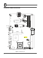

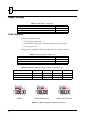
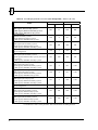

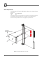


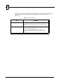


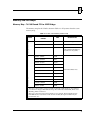

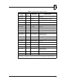
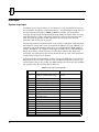
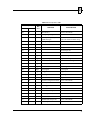


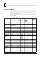
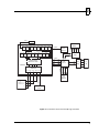


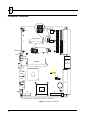


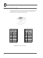
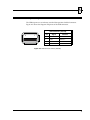


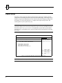
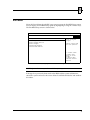


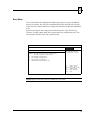

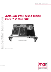
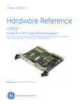
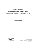

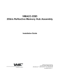

![[Insert the picture here]](http://vs1.manualzilla.com/store/data/005750886_1-61b7896b0a61bec1f004b64a994fc9d3-150x150.png)