1
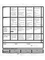
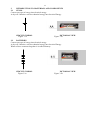
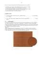
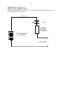
1 TECHNOLOGY ASSESSMENT TASK: CAPABILITY TASK : ”KEEPING IT CONNECTED” LEARNING OUTCOMES: LO 1. Technological processes and skills LO 2. Knowledge and understanding of electronic systems LO 3. Technology, society and the environment ASSESSMENT STANDARDS: 9.1.1.1 Identifies and explains a problem, need or opportunity from a given real-life context, and investigates the context, the nature of the need, the environmental situation, and the people concerned. 9.1.1.2 Analyses existing products relevant to an identified problem, need or opportunity based on: safety; suitability of materials; fitness for purpose; cost; manufacturing method. 9.1.1.3 Develops and performs practical testing procedures to determine or compare the suitability or fitness for purpose of relevant properties of materials, electrical or mechanical systems, structures, processes or finished products. 9.1.2.1 Writes or communicates a short and clear statement or a design brief for the development of a product or system related to a context, problem, need or opportunity that has been identified by self. 9.1.2.2 Lists product and design specifications and constraints for a solution to an identified problem, need or opportunity based on all of the design key words listed below:• people: age, target market, human rights, access; • purpose: function, what product will do;• appearance and aesthetics: form, colour, shape, feel;• environment: where product will be used or made, impact on the environment in the long and short term;• safety: for users and manufacturers;• cost: cost of materials, wastage, cost of manufacture, maximum selling price;• ergonomics;• quality;• production: mass production, batch production, one-off production. 9.1.2.3 Generates a range of possible solutions that are significantly different from each other, and that show clear links to the design brief and the specifications and constraints. 9.1.2.4 Chooses possible solutions based on well-reasoned argument related to the specifications and personal opinions, and develops a chosen idea using graphics. 9.1.3.1 Develops plans for making that include all of the following:• resource lists (e.g. materials lists, tools, people, costs);• formal drawing 9.1.3.2 Chooses and uses appropriate tools and materials to make designed products with precision and control by measuring, marking, cutting or separating, shaping or forming, joining or combining, and finishing a range of materials accurately and efficiently. showing dimensions or quantities (e.g. orthographic, oblique or isometric views, sequence drawings, exploded views);• manufacturing sequence (e.g. flow diagrams, flow charts). 9.1.3.3 Demonstrates knowledge and understanding of safe working practices and efficient use of materials and tools. 9.1.4.1 Evaluates the product or system based on self-generated objective criteria linked directly to the design brief, specifications and constraints using self-designed procedures (e.g. surveys, questionnaires, testing procedures) for self-testing, and suggests sensible improvements or modifications that would clearly result in a more effective or higher-quality end product. 9.1.5.1 Presents ideas (in a project portfolio) using formal drawing techniques, in two-dimensional or threedimensional sketches, circuit diagrams or systems diagrams that include all of the following features:• use of South African conventional drawing standards (e.g. scale, outlines, dimension lines, first and third angle projection);• notes that clarify design reasoning and key choices;• impressive enhancements of significant sketches (e.g. colour, texture, shade, thick and thin lines, shadow). 9.1.5.2 Chooses and uses appropriate technologies to combine and organise graphics and text effectively to produce project portfolios, poster presentations, case study reports, and so on, that have a formal organised structure appropriate for the target audience. 9.2.3.2 Demonstrates knowledge and understanding of how simple electronic circuits and devices are used to make an output respond to an input signal (e.g. resistors, light-emitting diodes, transistors, push or magnetic switches, thermistors, light-dependent resistors). 9.3.2.1 Recognises and identifies the impact of technological developments on the quality of people’s lives and on the environment in which they live, and suggests strategies for reducing any undesirable effects. 9.3.3.1 Produces evidence that details opinions, backed up by factual evidence, about bias (e.g. gender, age, access) in making technological decisions, and suggests strategies for redress. 2 FORM/S OF ASSESSMENT: Project KNOWLEDGE SKILLS VALUES * simple electronic circuits and devices, * outputs responding to an input signal (e.g. resistors, light-emitting diodes, transistors, push or magnetic switches, thermistors, light-dependent resistors). * Circuit and systems diagrams * Technological process skills: Investigate, design, make and evaluate * communicate using circuit and systems diagrams * Soldering * the impact of technological developments on the quality of people’s lives and on the environment in which they live * strategies for reducing any undesirable effects. * gender biase in technology DESIGN SITUATION / SCENARIO As a young person in today’s electronic age it is becoming important for people to identify components of electronic devices that are not working in an electronic / electrical system. During the resent power outages a number of electronic / electrical equipment in your house is no longer working. A Circuit Tester would be a useful device to have at home to do fault finding on electronic circuits. You will be issued with the electronic components to build a circuit for a circuit tester but a housing will be needed for the assembled device to make it functional and user friendly for boys and girls to use. THE ROLE OF THE TEACHER: Provide the electronic equipment. Provide opportunities for developing knowledge and skills when working with electronics INSTRUCTIONS FOR THE LEARNER: THE CAPABILITY TASK Complete the tasks as set out in the module Investigate various electronic devices and circuits Identify various electronic components and their symbols Read the resistance value on a resister Draw circuit diagrams Investigate the influence of different value resisters in a circuit Practice soldering skills Use a soldering iron to join electronic components Use a vero board to build a circuit tester / CONTINUITY TESTER Design and make your own innovative / creative housing for the electronic device Present a project portfolio that communicates all the technological step followed in designing the housing for the circuit tester. Use suitable communication skills to draw circuit diagrams of the various circuits in the portfolio OR A JOURNAL 3 RUBRIC/S / MEMO FOR THE ASSESSMENT TASK: NAME OF LEARNER: ________________________________ TECHNOLOGY CLASS:_9_ TITLE OF THE PROJECT: ___________” KEEPING IT CONNECTED”_________ (LO 1, 2 AND 3) FORM OF ASSESSMENT: PROJECT: DATE: _______________________ (SAASTE Rubric and changes by Alistair Mather) CRITERIA Investigates X3 Designs X4 Makes X3 Highly effective 5, 4 Highly developed in the skill of finding out things reflected by: * An ability to critically analyse situations, briefs, scenarios, etc. so as to identify possible problems, needs or opportunities and articulate this clearly. * An ability to access detailed information by using a range of skills like: analysing existing products, doing practical testing procedures and using suitable technologies to locate, collect, present and compare information. Highly developed in the skill of planning reflected by: * Ability to state intent explicitly (design brief) and further include quality parameters (specifications) * A good variety of detailed quality alternative solutions. * Well thought out and articulated reasons for choices made. * A detailed and appropriate development of chosen solution. Highly developed in the skill of Manufacturing reflected by: * Manufacturing accurately in line with the design (working drawing) * Made in accordance with the plan of action that was set out; *Any deviation is justified LEVELS OF PERFORMANCE Most areas are effective Some areas are effective 3 2 Not effective 1, 0 Good skills of finding out things reflected by: * An ability to analyse situations, briefs, scenarios, etc. so as to identify possible problems, needs or opportunities and state findings. Skills of finding out things are reflected by: * A basic ability to analyse situations, briefs, scenarios, etc. and a need to be prompted about possible problems, needs or opportunities. Very basic or lack of skills of finding Out things are reflected by: * An inability to analyse, that results in a constant need to be prompted about possible problems, needs or opportunities. * An ability to access information by using a range of skills like analysing existing products, doing practical testing procedures and using suitable technologies to locate, collect, present and compare information. Good skills of planning reflected by: * Ability to state intent (design brief) and further include parameters (specifications) * A good variety of alternative solutions. * Well thought out and articulated reasons for choices made. *An appropriate development of chosen solution * An ability to access information by using a some of the skills like analysing existing products, doing practical testing procedures and using suitable technologies to locate, collect, present and compare information. Skills of planning are reflected by: * A basic ability to state intent (design brief) and a need to be prompted on parameters (specifications) * Limited solutions (not always alternative). * Reasons for choices made not well thought out or non existent. * The chosen solution is not well developed. Skills of Manufacturing are reflected by: * A basic ability to manufacture in line with the design (working drawing) * Made but not always in accordance with a plan of action. * An inability to access information by using skills like analysing existing products, doing practical testing procedures and using suitable technologies to locate, collect, present and compare information. Very basic or lack of skills of planning are reflected by: * A constant need to be prompted to state intent (design brief) and parameters (specifications) * Little or no alternative solutions. * Absence of reasons for choices. * The chosen solution is not well developed. Good skills of Manufacturing reflected by: * Manufacturing in line with the design (working drawing) * Made in accordance with the plan of action that was set out. Score / 15 / 20 Very basic or lack of Skills of Manufacturing are reflected by: * Manufacturing that reflects little or no correlation to the design (working drawing) * Is made without a plan of action. / 15 4 Evaluates X2 Communicates X3 LO 2 Technological Knowledge and Understanding X3 LO 3 Technology Society and the Environment. X2 Highly developed in the skill of evaluating reflected by: * Logical thought- out evaluating based on detailed criteria. * Appropriate testing procedures carried out where necessary. * Explanations, justifications support findings throughout the process. Good skills of evaluating reflected by: * Well thought out evaluating based on criteria. * Appropriate testing procedures carried out where necessary. * Adequate explanations, justifications to support findings. Skills of evaluation are reflected by: * A basic ability to evaluate using criteria; sometimes evaluating without criteria. * Basic or inappropriate testing procedures. * Some or no explanations, justifications to support findings. Very basic or lack of evaluation skills of Reflection are reflected by: * Evaluation is not done or is inappropriate * No evidence of testing procedures. * The absence of any explanations or justifications Highly developed in the skill of Presentations reflected by: * An excellent understanding of graphical techniques. * The use of appropriate method/s of presentation. * Presentation of work is in a logical sequence. Good skills of Presentations reflected by: * A good understanding of graphical techniques. * The use of acceptable method/s of presentation. * Presentation of work is mostly in a logical sequence. Skills of Presentations are reflected by: * A basic understanding of graphical techniques. * Method/s of presentation are not always appropriate. * Presentation of work is not always in logical sequence. Very basic or lack of Skills of Presentations are reflected by: * Little or no understanding of graphical techniques. * Inappropriate method/s used in presentation. * Presentation of work is not in any logical sequence. Demonstrates an accurate understanding of and can apply appropriate knowledge accurately at a complex level. Demonstrates an accurate understanding and can apply appropriate knowledge accurately at the appropriate level. Demonstrates some understanding of and can apply knowledge partially at the appropriate level. Demonstrate little understanding of knowledge at a level lower than the appropriate level. / 10 / 15 / 15 Shows accurate evidence of having considered all the relevant factors that impact on the inter-relationship between Science, Technology, Society and the Environment at a complex level Shows accurate evidence of having considered relevant factors that mostly impact on the interrelationship between Science, Technology, Society and the Environment at an appropriate level. Shows some evidence of having considered factors that partially impact on the inter-relationship between Science, Technology, Society and the Environment at an appropriate level. Shows little evidence of having considered factors that impact on the inter-relationship between Science, Technology, Society and the Environment at a level lower than the appropriate level. COMMENT: LEARNER : _________________________ PARENT: ____________________________TEACHER: ________________________ Date: ___________________ SUMMARY CODE PER LEARNING OUTCOME: LO 1 LO 2 LO 3 CODE ACHEIVED LEARNER: _______________________ TEACHER___________________________ PARENT ________________________________ DATE _______________ _______________ / 10 /100 5 TECHNOLOGY ASSESSMENT TASK INDEX 1 DESCRIPTION PAGE No. OUTCOME 1 2. INTRODUCTION TO MATERIALS AND COMPONENTS 2.1 Cells 2 2.2 Batteries 2 2.3 Resistors 3 Assessment activity No.1 (colour code of resistors) 4 2.4 Switch 4 2.5 Basic Electric Circuit 5 Assessment activity No.2 (circuit construction) 5 2.6 Light emitting diode 6 2.7 A light emitting diode circuit 6 2.8 Veroboard 9 2.9 Plastic box 9 2.10 Soldering 10 Assessment activity No.3 (solder exercise) 11 3 CAPABILITY TASK Assessment activity No.4 (design and drawing) Assessment activity No.5 (design a pc-board layout) Assessment activity No.6 (preparation of veroboard) Assessment activity No.7 (assembly of veroboard) Assessment activity No.8 (soldering on veroboard) 3.1 Assemble the tester 3.1 Write a user manual for your tester 12 12 14 15 16 17 18 18 TECHNOLOGY ASSESSMENT TASK 1. OUTCOME: You will be able to: identify various electronic components and their symbols Read the resistance value on a resister Draw circuit diagrams Investigate the influence of different value resisters in a circuit Use a vero board to build a circuit Use a soldering iron to join electronic components Present a project portfolio which communicates the design process. To make a CONTINUITY TESTER Design and make a suitable housing for the circuit tester 2 6 2 INTRODUCTION TO MATERIALS AND COMPONENTS 2.1 CELLS: Convert one type of energy into electrical energy A dry cell / batteries: converts chemical energy into electrical Energy. CIRCUIT SYMBOL Figure 3.1a PICTORIAL VIEW Figure 3.1b 2.2 BATTERIES Convert one type of energy into electrical energy A dry cell / batteries: converts chemical energy into electrical Energy. When cells are connected together it is called a battery. CIRCUIT SYMBOL Figure 3.2a PICTORIAL VIEW Figure 3.2b 7 2.3 RESISTORS THE RESISTOR COLOUR- CODE CHART Figure 3.3 Value Colour 0 1 2 3 4 5 6 7 8 9 Black Brown Red Orange Yellow Green Blue Violet Grey White Silver Gold 1 st 2 nd Significant Significant Figure Figure 0 1 1 2 2 3 3 4 4 5 5 6 6 7 7 8 8 9 9 Multiplier Tolerance 10 1% 100 2% 1000 10000 100 000 1000 000 10 000 000 100 000 000 1000000000 10% 5% The E12 series is a typical example where there are only 12 values and multiples of those 12 values in the series: 10; 12; 15; 18; 22; 27; 33; 47; 56; 68; 74; 82 . With an accuracy/tolerance 20% this series will cover the full range of every possible value. ASSESSMENT ACTIVITY Nr.1 Complete the table below by establishing the resistance value with the aid of the colour code. No 1 2 3 4 Colour coded value of resistor Fist Second Third Colour colour Colour Red Red Red Brown Black Orange Yellow Vilot Yellow Green Blue Brown Fourth Colour Gold Silver Gold Gold Numeric value of resistor First Second Third Digit Digit Digit CRITERIA: 1 mark per correct answer 5 x 4 = 20 Percentace tolerance Total Value Assessment Mark allocation 8 2.4 SWITCH: In a Mechanical switch a force has to be applied to bring together or separate electrical conducting metal contacts. The following contact configurations are used as examples of poles (no of circuits) and throws (no of alternative connections) for Toggle switches. SPST: single pole single throw (single pole on-off) CIRCUIT SYMBOL Figure 3.4a PICTORIAL VIEW Figure 3.4b 9 2.5 BASIC ELECTRIC CIRCUIT: (understand concepts such as conductivity and insulation) An Electric circuit is a complete electrical path that will make it possible for an electric current (Amperes- denoted with the letter “I”). to flow from the positive terminal of a battery, through the conductors and components to the negative terminal. The battery supplies the force - electrical VOLTAGE and is denoted with the letter “V”. A basic electric circuit consist of die following: a Power supply - cell or battery (Energy source) Conductors - usually insulated Switch - when the switch is closed we have a completed circuit. A load eg. lamp, resistor, electric motor etc. RESISTOR POWER SOURCE = 9 V BATTERY SWITCH Figure 3.5 10 ASSESSMENT ACTIVITY Nr.2 Construct the basic electric circuit as per diagram above in Figure 3.5 STEPS 1. Connect the plus of the power supply (9 volt battery) to the one side of the switch 2. Connect the other side of the switch to the resistor (1000 ohm) 3. Connect the other side of the 1000 ohm resistor to the minus of the power supply (the - of the 9 volt battery) Assessment criteria: 1 mark per step correctly executed 3 x 1 = 3 Total … 2.6 LIGHT EMITTING DIODE A LED light emitting diode allows current flow through is in only one direction, from the anode to the cathode. The voltage – current characteristics of the LED is similar to that of the ordinary diode. LEDs are solid-state devices requiring little power and generating little heat. Because their heat generation is low and because they do not rely on a deteriorating material to generate light, LEDs have long operating lifetimes. Anode Cathode Fig 3.6 LIGHT EMITTING DIODE 2.7 A LIGHT EMITTING DIODE CIRCUIT Component list 1. Power supply - 9 volts battery 2. Led 3. Switch - spst 4. R1 = 2200 ohm resistor 5. R2 = 10 000 ohm resistor 6. R3 = 470 000 ohm resistor 7. R4 = 560 ohm resistor 8. Insulated conductors 11 Led CURRENT LIMITTING RESISTOR POWER SOURCE = 9 V BATTERY SWITCH Fig 3.7 Electric circuit with a LED (the resistor limits the current to protect the LED) STEPS 1. Connect the plus of the power supply to the Anode of the LED 2. Connect the Cathode of the LED to the one side of (R4) 560 ohm resistor 3. Connect the other side of (R4) 560 ohm resistor to the one side of the switch 4. Connect the minus of the power supply (the GND) to the other side of the switch 5. Turn ON the switch (The LED should be ON) 6. Now disconnect R4 and replace it with R1 What do you observe?………………... 7. Now disconnect R1 and replace it with R2 What do you observe?………………... 8. Now disconnect R2 and replace it with R3 What do you observe?………………... 9. Now disconnect R3 and replace again with R4 10. Turn the switch OFF Led CURRENT LIMITTING RESISTOR POWER SOURCE = 9 V BATTERY SWITCH 12 Fig 3.8 Electric circuit with a LED (LED connected in reverse mode) 11. Disconnect the Anode of the LED from the plus of the power supply 12. Disconnect the Cathode of the LED from the resistor R4 13. Now connect the Cathode of the LED to the plus of the power supply. 14. Now connect the Anode of the LED to the resistor R4 15. Turn ON the switch (The LED should be ……..) OBSERVATION : The LED conducts current when the (cathode/anode) …………………. is connected to the + voltage. The value of the resistor influence the current flow and thus the ……………….. of the LED . 2.8 VEROBOARD Veroboard or stripboard can be used to build useful and interesting projects. We are going to use a piece of (60 mm x 17 mm) on a 0.1 inch matrix - 22 holes by 6 copper (connecting) strips. The components are normally mounted between the strips. If your layout requires that a component must be mounted on a strip, a break must be introduced into the strip to prevent the component from being short circuited. Figure 3.9 When mounting a number of components on a board it is usually necessary to introduce breaks in the strips to prevent undesirable interconnections. The breaks in the copper strips (where applicable) are made with 3,0 mm twist drill held in the hand. 13 2.9 PLASTIC BOX (Make own container) Figure 3.10 Plastic box 85 x 55 x 30 mm 2.10 SOLDERING Soldering is the process of using a metallic alloy with a relative low melting point to unite conductors in electric circuits in order to ensure good conductivity. A good soldering joint must have a: Low resistance and be Mechanical strong (Solder is NOT intended as a kind of glue) PREPARING AND TINNING OF SOLDERING IRON BIT PREPARING AND SOLDERING OF JOINT The bit of the soldering iron must be cleaned and tinned at all times. Using a fine file, prepare the working face of the tip to a smooth and shiny surface. Heat up soldering iron until tip colour turns brownish. Touch resin-core (not acid-core) solder on tip and allow a little to melt, spread it over the surface quickly by rubbing briskly with a clean, dry rag. Melt a little more solder on face of tip and rub briskly until the tip has a uniform, bright, silvery colour. The iron is now tinned and ready for use. To preserve the tinning, the tip should be wiped frequently with a clean rag. Overheating will burn away the tinned surfaces. Clean both parts thoroughly and make a mechanical strong joint. (Do Not use Acid for cleaning) Heat up joint by pressing the hot tip of he soldering iron against the clean joint to be soldered. When the joint is hot, continue to hold the iron in contact with it and touch the tip of a piece of rosin-core solder to the joint. If the joint is hot enough, the solder will melt and flow like water into all the crevices of the joint and over it. Remove the iron and allow the joint to cool before disturbing it. 14 ASSESSMENT ACTIVITY NO.3 Design a simple object from the given piece (1 metre) of copper wire by bending the wire into an interesting shape. Your object must contain at least 5 solder joints. (A few ideas will be given by the educator.) SOLDERING LEVEL CRITERIA Joints enclosed in solder 1 Joints partly enclosed in blobs of solder 2 Joints partly enclosed in solder Bright solder joints Solder joints are ALL dull and uneven Some solder joints are bright and glossy Solder joints free from holes, pits and sharp protrusions Solder joints full of holes, pits and sharp protrusions Removal of flux No attempt was made to remove the flux Only some solder joints are free from holes, pits and sharp protrusions Some attempt was made to remove the flux 3 Joints entirely enclosed in solder, but all the contours of the junction is not exhibited Most of the solder joints are bright and glossy with a mirror like finish Most of the solder joints are free from holes, pits and sharp protrusions Most of the flux was removed 4 Joints entirely enclosed in solder, yet exhibiting all the contours of the junction Solder joints are ALL bright and glossy with a continuous mirror like finish Solder joints are ALL free from holes, pits and sharp protrusions All the flux was removed 15 3 CAPABILITY TASK THE DESIGN SITUATION: As a young person in today’s electronic age it is becoming important for people to identify components of electronic devices that are not working in an electronic / electrical system. During the resent power outages a number of electronic / electrical equipment in your house is no longer working. A Circuit Tester would be a useful device to have at home to do fault finding on electronic circuits. You will be issued with the electronic components to build a circuit for a circuit tester but a housing will be needed for the assembled device to make it functional and user friendly. COMPONENT LIST Item Description Quantity B1 9 Volt battery (pp6) with battery clip 1 R1 470 ohm resistors 1 D1 Red Led 5 mm 1.5 volts with mounting rings 1 PC 60 mm x 17 mm Copper clad Veroboard 0.1 matrix 1 TL Tests Lead with Crocodile clips 2 SPECIFICATIONS 1. All the components must be mounted inside a container 2. The test leads must protrude from one of the short sides of the container 3. The board must be exactly 60 mm x 17 mm (22 holes x 6 strips) 4. The board must contain at least one wire connection between copper strips 5. The board must have at least one break in a copper strip 6. All the terminating ends must be as close as possible to one of the short sides of the board. 7. All components must be laid out square and parallel to the sides of the board. 8. Polarity and identification marks must were applicable be indicated on the design 16 ASSESSMENT ACTIVITY: COMMUNICATION Nr.4 DESIGN LAYOUT OF PROJECT - (container) Draw the complete layout of the container to accommodate all components. DESIGN LAYOUT OF PROJECT - (container) LEVEL CRITERIA 1 2 3 Style of presentation A very low level of ability that is evident in: Work that is incomplete and does not show understanding of positioning views and/or aspects to be considered in presentations. A satisfactory level of ability that shows a limited understanding of: Positioning of views Aspects to be considered in presentations A high level of ability that shows understanding of: Acceptable positioning of views A limited range of considerations in presentations Presentation A very low level of skill evident in drawings that: Is incomplete and shows little attention to size, shape, accuracy A satisfactory level of skill evident in drawing that: almost fulfils the size and shape Use of correct/acceptab le conventions A very low level of knowledge & application of drawing conventions that is evident in: Incomplete work that shows little attention to the use of acceptable line types and the techniques of dimensioning, sectioning and naming, labelling. A level of knowledge & application of drawing conventions that is evident in most drawings in terms of the incorrect use of: Line types Dimensioning techniques Sectioning techniques A High level of skill evident in drawing that: Satisfies size and/or shape Show some deviations in accuracy A high level of knowledge & application of drawing conventions that is evident in some drawings in terms of the correct use of: Line types Dimensioning techniques Sectioning techniques 4 A very high level of ability that shows understanding of: Positioning of views The use of positive and negative space Aesthetic considerations in presentations A very high level of skill evident in drawing that: is perfect according to size & shape. A very high level of knowledge & application of drawing conventions that is evident in all drawings in terms of the consistent correct use of: Line types Dimensioning techniques Naming / Labelling techniques Sectioning techniques 17 ASSESSMENT ACTIVITY Nr.5 DESIGN OF PC-BOARD LAYOUT Design a VEROBOARD circuit layout for a CONTINUITY TESTER by making use of the circuit diagram below. Figure 3.11 Figure 3.11 Led CURRENT LIMITTING RESISTOR POWER SOURCE = 9 V BATTERY TEST LEADS 18 ASSESSMENT ACTIVITY Nr.6 PREPARATION OF THE VEROBOARD Square and finished off Veroboard to exactly 60 mm x 17 mm? Avoid touching board with your fingers as this makes it greasy. Break the copper strips (where applicable) with 3,0 mm twist drill held in the hand. Fit wire connection/s between copper strips. CHECKLIST PREPARATION OF THE VEROBOARD DESCRIPTION Veroboard finished off Square and exactly 60 mm x 17 mm? Complete break in copper strips (where applicable) with 3,0 mm twist drill held in the hand. No greasy. fingers prints on board Fit Wire connection/s between copper strips fitted correctly. SELF YES NO PEER YES NO 19 ASSESSMENT ACTIVITY Nr.7 ASSEMBLE PC BOARD CRITERIA components, fitted correctly Component leads bend at 90° to the correct spacing of veroboard Component fitted parallel or at 90° to a short side of the board LEVEL 2 3 Some of Most of the polarities and polarities and lead lead identification identification correct correct Component Some attempt Component leads not bend at made to get leads bend at 90°, and not to component 90° and to the the correct leads at 90°and correct spacing spacing of to the correct of veroboard veroboard spacing of veroboard Component Component Component fitted parallel fitted parallel to fitted parallel or randomly a long side of at 90° to a short the board side of the board 1 polarities and lead identification not considered 4 ALL polarities and lead identification taken into considerations Component leads bend accurately at 90° and to the correct spacing of veroboard Component fitted neatly, parallel or at 90° to a short side of the board Fit and solder all components, take care that the components are fitted correctly as far as polarities and lead identification is concerned. all components should be prepared by bending (at 90°) the leads to the correct spacing between holes on veroboard. SAFETY PRECAUTIONS WITH SEMICONDUCTORS Diodes and transistors can be damaged by the heat of soldering . When their pigtail leads must be soldered into a circuit, each lead should be grasped firmly with a longnose pliers. The pliers tips should be close to the body of the diode or transistor, the large metallic mass of the pliers serves to conduct heat away from the component, preventing its entry inside where it could do damage. Continue to hold the lead with the pliers until there is no doubt that the joint has cooled completely. 20 ASSESSMENT ACTIVITY Nr.8 SOLDERING OF COMPONENTS ON THE BOARD LEVEL CRITERIA 1 2 3 4 surface around the component leads Joints partly enclosed in blobs of solder Joints partly enclosed in solder Joints entirely enclosed in solder, but all the contours of the junction is not exhibited. Joints entirely enclosed in solder, yet exhibiting all the contours of the junction. Solder joint concave Solder joint convex Brightness and glossiness of joint Solder joints are dull and uneven Indication of movement of joint while cooling Some solder joints are concave Some solder joints are bright and glossy. Most of the solder joints concave Most of the solder joints are bright and glossy with a mirror-like finish. All solder joints concave around all conductors concave, bright and glossy and show a continuous mirror-like finish. Solder joints free from holes, pits and sharp protrusions Solder joints full of holes, pits and sharp protrusions Removal of flux No attempt was made to remove the Flux Only some solder joints are free from holes, pits and sharp protrusions Some attempt made to remove the flux Most of the solder joints are free from holes, pits and sharp protrusions Most of the flux removed Solder joints are ALL free from holes, pits and sharp protrusions All flux thoroughly removed 3.2.1 ASSEMBLE THE TESTER Measure, mark and drill all holes. Fit and solder all components, take care that the components are fitted correctly as far as polarities and lead identification is concerned. 3.2.2 WRITE A USER MANUAL FOR YOUR TESTER The visual outline of the tester indicating all the various terminals and indicators must be included in your user manual. ---------------------------------------------------------------------------------------------------------------PRESENT YOUR PROJECT PORTFOLO AND PRODUCT FOR ASSESSMENT Initial project by Jan Randewijk and adapted by Alistair Mather.