1
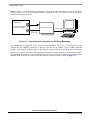
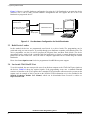
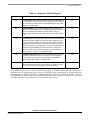
Freescale Semiconductor
Application Note
Production Flash
Programming
Techniques for Production Programming the
56F8300 and 56F8100 Families of Devices, Flash
Memory Blocks
AN1973
Rev. 1, 9/2005
Contents
1. Introduction .........................................1
2. Background Information .....................2
2.1 Considerations for Choosing a
Production Programming Method ...2
3. Programming Method Details .............3
Les Lewis
Note: All references to Data Flash in this document apply only
to the 56F8300 family of devices; the 56F8100 devices do not
support Data Flash.
3.1
3.2
3.3
3.4
3.5
Serial SCI Bootloader .....................3
Serial CAN Bootloader ................... 5
Bulk Device Loader ........................ 6
In-circuit JTAG/OnCE Port ............ 6
GPIO Flash Programming Mode .... 8
4. Conclusion ..........................................8
1.
Introduction
This document presents techniques and detailed information on
production programming of the Program, Data, and Boot Flash
memory blocks in the 56F8300 and the Program and Boot
Flash memory blocks in the 56F8100 components. This is
distinct from the developmental loading of the Flash blocks that
is achieved using developmental tools such as the Metrowerks
CodeWarrior for Freescale debugger.
There are four ways to program the Flash blocks in a factory
environment:
•
Using the Serial Bootloader present in the Boot Flash
•
Using a commercially-available device programmer
•
Using the JTAG/OnCETM port
•
Using GPIO pins with a custom bootloader
The first two methods do not require any developmental effort
to use. Using the JTAG/OnCE port currently requires the user
to develop his own loader program. Using the GPIO pins to
obtain the Flash programming data would also require the
customer to develop his own loader program.
© Freescale Semiconductor, Inc., 2005. All rights reserved.
5. References ...........................................8
Background Information
2.
Background Information
As a starting point, all methods require an application to be created using the CodeWarrior development tools.
This application must be specifically targeted to operate correctly from the internal Flash. The Freescale
CodeWarrior Development tools includes information as well as code to aid in the development of the
application. It is highly recommended that a developer start with the appropriate Processor Expert (PE)
stationery. This will greatly facilitate the development of the application, and includes all the elements required
to create embedded applications targeting internal Flash or external memory. During development and debug
of the application, the CodeWarrior tool can be used to program the internal Flash and to debug the program
while running from Flash. Once the development and test are complete, the CodeWarrior tool can also be used
to generate the source file containing the executable image of the Program, Data and Boot Flash blocks. In this
case, the source file is an S-record file. The S-record file contains the hex machine code and hex data
information formatted in a text file containing a series of S3-type S-records. Refer to Appendix A at the end
of this document for a detailed description of the format of the S-record file.
The CodeWarrior tool normally uses .elf files to store the application executable and to program the Flash
blocks in the devices. The user must specifically configure the CodeWarrior tool to create the S-record file.
Please refer to the CodeWarrior IDE Targeting DSP56800 Manual for information on how to turn on
S-record generation. The CodeWarrior tool generates three separate types of S-record files:
•
output_filename.p.S contains the Program and Boot Flash image
•
output_filename.x.S contains the Data Flash image
•
output_filename.S contains the combined Program, Boot and Data Flash images
The S-record file is the source file used by all the methods of production Flash programming. The file to use
when performing Flash programming will generally be the combined file, containing the Program, Boot, and
Data Flash image.
2.1 Considerations for Choosing a Production Programming Method
A fundamental decision to be made is whether to initially program the devices after they have been soldered to
the circuit board, or to initially program the devices before they are placed onto the circuit board. Programming
with the Boot Flash Serial Bootloader, programming via the JTAG/OnCE port and the GPIO Flash
programming mode are primarily intended as in-circuit programing methods. The bulk device load method is
an out-of-circuit programming method, which allows programming the 56F8300 and 56F8100 devices in
advance of the production run.
An additional consideration is which Flash blocks are to be programmed. The 56F8300 and 56F8100 products
do not allow for software to run from a Flash block that is concurrently being erased and programmed. Because
all 56F8300 products have multiple Program Flash blocks, this is not a significant restriction, but does require
advance planning with the set-up of the Flash programming algorithms. For example, the Serial Bootloader is
programmed into the Boot Flash at the factory, and allows only for the programming of the Program and Data
Flash blocks because it restricts itself to only taking space in the Boot Flash. Therefore, it always runs from
Boot Flash and cannot reprogram any portion of the Boot Flash block. The Serial Bootloader can be used to
load all Flash blocks by implementing custom loader software that is loaded into the Program Flash, then used
to program the Boot Flash. By switching back and forth, all combinations of Flash programming can be
implemented. The Freescale Processor Expert for the 56F8300 and 56F8100 devices includes all software
components needed to write such an application.
Production Flash Programming, Rev. 1
2
Freescale Semiconductor
Serial SCI Bootloader
Since the JTAG/OnCE port and the bulk device loader mode options do not require that software be run from
any of the Flash blocks, they can reprogram any block without special considerations. The 56F8300 and
56F8100 chips are fully field reprogrammable, requiring no special voltages or external hardware to perform
this function. The stock Serial Bootloader fully supports field upgrades.
There is another option to consider. All of the 56F8300 and 56F8100 devices also contain on-chip program
RAM. A bootloader can be loaded into this RAM and, from there, all Flash blocks can be reprogrammed.
All in-circuit Flash loading methods require that the target hardware conforms to certain minimal standards.
For the Serial Bootloader, these standards require that:
•
The SCI port must be accessible for serial communications
•
To enable proper SCI communications, the external clock for the components must be set to the
recommended frequency. 8MHz is recommended for 56F8300 amd 56F8100 components.
Although the known external clock frequencies are necessary to ensure proper SCI communications, it’s
possible to drive the clock inputs during Serial Bootloading, then run the normal program at a different clock
frequency. In general, this will not be necessary, since in all likelihood the best choice for the external
operating frequency for the target circuit board will be the same frequency required by the Serial Bootloader.
Using the JTAG/OnCE port method requires only that a subset of the JTAG/OnCE pins be made available.
Please refer to Section 3.4 for details.
Using the GPIO port method would require access to any user-specified GPIO pins that the user-defined
bootloader software specified.
The approximate speeds at which the Flash blocks can be programmed with the various methods are:
3.
•
SCI Serial Bootloader version 1.01 = 2495 words per second
•
CAN Serial Bootloader version 1.01 = 3706 words per second
•
Bulk device programmer = 800 words per second
•
In-circuit JTAG/OnCE port = 800 words per second (using a parallel port command converter).
Programming Method Details
3.1 Serial SCI Bootloader
The software and protocol for this loader and how to use it are fully described in the Metrowerks on-line help
and web site (see References). Please refer to the SCI Bootloader application information in the 56F83xx
SCI/CAN Bootloader User Manual for the processor being used. This manual has detailed information on
how to use the Serial Bootloader and how to prepare your application for loading using the Serial Bootloader.
Table 3-1. Details of SCI Serial Bootloader Versions 1.01
Version
Baud Rate
Flow Control
Word Format
1.01
115,200bps
Xon/Xoff
8 data bits, no parity, 1 stop bit
Production Flash Programming, Rev. 1
Freescale Semiconductor
3
Programming Method Details
Figure 3-1 shows a possible hardware configuration for using the Serial Bootloader to program the device
in-circuit. This is one of many possible hardware configurations that will support the use of the Serial
Bootloader to program the device.
56F8300 Target
Hardware Card
Pads tied to SCI signal
lines TXD0 and RXD0
RS-232 Interface Card
RS-232 Cable
Two-pin probe
IBM-Compatible
Figure 3-1. One Hardware Configuration for SCI Serial Bootloader
The configuration in Figure 3-1 shows how the Serial Bootloader can be used, even though the target
hardware has no additional connectors or RS-232 serial drivers. In addition, using an IBM-compatible
computer is not required--any host capable of providing the required serial stream and the protocol can be used.
In general, it’s easiest to use the Serial Bootloader program by leaving it in place in the Boot Flash without
reprogramming the Boot Flash. The Serial Bootloader can be used effectively for field upgrades to the Program
and Data Flash. It can also be used to replace the firmware in the Boot Flash, as shown in Figure 3-2.
Production Flash Programming, Rev. 1
4
Freescale Semiconductor
Serial CAN Bootloader
Boot Flash
Serial Bootloader
runs and
downloads user
application into
Program and Data
Flash
Program Flash
Serial Bootloader transfers control to user application
User application
downloads
software and loads
it into the Boot and
Data Flash
Optionally, user's
loader software
runs and
downloads
additional software
into Program and
Data Flash
Control transferred to user software's Boot Flash software
Figure 3-2. Using the SCI Serial Bootloader to Program Boot Flash
3.2 Serial CAN Bootloader
The software and protocol for this loader and how to use it are fully described in the Metrowerks on-line help
and web site (see References). Please refer to the CAN Bootloader application information in the 56F83xx
SCI/CAN Bootloader User Manual for the processor being used. This manual has detailed information on
how to use the Serial Bootloader and how to prepare your application for loading using the Serial Bootloader.
The CAN Bootloader application is not present in the Boot Flash when the device is received from the factory.
If the CAN Bootloader is to be used, it must first be programmed into the Boot Flash in a manner similar to that
described in Figure 3-2.
Table 3-2. Details of CAN Serial Bootloader Versions 1.01
Version
Baud Rate
1.01
500,000bps
Production Flash Programming, Rev. 1
Freescale Semiconductor
5
Programming Method Details
Figure 3-3 shows a possible hardware configuration for using the CAN Bootloader to program the device
in-circuit. This is one of many possible hardware configurations that will support the use of the CAN
Bootloader to program the device.
56F8300 Target
Hardware Card
Pads tied to CAN signal lines
CAN_TX and CAN_RX
CAN Interface Card
Parallel Cable
Two-pin probe
IBM-Compatible
Figure 3-3. One Hardware Configuration for Serial Bootloader
3.3 Bulk Device Loader
In this method, the devices are programmed out-of-circuit in a device loader. The programming can be
performed using your own resources, or possibly through your distributor or another value-added reseller. The
device programmer can also be used to program the Program, Data, and Boot Flash blocks. The device
programmer can be used to load a complete and final application, or simply a custom Bootloader program
placed into the Boot Flash area. Later, the final or complete application can be loaded using the custom
Bootloader.
Please check www.bpmicro.com for device programmers from BP Microsystems support.
3.4 In-circuit JTAG/OnCE Port
To use this method, the user must provide access from his host computer to the JTAG/OnCE port signals on
the devices. Table 3-3 shows the required signals. If the programming set-up uses a standard command
converter to interface to the JTAG signals, then a standard JTAG pin header connector must be present on the
custom card. An example of this is present on the 56F8346 EVM; information on it is also included in the
56F8346 Evaluation Module User Manual, which can be downloaded from Freescale’s website at:
http://freescale.com.
Production Flash Programming, Rev. 1
6
Freescale Semiconductor
In-circuit JTAG/OnCE Port
Table 3-3. Required JTAG/OnCE Signals
Signal
Signal Description
Required
TDI
Test Data Input—This input pin provides a serial input data stream to
the TAP and the TLM. It is sampled on the rising edge of TCK. TDI has
an on-chip pull-up resistor which can be disabled through SIM_PUDR
register in the SIM module.
Yes
TDO
Test Data Output—This tri-state output pin provides a serial output
data stream from the Master TAP, or 56800E core TAP Controller. It is
driven in the Shift-IR and Shift-DR controller states of the TAP
Controller state machines. Output data changes on the falling edge of
TCK.
Yes
TCK
Test Clock Input—This input pin provides the clock to synchronize the
test logic and shift serial data to and from all TAP Controllers and the
TLM. If the EOnCE module is not being accessed using the Master or
56800E core TAP Controllers, the maximum TCK frequency is 1/4 the
maximum frequency for the 56800E core. When accessing the EOnCE
module through the 56800E core TAP Controller, the maximum frequency for TCK is 1/8 the maximum frequency for the 56800E core.
The TCK pin has a pull down non-disabled resistor.
Yes
TMS
Test Mode Select Input—This input pin is used to sequence the TAP
Controller’s TLM state machine. It is sampled on the rising edge of
TCK. TMS has an on-chip pull-up resistor which can be disabled
through SIM_PUDR register in the SIM module.
Yes
TRST
Test Reset—This input pin provides an asynchronous reset signal to
the TLM and all TAP Controllers. If the JTAG is not going to be used,
prevent signal interference by holding it low during operation.
Yes
The CodeWarrior tool can be used to download the program. A Windows application with source code to
demonstrate how to program the devices over the JTAG/OnCE port is documented in the application note,
“Programming On-Chip Flash Memories of DSP56F80x DSPs using the JTAG/OnCE Interface”, AN1935.
This application is available in the FAQs. Detailed information on how to program using the JTAG/OnCE port
is available and can be requested from your Freescale sales representative.
Production Flash Programming, Rev. 1
Freescale Semiconductor
7
Conclusion
3.5 GPIO Flash Programming Mode
This mode requires the customer to define his own definition of GPIO Flash programming pin definitions and
code load protocol. He would then have to develop an appropriate bootload application to program into the
Boot Flash. This approach would also require the customer to provide access to the required pins for his
program loading.
4.
Conclusion
The 56F8300 and 56F8100 components are very flexible in programming Flash blocks. In this application
note, several methods have been presented for programming the Flash blocks in a production environment.
One of these methods, or a variation of it, should meet your production Flash programming requirements.
5.
References
The following materials were used to produce this paper:
1. CodeWarrior IDE Targeting 56F8300 Manual
CodeWarrior for Freescale DSP56800E Embedded Systems, CWDSP56800E
2. Targeting Freescale 56F8300 Platform, Processor Expert
CodeWarriorTM Development Studio for 56800/E Hybrid Controllers with Processor Expert, CW568x
3. 56F83xx Evaluation Module Hardware User Manual for the device being implemented
4. 5683xx SCI/CAN Bootloader User Manual, MC56F83xxBLUM
5. Programming On-Chip Flash Memories of DSP56F80x DSPs using the JTAG/OnCE Interface, AN1935
6. Metrowerks help:
www.metrowerks.com/MW/support
or
[email protected]
Production Flash Programming, Rev. 1
8
Freescale Semiconductor
GPIO Flash Programming Mode
Appendix A
S-Record Specification
Note: All references to Data Flash in the appendix apply only to the 56F8300 family of devices; the 56F8100
devices do not support Data Flash.
1) Use only S0, S3 and S7 records
2) Three S-Record files are built with every compile. The first contains the contents of all initialized
PROGRAM (P) Memory contents. The second file contains the contents of all initialized DATA (X) Memory
contents.
3) The third S-Record file (the “combined” file) is roughly a concatenation of the P file with the X file (P
followed by X). The S3 data records targeted for X shall have an offset of 0x02000000 added to their byte
address fields. There shall be only a single pair of S0 and S7 records for the entire combined file.
Notes:
•
The P (and combined) file may contain: Program Flash contents, Program RAM contents, Boot Flash
contents
•
The X (and combined) file may contain: Data Flash contents, Data Ram contents
•
The device programming algorithm shall be address range aware
a) The byte address fields of S3 data records are examined by the device programming algorithm to
determine which Flash memory to access
b) The offset of 0x02000000 for X data records is required because the P and X memories within the
56F8300 devices both start at address 0. (S-Records don't normally support overlapping memories;
defining an offset is the most expedient work-around for the problem.)
c) Data specified for RAM locations shall be ignored by the device programming algorithm.
4) Unique codes shall reside in the P, X and combined S0 header records. In this manner, the S0 records will
identify the subsequent contents as either P, or X, or combined. The proposed S0 header records are as follows:
Code Example A-1. S0 Record for the P File
S0 0C 00000000 50 52 4F 47 52 41 4D DB
(Hex ASCII for: P R O G R A M )
Code Example A-2. S0 Record for the X File
S0 09 00000000 44 41 54 41 DC
(Hex ASCII for: D A T A )
Production Flash Programming, Rev. 1
Freescale Semiconductor
9
References
Code Example A-3. S0 Record for the Combined File
S0 11 00000000 50 52 4F 47 52 41 4D 26 44 41 54 41 96
(Hex ASCII for: P R O G R A M & D A T A)
Notes:
The device programming algorithm will not be expected to recognize contents within any S0 record.
The S0 content is only to aid with human recognition of file contents and to assist in content
recognition by future tools.
5) S3 data shall not split across a processor word size (16 bits). In other words, there shall be an even number
of “data” bytes within each S3 record.
Sample S-Record files for the 56F8300 and 56F8100 follow. (Spaces have been inserted for improved
readability in this document; “CS” is a space holder for the checksum byte.) The address fields of the S3 record
shall be conventional BYTE addresses and byte data shall be represented in the Little-endian format. (The
Least Significant Byte [LSB] is located at the lowest address.)
Notes:
•
In this manner, the constituent P or X S-Record files can be used to program any conventional
(external) non-volatile memory devices, without the need for any additional S-Record manipulation
utility programs
•
56F8300 and 56F8100 processors have a native 16 bit word. Likewise, the Flash memories are
programmed with 16-bit words and all addresses are interpreted as word addresses
•
To get from the S-Record Byte address to the 56F8300 and 56F8100 16-bit Word address, divide the
S-Record address field value by 2. For X memory, first subtract the 0x02000000 offset, then
unscramble the little-endian format to recognize the data words.
Code Example A-4. Sample P File
S0 0C 00000000 50 52 4F 47 52 41 4D DB
"PROGRAM"
S3 0D 00000000 10 32 11 32 12 32 13 32 CS
S3 0D 00000008 14 32 15 32 16 32 17 32 CS
S3 0D 00000010 18 32 19 32 1A 32 1B 32 CS
S3 0D 00040000 10 B2 11 B2 12 B2 13 B2 CS
S3 0D 00040008 14 B2 15 B2 16 B2 17 B2 CS
S7 05 00000000 CS
Boot Flash starts at word
address 20000
(byte address 40000)
Production Flash Programming, Rev. 1
10
Freescale Semiconductor
GPIO Flash Programming Mode
Code Example A-5. Sample X File
S0 09 00000000 44 41 54 41 DC
S3 0D 00002000 10 A2 11 A2 12 A2 13 A2 CS
S3 0D 00002008 14 A2 15 A2 16 A2 17 A2 CS
S7 05 00000000 CS
"DATA"
Note: There is no offset
used in the stand-alone
X S-Record file.
In this example, word
address 1000 is the first
location to be programmed.
Code Example A-6. Sample Combined File
S0 11 00000000 50 52 4F 47 52 41 4D 26 44 41 54 41 96
S3 0D 00000000 10 32 11 32 12 32 13 32 CS
"PROGRAM
& DATA"
S3 0D 00000008 14 32 15 32 16 32 17 32 CS
S3 0D 00000010 18 32 19 32 1A 32 1B 32 CS
S3 0D 00040000 10 B2 11 B2 12 B2 13 B2 CS
S3 0D 00040008 14 B2 15 B2 16 B2 17 B2 CS
S3 0D 02002000 10 A2 11 A2 12 A2 13 A2 CS
S3 0D 02002008 14 A2 15 A2 16 A2 17 A2 CS
Boot Flash starts at word
address 20000
Big offset of 0x02000000
signifies X data follows
S7 05 00000000 CS
S-Record Explanation
S0 05 00000000 (data) CS
S0
S3
S7
S0 is a header record
S3 is data
S7 terminator for block of S3
05
(hex) 5 bytes follow
00000000
32 bits of byte addresses
CS
The Least Significant Byte (LSB) of the one's
complement of the sum of the values represented
in the pairs of characters making up the record
length, address, and the data fields
Production Flash Programming, Rev. 1
Freescale Semiconductor
11
References
After programming the 56F8300 or 56F8100 with either the combined file or both stand-alone P and X files, a
debugger dump would yield results like those in the following Code Examples:
Code Example A-7. Dump of Program (P) Flash
address p:00 0000 = 3210
address p:00 0001 = 3211
address p:00 0002 = 3212
address p:00 0003 = 3213
address p:00 0004 = 3214...
Code Example A-8. Dump of Boot Flash
address p:02 0000 = B210
address p:02 0001 = B211
address p:02 0002 = B212
address p:02 0003 = B213...
Code Example A-9. Dump of Data (X) Flash
address x:00 1000 = A210
address x:00 1001 = A211
address x:00 1002 = A212
address x:00 1003 = A213
address x:00 1004 = A214...
Production Flash Programming, Rev. 1
12
Freescale Semiconductor
GPIO Flash Programming Mode
Production Flash Programming, Rev. 1
Freescale Semiconductor
13
References
Production Flash Programming, Rev. 1
14
Freescale Semiconductor
GPIO Flash Programming Mode
Production Flash Programming, Rev. 1
Freescale Semiconductor
15
How to Reach Us:
Home Page:
www.freescale.com
E-mail:
[email protected]
USA/Europe or Locations Not Listed:
Freescale Semiconductor
Technical Information Center, CH370
1300 N. Alma School Road
Chandler, Arizona 85224
+1-800-521-6274 or +1-480-768-2130
[email protected]
Europe, Middle East, and Africa:
Freescale Halbleiter Deutschland GmbH
Technical Information Center
Schatzbogen 7
81829 Muenchen, Germany
+44 1296 380 456 (English)
+46 8 52200080 (English)
+49 89 92103 559 (German)
+33 1 69 35 48 48 (French)
[email protected]
Japan:
Freescale Semiconductor Japan Ltd.
Headquarters
ARCO Tower 15F
1-8-1, Shimo-Meguro, Meguro-ku,
Tokyo 153-0064, Japan
0120 191014 or +81 3 5437 9125
[email protected]
Asia/Pacific:
Freescale Semiconductor Hong Kong Ltd.
Technical Information Center
2 Dai King Street
Tai Po Industrial Estate
Tai Po, N.T., Hong Kong
+800 2666 8080
[email protected]
For Literature Requests Only:
Freescale Semiconductor Literature Distribution Center
P.O. Box 5405
Denver, Colorado 80217
1-800-441-2447 or 303-675-2140
Fax: 303-675-2150
[email protected]
Information in this document is provided solely to enable system and
software implementers to use Freescale Semiconductor products. There are
no express or implied copyright licenses granted hereunder to design or
fabricate any integrated circuits or integrated circuits based on the
information in this document.
Freescale Semiconductor reserves the right to make changes without further
notice to any products herein. Freescale Semiconductor makes no warranty,
representation or guarantee regarding the suitability of its products for any
particular purpose, nor does Freescale Semiconductor assume any liability
arising out of the application or use of any product or circuit, and specifically
disclaims any and all liability, including without limitation consequential or
incidental damages. “Typical” parameters that may be provided in Freescale
Semiconductor data sheets and/or specifications can and do vary in different
applications and actual performance may vary over time. All operating
parameters, including “Typicals”, must be validated for each customer
application by customer’s technical experts. Freescale Semiconductor does
not convey any license under its patent rights nor the rights of others.
Freescale Semiconductor products are not designed, intended, or authorized
for use as components in systems intended for surgical implant into the body,
or other applications intended to support or sustain life, or for any other
application in which the failure of the Freescale Semiconductor product could
create a situation where personal injury or death may occur. Should Buyer
purchase or use Freescale Semiconductor products for any such unintended
or unauthorized application, Buyer shall indemnify and hold Freescale
Semiconductor and its officers, employees, subsidiaries, affiliates, and
distributors harmless against all claims, costs, damages, and expenses, and
reasonable attorney fees arising out of, directly or indirectly, any claim of
personal injury or death associated with such unintended or unauthorized
use, even if such claim alleges that Freescale Semiconductor was negligent
regarding the design or manufacture of the part.
Freescale™ and the Freescale logo are trademarks of Freescale Semiconductor,
Inc. All other product or service names are the property of their respective owners.
This product incorporates SuperFlash® technology licensed from SST.
© Freescale Semiconductor, Inc. 2005. All rights reserved.
AN1973
Rev. 1
9/2005