1
致尊敬的顾客
关于产品目录等资料中的旧公司名称
NEC电子公司与株式会社瑞萨科技于2010年4月1日进行业务整合(合并),整合后的
新公司暨“瑞萨电子公司”继承两家公司的所有业务。因此,本资料中虽还保留有旧公司
名称等标识,但是并不妨碍本资料的有效性,敬请谅解。
瑞萨电子公司网址:http://www.renesas.com
2010年4月1日
瑞萨电子公司
【发行】瑞萨电子公司(http://www.renesas.com)
【业务咨询】http://www.renesas.com/inquiry
Notice
1.
2.
3.
4.
5.
6.
7.
All information included in this document is current as of the date this document is issued. Such information, however, is
subject to change without any prior notice. Before purchasing or using any Renesas Electronics products listed herein, please
confirm the latest product information with a Renesas Electronics sales office. Also, please pay regular and careful attention to
additional and different information to be disclosed by Renesas Electronics such as that disclosed through our website.
Renesas Electronics does not assume any liability for infringement of patents, copyrights, or other intellectual property rights
of third parties by or arising from the use of Renesas Electronics products or technical information described in this document.
No license, express, implied or otherwise, is granted hereby under any patents, copyrights or other intellectual property rights
of Renesas Electronics or others.
You should not alter, modify, copy, or otherwise misappropriate any Renesas Electronics product, whether in whole or in part.
Descriptions of circuits, software and other related information in this document are provided only to illustrate the operation of
semiconductor products and application examples. You are fully responsible for the incorporation of these circuits, software,
and information in the design of your equipment. Renesas Electronics assumes no responsibility for any losses incurred by
you or third parties arising from the use of these circuits, software, or information.
When exporting the products or technology described in this document, you should comply with the applicable export control
laws and regulations and follow the procedures required by such laws and regulations. You should not use Renesas
Electronics products or the technology described in this document for any purpose relating to military applications or use by
the military, including but not limited to the development of weapons of mass destruction. Renesas Electronics products and
technology may not be used for or incorporated into any products or systems whose manufacture, use, or sale is prohibited
under any applicable domestic or foreign laws or regulations.
Renesas Electronics has used reasonable care in preparing the information included in this document, but Renesas Electronics
does not warrant that such information is error free. Renesas Electronics assumes no liability whatsoever for any damages
incurred by you resulting from errors in or omissions from the information included herein.
Renesas Electronics products are classified according to the following three quality grades: “Standard”, “High Quality”, and
“Specific”. The recommended applications for each Renesas Electronics product depends on the product’s quality grade, as
indicated below. You must check the quality grade of each Renesas Electronics product before using it in a particular
application. You may not use any Renesas Electronics product for any application categorized as “Specific” without the prior
written consent of Renesas Electronics. Further, you may not use any Renesas Electronics product for any application for
which it is not intended without the prior written consent of Renesas Electronics. Renesas Electronics shall not be in any way
liable for any damages or losses incurred by you or third parties arising from the use of any Renesas Electronics product for an
application categorized as “Specific” or for which the product is not intended where you have failed to obtain the prior written
consent of Renesas Electronics. The quality grade of each Renesas Electronics product is “Standard” unless otherwise
expressly specified in a Renesas Electronics data sheets or data books, etc.
“Standard”:
8.
9.
10.
11.
12.
Computers; office equipment; communications equipment; test and measurement equipment; audio and visual
equipment; home electronic appliances; machine tools; personal electronic equipment; and industrial robots.
“High Quality”: Transportation equipment (automobiles, trains, ships, etc.); traffic control systems; anti-disaster systems; anticrime systems; safety equipment; and medical equipment not specifically designed for life support.
“Specific”:
Aircraft; aerospace equipment; submersible repeaters; nuclear reactor control systems; medical equipment or
systems for life support (e.g. artificial life support devices or systems), surgical implantations, or healthcare
intervention (e.g. excision, etc.), and any other applications or purposes that pose a direct threat to human life.
You should use the Renesas Electronics products described in this document within the range specified by Renesas Electronics,
especially with respect to the maximum rating, operating supply voltage range, movement power voltage range, heat radiation
characteristics, installation and other product characteristics. Renesas Electronics shall have no liability for malfunctions or
damages arising out of the use of Renesas Electronics products beyond such specified ranges.
Although Renesas Electronics endeavors to improve the quality and reliability of its products, semiconductor products have
specific characteristics such as the occurrence of failure at a certain rate and malfunctions under certain use conditions. Further,
Renesas Electronics products are not subject to radiation resistance design. Please be sure to implement safety measures to
guard them against the possibility of physical injury, and injury or damage caused by fire in the event of the failure of a
Renesas Electronics product, such as safety design for hardware and software including but not limited to redundancy, fire
control and malfunction prevention, appropriate treatment for aging degradation or any other appropriate measures. Because
the evaluation of microcomputer software alone is very difficult, please evaluate the safety of the final products or system
manufactured by you.
Please contact a Renesas Electronics sales office for details as to environmental matters such as the environmental
compatibility of each Renesas Electronics product. Please use Renesas Electronics products in compliance with all applicable
laws and regulations that regulate the inclusion or use of controlled substances, including without limitation, the EU RoHS
Directive. Renesas Electronics assumes no liability for damages or losses occurring as a result of your noncompliance with
applicable laws and regulations.
This document may not be reproduced or duplicated, in any form, in whole or in part, without prior written consent of Renesas
Electronics.
Please contact a Renesas Electronics sales office if you have any questions regarding the information contained in this
document or Renesas Electronics products, or if you have any other inquiries.
(Note 1) “Renesas Electronics” as used in this document means Renesas Electronics Corporation and also includes its majorityowned subsidiaries.
(Note 2) “Renesas Electronics product(s)” means any product developed or manufactured by or for Renesas Electronics.
R8C/11 Group
E-Bike Reference Platform
E-Bike Reference
Platform
( R8C/11)
User’s Manual
RS-SZ
1st Edition
Published by: Renesas System Solutions (Beijing) Co., Ltd., Shenzhen Branch
Date: September 30, 2007 Version 1.00
. 2007 Renesas System Solutions (Beijing) Co., Ltd., Shenzhen Branch, All rights reserved.
RSSZEUM0001 – 0100
Rev.1.00
1
R8C/11 Group
E-Bike Reference Platform
About this manual
This user’s manual is written for Renesas E-bike Reference Platform.It
describes the hardware and software specifications of this platform.Pleas use
this user’s manual to understand the hardware and how to design R8C/11 for
the E-bike application.
The platform controls a Brushless motor with hall sensor by 120-degree
trapezoidal wave commutation.
Section 1 Overview and Features
Give an introduction to the hardware and software specifications of the platform.
Section 2 System Requirements
Introduce the requirements of the system.
Section 3 Block Diagram
Give an overview on the functional modules of the platform.
Section 4 Schematic Diagram
Give a description of each circuits or modules schematically and functionally.
Section 5 Control of E-bike Brushless DC Motor
Give a detail of E-bike Motor control system
Section6 Bill of Components
Give a detailed list of the components included in the system.
Section 7 Sample Software Flowchart
Give the detailed Sample Software flowchart description for the power meter application.
Section8 Using E8 Emulator for Debugging
Demonstrate how to debug in HEW environment by using E8 emulator.
RSSZEUM0001 – 0100
Rev.1.00
2
R8C/11 Group
E-Bike Reference Platform
1. Overview & Features
The R8C/11 E-bike solution is used to promote R8C/11 for the brushless DC motor with hall
Sensor E-bike application. Emulator E8 is used for software development. The demonstration
package should be given to customers with a demonstration board, a reference manual and a
software package.
Hardware Specification:
- High speed onchip oscillator(8 MHZ)
- DC 36V input for DC5V,12V regulation
- Six MOSFETS and MOSFET driver circuitry
- Current detect circuitry
- Voltage detect circuitry
- Short protect circuitry
- Hall sensor detect circuitry
- One LED
Software Specification:
- 120 degree Trapezoidal Wave Commutation
- Motor speed control function
- Commutation current control function
- MOSFET protection function
- Voltage protection function
- Uart communications
Reference Manual Specification:
- Demonstration board schematic
- Description of each hardware functions
- Material list
- Description of each software module in the software package
2. System Requirements
- 36V DC power supply
- Emulator, E8
- HEW installed in PC
- Compiler Package,NC30WA V.5.40
RSSZEUM0001 – 0100
Rev.1.00
3
R8C/11 Group
E-Bike Reference Platform
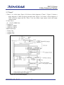
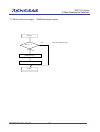
3. Block Diagram
The following diagram describes the system blocks and the figure shows the system
components, they help you have a general concept of this application.
LED Display
LED Display
I/O
Brake
Brake
I/O
Hall adjust speed
Hall adjust speed
A/D
MOSFET
MOSFET
5V
Voltage Conversion
Voltage Conversion
RSSZEUM0001 – 0100
Rev.1.00
BLDC with 120 degree
BLDC with 120 degree
R5F2114FP
Use onchip
oscilator(8MHZ)
4
6ch
PWM
MOSFET Driver
MOSFET Driver
A/D
MOSFET Current Sensor
MOSFET Current Sensor
INT
Motor Hall Sensor
Motor Hall Sensor
A/D
Voltage Sensor
Voltage Sensor
R8C/11 Group
E-Bike Reference Platform
4. Schematic Diagram
4.1 Voltage Regulating Circuit.
D8
R75
4007
VR1
R78
C29
330/2W
+12V
Vadj
VCC36V
C31
103
47uF/63V
Vin
Vout
GND
LM317
R80
R81
103
102
VR2
C34
470uF/25V
D9
D Zener
751
Vin
Vout
GND
78L05
VCC
C30
C32
D10
470uF/16V 104
D Zener
The Voltage regulating circuit change battery voltage 36v into 12V and 5V , It use of 12V for Mosfet driver ,
5V for MCU and other circuits.
4.2 Current Detection Circuit.
R3
VCC
sample
Res2
223
R10
R9
Res2
512
U2A
LM324AD
R18
4
VCC
Res2
473
1
A
11
2
3
Res2
102
to mcu
RSSZEUM0001 – 0100
Rev.1.00
5
R8C/11 Group
E-Bike Reference Platform
4.3 Short Circuit Detection Circuit.
VCC
R12
Res2
104 R8
Res2
472
sample
R16
Res2
103 C5
6
5
U2B
LM324AD
4
VCC
7
B
11
103
to mcu
4.4 Speedhandle Signal Detection Circuit.
J1
to speed-limit jumper
sl
J2
R25
to speedhandle
sp
RSSZEUM0001 – 0100
Rev.1.00
R27
103
R22
562
to mcu
202
C9
103
6
R8C/11 Group
E-Bike Reference Platform
4.5 Brakehandle Signal Detection Circuit.
C19
103
R59
472
R63
1
332
D7
4148
R66
153
to brake-handle(low in effect)
bk-l
J12
to brake-handle(high in effect)
bk-h
RSSZEUM0001 – 0100
Rev.1.00
R70
153
7
R67
472
3
J9
Q19
B5551
2
C
E
VCC
to mcu
C22
103
R8C/11 Group
E-Bike Reference Platform
4.6 Motor Driver Circuit.
D1
+12V
R1
1N4007
Res2
511
R14
103
R17
272
C7
222
3
4
5
Q2
5551
Res2
222
C2
R19
R26
272
9
10
C10 11
222
R23
Res2
222
to motor
D3
Q5
MOSFET-N
C6
Cap Pol1
100pF
C8
Q9
5401
8
R21
Res2
222
D4
4148
R20
Res2
511
Q11
5551
Res2
222
1
G
Q10
MOSFET-N
R28
Res2
103
1N4007
C11
Cap Pol1
100pF
Q12
5401
D6
R35
Res2
222
C12
Q14
5401
R36
Res2
222
4148
R33
Res2
151
Q13
MOSFET-N
to motor
Cap
103
Q15
MOSFET-N
Q20
5401
VCC
Q21
5551
R72
R51
Res3
+12V
Res2
222
R73
Q22
5551
R71
Res2
151
C24
Cap
103
1
Res2
102
Q16
B5401
R56
R50
3
Q17
5551
C
E
2
VCC
Res2
511
+12V
R55
Res2
151
1
Res2
222
2
Q18
B5551
3
Res2
102
C
E
R62
C20
Cap
103
Q23
5401
VCC
Q24
5551
R77
R74
Res2
511
+12V
Res2
222
R79
Res2
102
RSSZEUM0001 – 0100
Rev.1.00
R43
Res2
103
sample
R69
Res2
511
Q25
5551
C4
Cap Pol1
100uF/63v
to motor
Cap
103
+12V
R30
R13
Res2
103
Q8
MOSFET-N
Res2
151
D5
R29
M74HC11M1R
six PWM signals
Q3
MOSFET-N
Res2
151
103
Q6
5401
Q7
5551
U1C
R5
1N4007
Res2
511
6
M74HC11M1R
4148
+12V
R15
U1B
Res2
222
R24
103
Q4
5401
R11
Res2
222
R6
Res2
222
2
272
R4
U1A
1
2
12
C3 13
M74HC11M1R
222
D
S
R7
+36V
D2
3
R2
103
C1
Cap Pol1
100pF
Q1
5401
R76
Res2
151
C33
Cap
103
8
R8C/11 Group
E-Bike Reference Platform
5 .0 Control of E-bike Brushless DC Motor
5.1 Hardware configuration.
1. The Hardware configuration is show in Figure 3.1.
2.The R8C/11 group detects hall sensoe
signals that indicate the positions of the rotor’s magnetic poles and
operates the motor by producing six PWM waveforms that provide control of the rotating
magnetic field according to the positional signals from the motor.
3.The R8C/11 group’s built-in timer(TimerC) generates a PWM waveform and six Mosfets that
handles chopping control for the motor.
4.The speed command is from handle voltage ,Current overprotection is use a low value resistor in
the DC link path, negative current is detected.
R8C/11
3
Motor
P00
P01
P02
3
Hall sensor
TimerC output compare
P10/CMP00(Up)
P11/CMP01(Vp)
P12/CMP02(Wp)
3
Battery voltage
Handle
6 Mosfet
P30/CMP10(Un)
P31/CMP11(Vn)
P32/CMP12(Wn)
36V Battery
3
3
A/D conversion
3
Speed command
P05/AN2
P07/AN0
P03/AN4
Current
VREF
overprotection
+_
INT detection
+_
P45/INT0
P47
Brake
Current detect
Figure 5.1 Hardware configuration
RSSZEUM0001 – 0100
Rev.1.00
9
R8C/11 Group
E-Bike Reference Platform
5.2 TimerC
1.Timer C is a 16-bit timer. Figure 12.28 shows a block diagram of Timer C. Figure 5.2 shows a
block diagram of CMP waveform generation unit. Figure 12.30 shows a block diagram of
CMP waveform output unit.The Timer C has two modes: input capture mode and output
compare mode.
2.Count source:
•f1 •f8 •f32 •fRING-fast
3. Output pin:
• CMP00 to CMP02
• CMP10 to CMP12
4.Related interrupt:
• Timer C int
• compare 0 int
• compare 1 int
Figure 5.2 Timer C Block Diagram
RSSZEUM0001 – 0100
Rev.1.00
10
R8C/11 Group
E-Bike Reference Platform
5.3 PWM Output
1. The PWM output is implemented by using the R8C/11output compare mode of Timer C. In
output compare
mode, TM1 is used to control the carrier wave period and TM0 to control the PWM output.
Figure 5.3 PWM Output
2. Interrupt:
Compare 1 interrupt (A compare 1 interrupt is generated on compare-match of the TC register and
TM1 register.)
Timer-counter clock source : fRing-fast (8 MHz)
Timer C reload selection :
The TC register is set to 0000h on a match of compare 1
3.Compare 0 and 1 output mode selection:
The CMP output is driven high on a match of compare 0.
The CMP output is driven low on a match of compare 1.
RSSZEUM0001 – 0100
Rev.1.00
11
R8C/11 Group
E-Bike Reference Platform
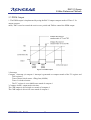
5.4 Output Waveforms for 120-Degree Commutation
1.Described below is an example of waveform output for 120-degree commutation that is
implemented through the use of the Timer C function.
120-Degree hall sensor
60-Degree hall sensor
TM1
Hall Sensor A
1
1
1
0
0
0
1
1
0
0
0
1
1
0
0
0
1
1
A
Hall Sensor B
B
Hall Sensor C
C
Up (CMP00 output)
Vp (CMP01 output)
Wp (CMP02 output)
Un (CMP10 output)
Vn (CMP11 output)
Wp (CMP12 output)
Figure 5.4 Sensor Inputs and Output Waveforms for 120-Degree Trapezoidal Wave Commutation
2.Three-phase output is implemented by port outputs and timer C compare match outputs.
TM1 interrupt
Up output(CMP00/P10 output)
Vp output(CMP01/P11 output)
For Up phase, a high level is output
by port output.
· Set port P1_0 to high level.
· Disable CMP00 output.
The Up phase output is changed from
port output to compare-match output.
· Set port P1_0 to high level.
· Enable CMP00 output.
For Vp phase, a low level is output by
compare-match output.
· Set port P1_1 to low level.
· Enable CMP01 output.
The Vp phase output holds the current
state.
· Set port P1_1 to low level.
· Enable CMP01 output.
RSSZEUM0001 – 0100
Rev.1.00
12
The Up phase output is changed to a
low level by compare-match output.
· Set port P1_0 to low level.
· Enable CMP00 output.
The Vp phase output is changed to a
high
level by port output.
· Set port P1_1 to high level.
· Disable CMP01 output.
R8C/11 Group
E-Bike Reference Platform
5.5 Speed control
In 120-degree commutation using trapezoidal waves, the speed of rotation is basically proportional
to the voltage.
The active period of the output waveform is controlled by rewriting the TM0
Detect handle A/D value and setting each time the rotation speed command is changed.
TM1
Slow
Fast
Output waveform
(duty cycle is set by TM0)
A/D input value
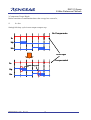
5.6 Commutation Current Control
1.120-Degree Trapezoidal Wave Commutation produces high torque ripple and audible noise ,
especially during transition of commutation. Because torque is directly proportional to current,
we wish to regulate torque (current) or shorten dynamic response time, motor current may be
regulated.
One of the simplest method of measuring current is inserting a low value resistor (Rs)
in the DC link path, negative of one of the phase current is detected.
Ia
Rs
RSSZEUM0001 – 0100
Rev.1.00
BLDC
Controller
13
R8C/11 Group
E-Bike Reference Platform
2.Compensate Torque Ripple
Before transition of commutation detect the average bus current Ia ,
if
Ia >Iset
Setting100% duty cycle in next output compare step.
No Compensate
Ia
Up
Un
current ripple
Compensated
Ia
100% duty cycle
Up
Un
RSSZEUM0001 – 0100
Rev.1.00
14
R8C/11 Group
E-Bike Reference Platform
5.7 MOSFET and Battery Protection
Detect Battery voltage
Vb ,Ia.
If Vb < Vset
Or Ia >Ia_set
Close the PWM output
Battery voltage Vb
Ia
BLDC
6. Bill of Components
Comment
Designator
Footprint
Quantity
Value
Cap Pol1
C1
CAPPR2-5x6.8
1
100pF
Cap
C2
C1608-0603
1
103
Cap
C3
C1608-0603
1
222
Cap Pol1
C4
CAPPR2-5x6.8
1
100uF/63v
RSSZEUM0001 – 0100
Rev.1.00
15
R8C/11 Group
E-Bike Reference Platform
Cap
C5
C1608-0603
1
103
Cap Pol1
C6
CAPPR2-5x6.8
1
100pF
Cap
C7
C1608-0603
1
222
Cap
C8
C1608-0603
1
103
Cap
C9
C1608-0603
1
103
Cap
C10
C1608-0603
1
222
Cap Pol1
C11
CAPPR2-5x6.8
1
100pF
Cap
C12
C1608-0603
1
103
Cap
C13
C1608-0603
1
103
Cap
C14
C1608-0603
1
103
Cap
C15
C1608-0603
1
103
Cap
C16
C1608-0603
1
103
Cap
C17
C1608-0603
1
103
Cap
C19
C1608-0603
1
103
Cap
C20
C1608-0603
1
103
Cap
C22
C1608-0603
1
103
Cap
C24
C1608-0603
1
103
Cap
C25
C1608-0603
1
104
Cap
C26
C1608-0603
1
104
Cap
C27
C1608-0603
1
104
Cap Pol1
C28
RB7.6-15
1
470uF/63V
Cap Pol1
C29
CAPPR2-5x6.8
1
47uF/63V
Cap Pol1
C30
CAPPR2-5x6.8
1
470uF/16V
Cap
C31
C1608-0603
1
103
Cap
C32
C1608-0603
1
104
Cap
C33
C1608-0603
1
103
Cap Pol1
C34
CAPPR2-5x6.8
1
470uF/25V
Cap
C35
CR0805
1
104
Cap
C36
CR0805
1
104
Cap
C37
CR0805
1
104
Cap
C38
C1608-0603
1
104
Cap
C39
C1608-0603
1
104
Cap
C40
C1608-0603
1
104
Cap
C41
C1608-0603
1
103
Cap
C42
C1608-0603
1
103
Cap
C46
C1608-0603
1
103
Header 7X2
CON1
HDR2X7
1
1N4007
D1
DSO-C2/X2.3
1
4148
D2
SO4148
1
1N4007
D3
DSO-C2/X2.3
1
4148
D4
SO4148
1
RSSZEUM0001 – 0100
Rev.1.00
16
R8C/11 Group
E-Bike Reference Platform
1N4007
D5
DSO-C2/X2.3
1
4148
D6
SO4148
1
4148
D7
SO4148
1
4007
D8
DSO-C2/X2.3
1
D Zener
D9
SO4148
1
D Zener
D10
SO4148
1
4148
D11
SO4148
1
4148
D12
SO4148
1
LED0
DS1
SMD _LED
1
5401
Q1
NPN
1
5551
Q2
NPN
1
5401
Q4
NPN
1
5401
Q6
NPN
1
5551
Q7
NPN
1
5401
Q9
NPN
1
5551
Q11
NPN
1
5401
Q12
NPN
1
5401
Q14
NPN
1
5401
Q16
NPN
1
5551
Q17
NPN
1
5551
Q18
NPN
1
5551
Q19
NPN
1
5401
Q20
NPN
1
5551
Q21
NPN
1
5551
Q22
NPN
1
5401
Q23
NPN
1
5551
Q24
NPN
1
5551
Q25
NPN
1
Res2
R1
C1608-0603
1
511
Res2
R2
C1608-0603
1
103
Res2
R3
C1608-0603
1
223
Res2
R4
C1608-0603
1
222
Res2
R5
C1608-0603
1
151
Res2
R6
C1608-0603
1
222
Res2
R7
C1608-0603
1
272
Res2
R8
C1608-0603
1
472
Res2
R9
C1608-0603
1
332
Res2
R10
C1608-0603
1
102
Res2
R11
C1608-0603
1
222
Res2
R12
C1608-0603
1
104
Res2
R13
CR1206
1
103
RSSZEUM0001 – 0100
Rev.1.00
17
R8C/11 Group
E-Bike Reference Platform
Res2
R14
C1608-0603
1
103
Res2
R15
C1608-0603
1
511
Res2
R16
C1608-0603
1
103
Res2
R17
C1608-0603
1
272
Res2
R18
C1608-0603
1
223
Res2
R19
C1608-0603
1
222
Res2
R20
C1608-0603
1
151
Res2
R21
C1608-0603
1
222
Res2
R22
C1608-0603
1
562
Res2
R23
C1608-0603
1
222
Res2
R24
C1608-0603
1
103
Res2
R25
C1608-0603
1
202
Res2
R26
C1608-0603
1
272
Res2
R27
C1608-0603
1
103
Res2
R28
CR1206
1
103
Res2
R29
C1608-0603
1
511
Res2
R30
C1608-0603
1
222
Res2
R31
C1608-0603
1
102
Res2
R32
C1608-0603
1
103
Res2
R33
C1608-0603
1
151
Res2
R34
C1608-0603
1
512
Res2
R35
C1608-0603
1
222
Res2
R36
C1608-0603
1
222
Res2
R37
C1608-0603
1
123
Res2
R38
C1608-0603
1
473
Res2
R39
C1608-0603
1
433
Res2
R40
C1608-0603
1
332
Res2
R41
C1608-0603
1
103
Res2
R42
C1608-0603
1
332
Res2
R43
CR1206
1
103
Res2
R44
C1608-0603
1
102
Res2
R45
C1608-0603
1
332
Res2
R46
C1608-0603
1
512
Res2
R47
C1608-0603
1
103
Res2
R48
C1608-0603
1
102
Res2
R50
C1608-0603
1
511
Res3
R51
AXIAL-0.5
1
Res2
R53
C1608-0603
1
215
Res2
R54
C1608-0603
1
472
Res2
R55
C1608-0603
1
151
Res2
R56
C1608-0603
1
222
RSSZEUM0001 – 0100
Rev.1.00
18
R8C/11 Group
E-Bike Reference Platform
Res2
R57
C1608-0603
1
332
Res2
R58
C1608-0603
1
223
Res2
R59
C1608-0603
1
472
Res2
R62
C1608-0603
1
102
Res2
R63
C1608-0603
1
332
Res2
R64
C1608-0603
1
332
Res2
R66
C1608-0603
1
153
Res2
R67
C1608-0603
1
472
Res2
R69
C1608-0603
1
511
Res2
R70
C1608-0603
1
153
Res2
R71
C1608-0603
1
151
Res2
R72
C1608-0603
1
222
Res2
R73
C1608-0603
1
102
Res2
R74
C1608-0603
1
511
Res2
R75
CR1206
1
751
Res2
R76
C1608-0603
1
151
Res2
R77
C1608-0603
1
222
Res2
R78
AXIAL-0.6
1
330/2W
Res2
R79
C1608-0603
1
102
Res2
R80
C1608-0603
1
103
Res2
R81
C1608-0603
1
102
Res2
R82
C1608-0603
1
103
Res2
R83
C1608-0603
1
103
Res2
R84
C1608-0603
1
103
Res2
R85
C1608-0603
1
223
Res2
R86
C1608-0603
1
102
Res2
R87
C1608-0603
1
512
Res2
R88
C1608-0603
1
472
Res2
R89
C1608-0603
1
473
Res2
R90
C1608-0603
1
104
Res2
R91
C1608-0603
1
103
Res2
R92
C1608-0603
1
103
Res2
R93
C1608-0603
1
103
M74HC11M1R
U1
SO14
1
LM324AD
U2
SO14
1
R8C/11
U3
TQFP32
1
LM317
VR1
SFM-T3/X1.6V
1
78L05
VR2
BCY-W3
1
RSSZEUM0001 – 0100
Rev.1.00
19
R8C/11 Group
E-Bike Reference Platform
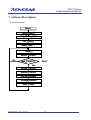
7. Software Description
7.1 main function
Main
Initialization
Init_Motor_sfr()
Init_Uart()
asm(“fset I”)
Timer()
Motor Control
No
sys_f1ms=1
;1ms?
Yes
Brake Control
Speed Control
Current Detect
Voltage Detect
Uart_sral()
RSSZEUM0001 – 0100
Rev.1.00
20
R8C/11 Group
E-Bike Reference Platform
7.2InitMcu
Init_MCU
CUP CLOCK Setting
asm("FCLR I");
//Interrupt disable
prc0=1;
//Protect off
cm05=1;cm02=0;cm14=0;ocd0=0;ocd1=0;
//On-chip oscillator selected(cm0 bit 2 and 5, cm1 bit 4, ocd bit 0 and 1)
ocd2=1;
//On-chip oscillator selected(ocd bit 2)
cm16=0;cm17=0;cm06=0;
//No division selected(cm0 bit 5,cm1 bit 6 and 7)
hr00=1;
hr01=1;
prc0=0;
//Protect on
I/O Setting
prc2=1;
pd0 |= 0x10;
pd0 &=0xbf;
pd4&=0x7f;
//enable write to pd0
// Port P0 direction register
//p00-02 as sensor input/
//p47 as break input
Timer X Setting 1ms no division
txck0=0;txck1=0;
prex=249;
tx=31;
txmod0=0;txmod1=0;
txic=5;
txs=1;
//count source:f1(tcss bit 0 and 1)
//Timer value for timer mode or half period timing for pulse
output mode
//Timer value for timer mode or half period timing for pulse
output mode
//Timer mode(txmr bit 0 and 1)
//start tx
1
RSSZEUM0001 – 0100
Rev.1.00
21
R8C/11 Group
E-Bike Reference Platform
1
adcon0 = 0x00;
adcon1 = 0x28;
adcon2 = 0x01;
// AN0 one-shot mode
// 10bit Vref connection
// sample & hold
Interrupt Setting
int0ic = 0x07;
inten = 0x01;
int0f = 0x00;
r0edg = 1;
int3ic=0x07;
tcc07=0;
tcc03=1;tcc04=0;
//int0 falling edge setting Level7
// int0 input enable one edge
// int0 no filter
// int1 falling edge setting
//Interrupt piority level 7 selected(int3ic bit 0-3)
//INT3 selected(tcc0 bit 7)
//falling edge setting
RTS
RSSZEUM0001 – 0100
Rev.1.00
22
R8C/11 Group
E-Bike Reference Platform
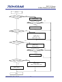
7.3 Initialize SFRs for Motor control
Init motor sfr
tcc0 = 0x16;
tcc1 = 0xec;
tcout = 0xbf;
p1 &= 0xf8;
pd1 |= 0x07;
p3 |= 0x07;
pd3 |= 0x07;
// TC count stop TC source:fRing-fast,
//no filter, TC register reset, output compare mode
//CMP00-CMP02 enable, CMP10-CMP12 enable
//CMP00-CMP02 OFF
//P10-P12: output, Low
// P30-P32 High
// P30-P32: output,
Motor_mode=Stop_mode;
Error_counter=0;
speed_act=90;
pwm_duty=START_DUTY;
Detect Sensor stage
RTS
7.4 Motor Control
RSSZEUM0001 – 0100
Rev.1.00
23
R8C/11 Group
E-Bike Reference Platform
_Motor()
Motor state= Stop
Yes
PWM Stop()
No
No
Speed command>Speed_start
Yes
Motor State = Start
Motor state= Start
Yes
Detect Sensor stage
_PWM_Set();
_PWM_OUT();
Motor State = Run
No
Yes
Motor state= Run
_PWM_Set();
PWM OUT();
No
Speed command<=Speed_start
Yes
Motor State = Stop
Motor state=Err
No
Yes
_PWM_Stop();
Motor_mode=Stop_mode
_PWM_Stop();
RTS
RSSZEUM0001 – 0100
Rev.1.00
24
No
R8C/11 Group
E-Bike Reference Platform
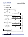
7.5 PWM Out processing
PWM_OUT
Yes
;Hall sensor is 120 DEG
Sensor option= 120 DEG
NO
; 60 DEG
SENSER_DEG0
2
Yes
; 0 DEG
No
SENSER_DEG60
Sensor stage = New Sensor stage
Out phase = PHASE_DEG0
Yes
; 60 DEG
No
SENSER_DEG120
Sensor stage = New Sensor stage
Out phase = PHASE_DEG60
Yes
; 120 DEG
No
SENSER_DEG180
Sensor stage = New Sensor stage
Out phase = PHASE_DEG120
Yes
; 180 DEG
No
SENSER_DEG240
No
;300 DEG
Sensor stage = New Sensor stage
Out phase = PHASE_DEG180
Yes
; 240 DEG
Sensor stage = New Sensor stage
Out phase = PHASE_DEG240
Sensor stage = New Sensor stage
Out phase = PHASE_DEG300
RTS
RSSZEUM0001 – 0100
Rev.1.00
25
R8C/11 Group
E-Bike Reference Platform
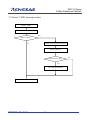
2
SENSER120_DEG0
Yes
; 0 DEG
No
SENSER120_DEG60
Sensor stage = New Sensor stage
Out phase = PHASE_DEG0
Yes
; 60 DEG
No
SENSER120_DEG120
Sensor stage = New Sensor stage
Out phase = PHASE_DEG60
Yes
; 120 DEG
No
SENSER120_DEG180
Sensor stage = New Sensor stage
Out phase = PHASE_DEG120
Yes
; 180 DEG
No
SENSER120_DEG240
No
Sensor stage = New Sensor stage
Out phase = PHASE_DEG180
Yes
; 240 DEG
;300 DEG
Sensor stage = New Sensor stage
Out phase = PHASE_DEG300
RTS
RSSZEUM0001 – 0100
Rev.1.00
26
R8C/11 Group
E-Bike Reference Platform
7.6 TimerC CMP1 interrupt routine
TimerC_CMP1
Sensor = Sersor_input()
Yes
Sensor Change
No
Sensor_state=New Sensor Statre
Current_Detect()
Current>Current_Set1
Yes
Set 100% Duty PWM
Reit
RSSZEUM0001 – 0100
Rev.1.00
27
No
R8C/11 Group
E-Bike Reference Platform
7.7 Short detection input (IN0)interrupt routine
Int0_()
NO
; INT0 P45 falling edge
P4_5 = 0
Yes
_PWM_Stop();
Motor_mode=ERR_mode
Reit
RSSZEUM0001 – 0100
Rev.1.00
28
R8C/11 Group
E-Bike Reference Platform
7.8 Over current detection input
(IN3)interrupt routine
Int3_()
NO
; INT0 P3_3 falling edge
P3_3 = 0
Yes
_PWM_Stop();
Motor_mode=ERR_mode
Reit
RSSZEUM0001 – 0100
Rev.1.00
29
R8C/11 Group
E-Bike Reference Platform
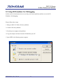
8. Using E8 Emulator for Debugging
In this section it demonstrates how to use the power meter platform, and how to use the E8
Emulator for debugging.
Please follow these steps:
1. Bring out R8C/11E-bike reference platform.
2. Connect E8 to the platform.
3. Provide power supply to the platform.
4. Copy the sample software from the CD-ROM to your PC.
5. Open HEW, the following picture appears.
RSSZEUM0001 – 0100
Rev.1.00
30
R8C/11 Group
E-Bike Reference Platform
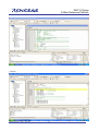
6. Choose the sample project.
RSSZEUM0001 – 0100
Rev.1.00
31
R8C/11 Group
E-Bike Reference Platform
7. Choose E8 Emulator, set emulator mode.
8. Build all.
RSSZEUM0001 – 0100
Rev.1.00
32
R8C/11 Group
E-Bike Reference Platform
9. Reset.
RSSZEUM0001 – 0100
Rev.1.00
33
R8C/11 Group
E-Bike Reference Platform
10. Run.
Now you can debug and evaluate the platform.
Note: About how to use HEW, please refer to the user manual of HEW.
.
RSSZEUM0001 – 0100
Rev.1.00
34
R8C/11 Group
E-Bike Reference Platform
R8C/11 E-bike reference Platform
User’s manual
Publication Date: Rev.1.00, Oct. 8, 2007
Published by: RS-SZ
Renesas Technology Corp.
Renesas System Solution
Edited by: RS-SZ
Renesas System Solution (Beijing) Co., Ltd Shenzhen Branch
©2007. Renesas Technology Corp., All rights reserved.
http://www.renesas.com
RSSZEUM0001 – 0100
Rev.1.00
35
R8C/11 Group
E-Bike Reference Platform
Notes regarding these materials
1.
2.
3.
4.
5.
6.
7.
8.
9.
10.
11.
12.
13.
This document is provided for reference purposes only so that Renesas customers may select the appropriate
Renesas products for their use. Renesas neither makes warranties or representations with respect to the
accuracy or completeness of the information contained in this document nor grants any license to any intellectual
property rights or any other rights of Renesas or any third party with respect to the information in this document.
Renesas shall have no liability for damages or infringement of any intellectual property or other rights arising out
of the use of any information in this document, including, but not limited to, product data, diagrams, charts,
programs, algorithms, and application circuit examples.
You should not use the products or the technology described in this document for the purpose of military
applications such as the development of weapons of mass destruction or for the purpose of any other military
use. When exporting the products or technology described herein, you should follow the applicable export
control laws and regulations, and procedures required by such laws and regulations.
All information included in this document such as product data, diagrams, charts, programs, algorithms, and
application circuit examples, is current as of the date this document is issued. Such information, however, is
subject to change without any prior notice. Before purchasing or using any Renesas products listed in this
document, please confirm the latest product information with a Renesas sales office. Also, please pay regular
and careful attention to additional and different information to be disclosed by Renesas such as that disclosed
through our website. (http://www.renesas.com)
Renesas has used reasonable care in compiling the information included in this document, but Renesas
assumes no liability whatsoever for any damages incurred as a result of errors or omissions in the information
included in this document.
When using or otherwise relying on the information in this document, you should evaluate the information in light
of the total system before deciding about the applicability of such information to the intended application.
Renesas makes no representations, warranties or guaranties regarding the suitability of its products for any
particular application and specifically disclaims any liability arising out of the application and use of the
information in this document or Renesas products.
With the exception of products specified by Renesas as suitable for automobile applications, Renesas products
are not designed, manufactured or tested for applications or otherwise in systems the failure or malfunction of
which may cause a direct threat to human life or create a risk of human injury or which require especially high
quality and reliability such as safety systems, or equipment or systems for transportation and traffic, healthcare,
combustion control, aerospace and aeronautics, nuclear power, or undersea communication transmission. If you
are considering the use of our products for such purposes, please contact a Renesas sales office beforehand.
Renesas shall have no liability for damages arising out of the uses set forth above.
Notwithstanding the preceding paragraph, you should not use Renesas products for the purposes listed below:
(1) artificial life support devices or systems
(2) surgical implantations
(3) healthcare intervention (e.g., excision, administration of medication, etc.)
(4) any other purposes that pose a direct threat to human life
Renesas shall have no liability for damages arising out of the uses set forth in the above and purchasers who
elect to use Renesas products in any of the foregoing applications shall indemnify and hold harmless Renesas
Technology Corp., its affiliated companies and their officers, directors, and employees against any and all
damages arising out of such applications.
You should use the products described herein within the range specified by Renesas, especially with respect to
the maximum rating, operating supply voltage range, movement power voltage range, heat radiation
characteristics, installation and other product characteristics. Renesas shall have no liability for malfunctions or
damages arising out of the use of Renesas products beyond such specified ranges.
Although Renesas endeavors to improve the quality and reliability of its products, IC products have specific
characteristics such as the occurrence of failure at a certain rate and malfunctions under certain use conditions.
Please be sure to implement safety measures to guard against the possibility of physical injury, and injury or
damage caused by fire in the event of the failure of a Renesas product, such as safety design for hardware and
software including but not limited to redundancy, fire control and malfunction prevention, appropriate treatment
for aging degradation or any other applicable measures. Among others, since the evaluation of microcomputer
software alone is very difficult, please evaluate the safety of the final products or system manufactured by you.
In case Renesas products listed in this document are detached from the products to which the Renesas products
are attached or affixed, the risk of accident such as swallowing by infants and small children is very high. You
should implement safety measures so that Renesas products may not be easily detached from your products.
Renesas shall have no liability for damages arising out of such detachment.
This document may not be reproduced or duplicated, in any form, in whole or in part, without prior written
approval from Renesas.
Please contact a Renesas sales office if you have any questions regarding the information contained in this
document, Renesas semiconductor products, or if you have any other inquiries.
© 2008. Renesas Technology Corp., All rights reserved.
RSSZEUM0001 – 0100
Rev.1.00
36