1
iSBC™ 208 FILEXIBLE DISK DRI"E
CO'NTROLLER
Hj~RDWARE
REFERIENCE MANUAL
Order Number: 143078-001
J
Copyright © 1981 Intel Corporation
Intel Corporation, 3065 B,)wers Avenue, Santa Clara, California 95051
r
Additional copies of this manual or other Intel literature may be obtained from:
Literature Department
Intel Corporation
3065 Bowers Avenue
Santa Clara, CA 95051
The information in this document is subject to change without notice.
Intel Corporation makes no warranty of any kind with regard to this material, including, but not limited
to, the implied warranties of merchantability and fitness for a particular purpose. Intel Corporation
assumes no responsibility for any errors that may appear in this document. Intel Corporation makes no
commitment to update nor to keep current the information contained in this document.
Intel Corporation assumes no responsibility for the use of any circuitry other than circuitry embodied in
an Intel product. No other circuit patent licenses are implied.
Intel software products are copyrighted by and shall remain the property of Intel Corporation. Use,
duplication or disclosure is subject to restrictions stated in Intel's software license, or as defined in ASPR
7-104.9(a)(9).
No part of this document may be copied or reproduced in any form or by any mmns without the prior
written consent of Intel Corporation.
The following are trademarks of Intel Corporation and its affiliates and may be used only to identify Intel
products:
BXP
CREDIT
i
ICE
iCS
.
'
1m
lnsite
ii
Inlel
in tel
lntelevision
Intellec
iRMX
iSBC
iSBX
Library Manager
MCS
Megachassis
Micromainframe
Micromap
Multibus
Multimodule
Plug· A-Bubble
PROMPT
RMX/SO
SYSlem2000
UPI
[A475/1081/
6[fu[1
REV.
-001
REVISION HISTORY
Original issue.
DATE
10/81
iii
PREFACE
I
This manual is the hardware referl~nce for the iSBC 208 Flexible Disk Controller.
The manual is divided into five chapters that describe general information,
preparation for use, programmingnformation, principles of operation, and service
information. Three appendices, describing sample 110 drivers, the iSBX
Multimodule interface, and drive interfaces are also included. Supplemental
information can be found in the following Intel publications:
•
•
•
•
•
•
Intel Multibus Specification, order number 9800683
iSBX Bus Specification, order number 142686
iSBC Applications Manual, oreler number 142687
Intel Component Data Catalog
MCS-80/85 Family User's Manual, order number 121506
The 8086 Family User's Manual, order number 9800722
8080/8085 Assembly Language Programming Manual,
•
MCS-86 Macro Assembly Language Reference Manual
•
order number 9800940
order number 9800640
v
CONTENTS
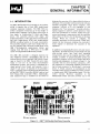
CHAPTER 1
GENERAL INFORMATION
PAGE
Introduction ...................... " .......... .
Specifications
1-1
1-2
CHAPTER 2
PREPARATION FOR USE
Introduction ................................. .
Unpacking and Inspection .................. .
Installation Considerations .................... .
Powt:r Requirements ........................ .
Cooling Requirements ...................... .
Bus Interface .................................
Multibus Interface AC Characteristics ......... .
Multibus Interface DC Characteristics ......... .
Auxiliary Connl~ctor ........................ .
Board Location Considerations ................. .
Controller Board Configuration ................ .
Host Processor Configuration ................ .
Drive Configuration ........................ .
Auxiliary Port Configuration .......... " ..... .
Drive Interfacing ............................. .
Controller Interface Signals .................. .
Drive Interface AC Characteristics ............ .
Drive Interface DC Characteristics ............ .
Drive Cabling ................................ .
Drive Modifications .......................... .
Ready Logic ............................... .
Motor-On Control ......................... .
Radial Head Load .......................... .
Drive Termination .......................... .
Drive Numbering ........................... .
Multiple Drive Pin Assignments .............. .
Stepper Motor Power ....................... .
2-1
2-1
2-1
2-1
2-1
2-1
2-1
2-1
2-7
2-7
2-8
2-8
2-9
2-11
2-11
2-11
2-11
2-11
2-17
2-18
2-18
2-18
2-18
2-18
2-18
2-18
2-18
CHAPTER 3
PROGRAMMING INFORMATION
Introduction ................................. .
UO Port Commands ...........................
Read/Write DMAC Address Registers... .... ...
Read/Write DMAC Word Count Registers ......
Write DMAC Command Register ..............
Read DMAC Status Register Command ........
Write DMAC Request Register .................
Set/Reset DMAC Mask Register ...............
Write DMAC Mode Register ..................
Clear DMAC First/Last Flip-Flop .............
DMAC Master Clear .........................
Write DMAC Mask Register ..................
Read FDC Status Register .....................
Read/Write FDC Data Register ................
Write Controller Auxiliary Port ...... ,........
Poll Interrupt Status ................ '........
3-1
3-1
3-1
3-3
3-3
3-3
3-4
3-4
3-4
3-5
3-5
3-5
3-6
3-6
3-6
3-7
I
PAGE
Controller Reset ........................... . 3-7
Write Controller Low- And High-Byte Segment
Address Registers ...................... . 3-8
Diskette Organization ......................... . 3-8
FDC Commands ............................ ". 3-12
Specify Command .......................... . 3-16
Seek Command ............................. 3-17
Read Data ................................ . 3-17
Read Deleted Data .......................... 3-19
Read ID ................................... 3-20
Read Track ................................ . 3-20
Write Data ................................ . 3-21
Write Deleted Data ..... . .................... 3-21
Format Track .............................. . 3-21
Recalibrate
3-23
Sense Drive Status .......................... . 3-24
Sense Interrupt Status ....................... . 3-24
Invalid Commands ......................... . 3-24
Software ..................................... 3-24
Initialization .............................. . 3-25
Programming the DMAC .................... . 3-25
Programming the FDC ...................... . 3-25
Interrupt Processing ....................... . 3-28
CHAPTER 4
PRINCIPLES OF OPERATION
Introduction
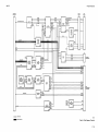
Schematic Interpretation ...................... .
Functional Description ........................ .
Clock and Timing Circuitry .................. .
Multibus Interface .......................... .
DMA Controller (DMAC) ................... .
DMA Addressing .......................... .
Floppy Disk Controller ...................... .
FDD Interface ............................. .
Drive and Head Selection .................. .
Write Precompensation ................... .
Data Separator ... , ...................... .
4-1
4-1
4-1
4-1
4-2
4-3
4-3
4-4
4-5
4-5
4-5
4-5
CHAPTER 5
SERVICE INFORMATION
Introduction
Service and Repair Assistance ...................
Replaceable Parts .............................
Adjustments ..................................
Service Diagrams ..............................
5-1
5-1
5-1
5-1
5-1
APPENDIX A
SAMPLE DRIVERS
Introduction .................................. A-I
PUM 86 Driver ............................... A-I
Assembly Language Driver ..................... A-15
vii
CONTENTS (Cont'd.)
APPENDIXB
iSBX MUL TIMODULE BOARD
INTERFACE
PAGE
PAGE
Port Assignments ...........................
Programming the DMAC ....................
Introduction. . . . . . . . . . . . . . . . . . . . . . . . . . . . . . . . ..
Installation ...................................
Configuration ................................
DMA Channels .............................
Interrupts ..................................
Programming Information .....................
B-1
B-1
B-1
B-1
B-2
B-2
B-2
B-2
APPENDIXC
DRIVE INTERFACES
Introduction ..................................
U sing the Tables ..............................
C-I
C-I
TABLES
TABLE
1-1
2-1
2-2
2-3
2-4
2-5
2-6
2-7
2-8
2-9
2-10
2-11
2-12
2-13
3-1
3-2
viii
TITLE
PAGE
Specifications .........................
Multibus Interface Pin Assignments ......
Multibus Interface Signal Definitions .....
iSBC 208 Board DC Characteristics ......
P2 Bus Connector .....................
110 Base Address Selection .............
Drive Configuration Jumper Links .......
Auxiliary Port Jumper Matrix ...........
12 Interface Connector Pin Assignments ..
Jl Interface Connector Pin Assignments ..
Interface Connector Signal Functions ....
Drive Interface AC Timing Characteristics
Drive Interface DC Characteristics .......
Mating Connectors ....................
I/O Port Controller Commands .........
Track Format .........................
1-2
2-2
2-3
2-6
2-7
2-9
2-9
2-11
2-13
2-13
2-14
2-16
2-16
2-17
3-2
3-10
TABLE
3-3
3-4
3-5
3-6
3-7
3-8
3-9
3-10
3-11
3-12
4-1
4-2
4-3
4-4
5-1
5-2
TITLE
PAGE
Recording Capacities ..................
FDC Commands ......................
Result Phase Status Registers ............
Command Mnemonics .................
HUT Values ..........................
SRT Values ..........................
HLT Values ..........................
Command Byte Values .................
Result Phase 10 Information ............
Formatting Table .....................
IC U71 Output ........................
Write Clock Frequency .................
Chip Select Coding ....................
On Time Clock Versus Data Rate ........
Replaceable Parts .....................
Manufacturer's Codes .................
3-12
3-12
3-13
3-15
3-16
3-17
3-17
3-18
3-19
3-23
4-2
4-2
4-2
4-6
5-2
5-4
ILLUSTRATIONS
FIGURE
1-1
2-1
2-2
2-3
2-4
2-5
2-6
2-7
2-8
3-1
3-2
3-3
3-4
TITLE
PAGE
iSBC 208 Flexible Disk Drive Controller
Bus Acquisition and Memory
Transfer Timing ....................
I/O Transfer Timing ...................
Serial Priority Resolution ...............
Typical Four-Drive System (Standard-Sized
Drives) .............................
Seek Timing ..........................
Head Load Timing ....................
Write Data Timing ....................
Flat-Ribbon I/O Interface Cable .........
Main Status Register Timing ............
20-Bit Addressing .....................
Track Format .........................
Sector Interleaving ....................
1-1
2-4
2-5
2-8
2-12
2-15
2-15
2-15
2-17
3-7
3-8
3-9
3-22
FIGURE
3-5
3-6
3-7
3-8
3-9
3-10
4-1
4-2
4-3
4-4
5-1
5-2
TITLE
PAGE
I/O Parameter Block ..................
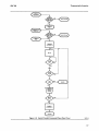
Initialization Flow Chart ...............
FOC Command Phase Flow Chart .......
Serial/Parallel Command Phase
Flow Chart .........................
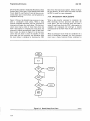
Result Phase Flow Chart ...............
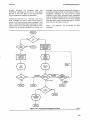
Interrupt Processing Flow Chart .........
Logic Conventions ....................
DMA Transfer Timing .................
Data Recovery Timing .................
Block Diagram of Controller ............
iSBC 208 Parts Location Diagram ........
iSBC 208 Board Schematic Drawing
(7 sheets) ...........................
3-25
3-26
3-26
3-27
3-28
3-29
4-1
4-4
4-6
4-7
5-5
5-7
IX
l
11
CHAPTER
GENERAL INFORMATION
,----~-
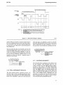
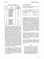
1-1. INTRODUCTION
The iSBC 208 Flexible Disk Controller is one product
within a complete line of Intel iSBC single board
computer expansion modules. The iSBC 208 controller is designed to interface up to four single- or
double-sided, standard 8-inch floppy disk drives or
four single- or double-sided 5 'i4 -inch mini-floppy
drives. The controller permits both single- and
double-sided drives of the same size to be interfaced,
and both single-delilsity (FM) and double-density
(MFM) recording formats to be used concurrently.
The controller supports a soft-sector format with sector sizes ranging from 128 bytes to 409~ bytes in the
IBM 3740-compatible single-density format and
ranging from 256 bytes to 8192 bytes in the IBM
system 34-compatible double-density format.
The iSBC 208 controller is designed expressly for
Intel Multibus interface compatibility and can be
inserted directly into a standard iSBC 604/614 cardcage as found in the iSBC System 80 series mainframe or into any of the Intel microcomputer
development systems. All circuitry is contained on a
single printed circuit board and operates from a
single +5 volt source. A majority of the controller's
logic is LSI (large scale integration) and includes both
an Intel 8237 DMA Controller (DMAC) and an Intel
8272 Floppy Disk Controller (FDC). Additionally,
data separation logic is included on the board to
MINI-DRIVE
INTERFACE
Pl
MlILTlBUS·MINTERFACE
eliminate the necessity of this logic within the drive or
off-board. The controller interfaces directly with any
multibus-compatible single board computer. This
computer, referred to in the remainder of this
manual as the "host processor," provides all information required to perform a disk operation. Once
all of the information is received, further host processor involvement is unnecessary, and the controller
takes control of the bus for the duration of the data
transfer. When the transfer is complete, the
controller interrupts the host processor. When interrupted, the host processor examines the controller's
status register to determine the outcome of the
operation.
In addition to programmable sector sizes and recording density, the head load time, head unload time and
track-to-track access time (step rate) operating
characteristics also can be program specified. Additionally, a number of jumper-selectable options are
provided to support various drive features and drive
interface pin assignments. As shown in figure 1-1, the
controller has two drive-interface connectors, -a 50pin connector for interfacing standard 8-inch drives
and a 34-pin connector for interfacing 5 'i4 -inch mini
drives. A 36-pin connector is incorporated on the
controller board for the installation of either a singleor double-wide iSBX Multimodule board. The controller extends M ultibus capability to the
Multimodule board and also provides up to two
STANDARD-DRIVE
INTERFACE
iSBX T• MULTIMODULP"
INTERFACE
J2
J3
P2
AUXILIARY INTERFACE
Figure 1-1. iSBcrM 208 Flexible Disk Drive Controller
143078-1
1-1
General Information
iSBC 208
DMA channels for use by the iSBX board. The P2
auxiliary edge connector includes four address lines
that extend the controller's memory addressing
capability to 16 megabytes (24-bit address bus).
1·2. SPECIFICATIONS
Table 1-1 lists the physical and performance
characteristics of the iSBC 208 controller.
Table 1-1. Specifications
Compatibility
Host Processor
Any Intel mainframe, microcomputer development system or Multibus-compatible
CPU. The controller supports either 16-,20- or 24-bit addresses and an 8-bit data
bus width.
Diskette Drive
Single- or double-sided, standard 8-inch or 5%-inch mini drives. Up to four drives
of one size can be interfaced; single- and double-density, and single- and doublesided drives can be mixed.
Drive Interface
Compatible with Shugart SA850 (standard 8-inch) and Shugart SA450 (5%-inch
mini) or any other drive with a similar interface.
Typical Drive Characteristics
Transfer Rate
Standard 8-inch Drive
250 kilobits per second, single density (FM)
500 kilobits per second, double density (MFM)
5%-inch Mini Drive
125 kilobits per second, single density (FM)
250 kilobits per second, double density (MFM)
Disk Speed
360 rpm (standard 8-inch)
300 rpm (5%-inch mini)
Track-to Track Access Time (Step Rate)
Programmable from 1 to 16 ms in 1 ms steps (standard) or from 2 to 32 ms in 2 ms steps (mini).
Head Load Time
Programmable from 2 to 254 ms in 2 ms increments (standard) or from 4 to 508 ms in 4 ms increments (mini).
Head Unload Time
Programmable from 16 to 240 ms in 16 ms increments (standard) or from 32 to 480 ms in 32 ms increments (mini);
jumper selectable for 1 second.
Physical
Dimensions
Length: 30.48 cm (12.0 inches)
Width: 17.15 cm (6.75 inches)
Height: 1.27 cm (0.5 inches)
Shipping Weight
0.82 kg (1.8 pounds)
Power Requirements
5.0 volts (±5%), 3 amperes (maximum)
Environmental
Temperature: O°C to +55°C, operating (+32°F to +131 OF)
-55°C to +85°C, non-operating (-67°F to +185°F)
Humidity:
1-2
Up to 90% relative humidity without condEmsation.
General Information
iSBC 208
Table 1-1. Specifications (Cont'd.)
Data Organization and Capacity (Standard 8-inch drives')
Single Density
IBM Format
N,on-IBM Format
Bytes per Sector
Sectors per Track
Tracks per Side
Bytes per Side
128
256
512
26
15
8
77
77
77
256,256 (128-byte sector)
295,680 (256-byte sector)
315,392 (512-byte sector)
1024
2048
4096
4
2
1
2Ei6 Addressable
315,392 (77 tracks)
Double Density
IBM Format
Non-IBM Format
Bytes per Sector
Sectors pHr Track
Tracks per Side
Bytes per Side
1024
512
256
15
8
26
77
77
77
512,512 (256-byte sector)
591,360 (512-byte sector)
630,784 (1 024-byte sector)
2048
4
2~i6
4096
8192
2
1
Addressable
630,784 (77 tracks)
'Consult manufacturer's data for mini-floppy drive organization and capacity.
1-3
CHAPTER 2
PREPARATION FOR USE
2-1. INTRODUCTION
This chapter presents information on the preparation
and installation of the iSBC 208 Controller. Included
within this chapter are instructions describing the
unpacking and inspection, installation, board configuration, host processor bus interface and drive
cabling for the controller.
2-2. UNPACKING AND INSPECTION
On receipt of the controller from the carrier,
immediately inspect the shipping carton for evidence
of mishandling in transit. If the shipping carton is
damaged or waterstained, request that the carrier's
agent be present when the carton is opened. If the
carrier's agent is not present when the carton is
opened and if the contents of the carton are
damaged, keep the carton and packing materials
intact for the agent's inspection.
For repairs or replacement of an Intel product
damaged in shipment, contact the Intel Technical
Support Center (see Chapter 5) to obtain a Return
Authorization Number and further instructions. A
copy of the purchase order should be submitted to
the carrier with the claim.
Carefully unpack the shipping carton and verify that
the following items are included. Compare the
packaging slip with your purchase order to verify
that the order is complete. The carton and packing
materials should be saved in case it becomes
necessary to reship the controller at a later date.
Item 1: iSBC 208 Interface Printed Circuit
Assembly.
Item 2: Schematic Diagram.
2-3. INSTALLATION
CONSIDERATIONS
The controller is designed expressly for installation
into the Intel iSBC 604/614 modular backplane and
card cage as found in the Series 80 single board computer mainframes. The controller can also be installed
into any odd-numbered slot in an Inteillec Model 800
or in any slot in an Intellec microcomputer development system. The controller additionally can be
installed into a user's Multibus-compatible
backplane assembly that meets the controller's
mating connector dimensional requirements.
2-4. POWER REQUIREMENTS
The controller operates from a single +5 volt (±5 070)
source and requires a maximum of 3.0 amperes.
When installing the interface in an iSBC 80 Series,
microcomputer development, or custom system,
ensure that the system"s power supply can meet the
additional current requirements of the controller.
2-5. COOLING REQUIREMENTS
The iSBC 80 Series and Intellec microcomputer
development systems use forced-air cooling that
generally is adequate to maintain an internal
operating temperature below 55°C. When installing
the controller in a high-temperature environment or
in any other system enclosure, ensure that the internal operating temperature is not permitted to exceed
the 55°C maximum.
2-6. BUS INTERFACE
The controller communicates with the host processor
(and memory) via the Mulilibus interface. Tables 2-1
and 2-2 define the Multibus interface pin assignments
and corresponding signal definitions. The controller
connects to the Multibus interface through connector
PI, an 86-pin, double-sided printed circuit edge connector with 3.96mm (0.156 inch) contact centers.
2-7. MUL TIBUS INTERFACE
AC CHARACTERISTICS
Figures 2-1 and 2-2 show the Multibus interface ac
timing characteristics when the controller is
operating as a "bus mastl~r" (Bus Acquisition and
Memory Transfer Timing) and as a "bus slave" (110
Transfer Timing).
2.8 MUL TIBUS INTERFACE
DC CHARACTERISTICS
The controller's dc signal characteristics for the
Multibus interface are given in table 2-3.
2-1
Preparation for Use
iSBC 208
Table 2-1. Multibus Interface Pin Assignments
Pin"
Signal
1
2
3
4
5
6
7
8
9
10
11
12
13
14
15
16
17
18
19
20
21
22
23
24
25
26
27
28
29
30
31
32
33
34
35
36
37
38
39
40
41
42
43
GND
GND
+5VDC
+5VDC
+5VDC
+5VDC
+12VDC
+12VDC
GND
GND
BCLK!
INIT!
BPRN!
BPRO!
BUSY!
BREQ!
MRDC!
MWTC!
10RC!
10WC!
XACK!
Function
}
}
}
Power Inputs
Ground
Bus Clock
Initialization
Bus Priority In
Bus Priority Out
Bus Busy
Bus Request
Memory Read Command
Memory Write Command
110 Read Command
I!O Write Command
Transfer Acknowledge
ADR10!
CBRQ!
ADR11!
CCLK!
ADR12!
Address Bus
Common Bus Request
Address Bus
Constant Clock
Address Bus
ADR13!
INT6!
INH!
INT4!
INT5!
INT2!
INT3!
INTO!
INT1!
ADRE!
Address Bus
Interrupt Request 6
Interrupt Request 7
Interrupt Request 4
Interrupt Request 5
Interrupt Request 2
Interrupt Request 3
Interrupt Request 0
Interrupt Request 1
Address Bus
'Unassigned Pins are reserved.
2-2
Ground
Pin"
44
45
46
47
48
49
50
51
52
53
54
55
56
57
58
59
60
61
62
63
64
65
66
67
68
69
70
71
72
73
74
75
76
77
78
79
80
81
82
83
84
85
86
Signal
Function
ADRF! ....
ADRC!
ADRD!
ADRAI
ADRB
ADR8!
ADR9!
ADR6!
~
ADR7!
ADR4!
ADR5!
ADR2!
ADR3!
ADRO!
ADR1! J
DAT6! ...
DAH!
DAT4!
DAT5!
DAT2!
DAT3!
DATO!
DAT1! J
GND
}
GND
-12VDC
-12VDC
+5VDC
+5VDC
+5VDC
+5VDC
GND
GND
>
Address Bus
Data Bus
Ground
}
Power Inputs
}
Ground
Preparation for Use
iSBC 208
Table 2-2. Multibus Interface Signal Definitions
Signal
Function
ADRO/-ADRFI
Address. These ·,6 bidirectional lines specify the address of the memory location or
110 port to be accessed. ADRF I is the most significant bit.
ADR10/-ADR131
Extended Address. These four output lines extend the controller's memory
addressing to 1 megabyte. ADR131 is the most significant bit.
BCLKI
Bus Clock. This input signal is used to synchronize the controller's bus control logic.
BPRNI
Bus Priority In. This input signal level indicates that no higher-priority master board
has requested control of the bus.
BPROI
Bus Priority Out. This output signal level is used with serial priority resolution
schemes and indicates to the next lower-priority master board that either the controller or another higher-priority master board has requested control of the bus.
BREQI
Bus Request. Thils output signal is used with parallel priority resolution schemes and
indicates that the controller is requesting control of the bus.
BUSYI
Bus Busy. This bidirectional signal indicates that either the controller or another
master board is currently in control of the bus and consequently prevents any other
master board from gaining access to the bus.
CBRQI
Common Bus Request. This output signal indicates that the controller requires
access to the bus while the bus is in the use by another bus master.
CCLKI
Constant Clock. A clock signal routed through the controller to the iSBX
multimodule.
DATO/-DAT71
Data. These eight bidirectional lines transfer data either to or from the memory
location or 110 port addressed. DA T71 is the most significant bit.
INITI
Initialization. This input signal generally originates from a power-up reset circuit or a
contact closure to ground (Le., a front panel reset switch) and resets all devices on
the bus to an initialized state.
INTO/-INT71
Interrupt. A set of eight, mUlti-level interrupt request lines for use with parallel
interrupt resolution logic. The selected (jumper determined) output interrupt signal
is used to indicate a controller-initiated interrupt request.
10RCI
110 Read Command. This input signal instructs the controller to place the data
associated with the addressed input port onto the data lines.
10WCI
110 Write Command. This input signal instructs the controller to accept the data
associated with the addressed output port that is present on the data lines.
MRDCI
Memory Read Command. This output signal indicates that the address of a memory
location is on the address lines and that the contents of that location are to be placed
on the data lines for acceptance by the controller.
MWTCI
Memory Write Command. This output signal indicates that the address of a memory
location is on the address lines and that the data presented by the controller on the
data lines is to be written into that location.
XACKI
Transfer Acknowledge. This signal originates from the controller during 110 port
transfers and indicates that the controller has accepted or is presentinrl the
associated data of' the data lines. During memory transfers, this Signal originates
from the random access memory board and indicates that the data on the data lines
either has been written into the addressed memory location or that the data is
present and is to be accepted by the controller.
2-3
Preparation for Use
iSBC208
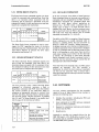
BCLKI
BREOI
~
BREO
\I_tBR_EO_ . . . : . . -_ _ _ _I - . : . . . J F t
~tBPRO
-...j
"BPROI - - "BUSYI
<I
---t
~tBUSY
j...-tBPRO
' ' ' ' ' - - - - - - . . ; . I - I - - - tB-US- Y-
\
-I
1
---~~----------------~
__________
-_I_ _ , . ' - tCBRO
!;::tCBRO
CBROI
\
ADROI - ADR131 _ _ _ _ _ _ _ _ _
1
_ _ _ _ _ _ _ _ _ _ _ _ _ _ _ _ _- J
~~..- - - - - - S T A B L E ADDRESS-----___..x'"""'_______
,__
tAS_R_ _ _ _ _
l'b--tAH
MRDCI OR 10RCI
DATOI-DATlI
I
1;::::= tDXL
---------------""'x:
~tASW9
MWTCI OR 10WCI
:::::I
DATOI - DATl I - - - - - - - - - - - - -
-I..
!-==tDSW
I
*'
-----1-------
tXCR:::::!
STABLE READ DATA
l---tXCW~
tDHR
I-'DHW
.x."-------
~lf....---STABLE WRITE DATA---....
'---~/
XACKI
• ASSUMES BPRNI ACTIVE
Parameter
tCBRO
tBCY
tBW
tBREO
tBPRNS
tBPRO
tBPRNO
tBUSY
tASR
tAH
tDXl
tXCR
tDHR
tASW
tDS
txcw
tDHW
tlNIT
Minimum
Maximum
67 ns
100 ns
35 ns
35 ns
22 ns
40 ns
30 ns
55ns
286 ns
147 ns
-250 ns
567ns
-80 ns
786 ns
80 ns
567ns
65ns
4 ns
1327 ns
1257 ns
Description
BClKI to CBROI Delay
Bus Clock Period
Bus Clock Pulse Width
BClK/ to BREO/ Delay
BPRN / to BClKI Setup Time
BClK/ to BPRO/ Delay
BPRN/ to BPRO/ Delay
BClK/ to BUSY/low Delay
Address Setup Time (Read)
Address Hold Time
Data Setup to Acknowledge Time (Read)
Acknowledge to Command High (Read)
Data Hold Time (Read)
Address Setup Time (Write)
Data Setup to Command Time (Write)
Acknowledge to Command High-(Write)
Data Hold Time (Write)
Reset Pulse Width
Figure 2-1. Bus Acquisition and Memory Transfer Timing
2-4
121746-2
Preparation for Use
iSBC 208
ADDRESS/
WRITE DATAl
~
ADDRESS STABLE
~'''-1
J-t
r-''"~
+-3
'"1
¥ DATASTAB~Er-'--3
DATA STABLE
~'''--1
READ DATA/
COMMAND/
(IORC/ OR IOWC/)
~------3
I
~
'XACK
XACK/
Parameter
Minimum
tAS
tAH
tXACK
,tXACK
tDXL
tDHR
tXAH
tDS
tOH
-384 ns
50 ns
906 ns
4400 ns
2 ns
20 ns
61 ns
-189 ns
35 ns
r'""-1 rr,""'1
X ~
\~
Maximum
1100 ns
5100 ns
~'''"!
Description
Address Setup Time
Address Hold Time
Command to Acknowledge
Read Data Setup Time
Read Data Hold Time
Acknowledge Hold Time
Write Data Setup Time
Write Data Hold Time
'Software RESET command only.
Figure 2-2. 110 Transfer Timing
143078-2
2-5
Preparation for Use
iSBC 208
Table 2-3. iSBC 208 Board DC Characteristics
Signals
XACKI
ADRO/ADRFI
Symbol
VOL
VOH
V IL
V IH
IlL
IIH
'C L
Output Low Voltage
Output High Voltage
Input Low Voltage
Input High Voltage
Input Current at Low V
Input Current at High V
Capacitive Load
VOL
V OH
V IL
V IH
IlL
Output Low Voltage
Output High Voltage
Input Low Voltage
Input High Voltage
Input Current at Low V
Input Current at High V
Capacitive Load
·6
H
L
BCLK/,
BPRNI
V IL
V IH
IlL
Input Low Voltage
Input High Voltage
Input Current at Low V
Input Current at High V
Capacitive Load
·6
H
L
ADR10/ADR131
VOL
V OH
V LL
ILH
Output Low Voltage
Output High Voltage
Output Leakage Low
Output Leakage High
Test
Conditions
IOL =32 rnA
IOH=-5.2 rnA
IOL =32 rnA
IOH=-5 rnA
V IN =-0.45 V
V IN =5.25V
0.8
V IN =0.45V
V ln =5.25V
IOL =24 rnA
IOH=-15 rnA
IOL =3.2 rnA
IOH=-0.4 rnA
VOL
V OH
'C L
Output Low Voltage
Output High Voltage
Capacitive Load
IOL =20 rnA
IOH=-0.4 rnA
Output Low Voltage
Input Low Voltage
Input High Voltage
Input Current at Low V
Input Current at High V
IOL=20 rnA
DATO/-
DAT71
CBRQI
(Open
Collector)
IORC/,
IOWC/,
INIT/,
CCLKI
H
L
V,x
'C IL
V IL
V IH
IlL
.~I
L
-0.5
100
15
0.4
-
Output Low Voltage
Output High Voltage
Input Low Voltage
Input High Voltage
Input Current at Low V
Output Leakage High
Capacitive Load
Output Low Voltage
Capacitive Load
Input Low Voltage
Input High Voltage
Input Current at Low V
Input Current at High V
Capacitive Load
V
V
V
V
rnA
IJA
pF
V
V
V
V
rnA
IJA
pF
V
V
rnA
IJA
pF
20
20
15
pF
0.45
V
V
pF
2.4
15
0.45
2.4
10
0.45
0.8
2.0
V IN =0.45V
V IN =5.25V
Units
V
V
IJA
IJA
2.4
-0.5
100
20
Capacitive Load
VOL
V OH
V 1L
V "H
IlL
·6
-0.2
50
18
2.0
Output Low Voltage
Output High Voltage
Capacitive Load
H
L
0.45
2.4
0.8
VOl.
VOH
'C L
·6
-1.2
40
15
2.0
BPROI
VOl.
V IL
V IH
V IL
.04
2.0
V IN =0.4V
VIN=2.4V
Capacitive Load
BUSYI
(Open
Collector)
Max
0.8
'C L
-
Min
2.0
ADR14/ADR17I
(on P2)
BREQI
2-6
Parameter
Description
V
V
V
rnA
IJA
pF
VIN =0.45V
Vo =5.25V
-'0.20
100
18
V
V
V
V
rnA
IJA
pF
10L =60 rnA
0.8
15
V
pF
0.8
V
V
rnA
flA
pF
IOL=32 rnA
IOH=-5 rnA
0.45
V
V
pF
2.4
0.80
2.0
2.0
V IN =O.4V
V IN =2.4V
-1.2
40
18
iSBC 208
Preparation for Use
Table 2-3. iSBC™ 208 Board DC Characteristics (Cont'd.)
Signals
INTO/INT71
VOL
VOH
ILH
.~L
L
MRDC/,
MWTCI
Parameter
Description
Symbol
VOL
VOH
V IL
VIH
10
·C L
Test
Conditions
Output Load Voltage
Output High Voltage
Output Leakage High
Output Leakage Low
Capacitive Load
IOL=60 mA
Open Collector
Vo =5.25V
Vo=0.45V
Output Low Voltage
Output High Voltage
Input Low Voltage
Input High Voltage
Output Leakage Current
IOL=32 mA
IOH=-2 mA
Capacitive Load
Min
Max
0.45
V
250
-500
15
flA
pF
0.45
2.4
0.8
2.0
VIN =0.45V
VIN =5.25
Units
-100
100
25
flA
V
V
V
V
flA
flA
pF
·Capacitive load values are approximations .
2-9. AUXILIARY CONNECTOR
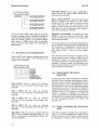
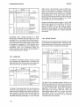
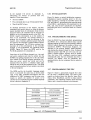
The auxiliary connector (P2) provides the four 1megabyte paging bits to effectively allow the controller to address up to 16 megabytes. The bits are set
in the controller's auxiliary port and are routed to the
P2 connector as noted in table 2-4.
illustration (figure 2-3), a wire-wrap jumper must be
installed from terminal post B (BPRN/) to logic
ground at terminal post N (604) or terminal post L
(614).
Always remove system power prior to
installing or removing a board in the
backplane. Failure to observe this precaution can result in circuit damage.
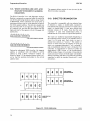
2-10. BOARD LOCATION
CONSIDERATIONS
Since the controller functions as a bus master during
DMA transfers, when installing the controller in a
serial priority environment (e.g., within any of the
Intel Series 80 mainframes), the controller should
occupy the highest priority slot (top physical slot) in
the 604/614 backplane and card cage assembly, with
any other bus masters and the host processor board
located below. The backplane providl~s bus priority
in and out s~nal continuity among adjacent bus
masters. The BPRNI (Bus Priority In) input to the
top slot (12) of either the single (604) or expansion
(614) backplane must be connt~cted to logic ground.
Both backplanes provide the BPRNI input on a wirewrap terminal post. As shown in the following
Note that if a bus slave (e.g., a memory board) is
installed between two bus masters (or if a vacant slot
exists between two bus masters), the serial priority
input-output chain must be physically jumpered on
the backplane to maintain signal continuity. Figure
2-3 shows the installation of a jumper between
terminal posts C and E that would provide the
required BPROI-BPRNI continuity around a
"slave" installed in the second slot (13).
When installing the controller in a parallel priority
resolution environment, the controller should be
given the highest bus priority . In an Intellec Model
Table 2-4. P2 Bus Connector
DC Characteristics (each signal)
Pin
56
55
58
57
Signal
ADR171
ADR161
ADR151
ADR141
Function
Current Drive
Current Load
Low (I OL )
High (loHI
Low (IlL)
High (IIHI
24mA
-15mA
0
0
High-Order Page Address Bit
Low-Order Page Address Bit
2-7
Preparation for Use
iSBC208
HIGHEST PRIORITY
J2
J3
LOWEST PRIORITY
J5
J4
10 1 10 1 10 1 10 1
15
15
15 N.C.
BPRNI
BPROI
16
N.C.
16
15 N.C.
BPRNI
BPROI
16
~"~J
N.C.
Jl-16 (614)
10 J 10 J 10 J 10 J
iSBC 208
CONTROLLER
iSBC 1/0
BOARD
(TYPICAL)
iSBC CPU
BOARD
(TYPICAL)
C
E
INSTALL
JUMPER
INSTALL
JUMPER
--
--
l
L(M)
--
TERMINAL POST DESIGNATIONS IN PARENTHESES
CORRESPOND TO 614 EXPANSION BACKPLANE
iSBC RAM
BOARD
(TYPICAL)
H
K(N~
--
Figure 2-3. Serial Priority Resolution
800 development system, the controller must be
installed in an odd-numbered (bus master) slot and
ideally should be installed in slot 17 (highest bus
priority). In an Intellec Series II or Series III development system, the controller should be installed in the
bottom (highest bus priority) slot.
2-11. CONTROLLER BOARD
CONFIGURATION
The controller board includes alterable jumpers that
are used to configure the controller to its intended
system environment. The jumpers can be divided into
three major groups: host processor configuration,
drive configuration, and auxiliary port configuration. The locations of the jumpers are shown in
figure 5-1. Note that the controller jumpers
associated with the iSBX Multimodule interface are
described in Appendix B.
2-8
143078-3
2-12. HOST PROCESSOR
CONFIGURATION
The jumpers associated with the host processor interface are used to specify the 110 address bit length,
the 110 base address of the controller, parallel or
serial bus priority resolution, and Multibus interface
interrupt level selection.
The 110 address bit length (8 or 16 bits) is determined
by the jumper link at E41-E45-E49. When shipped
from the factory, a push-on shorting plug is installed
between E45 and E49 to select 8-bit 110 address
decoding. To implement 16-bit 110 address
decoding, remove the shorting plug connecting E45
and E49 and install the plug between E41 and E45.
The controller's 110 base address is specified by a set
of jumpers that provides either a high (" 1") or low
("0") input to the 110 address decode comparators.
iSBC 208
Preparation for Use
Depending on the 110 address bit length selected (8
or 16 bits), either three (8-bit addressing) or all eleven
(l6-bit addressing) jumpers must be configured.
When shipped from the factory, all of the 1/0 base
address shorting plugs are in the "0" position (corresponding to a 16-bit I/O base address of OOOOH). To
relocate the 110 base address, reposition the shorting
plugs according to table 2-5. As an example, to select
an 110 base address of F800H, address bits F, E, D,
C, and B would be jumpered to the "I" position,
and the remaining address bits would be jumpered to
the "0" position. 8-bit addressing allows base
addresses from OOH to EOOH, while 16- bit addressing gives addresses from OOOOH to FFEOH.
resolution (e.g., when installing the controller in an
Intellec microcomputer development system),
remove the jumper between E77 and E78.
The controller's Multibus interface interrupt level is
selected by installing a jumper from E79 to one of the
eight Multibus interface lines on E82 through E89.
The following list defines the interrupt/jumper
correspondence.
Table 2-5. I/O Base Address Selection
Shorting - Plug Position
Address Bit
"1"
"0"
5
6
7
E42-E46
E43-E4i'
E44-E48
E46-E50
E47-E51
E48-E52
8*
9*
A*
S*
E53-E61
E54-E6'!
E55-E63
E56-E64
E61-E69
E62-E70
E63-E71
E64-E72
C*
0*
E*
F*
E57-E6Ei
E58-E6Ei
E59-E6i'
E60-E68
E65-E73
E66-E74
E67-E75
E68-E76
Jumpers
Interrupt Level
E79-E89
E79-E88
E79-E87
E79-E86
E79-E85
E79-E84
E79-E83
E79-E82
INTOI
INT11
INT21
INT31
INT41
INT51
INT61
INT71
Note that an interrupt level jumper is not installed at
the factory and that the interrupt level selected must
not have been previously assigned to another bus
master.
2-13. DRIVE CONFIGURATION
*Only required for 16-bit 1/0 addressing.
Parallel/serial bus priority resolution is determined
by jumper E77-E78. The controller is configured at
the factor for serial bus priority resolution (jumper
installed between E77 and E78) as found in the Intel
System 80 mainframes. To select parallel bus priority
The jumpers associated with drive configuration are
used to define both the controller pin assignments on
the drive interface connectors and the type of drive
being interfaced (mini or standard) as well as to
support optional features within the drive. Table 2-6
defines the usual functions of the drive configuration
jumper links; any unused jumper associated with the
interface connectors can be used to implement other
functions within the d~ive or to reassign pin assignments for radial signals when interfacing multiple
drives.
Table 2-6. Drive Configuration Jumper Links
Function
Jumper
Posts
Factory
Configuration
Description
FAULT RESET I
E27,E28
Removed
When this jumper link is installed, the
controller provides a FAULT RESETI
output on J2-50 during read Iwrite
operations. This output is used to
reset optional fault detection circuitry
within a drive.
LOW CURRENTI
E25,E26
Installed
With this jumper link installed, the
controller provides a LOW
CURRENTI output on J2-2 during
read/write operations whenever the
track address is 43 or greater (to
reduce write current on the inner
tracks). If the drive interfaced does
not support low write current compensation, remove the jumper link
between E25 and E26.
2-9
Preparation for Use
iSBC 2(}8
Table 2-6. Drive Configuration Jumper Links (Cont'd.)
Function
Jumper
Posts
Factory
Configuration
Description
READY I
E17,E18,E19
E18-E19
A jumper link is installed between E18
and E19 (factory configuration) when
the drive interfaced provides a
READY I signal to the controller on
J2-22 or J1-6. When a drive does not
provide a READY I signal (most minisized drives do not provide this
signal), remove the jumper link
between E18 and E19 and install a
jumper link between E17 and E19.
TWO SIDED I
E21,E22
Installed
With this jumper installed, the TWO
SIDEDI status signal from a drive is
available to the controller on J2-10 or
J1-34. When all of the drives interfaced are single-sided, this jumper
link can be omitted.
FAULTI
E23,E24
Removed
When this jumper link is installed, the
optional FAULTI status signal from a
drive is available to the controller
on J2-48.
Mini/Standard
E4,E5
Removed
This jumper link identifies the type of
drive (mini or standard) interfaced to
the controller. With the jumper link
removed, the controller is configured
for standard 8-inch drives. When
interfacing mini-sized drives, install
the jumper link between E4 and E5.
HEAD LOADI
E29 thru E40
E31-E32,
E38-E39
In the factory configuration (jumper
links E31-E32 and E38-E39 installed), a
common HEAD LOADI signal is output (on J2-18) to all drives interfaced. The head load and head
unload time intervals associated with
the HEAD LOADI signal are user
programmable.
Individual (radial) HEAD LOADI
signals for each drive can be made
available at the J2 connector by
removing the jumper link between
E38 and E39 and installing the following jumper links:
E37to E38
E39 to E40
E29 to E30
E35 to E36
E33 to E34
In this configuration, the programmed
head load interval remains unchanged, but the programmed head unload
interval is increased by 1 second (fixed) to decrease wear on the head
load mechanism during heavy usage.
The HEAD LOADI jumper link matrix
also allows a common HEAD LOADI
signal (on J2-18) with the additional 1
second head unload delay. This configuration is implemented by installing the following jumper links:
E37to E38
E39 to E40
E34 to E36
E36to E30
E30 to E32
E32 to E31
2-10
Preparation for Use
iSBC208
Table 2-6. Drive Configuration Jumper Links (Cont'd.)
Factory
Configuration
Jumper
Posts
Function
Mini Drive Select
E20
Removed
Description
When shipped from the factory, the
controller does not provide a DRIVE
SELECT 31 signal on mini-drive interface connector J1. To interface four
mini drives, the DRIVE SELECT 31
signal on jumper post E20 must be
connected to one of the jumper posts
corresponding to an unused pin on
the J1 connector. Depending on the
functions supported by the mini
drive, the following jumper posts may
be available:
E18 (READYI input from drive on
J1-6)
E21 (TWO SIDEDI input from drive
on J1-34)
Also, any unassigned J1 connector
pin in the auxiliary port matrix can be
used (see Section 2-14).
2-14. AUXILIARY PORT
CONFIGURA TION
The auxiliary port jumper linlks form a matrix that
includes four jumper posts on !the low··order four bits
of the controller's auxiliary I/O port and three
jumper posts on specific pins of drive interface connectors J2 and J 1. By interconnecting auxiliary port
and connector pin jumper posts, special drive functions and signals can be defined through the auxiliary
port. The primary function of the port is to provide
MOTOR ONI signals to mini-sized drives. Table 2-7
defines the jumper posts in the auxiliary port matrix.
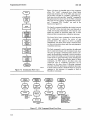
interface connectors, a 50-pin connector (J2) for
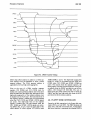
interfacing standard-sized drives and a 34-pin connector (Jl) for interfacing mini-sized drives. Figure
2-4 depicts a typical four-drive system.
~16.
CONTROLLER INTERFACE
SIGNALS
The individual pin assignments for the J2 and J 1
drive interface connectors are given in tables 2-8 and
2-9, respectively. Table 2-10 describes the individual
signal functions.
Table 2-7. Auxiliary Port Jumper Matrix
Jumper Auxiliary Port
Assignment
Post
E11
E9
E7
E2
Bit 0
Bit 1
Bit 2
Bit3
Jumper Interface Connector
Post
Pin Assignment
E10
E8
E6
J1-2, J2-8
J1-4, J2-12
J1-16*, J2-16
*J1-16 is defined as the MOTOR ON 1 signal pin
on the Shugart drive interface.
2-17. DRIVE INTERFACE AC
CHARACTERISTICS
The drive interface ac timing characteristics are
shown in the following timine> diagrams (figures 2-5
through 2-7); the individual timing values are given in
table 2-11.
2-18. DRIVE INTERFACE DC
CHARACTERISTICS
2-15. DRIVE INTERFACING
The iSBC 208 controller can interface up to four
single- or double-sided, standard 8-inch or 5 V4-inch
mini-sized drives. The controller includes two drive
The drive interface de signal characteristics are given
in table 2-12. Note that all controller output signals
are open collector and that all input signals are terminated on the controller with 220/330 ohm resistor
networks.
2-11
Preparation for Use
iSBC 208
Figure 2-4. Typical Four-Drive System (Standard-Sized Drives)
2-12
143078-4
Preparation for Use
iSBC 208
Table 2-8. 12 Interface Connector Pin Assignments
Pin
Assignment
Signal
Pin
Assignment
Signal
2
4
6
8
10
12
14
16
18
20
22
24
26
LOW CURRENT I
HEAD LOAD 21
HEAD LOAD31
Spare
TWOSIDEDI
Spare
SIDE SELECT I
Spare
HEAD LOAD 01
INDEXI
READY I
HEAD LOAD11
DRIVE SELECT 01
28
30
32
34
36
38
40
42
44
46
48
50
DRIVE SELECT 11
DRIVE SELECT 21
DRIVE SELECT 31
DIRECTION I
STEPI
WRITE DATAl
WRITEGATEI
TRACK 01
WRITE PROTECT I
READ DATAl
FAULTI
FAULTRESETI
Note that all odd-numbered pins are connected to logic ground.
Table 2-9. 11 Interface Connector Pin Assignments
Pin
Assignment
Signal
2
4
6
8
10
12
14
16
18
Spare
Spare
READY I
INDEXI
DRIVE SELECT 01
DRIVE SELECT 11
DRIVE SELECT 21
Spare
DIRECTION I
Pin
Assignment
Signal
20
22
24
26
28
30
32
34
STEPI
WRITE DATAl
WRITEGATEI
TRACKOI
WRITE PROTECT I
READ DATAl
SIDE SELECT I
TWOSIDEDI
Note that all odd-numbered pins are connected to.iogic ground.
2-13
Preparation for Use
iSBC 208
Table 2-10. Interface Connector Signal Functions
Signal
Function
LOW CURRENT/
A low-state active output signal used to select low write current compensation circuitry
available in some drives. This signal is enabled during read/write operations and is active (low)
when the track address is 43 or greater. Note that a factory-installed jumper link is used to
route this signal to pin 2 of connector J2.
HEAD LOAD2/
An optional (jumper selectable) low-state active output signal used to load the read/write head
in drive 2. When the head is initially loaded, the controller provides a programmed delay (head
load time) prior to initiating any read/write operation. Following a read/write operation, the
controller delays inactivating the HEAD LOAD 2/ signal until the programmed head unload time
and the one-second fixed delay intElrvals time out. Note that a jumper link must be installed to
route the HEAD LOAD 2/ signal to theJ2 interface connector.
HEAD LOAD3/
An optional low-state active output signal that is functionally identical to HEAD LOAD 2/ except
routed to drive 3.
TWO SIDED/
A low-state active status input signal that indicates the installation of a double-sided diskette
within the drive. Note that a factory-installed jumper link is used to route this signal into the
controller from drive interface connectors J2 and J1, and that this signal is only examined during the Sense Drive Status command.
SIDE SELECT /
An output control signal that selects one side of a double-sided drive. When SIDE SELECT is
low, read/write qperations are performed on side 1 of the drive.
HEAD LOADO/
A low-state active output signal used to load the read/write head in drive O. When configured at
the factory, this signal is the only HEAD LOAD/ signal available on interface connector J2
(common HEAD LOAD/ signal for all drives interfaced), and the additional one-second head
unload delay is not used.
INDEX/
A low-state active input pulse that is coincident with the detection of the index hole in the
diskette (indicates the logical beginning of a track).
READY/
A low-state active input signal indicating that the drive is ready to perform an operation. The
qualifications for READY/are drive dependent and usually include diskette in place, door
closed and diskette rpm at specified speed. The controller uses a common READY / input and
requires that the drives interfaced provide a gated READY / output when individually selected.
HEAD LOAD 1/
An optional low-state active output Signal that is functionally identical to HEAD LOAD 2/ except
routed to drive 1.
DRIVE SELECT 0/
DRIVE SELECT 1/
DRIVE SELECT 2/
DRIVE SELECT 3/
Individual low-state active output signals for selecting the individual drives interfaced. Note
that a DRIVE SELECT 3/ signal is not included on the J1 interface connector and that when
interfacing four mini drives, this signal must be connected to one of the jumper posts
associated with an unassigned pin of connector J1.
DIRECTION/
An output control signal that specifies the direction in which the drive's read/write head is
stepped. This signal is only enablod during seek operations and when at a logic low level,
causes the head to be stepped toward the spindle (step in).
STEP/
A low-state active output pulse that causes the drive to move (step) the read/write head one
track position. The direction that the head is stepped is determined by the state of the
DIRECTION/ output Signal. Like thl~ DIRECTION/ signal, STEP/ is only enabled during seek
operations.
WRITE DATA/
The serial data/clock composite write signal to the drive. The high-to-Iow-going transition of
this signal indicates a bit to be written on the diskette.
WRITE GATE/
A low-state active control signal that is used to enable the drive's write electronics (allowing
data to be written on the diskette). When this signal is in its inactive state, the write electronics
are disabled, and the drive reads data from the diskette.
TRACK 0/
A low-state active input status signal that indicates the drive's read/write head currently is
positioned over track O. Note that this signal is only examined during a seek or recalibrate
operation.
WRITE PROTECT /
A low-state active input status signal that indicates the installation of a write-protected diskette
in the drive. Note that this signal is only examined during a write or format operation.
READ DATA/
The composite (unseparated) data and clock input signal generated by the drive during a
diskette read operation. A high-to-Iow-going transition indicates a clock or data "one" bit.
FAULT/
An optional low-state active input signal that indicates a write fault condition within the drive.
This signal is only examined durin!l read/write operations and requires the installation of a
jumper link to route the signal into the controller from the J2 interface connector.
FAULT RESET/
A low-state active output control Signal that is used to reset fault detection logic optional in
some drives. This signal is automatically generated at the beginning of every read/write
operation and requires the installation of a jumper link to route the Signal to the J2 interface
connector.
2-14
iSBC 208
Preparation for Use
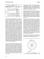
DRIVE SELECT /
DIRECTION/
STEP/
Figure 2-5. Seek Timing
FIRST OPPORTUNITY
\
LAST BYTE
READ OR WRITTEN
TOREjDATA
HEAD LOAD/
ss
F-tHLD---1
143078-5
~
rtHlll-
Figure 2-6. Head Load Timing
CLOCK
+
WRITE DATA/
143078-6
CLOCK
+
~-''''~ "'W ~
Figure 2-7. Write Data Timing
143078-7
2-15
iSBC208
Preparation for Use
Table 2-11. Drive Interface AC Timing Characteristics
Standard 8-inch Drive
Symbol
51!4-inch Mini Drive
Parameter
Units
Minimum
Maximum
Typical
Minimum
Typical
Maximum
Seek Timing
19
38
IlS
DRIVE SELECTI Hold
Time from STEPI
5
10
Ils
tDS
DIRECTION I to STEP I
Setup Time
1
2
Ils
tSD
DIRECTION I Hold
Time from STEPI
24
48
IlS
tSCY
STEP I Cycle Time
1
tspw
STEPI Pulse Width
5
tDSD
DRIVE SELECT I to
DIRECTIONI Setup
Time
tSDS
2
16
32
ms
10
Ils
Head Load Timing
tHLD
Head Load Time
tHUL
Head Unload Time
tHUT
Head Unload
Time-Out (Optional)
2
254
4
508
ms
16
240
32
480
ms
1
1
s
Write Data Timing
tHBC
Half Bit Cell
1 or 2*
2 or 4*
IlS
tFBC
Full Bit Cell
2 or 4*
4 or 8*
tDPW
Data Pulse Width
Ils
ns
200
200
250
250
*FM Mode Values.
Table 2-12. Drive Interface DC Characteristics
Current Loa~
Current Drive
Signal
IOL
IOH
IlL
IIH
48mA
- 25OIlA
-
-
READY/, INDEXI, READ DATAl
-
-O.8mA
40llA
WRITE PROTECT I, TWO SIDED/,
FAULT I, TRACK 01
-
-
-O.2mA
20llA
All Output Signals*
* Auxiliary port output signals have an additional 10k ohm pullup resistor to V cc.
2-16
iSBC 208
Preparation for Use
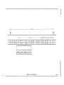
2-19. DRIVE CABLING
I/O interface cable, the cable ends are fitted with the
appropriate mating connectors, and when interfacing
multiple drives, additional drive mating connectors
are inserted directly into the cable to form a daisychain cable. The recommended maximum cable
length between the controller and the (last) drive is 10
feet (3 meters); consult the drive manufacturer's
specifications for additional limitations. Figure 2-8
illustrates a typical daisy-chain flat ribbon cable
designed to interface two standard-sized drives.
The controller uses two drive interface connectors, a
34-pin connector for interfacing mini-sized drives
(J 1) and a 50-pin connector for interfacing standardsized drives (2). Each interface connector can interface up to four drives using a daisy-chain technique.
Since most drives compatible with the controller
follow the Shugart flexible disk drive interface
requirements, flat ribbon cable and mass-termination
type connectors are recommended for cable fabrication. (A number of the individual drive interface
signal pin assignments can be altered or defined by
jumpers on the controller board.) To fabricate the
Table 2-13 lists compatible controller mating connectors and cable. Refer to the drive manufacturer's documentation for the required drive mating
connectors.
Table 2-13. Mating Connectors
Controller
Connector
Mating
Connector
J1
3M 3414-7034 or
T&BI Ansley 609-3401 M
3M ]365/34
T&BI Ansley 171-34
Spectra-Strip (twisted pair)
455-248-34
J2
3M 3425-7050 or
T&BI Ansley 609-5001 M
3M 3365/50
T&B/Ansley 171-50
Spectra-Strip (twisted pair)
455-248-50
,
Cable
[CONTROLLER MATING CONNECTOR
3M 3425-7050 OR EQUIVALENT
F=
r-I!!!!!!!!!!!!!==I~
ff
--=--.-..-.~~I
===
====
~
. --
==
II
-T
DRIVE MATING CONNECTORS-J
(SEE DRIVE MANUFACTURER'S
DOCUMENTATION)
- - - - - 1 0 FEET (MAXIMUM)
Figure 2-8. Flat-Ribbon I/O Interface Cable
143078-8
2-17
iSBC20B
Preparation for Use
2-20. DRIVE MODIFICATIONS
The following subsections define the general drive
modifications that may be necessary to ensure proper
interface with the controller. Detailed information is
included in the drive manufacturer's documentation.
HEAD LOADI (common only)
LOW CURRENT I (if used)
FAULT RESET I (if used)
MOTOR ONI (if used; common only)
2-25. DRIVE NUMBERING
2-21. READY LOGIC
Most standard-sized drives compatible with the controller provide a ready indication to the controller
only when the drive is selected. If the drive provides
an ungated READY I output (generally referred to as
radial ready), the drive must be modified to condition the drive's READY I output with DRIVE
SELECT I. Most mini-sized drives do not provide a
ready indication. Accordingly, when interfacing
drives that do not provide a READY I output, make
sure that the controller's READY I input is permanently enabled with the installation of a jumper
link between jumper posts E17 and E19 as described
in table 2-6.
2-22. MOTOR-ON CONTROL
The MOTOR ONI control output for mini-sized
drives must be enabled prior to drive selection to
allow time for the drive to reach operating speed
before an operation is initiated. Accordingly, the
MOTOR ONI input to the drive must not be gated
with DRIVE SELECT I. Note that this restriction
applies when using either a common MOTOR ONI
signal or a radial MOTOR ONI signal in multipledrive configurations.
2-23. RADIAL HEAD LOAD
As an option, the controller can be configured to
provide individual (radial) HEAD LOADI outputs.
When this option is used, the individual HEAD
LOADI signals must not Qe gated with their
associated DRIVE SELECT I signal within the drive.
2-24. DRIVE TERMINATION
When two or more drives are interfaced (daisychained) to the controller, the termination
resistors/networks on the following common drive
input signal lines must be removed from all but the
last physical drive on the cable:
DIRECTION I
STEPI
WRITE DATAl
WRITEGATEI
2-18
When interfacing multiple drives, each drive must be
assigned a unique drive unit number. Depending on
the manufacturer, internal drive unit assignment may
be determined by wire jumper, shorting plug, or
individual switch contacts. Generally, drives are
shipped by their manufacturer configured for singledrive systems (i.e., the drive is assigned unit 0 with
drives numbered 0 through 3 or unit 1 with drives
numbered 1 through 4).
2-26. MULTIPLE DRIVE
PIN ASSIGNMENTS
When interfacing more than one drive, unique pin
assignments for the individual DRIVE SELECT/,
MOTOR ONI (when used in radial configuration),
and radial HEAD LOADI (optional) signal lines
associated with each drive must be provided. The
actual pin assigned will depend on pin availability
based on drive features supported and interface
signal requirements. Note that it may be necessary to
cut traces within the drive in order to reroute the
input signal within the drive. It also may be necessary
to cut traces to omit non-critical drive status signals
(e.g., TWO-SIDEDI or IN USE) in order to provide
additional pin assignments on the interface. Appe:ndix C lists the pin assignments for a number of the
standard- and mini-sized drives compatible with the
controller.
2-27. STEPPER MOTOR POWER
Many drives compatible with the controller support a
power-down feature that allows power to the stepper
motor to be enabled only when the drive is selected.
Since the controller automatically polls all four
possible drives for a change in drive-ready status by
cycling through the DRIVE SELECT I lines, the
power down feature cannot be supported directly
(i.e., power to the stepper motor must not be dependent on drive selection). Note that in addition to the
above restriction, the interval between drive selection
and the generation of the first STEP I pulse is too
short to allow the stepper motor to be enabled by the
DRIVE SELECT I lines. When the stepper motor
power-down featue is to be used, the host processor
must enable and disable the stepper motor through
the controller's auxiliary port.
CHAPTER 3
PROGRAMMING INFORMATION
3-1. INTRODUCTION
This chapter describes the 110 port commands that
are executed by the host processor to convey information to and from the controller's programmable
flexible disk controller (FDC) and DMA controller
(DMAC) circuits and the individual FDC commands
that control all disk operations and the transfer of
data to and from the drive. Additionally, this chapter
contains a description of the diskette formats supported and individual flow charts depicting the
various diskette operations.
All disk operations are defined and initiated by the
host processor through the execution of a series of
110 port commands while the controller is functioning as a bus slave. Once all information required to
define the operation has been received, the controller
functions as a bus master; the controller accesses and
maintains control of the system bus and completes
the specified operation without further intervention
from the host processor. When the operation is complete, the controller reverts to a bus slave; the host
processor must interrogate the controller to determine the outcome of the operation.
To initiate a disk operation, a series of 110 port commands is executed by the host processor. This series
of commands defines the FDC operation to be performed, provides all supplemental information
(parameters) required to perform the operation, and,
if a data transfer to or from the diskette is indicated,
defines the direction of the data transfer, the starting
memory address of the first data byte to be transferred and the I,lUmber of bytes to be transferred.
3-2. 1/0 PORT COMMANDS
Host processor communication with the controller is
accomplished through an 110 port address block as
defined by the least-significant bits of the 110
address. The location of this block (the 110 base
address) in host processor memory must be on a
32-bit boundary (64-bit boundary with iSBX
Multimoduk board installed) and is defined by the
user through a set of jumpers on the controller.
These jumpers correspond to the three mostsignificant bits of an 8-bit 110 address or the eleven
most-significant bits of a 16-bit 110 address (8- or 16bit I/O addressing is user-selectable by an additional
jumper on the controller).
The host processor executes an 110 port read or write
instruction at one of the locations within the 110 port
address block to transfer information either to (110
write) or from (110 read) the controller. Table 3-1
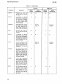
defines the controller's I/O port command set. Note
that a number of the ports can be both read and written while other ports are either read-only or writeonly. Each port command transfers one byte of data;
a number of the 110 port commands require two
data bytes (i.e., the port command must be issued
twice to transfer all data associated with the 110 port
command).
3-3. READ/WRITE DMAC ADDRESS
REGISTERS
The controller's DMAC circuit has four DMA channels of which three channels are available. Each
channel has an identical pair of 16-bit address
registers, a "current-address" register, and a "baseaddress" register (each channel also has an identical
pair of 16-bit word-count registers). Channel 0 is
used by the controller for all diskette data transfers,
Channel 1 is not used, and Channels 2 and 3 are
available for use by an iSBX Multimodule board
installed on the controller.
The Write DMAC Address Register command is used
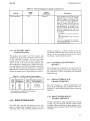
to simultaneously load a channel's current-address
register and base-address register with the memory
address of the first byte to be transferred. (The
Channel 0 current/base address register must be
loaded prior to initiating a diskette read or write
operation.) Since each channel's address registers are
16 bits in length (64K address range), two "write
address register" commands must be executed in
order to load the complete current/base address
registers for any channel. The register byte loaded
(high- or low-order) is determined by the state of the
DMAC's first/last flip-flop. (When the flip-flop is
reset, the associated data byte is written into the Ioworder eight bits of the register; the flip-flop is toggled
with each command so that a second address register
command accesses the "other" byte.) The currentaddress register is incremented with each byte
transferred; the base-address register maintains its
initial value until it is reloaded by a subsequent Write
Address Register command (or until the DMAC or
controller is reset).
The Read DMAC Address Register command reads
the low- or high-order byte of a channel's currentaddress register (a channel's base-address register
3-1
Programming Information
iSBC 208
Table 3-1. I/O Port Controller Commands
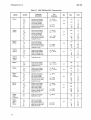
Port
Address
3-2
Mode
Command Function
0
Write
Read
Load OMAC Channel 0 Base and Current Address Regsiters
Read OMAC Channel 0 Current Address Register
1
Write
Read
Load OMAC Channel 0 Base and Current Word Count Registers
Read OMAC Channel 0 Current Word Count Register
2,3
-
4
Write
Read
Load OMAC Channel 2 Base and Current Address Registers
Read OMAC Channel 2 Current Address Register
5
Write
Read
Load OMAC Channel 2 Base and Current Word Count Registers
Read OMAC Channel 2 Current Word Count Register
6
Write
Read
Load OMAC Channel 3 Base and Current Jlddress Registers
Read OMAC Channel 3 Current Address Register
7
Write
Read
Load OMAC Channel 3 Base and Current Word Count Registers
Read OMAC Channel 3 Current Word Count Register
8
Write
Read
Load OMAC Command Register
Read OMAC Status Register
9
Write
Load OMAC Request Register
OA
Write
Set/Reset OMAC Mask Register
OB
Write
Load OMAC Mode Register
OC
Write
Clear OMAC First/Last Flip-Flop
00
Write
OMAC Master Clear
OE
-
OF
Write
Load OMAC Mask Register
10
Read
Read FOC Status Register
11
Write
Read
Load FOC Data Register
Read FOC Data Register
12
Write
Read
Load Controller Auxiliary Port
Poll Interrupt Status
13
Write
Controller Reset
14
Write
Load Controller Low-Byte Segment Address Register
15
Write
Load Controller High-Byte Segment Address Regist.er
16-1F
-
Not Used
20-2F
-
Reserved for iSBX Multimodule Board (see Appendix B)
Reserved
Reserved
iSBC 208
cannot be read). The current-address register byte'
accessed is determined by the state of the DMAC's
first/last flip-flop as previously described.
3-4. READ/WRITE DMAC WORD
COUNT REGISTERS
Like the DMAC address registers, each DMA channel also has an identical pair of 16-bit word-count
registers, a "current word-count register" and a
"base word-count register." The channel 0 wordcount registers are used to specify the number of
bytes to be transferred during a diskette read or write
operation. The channel 1 word-count registers are
not used, and the word-count registers for channels 2
and 3 are dedicated to DMA functions associated
with a Multimodule board.
The Write DMAC Word Count Register command is
used to simultaneously load a channel's current and
base word-count registers with the number of bytes
to be transferred during a subsequent DMA operation. Since the word-count registers are 16-bits in
length, two commands must be executed to load both
halves of the registers. As described in section 3-3,
the register half loaded (low- or high-order) is determined by the state of the DMAC's first/last flip-flop.
The actual count loaded is a binary value that is one
less than the number of bytes to be transferred (i.e.,
the register value 01 FFH transfers 512 bytes). During
the subsequent DMA transfer, the current wordcount register is decremented with each byte transferred; the base word-count register maintains its
initially-loaded value until it is reloaded by a subsequent Write Word Count Register command or until
either the DMAC or controller is reset. When the
word count decrements to zero, the DMA transfer is
stopped and the corresponding TC (terminal count)
bit in the DMAC status register is set.
The Read DMAC Word Count Register command
reads the low- or high-order byte of a channel's
current word-count register (a channel's base wordcount register cannot be read). The current wordcount register byte accessed is determined by the state
of the DMAC's first/last flip-flop.
Programming Information
are applicable to the controller; the remaining bits
select functions that are not supported and,
accordingly, must always be set to zero.
MEMORY·TO·MEMORY DISABLE
GHANNEL 0 ADDRESS HOLD DISABLE
L-------l 0 CONTROLLER ENABLE
'1 CONTROLLER DISABLE
' - - - - - NORMAL TIMING
' - -_ _ _~ (I FIXED PRIORITY
11 ROTATING PRIORITY
~----- I.ATE WRITE SELECTION
~------ [)REQ SENSE ACTIVE HIGH
~------- [)ACK SENSE ACTIVE LOW
Bit 2:
Controller Enable/Disable. This bit, when
set to one, prevents all DMA channels from
responding to data transfer requests. Normally, this bit is always set to zero to enable
the DMAC. When multiple DMA channels
are used and a non-essential DMA request
from the iSBX Multimodule board could
interrupt the programming of channel 0, the
DMAC could be disabled while it is being
programmed and then enabled by a subsequent Write DMAC Command Register
command after it has been programmed.
Bit 4:
Fixed/Rotating Priority. This bit, when set
to zero, selects fixed priority (channel 0 has
the highest priority, channel 3 has the lowest
priority) and when set to one, selects rotating
priority (each channel is granted highest
priority on a rotational scheme).
Note that when programming the command register,
an aU-zero byte enables the DMAC and gives the disk
controller (channel 0) the highest priority. The command register is cleared by a DMAC master clear or
controller reset.
3-6. READ DMAC STATUS REGISTER
COMMAND
The Read DMAC Status Register command accesses
an 8-bit status byte that identifies the DMA channels
that have reached terminal count or that have a pending DMA request.
3-5. WRITE DMAC COMMAND
REGISTER
The Write DMAC Command Register command
loads an 8-bit byte into the DMAC's command
register to define the operating characteristics of the
DMAC. The functions of the individual bits in the
command register are defined in the following
diagram. Note that only two bits within the register
'---'----'-----'------'-------L -_ _ _ _ _ _ _
CftANNELOTC
CHANNEL1 TC
CflANNEL2TC
CflANNEL3 TC
CHANNEL 0 DMA REQUEST
CHANNEL1 DMA REQUEST
CflANNEL2 DMA REQUEST
CflANNEL3 DMA REQUEST
3-3
iSBC208
Programming Information
Bits 0 through 3 are set when their corresponding
channel has reached terminal count (i.e., when the
channel's current word count register decrements to
zero). Since DMA channell is not used, bit 1 always
is zero. Bits 2 and 3 are associated with an iSBX
Multimodule board and indicate a terminal count
condition on channels 2 and 3. Note that if external
EOP (End of Process) logic is implemented on the
iSBX Multimodule board, the generation of an external EOP signal sets the active channel's TC bit
irrespective of the current word count.
3-8. SET IRESET DMAC MASK
REGISTER
The Set/Reset DMAC Mask Register command is
used to reset (or set) individual bits within the
DMAC's internal 4-bit mask register. Each DMAC
channel has an associated mask bit within the register
that, when reset, enables the channel's DREQ (DMA
Request) input and, when set, disables (masks) the
DREQ input.
76543210
Bits 4 through 7 are set when their corresponding
channel requests DMA service (DMAC's DREQ
input activated or corresponding bit in the request
register set). Again, since DMA channell is not used,
bit 5 always is zero, and bits 6 and 7 indicate DMA
requests originating from an iSBX Multimodule
board.
The TC bits in the status register are cleared
whenever the register is read by a DMAC master
clear or by a controller reset.
3-7. WRITE DMAC REQUEST REGISTER
The Write DMAC Request Register command is used
with DMAC channels 2 and 3 (the iSBX Multimodule
board channels) to allow DMA requests to be initiated by the host processor. The command only can
be used when the selected channel is operated in the
"block transfer mode" (see section 3-9); the controller's DMA channel (channel 0) operates in either
the "single transfer mode" or the "demand transfer
mode" and does not use the Write DMAC Request
Register command.
The data byte associated with the Write DMAC
Request Register command sets or resets a channel's
associated request bit within the DMAC's internal 4bit request register.
DON'T CARE
L{
00 SELECT CHANNEL 0
01SELECTCHANNEL1
10 SELECT CHANNEL 2
11 SELECTCHANNEL3
' - - _ - { 0 RESET MASK BIT
1 SET MASK BIT
Prior to a DREQ-initiated DMA transfer, the channel's mask bit must be reset to enable recognition of
the DREQ input. When the transfer is complete (terminal count reached or external EOP applied) and
the channel is not programmed to autoinitialize, the
channel's mask bit is automatically set (disabling
DREQ) and must be reset prior to a subsequent
DMA transfer. All four bits of the mask register are
set (disabling the DREQ inputs) by a DMAC master
clear or controller reset. Additionally, all four bits
can be set/reset by a single Write DMAC Mask
Register command (see section 3-12).
3-9. WRITE DMAC MODE REGISTER
The Write DMAC Mode Register command is used
to define the operating mode characteristics for each
DMA channel. Each channel has an internal 6-bit
mode register; the high-order six bits of the
associated data byte are written int'o the mode
register addressed by the two low-order bits.
76543210
DON'T CARE
L{
00 SELECT CHANNEL 0
01 SELECT CHANNEL 1
. 10 SELECT CHANNEL 2
11 SELECT CHANNEL3
' - - _ - { 0 RESET REQUEST BIT
1 SET REQUEST BIT
The individual channel request bits are non-maskable
and are subject to channel prioritization (fixed or
rotating). Each request bit is individually set or reset
according to the state of bit 2 and, when onc.e set
within the register, is cleared when the corresponding
channel reaches terminal count or when an external
EOP signal is applied. The entire request register is
cleared by a DMAC master clear or controller reset.
3-4
r1
9°OCHANNECO""CT
MCHANNEL1SELECT
10 CHANNEL 2 SELECT
1'1 CHANNEL 3 SELECT
00 VERIFY TRANSFER
01 WRITE TRANSFER
10 READ TRANSFER
11 (ILLEGAL)
' - - - - - - 1 0 AUTOINITIALIZE DISABLE
1 AUTOINITIALIZE ENABLE
'--_ _ _ _~ 0 ADDRESS INCREMENT
1 ADDRESS DECREMENT
00 DEMAND MODE
'--_ _ _ _ _---{ 01 SINGLE MODE
10 BLOCK MODE
11 (Illegal)
iSBC 208
Verify Transfer. The verify transfer mode is not
used by the controller; this mode may be used by an
iSBX Multimodule board.
Write Transfer. The write transfer mode programs
the selected DMA channel to transfer data from the
110 device to host memory. This mode must be
selected to read data from the diskette (i.e., the data
read from the diskette is written into host memory).
Read Transfer. The read transfer mode programs
the selected DMA channel to transfer data from host
memory to the 110 device. This mode must be
selected to write data on the diskette (i.e., the data
read from host memory is written onto the diskette).
Autoinitialize. The autoinitialize enable/disable bit
is used to control a channel's autoinitialization function. When this bit is set (1), the autoinitialize mode
is enabled, and the current word-count and current
address register values are automatically restored
from the corresponding base registers when the DMA
transfer is complete (terminal count or EOP). The
mask bit is not set when the autoinitialize mode is
enabled, and the channel is prepared to perform a
subsequent DMA transfer without reprogramming
the DMAC. Note that for most controller applications, the autoinitalize mode is not used.
Address Increment/Decrement. The address increment/decrement bit determines the sequence in
which memory addresses are generated. When this
bit is reset (0), the memory address in the current
address register is incremented with each byte
transferred. Conversely, when the address increment/decrement bit is set (I), the memory address in
the current address register is decremented with each
byte transferred. Note that for most controller
applications, the address increment mode is used.
Demand Mode. In the demand transfer mode the
channel data transfer is initiated by DREQ. The
channel continues to transfer data until DREQ goes
inactive or until either a terminal count condition is
reached or an external EOP is received. If DREQ is
held active throughout the entire transfer, the channel maintains bus access until the transfer is complete. The controller (DMAC channel 0) can use the
demand transfer mode; however, since the DREQ
input from the FDC goes inactive following each byte
transferred, the channel releases the bus after each
byte transferred.
Single Transfer Mode. In single transfer mode, the
channel performs a sequence of single byte transfers
(the channel releases the bus after each byte transferred) until the transfer is complete (terminal count
reached or external EOP applied). DREQ must be
held active by the 110 device until DACK is received.
Programming Information
Unlike the demand mode, if DREQ is held active
throughout the entire transfer, the bus is released
with each byte transferred. The controller normally
uses the single transfer mode for all DMA data
transfers.
NOTE
Since both the demand and single transfer
modes used by the controller release the bus
with each byte transferred, the controller
should be given "high bus priority" to prevent interruptions in the DMA transfer.
Block Mode. In block transfer mode the channel
data transfer again is initiated by DREQ. The
transfers continue, irrespective of the state of DREQ,
until terminal count is reached or an external EOP is
applied. (DREQ must be held active until DACK is
received.) The controller does not support operation
in the block transfer mode; this mode may be used by
an iSBX Multimodule board.
3-10. CLEAR DMAC FIRST/LAST
FLIP-FLOP
The Clear DMAC First/Last Flip-Flop command
initializes the DMAC's int'ernal first/last flip-flop so
that the next byte written to or read from the 16-bit
address or word-count registers is the low-order byte.
The flip-flop is toggled with each register access so
that a second register read or write command
accesses the high-order byte. The first/last flip-flop
also is initialized (to access the low-order register
byte) by a DMAC master clear or controller reset.
Note that the Clear DMAC First/Last Flip-Flop
command does not require a specific bit pattern in
the associated command data byte.
3-11. DMACMASTERCLEAR
The DMAC Master Clear command clears the
DMAC's command, status, request, and temporary
registers to zero, initializf!s the first/last flip-flop,
and sets the four channel mask bits in ·the mask
register to disable all DMA requests «(.e., the DMAC
is placed in an idle state). Note that the DMAC
Master Clear command dOf!S not require a specific bit
pattern in the associated command data byte.
3-12. WRITE DMAC MASK REGISTER
The Write DMAC Mask Register command allows
all four bits of the DMAC's mask register to be
written with a single command.
3-5
Programming Information
7
6
543
2
1
iSBC 208
0
o CLEAR CHANNEL 0 MASK BIT
NON-DMA MODE. This bit only is applicable in
systems that do not support OMA tranfers and is
irrelevant to the controller.
1 SET CHANNEL 0 MASK BIT
o CLEAR CHANNELl MASK BIT
1 SET CHANNEL 1 MASK BIT
o CLEAR CHAIIINEL2 MASK BIT
1 SET CHANNEl 2 MASK BIT
L - -_ _ _
0 CLEAR CHANNEL3 MASK BIT
1 SETCHANNEL3MASK BIT
Like the Set/Reset OMAC Mask Register command,
clearing a channel's mask bit enables recognition of
the associated OREQ input, and setting a channel's
mask bit disables (masks) the associated OREQ
input. Again, a OMAC master clear or controller
reset sets all four mask register bits (disabling the
OREQ inputs).
3-13. READ FDC STATUS REGISTER
The Read FOC Status Register command accesses the
FOC's main status register. The individual status
register bits are as follows:
76543210
FDDOBUSY
FDD 1 BUSY
L-...._ _ FDD 2 BUSY
L--_ _ _ FDD 3 BUSY
' - - - - - - FDC BUSY
L - -_ _ _ _ _ NON-DMA MODE
L - -_ _ _ _ _ _ DATAINPUT/OUTPUT
' - - - - - - - - - - REQUEST FOR MASTER
FDD 0 BUSY. This bit, when set (1), indicates
that drive 0 is in the process of performing a seek
operation.
FDD 1 BUSY. This bit, when set, indicates
that drive 1 is in the process of performing a seek
operation.
FDD 2 BUSY. This bit, when set, indicates
that drive 2 is in the process of performing a seek
operation.
DATA INPUT/OUTPUT. The data input/output
(DIO) bit indicates the direction of the transfer
between the FOC's data register and the host processor. When this bit is set, the direction of the
transfer is from the FOC to the host processor, and
when this bit is reset, the direction of the transfer is
from the host processor to the FOC.
REQUEST FOR MASTER. The request for master
(RQM) bit, when set, indicates that the FOC's data
register is ready to presell1t a byte to or accept a byte
from the host processor.
The host processor can read the main status register
at any time and should use the 010 and RQM status
bits to perform a "handshaking" function with the
FOC when transferring data to or from the FOC's
data register. Figure 3-\ shows the status register
timing.
Note that like any microprocessor, the FOC requires
a finite amount of time to update its RQM status bit
between byte transfers to or from the data register.
The sample PL/M and assembly language drivers in
Appendix A illustrate typical wait subroutines that
must be inserted between successive byte transfers to
or from the FOC's data register.
3-14. READ/WRITE FDC DATA
REGISTER
The Read and Write FOC Oata Register commands
are used to write command and parameter bytes to
the FOC in order to specify the operation to be performed (referred to as the "command phase") and to
read status bytes from the FOC following the operation (referred to as the "result phase"). Ouring the
command and result phases, the 8-bit data register is
actually a series of 8-bit registers in a stack. Each
register is accessed in sequence;. the number of
registers accessed and th(! individual register contents
are defined by the specific disk command (refer to
the FOC command descriptions in sections 3-20
through 3-32).
FDD 3 BUSY. This bit, when set, indicates
that drive 3 is in the process of performing a seek
operation.
3-15. WRITE CONTROLLER AUXILIARY
PORT
FDC BUSY. This bit, when set, indicates that the
FOC is in the command execution phase (i.e., the
FOC is in the process Of performing a diskette read
or write operation).
The Write Controller Auxiliary Port command is
used to set or clear individual bits within the controller's auxiliary port. The four low-order port bits
are dedicated to auxiliary drive control functions
3-6
iSBC208
Programming Information
OUT OF FDC AND INTO PROCESSOR
DATA IN-OUT
(010)
OUT OF PROCESSOR AND INTO FDC
REOUEST
FOR MASTER
(ROM)
LJ
I
I
uI
NOTES:
I I
A
A
B
-
C
-
o -
I I
B
II
I I
B
I I I II
u
I I
I I
A
in
I I
RD
I
I
I
I
I
WR
I
I
READY
A
I
IY II
I I I II
C
0
C
0
B
A
I
DATA REGISTER READY TO BE WRITTEN INTO BY HOST PROCESSOR
DATA REGISTER NOT READY TO BE WRITTEN INTO BY HOST
PROCESSOR
DATA REGISTER READY FOR NEXT DATA BYTE TO BE READ BY THE
HOST PROCESSOR
DATA REGISTER NOT READY FOR NEXT DATA BYTE TO BE READ BY
THE HOST PROCESSOR
Figure 3-1. Main Status Register Timing
(jumper links are required to connect the desired port
bit to an available pin on the drive interface connectors; see section 2-14). The most common application
for these bits is the "Motor-On" control function for
mini-sized drives.
The four high-order bits of the auxiliary port are the
AORI4 through AOR17 address bits that are used to
extend the OMA addressing capability of the controller to 16 megabytes (24-bit addressing). These bits
are set prior to initiating a diskette read or write
operation to define the specific I-megabyte page of
memory to be accessed.
143078-9
when interrupts are disabled to poll the controller
(and iSBX Multimodule board) in order to determine
when an operation has been completed. A bit set in
the status byte returned indicates a pending interrupt.
7
6
5
4
321
0
L...-_ _
GONTROLLER INTERRUPT
MULTIMODULE BOARD
INTERRUPTO
MULTIMODULE BOARD
INTERRUPT 1
3-17. CONTROLLER RESET
3-16. POLL INTERRUPT STATUS
The Poll Interrupt Status command presents the
interrupt status of the controller and the two interrupt status lines dedicated to the iSBX Multimodule
board. This command is used by the host processor
The Controller Reset command is the software reset
for the controller. This command clears the controller's auxiliary port and segment address register,
provides a reset signal to the iSBX Multimodule
board and initializes the bus controller (releases the
bus), the OMAC (clears the internal registers and
masks the OREQ inputs), and the FOC (places the
FOC in an idle state and disables the output control
lines to the diskette drive). Following reset, the
controller is in an idle stat~:. Note that the Controller
Reset command does not require a specific bit pattern in the associated command data byte.
3-7
Programming Information
iSBC 208
3-18. WRITE CONTROLLER LOW- AND
HIGH-BYTE SEGMENT ADDRESS
REGISTERS
The Write Controller Low- and High-Byte Address
Registers commands are required when the controller
uses 20-bit addressing (memory address range from 0
to OFFFFFH). These commands are issued prior to
initiating a diskette read or write operation to specify
the 16-bit segment address. The data byte loaded into
the low-order half of the register is the A4 through
All address bits, and the data byte loaded into the
high-order half of the register is the A12 through A19
address bits.
76543210
IA111A101 A91 Asl A71 A61 Asl A41
LOW-ORDER SEGMENT ADDRESS
7
6
S
4
3
2
1
0
IA191 A1SIA17IA161 A1SlA141A131A121
HIGH-ORDER SEGMENT ADDRESS
During the subsequent DMA transfer, the segment
address is combined with the DMAC's current
address to form a 20-bit "effective" address. As
shown in figure 3-2, the segment address value is offset by four bit positions and added to the current
address value.
15
The segment address register is reset (to zero) by the
Reset Controller command.
3-19. DISKETTE ORGANIZATION
The controller is compatible with two physical sizes
of diskettes: a single- or double-sided, standard 8inch diskette that typically consists of 77 tracks and a
single- or double-sided 5 Y4 -inch mini diskette that
typically consists of 35 tracks. Note that the term
"cylinder" is used with double-sided drives to
indicate the set of two tracks at a given head position.
The tracks are numbered sequentially (beginning at
the outermost track) from 0 to 76 (standard size) or
from 0 to 34 (mini size). Each track, in turn, is
divided into sections or "sectors." The number of
sectors on each track and the number of bytes per
sector are program-determined ("soft sectoring")
and are established when the track is formatted. The
controller is programmed to operate in either the
single-density (FM) format or the double-density
(MFM) format. Figure 3-3 and table 3-2 describe the
track and sector formats for both single- and doubledensity recording, and table 3-3 defines the recording
capacities for both the standard 8-inch and 5 Y4 -inch
mini drives.
o
Figure 3-2. 20-Bit Addressing
3-8
143078-10
1il
O;j
(j
~
00
I_
1 TRACK
J
I~
1-
1 SECTOR
-,
-I-
NEXT SECTOR-j
r
fL
LAST SECTORl
GAP3i GAP4B
r--------l
A
..."tIo
~
~
i3
i3
S·
--
OQ
:l
o...
i3
w
\0
Figure 3-3. Track Format
....
~
143078-11
o·
:l
Programming Information
iSBC208
Table 3-2. Track Format
FM Format
Designation
MFM Format
Description
Number
of Bytes
GAP4A
Preamble gap; written by
the FOC when the track is
formatted.
40
FF
80
4E
SYNC4
A sequence of all-zero
bytes used to synchronize
the controller's data separa"
tion logic prior to reading
the index address mark;
written by the FOC when the
track is formatted.
6
00
12
00
INOEXAM
Index address mark. Unique
data pattern that identifies
the logical beginning of a
track; written by the FOC
when the track is formatted.
GAP1
Post index gap; written by
the FOC when the track is
formatted.
26
FF
50
4E
SYNC1
A sequence of all-zero
bytes used to synchronize
the controller's data separation logic prior to reading an
10 field address mark; written by the FOC when the
track is formatted.
6
00
12
00
lOAM
10 field address mark.
Unique data pattern that
identifies the beginning of a
sector 10 field; written by
the FOC when the track is
formatted.
10 FIELO
Four bytes used to uniquely
identify each sector on a
diskette by track address,
side, sector number and
sector size; these bytes are
supplied to the FOC by the
program (format table) and
written in the 10 field when
the track is formatted.
4
10CRC
A 16-bit cyclic redundancy
check character derived by
the FCO from the 10 address
mark and the four 10 field
bytes and written immediately following the 10 field
when the track is formatted.
2
GAP2
Post 10 field gap; written by
the FOC when the track is
formatted. Ouring sector
write operations, the controller switches the drive
electronics from read to
write during the post 10 field
gap interval.
11
3-10
Pattern
(Hexadecimal)
Oata=FC
Clock=07
Oata=FE
Clock=C7
Number
of Bytes
4
Pattern
(Hexadecimal)
3 Bytes C2,
1 Byte FC
4
3 Bytes A1,
1 Byte FE
4
2
FF
22
4E
iSBC208
Programming Information
Table 3-2. Track Format (Cont'd.)
FM Format
Designation
Description
Number
of Bytes
Pattern
(Hexadecimal)
MFM Format
Number
of Bytes
Pattern
(Hexadecimal)
SYNC 2
A sequence of all-zero
bytes used to synchronize
the controller's data separation logic prior to reading a
data field address mark.
These sync bytes are rewritten by the FDC during every
sector write operation.
DATA AM
Data field address mark.
Unique data pattern that
identifies the beginning of a
sector's data field; the data
field address mark is written
by the FDC each time the
sector is written. Note that
data pattern F8 (deleted
data mark) is used in place
of FB to identify a deleted
sector.
DATA FIELD
The sector's data field. The
length of the data field
(number of bytes) is programmable: 128 (singledensity only), 256, 512, 1024,
2048,4096, and 8192 (doubledensity only).
DATACRC
A 16-bit cyclic redundancy
check character derived by
the FDC from the data field
address mark and the data
field bytes and written
immediately following the
data field during sector
write operations. During
subsequent sector read
operations, a second CRC
character is calculated from
the data read and compared
with the CRC character
previously written to verify
data integrity.
GAP3
Post data field gap. A
prog ram-selectable gap
length that separates the
previous sector's data field
from the next sector's ID
field. The gap length
specified is dependent on
the recording format and
sector length (see table
3-10). Note that the gap
length specified differs for
a format command and
read Iwrite commands.
FF
4E
GAP4B
Postamble gap. A variablelength gap that follows the
last sector on a track. This
gap is written by the FDC
when the track is formatted
and extends from the end of
gap 3 to the index pUlse'.
FF
4E
6
00
12
FB
4
2
00
3 Bytes A1,
1 Byte FB
2
3-11
Programming Information
iSBC208
Table 3-3. Recording Capacities
Bytes Per Sector
Sectors
Per
Track
Drive
Size
Standard
8-inch
51f4-inch
mini
Bytes Per Track (Formatted)
Single Density
(FM)
Double Density
(MFM)
Single Density
(FM)
Double Density
(MFM)
26
15
8
4
2
1
128
256
512
1024
2048
4096
256
512
1024
2048
4096
8192
3328
3840
4096
4096
4096
4096
6656
7680
8192
8192
8192
8192
18
16
8
4
2
1
128
128
256
512
1024
2048
256
256
512
1024
2048
4096
2304
2048
2048
2048
2048
2048
4608
4096
4096
4096
4096
4096
3-20. FDC COMMANDS
The FDC is capable of executing 12 unique commands. Of these 12 commands, all but one (the Sense
Interrupt Status command) require a multibyte
transfer from the host processor to initiate command
execution. Following the execution of most commands, the host processor must initiate a multibyte
transfer from the FDC to determine the outcome of
the operation and to terminate the command. Table
3-4 lists the FDC commands and the number of bytes
required to initiate and to terminate the command.
Table 3-4. FOC Commands
Command
Specify
Seek
Read Data
Read Deleted Data
Read ID
Read Track
Write Data
Write Deleted Data
Format Track
Recalibrate
Sense Drive Status
Sense Interrupt Status
Command
Bytes
Result
Bytes
3
3
9
9
2
9
9
9
6
0
0
7
7
7
7
7
7
7
0
1
2
2
2
1
FDC command processing consists of three phases
that are entered in the following sequence:
1.
2.
3-12
Command Phase. The host processor initiates
command processing by writing one or more
bytes to the FDC's data register. Depending on
the command to be executed, up to nine bytes
may be required before the execution phase.can
be entered.
Execution Phase. The operation specified during
the command phase is performed. The execution
phase is entered automatically when the last command byte is received. Since the controller uses
DMA for all data transfers to and from the
diskette, no host IProcessor intervention is
required during the execution phase.
3.
Result Phase. Following command execution,
the FDC enters the result phase. With most commands, the FDC generates an interrupt to inform
the host processor of the completion of the execution phase. To complete the result phase the
host processor must read a series of bytes from
the FDC's data register.
During the command and result phases, the main
status register must be read by the host processor to
determine when the FDC is ready to provide or
accept the next command or result byte to be written
or read from the data register as described in section
3-13. Note that during multibyte transfers to or from
the FDC's data register, a delay interval must be
inserted between each byte read or written to allow
time for the FDC to upda.te the main status register
(see "wait" routines in the sample drivers in
Appendix A).
During the execution phase of commands that
transfer data to or from the diskette, the FDC
generates a DMA request for each byte transferred.
The DMAC responds to the DMA request with a
DMA acknowledge to reset the DMA request. When
the transfer is complete (terminal count received
from the DMAC), the FDIC generates an interrupt to
indicate the beginning of the result phase. When the
host processor reads the first byte from the FDC's
data register (status byte STO), the FDC automatically clears the interrupt. The host processor
must read all of the result bytes to complete the command; the FDC will not accept a new command until
the current command is completed.
Programming Information
iSBC 208
The FDC contains five status registers. The main
status register, as previously mentioned, is read by
the host processor during the command and result
phases. The other four status registers (STO, STl,
ST2 and ST3) are read directly from the FDC's data
register during the result phase. The status registers
presented are determined by the FDC command executed. Table 3-5 defines the contents of the four
result status registers.
The writing and reading of the command and result
bytes to and from the FDC's data register must be
performed in the order shown by the command format tables given in the individual FDC command
descriptions. After the last command byte is written
to the FDC, the execution phase starts automatically.
During the execution phas1e of commands that write
data to or read data from the diskette, the number of
bytes transferred is determined by the word-count
value loaded into the DMAC. The DMAC signals the
FDC when the programmed number of bytes have
been transferred; the FDC then stops the transfer,
interrupts the host processor, and enters the result
phase. When the host processor reads the last result
byte from the FDC's data register, the command is
completed and the FDC is prepared to accept a new
command.
Table 3-6 defines the mnemonics used in the command format tables for the individual commands.
Table 3-5. Result Phase Status Registers
Status Register 0 (STO)
Bit(s)
07,06
Name
Interrupt Code
Symbol
IC
Description
07=0 and 06=0
Normal Termination of Command. Command execution was completed successfully.
07=0 and 06=1
Abnormal Termination of Command. Command execution was
initiated, but was not completed successfully.
07=1 and 06=0
Invalid Command Issued. Command execution was not initiated.
07=1 and 06=1
Ready Change. During command execution the drive went Not
Ready.
05
Seek End
SE
Set (05=1) when the FOC completes execution of a Seek command.
Note that there is no result byte associatHd with a Seek command;
the host processor must issue a Sense Interrupt Status command
to access the STO status byte. When parallel (overlapped) seeks are
performed on multiple drives, this bit is set by the first drive to complete its seek (the drive completing its seek is identified by unit
select bits DO and 01). When performing overlapped seeks, the
main status register must be examined to determine when the other
drives have completed their seeks.
04
Equipment Check
EC
Set when the addressed drive activates its FAULT 1 signal to the
controller or when during execution of a Recalibrate command, a
TRACK 01 signal is not received from the addressed drive after 77
STEPI pulses have been issued. Note tilat if a FAULT 1 signal is
received during command execution, the operation is terminated
immediately.
03
Not Ready
NR
Set when a command that accesses the drive is issued and the
drive is in a not-ready state or when a diskette read or write command, which specifies side 1 of a single-sided drive, is issued. The
command issued is not executed.
02
Head Address
HO
Indicates the state of the head (side selected) when the interrupt
was generated (0 = side 0, 1 = side 1).
01,00
Unit Select
US
Indicates the drive unit number of the drive addressed when the
interrupt was generated.
01 =0,00=0 = DRIVE
01=0,00=1 = DRIVE
01=1,00=0 = DRIVE
01=1,00=1 = DRIVE
UNIT 0
UNIT1
UNIT 2
UNIT 3
3-13
iSBC208
Programming Information
Table 3-5. Result Phase Status Registers (Cont'd.)
Status Register 1 (ST1)
Bit(s)
Name
Symbol
Description
07
End of Cylinder
06
Not Used
05
Data Error
DE
Set when the FDC detects a CRC error in either the 10 field or data
field.
04
Overrun
OR
Set when the OMAC did not respond to a data request within the
allotted time interval to prevent loss of data. When an overrun condition occurs, the operation is terminated immediately.
03
Not Used
02
No Data
NO
Set during execution of diskette read/write commands when the
currently-addressed sector cannot be located within one full revolution of the diskette (Le., two index pulses encountered). This bit
usually indicates an improperly formatted diskette or, when the WC
bit in status register 2 also is set, indicates that the head ia positioned over the wrong track. During execution of a Read Track command, the NO bit is set when the FDC cannot locate the 10 field of
the first sector following the index mark.
01
Not Writable
NW
Set during execution of a Write Data, Write Deleted Data or Format
Track command if the WRITE PROTECT signal from the drive is
active. The Write operation is immediately aborted, and no data is
written on the diskette.
DO
Missing Address
Mark
MA
Set during execution of diskette read/write operations if an 10
address mark cannot be found within one revolution of the diskette
(usually indicates that an unformatted diskette has been installed in
the drive). This bit also is set during diskette read operations if the
addressed sector's data address mark (or deleted data address
mark) is not encountered (the MD bit in status register 2 also will be
set).
EN
Set (07=1) during a multisector transfer when the starting sector
number and the number of bytes to be transferred exceeds the last
logical sector on the track or cylind~r (multitrack transfers). The
data transfer is terminated by the FOG when the data from the last
logical sector on the track or cylinder is transferred.
This bit is always 0 (reset).
This bit is always 0 (reset).
Status Register 2 (ST2)
This bit is always 0 (reset).
07
Not Used
06
Control Mark
CM
Set during execution of a Read Data command when a deleted data
address mark is encountered or set during execution of a Read
Deleted Data command when a (normal) data address mark is
encountered.
05
Data Error in
Data Field
DO
Set during diskette read operations when a CRC error is detected in
the data field. Note that since this bit is only set afJer the sector is
read, the data transferred must be considered invalid.
04
Wrong Cylinder
WC
Set when the cylinder (track) address specified does not match the
cylinder address byte read from a sector's 10 field. Note that the NO
bit in status register 1 also will be set.
03,02
Reserved
01
Bad Cylinder
BC
Set when. a diskette read/write 0pElration is attempted on a
defective "bad" track (bad tracks are designated by writing a byte
of FFH in the cylinder address byte of each 10 field on the defective
track using the format track command). Note that the WC bit and the
NO bit in status register 1 also will be set.
DO
Missing
Address Mark in
Data Field
MD
Set during diskette read operations when the addressed sector's
data address mark (or deleted data address mark) is not
encountered before the next sector's ID address mark is read. Note
that the MA bit in status register 1 also will be set.
3-14
These bits are 0 (reset).
iSBC208
Programming Information
T a bl e 35
- Resu t Phase ~~ Registers (Cont'd)
Status Register 3 (ST3)
Bit(s)
Name
Symbol
Description
07
Fault
FT
Set when the FAULT I signal from the addressed drive is active.
06
Write Protected
WP
Set when the WRITE PROTECT I signal from the addressed drive is
active.
05
Ready
ROY
Set when the READY I signal from the addressed drive is active.
04
Track 0
TO
Set when the TRACKO/ signal from the addressed drive is active.
03
Two Sided
TS
Set when the TWO SIDED/ signal from the addressed drive is
active.
02
Head Address
HO
Indicates the state of the SIDE SELECT I signal to the drive (0 = side
0,1=side1).
01,00
Unit Select
US
Indicates the drive unit number of the drive addressed by the Sense
Drive Status command:
01=0,00=0 = DRIVE UNITO
01=0,00=1 = DRIVE UNIT 1
01=1,00=0 = DRIVE UNIT 2
01=1,00=1 = DRIVE UNIT 3
Table 3-6. Command Mnemonics
Symbol
Name
Description
C
Cylinder Number
The cylinder (track) number. In the result phase, C defines the current location
(track address) of the drive's read/write head(s).
0
Data
The data pattern (filler byte) to be written into each sElctor's data field when the
track is formatted.
07-00
Data Bus
The a-bit data bus to/from the FDC's data register.
least-significant bit.
DSO,OS1
Drive Select
The drive unit addressed by the command:
DS1 =0,
DS1 =0,
DS1 =1,
DS1 =1,
Bit DO is the
DSO=O = DRIVE UNIT 0
DSO=1 = DRIVE UNIT 1
OSO=O = DRIVE UNIT 2
DSO=1 = DRIVE UNIT 3
DTL
Data Length
Specifies non-standard data transfer length for diagnostic use only. For normal
diskette transfer operations, the DTL value specified must be FFH.
EOT
End of Track
The sector number of the last logical sector on a track.
GPL
Gap Length
The number of bytes to be writteninto Gap 3 (see table 3-10).
H
Head Address
The head (side) selected (0 = side 0,1 = side 1). In the command phase, Hand
HDS are the same value; in the result phase, H reflects the state of the side
select signal on interrupt.
HDS
Head Select
The read/write head addressed by the command (0 = head 0, 1 = head 1).
HLT
Head Load Time
The head load time interval in the Specify command. The HLT value specified
corresponds to the drive's head load time specification (see table 3-9).
HUT
Head Unload Time
The head unload time interval in the Specify command. The HUT value
specifies the time interval that the head remains loaded following a read or
write operation (see table 3-7).
MFM
Mode Select
The recording mode selected (0 = FM mode, 1 = MFM mode).
MT
Multitrack
When set (MT=1), permits multisector read/write operations on the two tracks
at the same cylinder address (Le., an operatron that begins on a track on side 0
can be continued on the same track on side 1).
3-15
Programming Information
iSBC208
Table 3-6. Command Mnemonics (Cont'd.)
SYMbol
Nlme
Description
N
Number
A number (N) that represents the length of a sector; the sector length (number
of data bytes) is equal to 128 x 2N.
NCN
New Cylinder
Number
The cylinder address value specified during the command phase of a Seek
command.
PCN
Present Cylinder
Number
The current position (cylinder address) of the read lwrite head(s).
R
Record
The record (sector) number. During the command phase, R specifies the (first)
sector to be accessed; during the result phase, R indicates the number of the
next logical sector number to be accessed.
R/W
Read/Write
The direction of the I/O transfer between the host processor and" the FDC's
data register.
SC
Sector Count
The number of sectors to be formatted on a track.
SK
Skip
When set (SK=1) during a Read Data command, causes the FDC to "skip over"
any sectors with a deleted data address mark (when SK=O, the deleted sector
is transferred and the command is terminated).
When set during a Read Deleted Data command, causes the FDC to "skip
over" any sectors with a (normal) data address mark (when SK=O, the "n6ndeleted" sector is transferred and the command is terminated).
SRT
Step Rate Time
The step rate time interval in the Specify command. The SRT value specified
corresponds to the drive's step rate specification (see table 3-8).
STO
ST1
ST2
ST3
Status Register 0
Status Register 1
Status Register 2
Status Register 3
One of the four status registers that are read by the host processor during the
result phase to determine the outcome of command execution. The status
registers can only be read after a command has been executed (Le., after an
interrupt) and contain information relevant only to the command executed.
3-21. SPECIFY COMMAND
The specify command requires three bytes to load the
command and command data. Since this command
only loads information into the FOC for future commands, there is no execution or result phase.
DATA BUS
PHASE
Command
R/W 0 7 0 6 05 D. 0 3 O2
W
0
0
0
0
W
-SRT-"
W
-
HLT
0
0
0,
Do
1
1
.
Remarks
Command Codes
Table 3-7. HUT Values
'-HUT0
The specify command sets the initial values for the
three internal timers that define the drive's head load
time and step rate characteristics to the FOC and the
FOC's head unload time interval. Accordingly, a
Specify command must be executed prior to executing any command that accesses the drive. The
Head Unload Time (HUT) value defines the time
from the end of the execution phase of a read/write
command to the head unload state. This timer is 'programmable from 16 to 240 ms in 16 ms increments as
shown in table 3-7. The Step Rate Time (SRT) value
defines the time interval between step pulses sent to
3-16
the drive from the FOC. This timer is programmable
from 1 to 16 ms in 1 ms iincrements as shown in table
3-8. The SRT value must be set to 1 ms greater than
the minimum desired step rate interval. The Head
Load Time (HL T) value defines the time between
activation of the HEAO LOAO signal and the initiation of a read or write operation. This timer is
programmable from 2 to 254 ms in increments of
2 ms as shown in table 3-9.
D3
D2
D1
Do
HEX
HUT TIME
0
0
0
0
0
0
0
1
1
1
1
1
1
1
1
0
0
0
1
1
1
1
0
0
0
0
1
1
1
1
0
1
1
0
0
1
1
0
0
1
1
0
0
1
1
1
0
1
0
1
0
1
0
1
0
1
0
1
0
1
1
2
3
4
5
6
7
8
9
16 ms
32 ms
48ms
64 ms
80ms
96ms
112 ms
128 ms
144 ms
160 ms
176ms
192 ms
208 ms
224 ms
240 ms
A
8
C
D
E
F
Programming Information
iSBC208
The time intervals mentioned in the previous
paragraph are a direct function of the clock frequency. The times indicated are for an 8 MHz clock;
if the clock frequency is reduced to 4 MHz (minifloppy applications), .all time intervals are increased
by a factor of two.
DATA BUS
PHASE
Command
D8
Ds D4 D3
D2
Dl
Do
Remarks
W
0
0
0
0
1
1
1
1
Command Codes
W
0
0
0
0
0 HDS OS1 OSO
R/W D7
W
NCN
Execution
Table 3-8. SRT Values
07
06
05
04
HEX
'SRTTIME
1
1
1
1
1
1
1
1
0
0
0
0
0
0
0
0
1
1
1
1
0
0
0
0
1
1
1
1
0
0
0
0
1
1
0
0
1
1
0
0
1
1
0
0
1
1
0
0
1
0
1
0
1
0
1
0
1
0
1
0
1
0
1
0
F
E
1 ms
2ms
3ms
4ms
5ms
6ms
7ms
8ms
9ms
10 ms
11 ms
12 ms
13 ms
14 ms
15 ms
16 ms
0
C
B
A
9
8
7
6
5
4
3
2
1
0
During execution of a Seek command, the read/write
head(s) in the addressed drive (DS1, DSO) are moved
(stepped) from cylinder to cylinder by the FDe. The
FDC compares the Present Cylinder Number (PCN),
which is the current head position, with the New
Cylinder Number (NCN) specified in the command
and performs the following operation when there is a
difference:
'The SRT must be set to 1 ms greater than the
minimum desired step interval time.
t8
°
1
Do HEX HLTTIME
0
0
0
0
0
0
0
0
0
0
0
0
0
0
0
0
0
0
0
1
0
1
1
0
1
0
1
0
0
0
0
0
02
04
06
08
1
1
1
1
1
1
1
1
1
1
1
1
1
1
1
1
1
1
1
1
1
1
1
1
1
1
1
1
1
1
1
1
1
1
1
1
0
0
0
0
1
1
1
1
1
1
1
1
1
1
1
1
0
0
0
0
1
1
1
1
0
0
1
1
0
0
1
1
0
0
1
1
0
1
0
1
0
1
0
1
0
1
0
1
0
0
0
0
0
0
0
0
0
0
0
0
E8
EA
EC
EE
FO
F2
F4
F6
F8
FA.
FC
FE
2ms
4ms
6ms
8ms
232 ms
234 ms
236 ms
238ms
240 ms
242 ms
244ms
246ms
248ms
250ms
252 ms
254 ms
•
When NCN is less than PCN, the FDC sets the
DIRECTION signal to a "1" (step out toward
track 0) and issues STEP pulses to the drive.
•
When NCN is greater than PCN, the FDC sets
the DIRECTION signal to a "0" (step in toward
spindle) and issues STEP pulses to the drive.
The step rate is determined by the SRT value in the
Specify command. After each STEP pulse is issued,
NCN is compared with PCN. When NCN equals
PCN, the SE flag is set in status register 0 and tI:te
command is terminated. At the termination of the
Seek command, the interrupt line to the host processor is activated; the host processor must perform a
Sense Interrupt Status command to determine if the
seek was successful.
Table 3-9. HLT Values
0 7 0 6 0 5 0 4 0 3 O2
Head is positioned over
proper Cylinder on
Diskette
~R
During the command phase, the FDC is in the busy
state, but during the execution phase, the FDC is in
its non-busy state. When the FDC is not busy, a Seek
command may be issued to another drive. In this
manner, parallel (overlapped) seek operations may
be performed on up to four drives.
If the drive's READY signal is not active at the
beginning of the command execution phase or if it
goes inactive during the seek operation, the NR bit in
Status Register 0 is set and the command is
terminated.
3-22. SEEK COMMAND
The Seek command requires three bytes to load the
command and command data.
A Seek command must be executed prior to the
execution of any command that acc~sses data on a
track other than the track currently positioned under
the read/write head(s).
3-23. READ DATA
The Read Data command requires nine bytes to
load the command and command data. Following
command execution, the host processor must read
seven bytes from the FDC to complete the result
phase.
3-17
iSBC208
Programming Information
the FOC always reads a complete sector (to access
the data field CRC bytes) in order to verify the
data transfer. Conversely, if the word count value
specified is greater than a sector, the FOC internally increments the sector number (R + 1) and
begins reading from the next logical sector on the
track. The FOC will continue to read sectors until
the word count is satisfied (terminal count reached)
or until the last logical sector on the track is
reached. If the MT (Multitrack) bit is set in the
command byte, a transf,er beginning on side 0 of a
double-sided drive can extend to the last sector on
side 1 (of the same cylinder). Table 3-10 outlines
the EOT and GPL command byte values for the
various sector sizes in both the FM and MFM
recording modes.
DATA BUS
PHASE
R/W
Command
W
W
0 7 0 6 05 0 4 0 3 O2
MT MFM SK 0
0
0
0
0
W
W
W
W
W
W
W
0
1
0,
Do
1
0
0 HDS DSl DSO
Sector 10 informatibn prior to
Command execution
C
H
R
N
EOT
GPL
DTL
Data transfer
from diskette to
host memory
Execution
Result
Remarks
Command Codes
Status information
after Command
execution
STO
ST1
ST 2
C
H
R
R
R
R
R
R
R
R
Sector ID informaticn after Command
execution
N
When the transfer is complete (or if the transfer
cannot be completed), the FOC interrupts the host
processor, initiates the head-unload timeout, and
enters the result phase. The host processor must then
read the seven result bytes from the FOC's data
register. The first three bytes read are the STO, STl,
and ST2 status register bytes that indicate the outcome of the operation. The last four bytes reflect the
updated values for C, H, R, and N (result phase ID
information) when the FDC completes command
execution. Table 3-11 specifies the ID information for normal (no error detected) command
termination.
After the last command byte is received, the FOC
loads the read/write heads (if they are not loaded)
at the current cylinder location, waits the specified
head-settling time and then begins reading sector
10 fields to locate the addressed sector (the sector
number specified in byte 5 of the command). When
the addressed sector is located, the FOC remains in
the read mode to locate the data address mark at
the beginning of the data field. After reading the
data address mark, the FOC assembles the serial
data from the data field into 8-bit bytes that are
transferred, under direction of the OMAC, from
the FOC's data register to host memory.
During normal read operations (SK bit in command
byte not set), if a deleted data address mark is
encountered at the beginning of a sector's data field,
the data from the deleted sector is transferred to host
memory and the read operation is terminated
(irrespective of the word count specified). The CM
The number of bytes transfl:!rred is dependent on
the word count value loaded into the OMAC. If
the word count specified is less than a full sector,
only the number of bytes specified are transferred;
Table 3-10. Command Byte Values
51/4-inch Mini Drives
Standard a-inch Drives
Mode
Single
Density.
(MFM=O)
Double
Density
(MFM=1)
Bytes
Per
Sector
(deCimal)
Sector
Size
(N)
128
128
256
512
1024
2048
4096
00
00
01
02
03
04
05
256
256
512
1024
2048
4096
8192
01
01
02
03
04
05
06
Sectors
Per
Track
(decimal)
Last
Sector
(EOT)
26
1A
--
R/W
Format
07
1B
2A
3A
8A
FF
FF
-
-
4
2
1
OF
08
04
02
01
OE
18
47
C8
C8
26
1A
OE
15
8
-
-
15
8
4
2
1
OF
08
04
02
01
Unless otherwise specified, all values are in hexadecimal.
3-18
Gap3 Length (GPL)
36
-
-
18
35
99
C8
C8
54
74
FF
FF
FF
Sectors
Per
Track
(decimal)
Last
Sector
(EOT)
18
16
8
4
2
1
-
18
16
8
4
2
1
-
Gap3 Length (GPL)
R/W
Format
12
10
08
04
02
01
-
07
10
18
46
C8
C8
09
19
30
87
FF
FF
-
-
12
10
08
04
02
01
-
OA
20
2A
80
C8
C8
OC
32
50
FO
FF
FF
-
-
iSBC208
Programming Information
(Control Mark) bit in Status Register 2 will be set,
and the R (sector number) result byte will contain the
number of the deleted sector. During read operations
with the SK bit set (SK=I), if a deleted data address
mark is encountered, the FDC skips over the deleted
sector and reads the next logical (non-deleted) sector.
When the operation is complete (i.e., when terminal
count is reached), the CM bit will be set to indicate
that a deleted sector was encountered during the
transfer, and the R result byte will be incremented to
the next sequential sector number.
When a Read Data command cannot be completed
due to an error condition, the FDC sets the Interrupt
Code (IC) bits in Status Register 0 to indicate
abnormal termination of the command (07 = 0,
06 = I) and sets specific bits in Status Registers 1
and 2 to indicate the nature of the error.
During DMA transfers between the controller and
host memory, the FDC must be serviced within 27 us
in the FM mode or within 13 us in the MFM mode to
prevent data from being overwritten. If the FDC is
not serviced within the above time limits (usually
caused by a bus contention problem), the FDC terminates the transfer (abnormal termination) and sets
the OR (Overrun) bit in Status Register I.
3-24. READ DELETED DATA
The Read Deleted Data command, like the Read
Data command, requires nine bytes to load the
command and command data. Following command
execution, the host processor must read seven bytes
from the FDC to complete the result phase.
Execution of a Read Deleted Data command is identical to the Read Data command description in the
previous section except for the handling of data field
address marks. During a read deleted data operation
in the non-skip mode (SK bit = 0 in the command
byte), if a (normal) data address mark is encountered
at the beginning of the sector's data field, the data
from the sector is transferred and the read operation
is terminated (irrespective of the word count
specified). The CM bit in Status Register 2 will be set,
and the R result byte will contain the number of the
Table 3-11. Result Phase 10 Information
Result Phase 10 Information
MT
EOT
Last Sector Transferred
C
H
R
N
1A
OF
08
04
02
Sector 1 thru 25 (Side 0 or 1)
Sector 1 thru 14 (Side 0 or 1)
Sector 1 thru 7 (Side 0 or 1)
Sector 1 thru 3 (Side 0 or 1)
Sector 1 (Side 0 or 1)
NC*
NC
R+1
NC
1A
OF
08
04
02
01
Sector 26 (Side 0 or 1)
Sector 15 (Side 0 or 1)
Sector 8(SideOor1)
Sector 4 (Side 0 or 1)
Sector 2 (Side 0 or 1)
Sector 1 (Side 0 or 1)
C+1
NC
R=01
NC
1A
OF
08
04
02
Sector 1 thru 25 (Side 0 or 1)
Sector 1 thru 14 (Side 0 or 1)
Sector 1 thru 7 (Side 0 or 1)
Sector 1 thru 3 (Side 0 or 1)
Sector 1 (Side 0 or 1)
NC
NC
R+1
NC
1A
OF
08
04
02
01
Sector 26 on
Sector 15 on
Sector 8 on
Sector 4 on
Sector 2 on
Sector 1 on
NC
H=01
R=01
NC
1A
OF
08
04
02
01
Sector 26 on Side 1
Sector 15 on Side 1
Sector 8 on Side 1
Sector 4 on Side1
Sector 2 on Side 1
Sector 1 on Side 1
C+1
H=OO
R=01
NC
0
1
Side 0
Side 0
Side 0
Side 0
Side 0
Side 0
*NC = no change
3-19
iSBC208
Programming Information
DATA BUS
PHASE
R/W
Command
W
W
07
06
Os 0 4 0 3
MT MFM SK 0
0
0
0
0
W
W
W
W
W
W
W
1
0
O2
01
Do
1
0
0
Command Codes
HOS DS1 DSO
C
H
R
N
EOT
GPL
DTL
Sector 10 information prior to
Command execution
Execution
Result
Remarks
Data transfer
from diskette to
host memory
R
R
R
R
R
R
R
STO
ST1
ST2
C
H
R
N
Status information
after Command
execution
Sector 10 information after Command
When the first valid ID field is read, the FOe interrupts the host processor, initiates the head-unload
timeout, and enters the result phase. The host processor must read the seven result bytes to complete
the command; the e, H, R, and N result bytes contain the corresponding ID field byte values read from,
the ID field (Le., the value returned in the e result
byte indicates the current track address).
During the command execution phase, if an ID field
address mark cannot be found within one full revolution of the diskette (e.g., if the track is not formatted), the FOe sets the MA (missing address
mark) bit in Status Register 1 and sets the interrupt
code bits in Status Register 0 to indi<;ate abnormal
termination.
execution
non-deleted sector_During execution of a Read
Deleted Data command with the SI( bit set in the
command byte, if a (normal) data address mark is
encountered, the FOe skips over the "non-deleted"
sector and reads the next logical deleted sector. When
the operation is complete (Le., when terminal count
is reached), the eM bit will be set to indicate that a
non-deleted sector was encountered during the
transfer and the R result byte will be incremerited to
the next sequential sector number.
3-26. READ TRACK
The Read Track command requires nine bytes to load
the command and command, data. Following command execution, the host processor must read seven
bytes from the FOe to complete the result phase.
DATA BUS
R/W
Command
W
0 MFM 0
0
0
W
0
0
0
3-25. READ ID
The READ ID command requires two bytes to load
the command and command data. Following command execution, the host processor must read seven
bytes from the FOe to complete the result phase.
06
PHASE
W
W
W
W
W
W
W
07
0
Os 0 4 0"
0
C
H
R
N
EOT
GPL
DTL
Execution
Command
R/W
07
06
Os 0 4 0 3
W
0 MFM 0
0
1
W
0
0
0
0
0
0
01
1
Do
0
Remarks
Command Codes
HDS DS1 DSO
The first correct 10
information on the Irack
is stored in Data Register
Execution
Result
O2
R
R
R
R
R
R
R
SlO
ST1
ST 2
C
H
R
N
Do
0
1
0
Remarks
Command Codes
HDS DS1 DSO
Sector 10 information prior to
Command execution
R
R
R
R
R
R
R
STI)
ST'I
ST2
C
H
R
N
Status information
after Command
execution
Sector 10 information after Execution Phase for this
command.
Status information
after Command
execution
Sector 10 informaticn during Execution
Phase
The Read 10 command allows the host processor to
verify the current position of the drive's read/write
heads without initiating a data transfer. During-command execution, the FOe loads the h.eads and waits
the specified head-settling time (if the heads are
unloaded) and begins searching for a sector II) field.'
3-20
Result
01
Data transfer from
diskette to host
memory, FDC transfers all sectors
o~ track beginning
wi h first sector
following index
DATA BUS
PHASE
°2
The Read Track command operates similar to the
Read Data command except that all sector data fields
on the addressed track are read, beginning with the
first sector following index, in their order of physical
appearance on the track. During the transfer the
FOe ignores 10 and data field eRe errors and
deleted data address marks (Le., sectors with errors
and deleted sectors are transferred)_ Note that
multitrack and skip operations are not permitted
with the Read Track command.
iSBC208
Programming Information
3-27. WRITE DATA
The Write Data command requires nine bytes to load
the command and command data. Following command execution, the host processor must read seven
bytes from the FDC to complete the result phase.
DATA BUS
PHASE
Command
R/W 0 7
W
W
W
W
W
W
W
W
W
06
0 5 D. 0 3 .0 2
MT MFM 0
0
0
0
0
0
0
0,
DO
0
1
Remarks
Command Codes
0 HOS DS, DSO
C
H
R
N
GPL
EOT
DTL
Execution
Result
1
Sector ID information prior to
Command execution
Data transfer from host
memory to diskette
R
R
R
R
R
R
R
STO
STI
ST2
C
H
R
N
When the transfer is complete (or if the transfer
cannot be completed), the FDC interrupts the host
processor, initiates the head-unload timeout, and
enters the result phase. The host processor must then
read the seven result bytes from the FDC's data
register. As described under the Read Data command, the first three bytes indicate the outcome of
the operation, and the last four bytes reflect the
updated values for C, H, R, and N.
During DMA transfers between the controller and
host memory, the FDC must receive the data byte to
be written within 31 us in the FM mode or within 15
us in the MFM mode to prevent data from being
underwritten. If the FDC is not serviced within the
above time limits (usually caused by a bus contention
problem), the FDC terminates the operation
(abnormal termination) and sets the OR (Overrun)
bit in Status Register 1.
Status information
after Command
execution
Sector ID information after Command
execution
The command data bytes for the Write Data command are identical to the command data bytes for the
Read Data command (see section 3-23). After the last
command byte is received, the FDC loads the
read/write heads, waits the specified head-settling
time, and then begins reading sector ID fields to
locate the addressed sector (the sector number
~pecified in byte 5). After the addressed sector is
located, the FDC switches the drive to the write mode
during the post ID field gap and updates (writes) the
sector's sync field and data field address mark.
Immediately after writing the address mark, the FDC
begins writing the data bytes received at its data
register onto the diskette as a serial bit stream.
The number of bytes written is dependent on the
word count value loaded into the DMAC. If the word
count specified is less than a full sector, only the
number of bytes specified are transferred to the
FDC; the FDC fills the remainder of the data field
with zeros. After the last data field bit is written, the
FDC writes the 16-bit data field CRC character. If
the word count specified is greater than a sector, the
FDC internally increments the sector number and,
after locating (reading) the next sector's ID field,
begins writing the sector data field. The FDC will
continue to write sectors until the word count is
satisfied (terminal count reached) or until the last
logical sector on the track is written. If the
Multitrack bit is set in the command byte, a write
operation beginning on side 0 of a double-side drive
can extend to the last sector on side 1 (of the same
cylinder).
3-28. WRITE DELETED DATA
The Write Deleted Data command
W rite Data command previously
that a deleted data address mark
beginning of the sector's data field
address mark.
is identical to the
described except
is written at the
in place of a data
DATA BUS
PHASE
Command
R/W 0 7
W
W
W
W
W
W
W
W
W
06
0 5 D. 0 3 O2
MT MFM 0
0
0
0
0
0
1
0
DO
0
1
Remarks
Command Codes
0 HDS DSI DSO
C
H
R
N
GPL
EOT
DTL
Execution
Result
0,
Sector ID information prior to
Command execution
Data transfer from host
memory to diskette
R
R
R
R
R
R
R
STO
STI
ST2
C
H
R
N
Status information
after Command
execution
Sector ID information after Command
execution
3-29. FORMAT TRACK
The Format Track command requires six bytes to
load the command and command data. Following
command execution, the host processor must read
seven bytes from the FDC to complete the result
phase.
3-21
Programming Information
iSBC208
DATA BUS
PHASE
Command
R/W 0 7 0 6
0 5 0 4 0 3 O2
DO
Remarks
0
1
Command Codes
W
0 MFM 0
0
1
W
0
0
0 HOS OSl OSO
W
W
W
W
0
0
N
SC
GPL
0
Execution
Result
01
1
Byles/Sector
Sectors/Track
GapS
Filler Byte
FOC formats an
entire track
R
R
R
R
R
R
R
STO
STI
ST2
C
Status information
after Command
execution
H
In this case, the
R
N
10 information has
no meaning
The Format Track command formats or "initializes"
a track by writing the ID field, gaps, sync bytes, and
address marks for each sector. The track to be formatted is determined by the position of the
read/write heads on the diskette. Prior to command
execution, a table in memory containing the ID field
values (track address, head address, sector number
and sector size) for each sector on the track must be
prepared. (During command execution, the FDC
uses the values from the table to write the individual
ID fields.) Referring to the track format illustration
(figure 3-3), address marks are written automatically
by the FDC. The track (C) and head (H) addresses,
sector number (R) and sector size (N) byte values to
be written into the ID field are taken, in order, from
the table. The ID field CRC character is derived from
the ID address mark and ID field data, and is written
immediately following the ID field" Gaps and sync
fields are written automatically by the FDC; the
length of the post data field gap (gap 3) is determined
by the GPL command data byte value. The number
of data bytes per sector and the number of sectors per
track are determined by the Nand SC command data
byte values; the data pattern written into each byte of
each sector's data field is determined by the D command data byte value. The data field CRC character
is derived from the data address mark and the data
written in the sector's data field.
The order of sector number assignment on the track
is taken directly from the formatting table in
memory. Four entries are required for each sector: a
track address, a head address, the sector number and
a sector size. Note that the order of sector number
entries in the table is the sequence in which sector
numbers appear on the track when it is formatted.
The number of 4-byte entries in the table must equal
the number of sectors on the track. Caution must be
exercised when creating the formatting table since entries are not verified by the FDC and it is possible to
fo~mat a track with an il1egal, redundant, or missing
sector number.
3-22
Since the sector number is taken directly from the
formatting table, tracks can be formatted either
sequentially (the first sector following the index mark
is assigned sector number 1, the next adjacent sector
is assigned sector number 2, and so on) or sector
numbers can be "interleaved" on a track.
The sequential sector format optimizes sector access
times during multisector transfers by permitting a
number of sectors (up to an entire track) to be
transferred within a single revolution of the diskette.
Sector interleaving is used when a number of
logically-consecutive sectors are to be transferred individually and the processing time between adjacent
sectors is greater than the time required to access the
next sector.
As an example of sector interleaving, assume that a
number of consecutive sectors are to be transferred
individually on both a sequentially formatted track
and on a track that utiliz.es sector interleaving. On a
sequentially formatted track, assuming that the
amount of processing time required between sectors
is greater than the time required to access the next
sector, the diskette must rotate nearly a full revolution to access the next sector to be transferred. Since
one diskette revolution requires approximately 167
milliseconds, to transfer an entire track of 15 sectors,
15 revolutions, or 2.5 s(!conds, are required. Conversely, if sector numbers are assigned with an interleaving factor of three (see figure 3-4), the processing time between logically-adjacent sectors is increased substantially and, if sufficient, allows the
complete track to be transferred in three revolutions
of the diskette (500 milliseconds).
The following table (table 3-12) describes the
organization of the formatting table that would be
used to format the diskette shown in figure 3-4.
INDEX MARK . -
Figure 3-4. Sector Interleaving
143078-12
Programming Information
iSBC 208
3-30. RECALIBRATE
Table 3-12. Formatting Table
Byte
Function
Data
Contents
(Hexadecimal)
1
2
3
4
5
6
7
8
9
10
11
12
Track Address (C)
Head Address (H)
Sector Number 1 (R)
Sector Size (N)
Track Address
Head Address
Sector Number 6
Sector Size
Track Address
Head Address
Sector Number 11
Sector Size
XX
OX
01
OX
XX
OX
06
OX
XX
OX
08
OX
53
54
55
56
57
58
59
60
Track Address
Head Address
Sector Number 10
Sector Size
Track Address
Head Address
Sector Number 15
Sector Size
XX
OX
OA
OX
XX
OX
OF
OX
Following the command phase, the FDC loads the
read/write heads at the current cylinder location,
waits the specified head-settling time and monitors
the INDEX signal from the drive. When the INDEX
signal goes active (index hole detected), the FDC
begins formatting the track according to figure 3-3.
After writing the ID address mark for the first sector,
the FDC writes the first four bytes from the format
table into the ID field (the FDC initiates a DMA
transfer and receives the requested bytes at its data
register). The FDC writes the remainder of the sector
based on the command data received during the command phase. After writing the first sector's post-data
field gap, the FDC writes the sync field and ID
address mark for the next sector and writes the next
four bytes from the format table into the second sector's ID field. This formatting operation continues
until the FDC writes the number of sectors specified
by the SC command data byte. When the index mark
is encountered, the FD~ interrupts the host processor, initiates the head-unload timeout, and enters
the result phase. The host processor must read the
seven result bytes to complete the command. Note
that the C, H, R, and N result bytes are irrelevant
with the Format Track command.
Prior to formatting a track, the DMAC's base and
current address registers (and, if required, the controller's segment address registers) must point to the
first byte of the format table in memory. The DMAC
word count specified must be equal to (or greater
than) the number of byte entries in the format table
(i.e., to format a track with 26 sectors, 104 bytes
must be transferred).
The Recalibrate command requires two bytes to load
the command and command data.
DATA BUS
PHASE
Command
R/W
01
06
05 D. 0 3
O2
W
0
0
0
0
0
1
W
0
0
0
0
0
0
0,
Do
1
1
Remarks
Command Codes
DS1 DSO
Head retracted
to Track 0
Execution
The Recalibrate command pOSitIOns the drive's
read/write heads at a known track position and is
used following power-up or a seek error (e.g., WC bit
set in Status Register 2). During command execution,
the FDC sets the PCN (present cylinder number)
counter to zero and monitors the TRACKO/ signal
from the drive. As long as the TRACKO/ signal
remains inactive, the FDC holds the DIRECTION/
signal high (l) and issues up to 77 STEP/signals to
the drive (to step the read/write heads toward track
O). When the TRACKO/ signal goes active, the FDC
interrupts the host processor and sets the SE (seek
end) bit in status register O. Since the Recalibrate
command does not have a result phase, the host processor must issue a Seek Interrupt Status command
to properly terminate the Recalibrate command and
to clear the interrupt.
During the command phase, the FDC is in a busy
state, but during the execution phase, the FDC is in a
non-busy state. When the FDC is not busy, a
recalibrate (or seek) command can be issued to
another drive. In this manner, parallel (overlapped)
recalibrate operations can be performed on up to
four drives concurrently.
During the execution phase, if the TRACKO/ signal
does not go active following 77 STEP/pulses, the
FDC sets both the EC (equipment check) and the SE
bits in Status Register 0 and interrupts the host
processor.
NOTE
When executing a Recalibrate command on
a drive with more than 77 tracks, if the
drive's read/write head is positioned on
track 77 or greater when the command is
executed, an abnormal termination will
result (EC bit set in status register O). A
second Recalibrate command must be issued
to complete the recalibrate operation and to
position the read/write head over track O.
3-23
iSBC208
Programming Information
3-31. SENSE DRIVE STATUS
3-33. INVALID COMMANDS
The Sense Drive Status command requires two bytes
to load the command and command data. Note that
there is no execution phase associated with the
command, and no interrupt is generated. After the
command is loaded, the host processor must read one
result byte to complete the result phase.
If the host processor issues either a Sense Interrupt
Status command when no interrupts are pending or a
command code not recognized by the FDC, the FDC
immediately terminates the command phase and
enters the result phase without generating an
interrupt (i.e., the FDC enters a stand-by state or
simply "goes to sleep"). To wake the FDC and to
complete the result phase, the host processor must
read a result byte from the FDC's data register; the
STO result byte read will indicate that an invalid
command was issued (bit 7=1, bit 6=0).
DATA BUS
D2
D,
Do
Remarks
I
0
0
Command Codes
PHASE
R/W
D7
D.
Command
W
0
0
0
0
0
W
0
0
0
0
0 HOS. OSI OSO
Result
D5 Dc D3
Status information regarding
selected drive
ST3
R
The Sense Drive Status command is used to interrogate the FDC regarding the status of the drive
selected during the command phase. The result byte
read (Status Register 3) contains the drive status
information (see section 3-5).
3-32. SENSE INTERRUPT STATUS
The Sense Interrupt Status command requires one
byte to load the command. Note that there is no
execution phase associated with the command. After
the command is loaded, the host processor must read
two result bytes to complete the result phase.
DATA BUS
PHASE
R/W
D7
D6
Command
W
0
0
Result
R
R
D5 0 4 D3
0
0
I
STO
PCN
D2
0,
Do
Remarks
0
0
0
Command Codes
Bit7
Bit 6
Seek End
BitS
1
1
0
READYI signal
changed state.
0
0
1
Normal Termination of Seek or
Recalibrate command.
0
1
1
Abnormal Termination of Seek
or Recalibrate command.
3-24
Note that while in the stand-by state, the FDC cannot
generate an interrupt. This fact provides a
mechanism by which the host processor essentially
can shut out the controller when a critical task is
being performed and an interrupt from the controller
cannot be tolerated.
Status information
following a seek or
reealibrate operation
The host processor issues a Sense Interrupt Status
command to effectively terminate a See1c or
Recalibrate command (the PCN result byte defines
the current position of the read/write head) or
whenever an unexpected interrupt is received from
the FDC (the Sense Interrupt Status command clears
the interrupt sig~al). The" host processor, by reading
bits 5, 6, and 7 of Status Register 0, can readily identify the cause of the interrupt as follows:
Interrupt
Code
The ability of the FDC to recognize a Sense Interrupt
Status command as an invalid command when no
interrupt is pending allows the host processor to
locate or "flush out" possible "hidden interrupts."
(A hidden interrupt occurs during overlapped seek or
recalibrate operations when a second drive completes
its seek or recalibrate and the interrupt from the first
drive is still pending or when more than one drive
ready status change occurs before the first interrupt
is cleared.) By continuing to issue Sense Interrupt
Status commands until invalid command status is
received, the host processor can be assured that all
interrupts have been acknowledged.
Cause
from
drive
3-34. SOFTWARE
The host software requirements for the controller
consist of a set of InpuUOutput driver routines to
perform the following tasks:
•
Initialize the controller, including the FDC and
DMAC, following power-up.
•
Issue commands to the FDC and pass command
data to the FDC and DMAC.
•
Respond to completion interrupts and interpret
results from the FDC.
•
Handle errors.
Appendix A provides two example drivers for the
iSBC 208 board. A PLlM-86 driver is given for 16bit systems and an assembly language driver is given
for 8080/8085 (8-bit) systems.
Programming Information
iSBC 208
3-35. INITIALIZATION
In the example I/O drivers in Appendix A,
subroutines are written to perform disk I/O
transfers. These subroutines:
•
•
Are user-callable
Pass command data via an I/O parameter block
•
Wait if the FDC is busy
Figure 3-6 depicts a typical initialization sequence.
Initialization requires applying power to the controller and drives, resetting the controller (resets the
FDC and DMAC), programming the operating mode
of the DMAC, specifying the drive parameters to the
FDC, and, once the drive parameters are specified,
positioning the drive's read/write heads to a known
position.
As decribed previously in this chapter, all FDC
commands that transfer data to or from the diskette
require multiple bytes of information from the host
processor before the command can be executed. In
addition to the information passed to the FDC, the
DMAC requires information as to the number of
bytes to be transferred, the starting location in
memory for' the transfer, and the direction of the
transfer. Also, if memory addresses greater than 64K
are required, the controller's segment address register
must be programmed. The I/O driver routines communicate all of this information to the controller
through a user-programmed I/O parameter block
(lOPB). Figure 3-5 shows· the 10PB used by the
PLlM-86 sample driver in Appendix A.
3-36. PROGRAMMING THE DMAC
Once the DMAC has been initialized, programming
the DMAC for a subsequent diskette data transfer
includes loading the startiing (offset) memory address
(DMAC Address Register), the number of bytes to be
transferred (DMAC Word-Count Register), the
direction of the transfer (DMAC Mode Register),
and clearing the channel 0 mask bit. Also, if memory
addresses greater than 64K are to be used, the controller's segment address registers must be loaded.
Note that since FDC command execution begins
automatically after the last command data byte is
received, the DMAC must' be completely programmed before the last command byte is output to
the FDC.
Some bytes of the IOPB are dynamic (e.g., the track
and sector numbers) and must be written into the
10PB by the calling program prior to the call. Other
bytes remain fixed during program operation (e.g.,
bytes per sector, sectors per track) and can be
declared when the driver is compiled. Some commands do not use all the parameter bytes. The 10PB
may be located anywhere in host memory convenient
to the user program.
3-37. PROGRAMMING THE FDC
The IOPB used by the Assembly Language sample
driver is structured the same way as shown under
each of the FDC command descriptions with the
addition of a NSEC parameter used by some commands to specify the number of sectors to be
transferred. 4-n example using the assembly language
driver is shown in Appendix A.
1S
8
Figure 3-7 shows a generalized program flow chart
for the FDC's command phase. The twelve commands are broken down into Specify, Sense Drive
Status, Seek, Recalibrate, and the six data transfer
commands. The remaining comand, Sense Interrupt
Status, only is issued in response to an interrupt.
7
TRACK ADDRESS
INSTRUCTION NUMBER
WORD 1
SECTOR NUMBER
HEAD AND DRIVE ADDRESSES
WORD2
MT IMFM/SK BYTE
SECTORS PER TRACK
WORD3
BYTES PER SECTOR
GAP3 LENGTH
WORD4
NUMBER OF BYTES TO ItE TRANSFERRED
WORDS
SEGMENT ADDRESS
WORD6
OFFSET ADDRESS
WORD7
Figure 3-5. I/O Parameter Block
143078-13
3-25
Programming Information
iSBC208
Figure 3-8 shows the detailed steps of the command
phase. The "serial" commands (e.g., Read Data)
require the exclusive use of the FDC and must wait
for the FDC to be idle. A "parallel" command (e.g.,
Seek) may start while another "parallel" command is
being executed, but must wait for the FDC to become
idle. The two entry points "Command FDC Serial"
and "Command FDC Parallel" are used in the
flowchart in figure 3-8.
RESET
CONTROLLER
The Specify command establishes the timing intervals
for the FDC's three internal timers and typically is
issued only during initialization. The Specify command has neither an eXI!cution phase nor a result
phase and does not generate a completion interrupt.
SETUPDMAC
(WRITEDMAC
COMMAND,
REQUEST,
AND MASK
REGISTERS
The Sense Drive Status command is issued between
other commands to obtain the status of any
particular drive. The status of a drive is available
immediately; the Sense Drive Status command does
not have an execution phase and does not generate a
completion interrupt.
SETUP FDC
DRIVE
PARAMTERS
(SPECIFY
COMMAND)
RECALIBRATE
DRIVES
(RECALIBRATE
COMMAND)
CHECK STATUS
(SENSE
INTERRUPT
STATUS
COMMAND)
143078-14
Figure 3-6. Initialization Flow Chart
The Seek command is used to position the addressed
drive's read/write heads over the desired track location prior to issuing a subsequent data transfer command; the Recalibrate command is used to position a
drive's read/write heads over a known track position
(track 0) and is issued following system initialization
or a seek error. During the execution phase of these
commands, the FDC enters a non-busy state, and
concurrent seek or recalibrate operations can be
initiated on the other drives. Following command
execution, the FDC generates a completion interrupt;
a Sense Interrupt Status command must be issued in
response to the interrupt to complete a Seek or
Recalibrate command.
NOTE: FDC AUTOMATIC- NOTE:
ALLY ENTERS
EXECUTION PHASE
ON COMPLETION
OF COMMAND
PHASE
NOTE: NO EXECUTION
PHASE
NO RESULT
PHASE
NOTE: NO EXECUTION
PHASE
FDC AUTOMATICALLY ENTERS
EXECUTION PHASE
ON COMPLETION OF
COMMAND PHASE.
RECEIPT OF DMA
REQUEST INDICATES
BEGINNING OF
EXECUTION PHASE
Figure 3-7. FDC Command Phase Flow Chart
3-26
143078-15
Programming Information
iSBC 208
DISABLE
INTERRUPTS
DELAY
~~--I~(
ERROR)
ENABLE
INTERRUPTS
(
RETURN)
Figure 3-8. Serial/Parallel Command Phase Flow Chart
143078-16
3-27
Programming Information
iSBC 208
The seven data transfer commands (Read Data, Read
Deleted Data, Write Data, Write Deleted Data, Read
Track, Read ID, and Format Track) all have an execution phase and a result phase, and all generate a
completion interrupt.
Busy bit in the main status register. (When the Busy
bit goes inactive, all result bytes have been read and
the FDC is ready for a new command.)
Figure 3-9 shows the detailed steps necessary to complete a command's result phase. When a data
transfer command terminates, the FDC generates an
interrupt and begins the result phase. The host processor must read a series of result bytes from the
FDC's data register to complete the result phase; the
interrupt is cleared automatically when the last result
byte is read. As shown in figure 3-9, the host processor does not need to count the number of result
bytes read; the host processor can determine when
the result phase is complete by checking the FDC
When a data transfer command is completed, the
FDC interrupts the host processor and enters the
result phase. The host processor must then read a
series of result bytes from the FDC's data register to
complete the command; the interrupt is cleared
automatically by the FDC when the last result byte is
read.
3-38. INTERRUPT PROCESSING
When an interrupt results from the completion of a
Seek or Recalibrate command, the host processor
must issue a Sense Interrupt Status command to
DELAY
~-=-----..,..(
RETURN)
>--_(
ERROR)
Figure 3-9. Result Phase Flow Chart·
3-28
143078-17
iSBC 208
Programming Information
properly terminate the command (Seek and
Recalibrate commands do not have a result phase
and rely on the result phase of the Sense Interrupt
Status command to complete the operation).
Unexpected interrupts (i.e., interrupts that result
from a change in a drive's ready status) also are
cleared by a Sense Interrupt Status command. Note
that if a Sense Interrupt Status command is issued
when no interrupts are pending, Status Register 0 will
indicate that an invalid command was issued. Ac-
YES
NO
cordingly, when servicing an unexpected interrupt or
an interrupt resulting from the execution of a Seek or
Recalibrate command, the host processor should
continue to issue Sense Interrupt Status commands
until an Invalid Command status is received to ensure
that all "hidden" interrupts are serviced. (Hidden
interrupts occur when a second interrupt is received
before the first interrupt is cleared.)
Figure 3-10 illustrates the processing of FOC
interrupts.
NO
SEEK/RECALIBRATE
RESULT PHASE
OR READY CHANGE
OR ABNORMAL
INTERRUPT
RETURN
YES
DATA TRANSFER
COMPLETE
RESULT PHASE
INITIATED
CHECK FOR
HIDDEN
INTERRUPTS
NO
ABNORMAL
TERMINATION
YES
YES
YES
Figure 3-10. Interrupt Processing Flow Chart
1430711-18
3-29
CHAPTER 4
PRINCIPLES OF OPERATION
4-1. INTRODUCTION
This chapter explains the circuit operation of the
iSBC 208 controller board. The level of the following
discussion assumes that the reader has a working
knowledge of digital electronics and has access to the
individual component descriptions of all integrated
circuits employed on the board. As a prerequisite, the
reader should be familiar with the programming conventions outlined in Chapter 3 of this manual and the
functional operation of both the host processor and
the Multibus interface. Familiarity with the diskette
drive interface specifications and operation also will
prove beneficial in the comprehension of controller
operation.
The gate configuration on the left (positive NAND),
in figure 4-1, indicates that the required low-level
output results from a logic high level at both inputs
(AND function), and the gate configuration on the
right (negative OR) indicates that the required highlevel output results from a logic low level at either (or
both) input (OR function).
In addition to the inversion symbol convention,
signal nomenclature also follows an active state convention. When a signal (or level) is active in its logic
low state, the signal mnemonic is followed by a slash
(e.g., RST/). Conversely, when a signal is active in its
high state, the slash is omitted from the signal
mnemonic (e.g., RST).
4-2. SCHEMATIC INTERPRETATION
4-3. FUNCTIONAL DESCRIPTION
The controller PC board schematic consists of seven
individual sheets that are labeled Sheet 1 of 7, Sheet 2
of 7, etc. These drawings (figure 5-2) and the PC
board assembly drawing (figure 5-1) are located in
Chapter 5.
Schematic logic symbols follow active-state conventions in the positioning of the inversion symbol. A
gate with an inversion symbol at its output is active in
its low state, and a gate without an inversion symbol
is active in its high state. Logic gating symbols are
drawn according to their circuit function rather than
by manufacturer's definition. For example, the gate
shown in figure 4-1, depending on its application,
would be drawn in either of the two configurations
shown.
A
B
Y
L
L
H
H
L
H
L
H
H
H
H
L
Figure 4-1. logic Conventions
143078-19
The following subsections describe the operation of
the individual circuit modules or blocks that compose
the iSBC 208 controller. Figure 4-4, located at the
conclusion of this chapter, is the functional block
diagram of the controller and shows the interrelationship of the various blocks.
4-4. CLOCK AND TIMING CIRCUITRY
All timing and clock signals generated by the controller originate from 8-MHz crystal oscillator G 1
(6ZD7). The buffered output of G 1 ctrives timing
generator U50 (3ZD6), provides a comparator frequency to the VCO frequency indicator on sheet 2,
supplies the 8-MHz clock for the FDC, and drives
flip-flop U67 (6ZD7). Flip-flop U67 is used as a frequency divider to provide the 4-MHz clock signal.
This signal also drives write shift register U3 (7ZB5)
and binary counter U69 (6ZD6). U69 produces frequencies of 2 MHz (U69-11), 1 MHz (U69-1O), 0.5
MHz (U69-9), and 0.25 MHz (U69-8). Three of these
frequencies (1, 0.5, and 0.25 MHz) are input to data
selectors U70 (6ZD4) and U71 (6ZD3). The data
selectors provide the correct clocks to the various
circuits as determined by the MFM signal from the
FD(: and the MINI! signal from the jumper matrix.
(The MINI!signal is low for 5 Y4 -inch drives and is
high for 8-inch drives; the MFM signal is low for
single-density operation and is high for doubledensity operation.) Table 4-1 shows the resultant output from U71 for the different states of the MINI!
and MFM signals.
4-1
iSBC208
Principles of Operation
Table 4-1. IC U71 Output
MINI/Low
MFM Low
MINI/High
MFM High
MINI/Low
MFM High
MINI/High
MFM Low
1Y = 2200 ns pulse
2Y =0.25 MHz
4Y =0.25 MHz
1Y = 550 ns pulse
2Y = 1 MHz
4Y=1 MHz
1Y = 1100 ns pulse
2Y = 0.5 MHz
4Y = 0.5 MHz
1Y = 1100 ns pulse
2Y = 0.5 MHz
4Y =0.5 MHz
The output from U71-12 clocks flip-flop US4 at the
selected frequency. The flip-flop is cleared by the
2-MHz input at US4-1 to create a 2S0 ns write clock
pulse at the selected frequency. Table 4-2 lists the
various write clock frequencies. The outputs from
U71-4 and U71-7 are used in the data separator circuits (see paragraph 4-12).
Table 4-2. Write Clock Frequency
Drive Size
Mode
Single density
Double density
8inch
5Y4-inch
0.5 MHz
1.0 MHz
0.25 MHz
0.5 MHz
4-5. MUL TIBUS INTERFACE
The bidirectional Multibus interface data lines are
buffered by U64 (lZC6). This circuit is enabled for
both I/O and DMA type operations by U14 (IZB6).
The BDSELI signal enables the data driver for I/O
transfers, and the DMACI signal enables the drivers
for DMA transfers. The 10RI signal controls the
direction of the data buffer. When the IORI signal is
active (low), U64 is in the output mode (I/O READ
or DMA WRITE operations) and when the 10RI
signal is inactive (high), U64 is in the input mode
(I/O WRITE or DMA READ operations).
Bidirectional address buffering for ADROI - ADRF I
is provided by U62 and U63 (SZC2). These buffers
are always enabled. Normally, the ADEN (SZA 7)
signal is low to allow the address to enter the board
(I/O transfers). When ADEN is high, the address
buffers place the address on the Multibus interface
(DMA operations only). Address lines ADRlOl ADR 131 are buffered by U S7 (SZB2) and are used
only for DMA operations.
The iSBC 208 controller I/O address decode circuitry
decodes either 8- or 16-bit I/O addresses and
occupies either 22 or 38 ports. This complex I/O
mapping is performed by the Intel 362S PROM at
U16 (2ZC4). The PROM provides a board enable
signal (SEll) and an encoded number (0-7) for I/O
circuit selection. The encoded number is decoded
4-2
into eight individual chip select signals by U27
(2ZC2). Table 4-3 lists the base addresses and shows
the resulting chip select signal.
A comparison between the I/O address and the base
address jumpers is performed by comparators U28,
U41, and U40 (2ZC6, 2ZB6). Since the A = B output
from U28 is true for both 8- and 16-bit I/O
addresses, this output is used to enable the PROM's
CS2 input (the CSI input is permanently enabled by a
resistor to ground). For 8- or 16-bit address decode
selection, the PROM ignores the A = B output
(U40-6) when the PROM's A9 input is high (l6-bit
mode). When the PROM's A9 input is low (8-bit
mode), a high output from comparator U40-6 is
required in order to generate the SELl signal. When
the MPST I signal is high (no Multimodule installed),
the PROM only generates a SEll signal when inputs
AS and A6 match and produces the 22 ports that
reside on 32-port boundaries. With an iSBX multimodule installed, MPST I is held low to cause the
PROM to ignore its A6 input and to produce the 38
ports on 64-port boundaries.
Bus control signals 10RCI and IOWCI are inverted
by US8 (3ZC7) and then ORed together by U26
(3ZD6) to generate a common command signal. This
signal removes the clear input to shift registers U49
(3ZDS) and USO (3ZD6). After 16 clock pulses (eight
at 8 MHz and eight at 2 MHz), both registers are
filled with "ones." The resistor outputs provide
three delays that are used during I/O accesses. The
first delay of SOO /-Is at U SO-1O(3ZD6) delays the I/O
commands to allow time for the I/O address signals
to propagate through the decode circuitry and additional time to meet the DMA controller's recovery
Table 4-3. Chip Select Coding
I/O Base Address
(Hex)
U27
Output
Circuit
Enabled
00 thru OF
10,11
12
13
14
15
CSOI
CS11
eS21
eS31
eS41
CS51
DMAC
FDC
Auxiliary Port
Software Reset
Low byte of Seg. Reg.
High byteofSeg. Reg.
20 thru 27
28 thru 2F
MeSOI
MCS11
iSBX (when installed)
iSBC208
time between active read/write pulses. This delayed
signal, together with the common command and
SEll signals, enables four three-state gates (U56)
that in turn, pass 10RI or lOW 1 to the selected circuitry. Dual buffering is used on lOWland 10RI for
loading purposes. The second delay (U50-13) provides the acknowledge timing for all I/O accesses
except the software reset. A third delay of approximately 4 /ls is provided to meet the reset timing
requirements of the S272 FDC. The proper XACKI
timing is determined by the level of CS31 through
gates U47 and U65 (3ZD4).
Principles of Operation
After receiving HLDA, the DMAC proceeds with the
actual data transfer by activating the following
signals in the order listed:
l.
DAEN (UlS-9) is ANDed with ADEN at U66
(SZBS) to enable three-state address buffers U46
(SZC3), US7 (SZB2), and U61 (SZB3).
2.
The high-order memory address byte is output on the on-board data bus as DO-D7 (U IS),
buffered by U33 (IZBS) and latched into register
U31 (SZC6) by the address strobe (ASTB) signal.
At the same time, the low-order memory address
byte is output as AO-A3 and DA4-DA7 (UIS).
DACKOI (UlS-2S) is sent to enable the FOC
(4ZD6).
3.
4-6. DMA CONTROLLER (DMAC)
4.
OMA controller UlS (4ZC6) mediates the flow of
data between both the disk drive (through the FDD
interface and the FDC) or the iSBX module (if
installed) and the Multibus interface memory.
The following DMA controller modes of operation
are not supported and cannot be used on the iSBC
20S controller:
•
•
Cascade Mode
Memory to Memory transfers
•
Compressed Timing
A one-byte transfer from memory to the FDC will be
used to describe a DMA operation. Since the timing
for all DMA operations is basically the same, only
differences from the one byte transfer will be
described where appropriate.
Assuming the host processor has set up the OMAC
and the FDC, the DMA process starts when the
DMAC receives a request (DREQO) from the FDC.
The DMAC resolves priority among simultaneous
requests and activates its HRQ output pin (U IS-IO)
to inform the S21S bus controller (U39) to acquire the
system bus. The bus controller then activates BREQI
and deactivates BPROI and then waits for BUSY 1 to
go inactive. When BUSY 1 goes inactive, and if
BPRNI is active, the bus controller takes control of
the system bus by 'activating BUSY I. The bus controller then notifies the DMAC to continue the
transfer by activating the ADEN I signal which,
through inverter U15 (4ZA5), activates the HLDA
input at UlS-7.
The ADENI signal also inhibits the 1/0 address
decoder via U2S-3 (2ZC6) to prevent the generation
of false chip-select signals caused by a match between
a memory address and the 1/0 base address jumpers.
The ADEN signal conditions the bidireCtional system
bus drivers (U62, U63) on sheet 5 to place the addre~s
on the Multibus interface.
S.
MEMR (UlS-3) is sent to the bus controller
(U39) which, in turn, activates MROC (U39-12)
to produce a memory read command on the
system bus. System memory now responds with a
byte of data that passes through data buffer U64
(lZC6) that has been enabled by the OMACI
signal from the bus controller.
The 10WCI signal from the Multibus interface is
now sent to the FOC (U 17-3 on sheet 7) to enable
the FOC to accept the data byte.
Acknowledgment from the system memory (XACK/)
is synchronized with DCLK at latch U22 (3ZD2). The
REDY signal from U22 is passed to the DMAC
(UlS-6) to allow the DMAC to complete the transfer
cycle. Completion of the transfer cycle takes place in
the reverse order (see figure 4-2 for DMA transfer
timing).
An end of process (EOP) signal is generated by the
DMAC (UlS-36) when its word count register
reaches zero. The EOP signal is ANDed with DACKO
and sent as a terminal count (TC) signal (EO POI) to
inform the FOC that the last transfer has occurred.
4-7. DMA ADDRESSING
When the iSBC 20S controller is operating as a bus
master and performing DMA transfers, it has the
capability of addressing up to 16 megabytes (24
address bits) of system memory. The controller can
address the full I-megabytc! address space as specified
by the Multibus interface by using the 20 address
lines provided on Multibus connector PI and, in
addition,can generate four additional address lines
to select between sixteen unique I-megabyte pages.
The four additional address lines, AOR14 through
ADRI7, are routed onto the P2 conn·ector. Since the
DMA chip only generates a 16~bit address, circuits on
the board are used to latch additional address bit~
and then to add these bits to the DMA address when
a DMA transfer occurs. The 16-bit address from the
4-3
Principles of Operation
iSBC208
DREOOI
HRy
BREOI
BUSYI
ADEN I
AEN
ASTB
DBO-DB7
-------1---{
AO-A7 - - - - - - - - \ - {
DACKOI
MRDCI
IOWI
XACKI
Figure 4-2. DMA Transfer Timing
DMA chip (offset address) is added to a 16-bit segment address from the Multibus to form a 20-bit
memory address. The 20-bit memory' address is
appended to the four high-order paging bits.
Prior to the start of a DMA transfer, segment
registers U30 (5ZB6) and U32 (5ZC6) must be
loaded, the starting (offset) address and word count
must be loaded into the DMA chip, and then the four
high-order paging bits of the memory address must
be loaded into the AUX port. The low-order byte of
the segment register is loaded into U32 and latched
when the CS41 (5ZC8) and IOWBI (5ZC8) signals
are active. The high-order byte of the segment
register is loaded into U30 and latched when the
CS51 (5ZB8) and IOWBI (5ZC8) signals are active.
The DMA chip, in turn, loads the upper half of the
offset address in offset register U31 (5ZC6) when
4-4
143078-20
ASTB (5ZB8) is active_ The high-order paging bits
(ADR 14 - ADR 17) are loaded into the AUX port
(3ZB5) when CS2/ (3ZB8) and IOWBI (3ZB6) are
active. The outputs from the segment registers, the
offset register, and bits DA4 through DA7 of the offset address from the DMAC are input to a set of, four
adders, U42 through U45 (5ZD-B4). The sum of
these inputs plus offset address bits AO-A3 from the
DMAC and the four high-order bits from the AUX
port form the 24-bit memory address.
4-8. FLOPPY DISK CONTROLLER
Central to all disk operations is the floppy disk controller (FDC), an Intel 8272_ The FDC interprets all
read, write, and seek instructions and, via the floppy
disk drive interface, commands the selected FDD to
iSBC208
perform the requested operation. The FDC operates
in either single-density (FM) or double-density
(MFM) mode and supports an IBM sector format in
both modes. Additionally, the FDC is compatible
with both single-sided and double-sided media; the
controller includes the circuitry for interfacing up to
four drives and is capable of performing concurrent
seek or recalibrate operations on four drives.
The FDC performs parallel-to-serial and serialto-parallel data conversions; the FDC passes
reassembled parallel data to the DMA contro.ller during diskette read operations and provides serial data
from the DMA controller to the selected drive during
write operations. TheFDC also generates an interrupt to signal the host processor that a requested
operation has been completed; the FDC's status
registers provide the host processor with both
normal- and failure-mode status information.
4-9. FDD INTERFACE
The FDD interface consists principally of buffers,
head-load and drive-select decoders, head load
timers, special-function latches, and data-clock and
data separation circuitry.
4-10. DRIVE AND HEAD SELECTION. Drive
select decoding is performed by half of U24 (12BS);
the other half of U24 provides radial head-load
signals by decoding the drive select signal from the
FDC (12C6). The radial head-load signals drive
timers Ul3 (7ZC3) and U23 (7ZC3) which, in turn,
provide extended HEAD LOAD signals to the drives.
The timers are wired as one shots with retriggerable
operation provided by transistors Ql through Q4.
Each timer produces. a head-load signal for approximately one second after the FDC inactivates its HDL
signal.
Half of U21 (7ZDS) provides demultiplexing for the
FAULT RESET/, STEP/, LOW CURRENT/, and
DIRECTION 1 signals, and the other half of U21
(7ZB7) multiplexes the signals WRITE PROTECT I,
TWO SIDED/, FAULT/, and TRACK 01 signals,
all under control of the RW /Seek signal from the
FDC.
4-11. WRITE PRECOMPENSATION. U3
(7ZBS) is connected as a shift register and is clocked
with a 4-MHz signaL This signal timing causes write
data from the FDC to arrive at th_e shift register outputs in increments of 250 ns. Compared to the data at
U3-tO, the data at U3-7 is 250 ns early and the data at
U3-1S is 250 ns late. The normal, early, or late data is
Principles of Operation
selected by U4 (7ZB3) to provide write precompensation under control of the FDC. AND gates U 14-3
and U 14-6 gate the pre-shift control signals
(PSO,PSl) to allow precompensation only on the
inner tracks (tracks 43-77) as determined by the low
current signal from U8-2 (7ZD4).
4-12. DATA SEPARATOR. The purpose of the
data separ(!tor circuit is to generate a data window
signal (RDWN) that enables the FDC to separate the
data bits from the clock bits in the serial data stream
received from the drive. The actual determination of
a data" 1" bit is performed by the FDC.
The data and clock pulses must be kept in their
respective windows in the presence of data clock
pulse jitter and frequency variations. Pulse jitter is
overcome by a window-extender feature, while frequency variation is minimized by the use of a phaselock-loop circuit. Figure 4-3 is a timing diagram of
the data seperator circuit. While this circuit is
designed to run at three data rates, only one rate,
double density on an 8-inch drive, is used in the
following description (a comparison between the
three data rates is shown in table 4-4).
At the double-density, 8-inch data rate, clock and
data pulses can be 2, 3, or 4 microseconds apart. This
timing separation requires a I-microsecond, on-time
clock for the comparison. The on-time clock signal
originates from the VCO and is generated by divider
U69-S (6ZC4) and selected by data selector U71-7
(6ZD3). Flip-flop U67-S stays set since its K input is
held low and allows the undivided on-time clock to
be fed directly into U69-1. An on-time clock of
1 MHz is selected by U71.
The data from the drive (READ DATAl) is delayed
and shaped by one-shot U3S-7 (6ZC7) into a series of
SSO ns-wide pulses and fed to the 4B in-put of U70
(6ZD4). Since the MINI! signal is inactive, the 550 ns
pulses are multiplexed to U71; the resultant output at
U71-4 is input to the clock inputs of US3-9 (6ZA5),
US4-9 (6ZBS), and U37-S (6ZB5). The digital phase
comparator consisting of U37 (6ZAS) is prevented
from making false comparisons by flip-flop U53-9.
The leading edge of each delayed data pulse from
U71-4 clocks US3-9 to enable U37 to make a comparison between the trailing edge of the delayed data
pulse at U37-3 and the rising edge of the on-time
clock at U37-11.
The phase comparator controls transistors Q5 and
Q6 (6ZA3) that form a current pumping circuit to
increase or decrease the charge across C46. The
resultant voltage on C46 controls the operating
frequency of VCO U38 (6ZA2); an increase in
voltage causes a corresponding increase in VCO output frequency.
4-5
iSBC208
Principles of Operation
o
DATA
o
o
o
DATA CELL
EARLY-LATE
t--t---t---t---t---t---=----+--=--+--=--+--=---+--=--+--=---+--=---+--=-+--=--+--=--+-.....::....-+-.....::....-+-....:::..-I-
DRIVE DA TA
L..:...L..:...L..:...tT-.L:....L..:...L..:....L..:....L..:....L..:...;;~...L:....L:....L:....L:.r1r...L:....L:....L:....L..f~...L:....L:....L:.~4-!;..L.!:...l..!;..L.!:...l..!:..+;~:....L;~:....L;~
DELAYED en~
------.Ur--------.Ur------,Ur----'U.-------.LJr------.Ur-----
VCO
OUJ;~_~
nruw
ttttttttt
tttttt
ttttttt
ttttttt
ttttttt
ttttttt
ON TIMECLK
U71-7
WINDOW
US3-S
RDWINDOW
RDWN LOCKED
--~
r--- ... .,
L ____ .J
r----..,L ___ ...J.........
r----,
r----,
L ___ ...J
..=,.___ ...J
r---..,
~---..,
......... L ___ ...J
US4-9 _ _ _---JnL-._ _ _ _ _---Jn
n
U73-5o _ _ _---JnL_ _ _ _ _ _...J
n
....Jn
U73-9 _ _ _ _....JnL_ _ _ _ _ _....J
L;:..::,_...J
r----.
L ____ ...J
r---
L ____ -'
n
n
n ~_ _ _-....lnL___ __
n
n
n
n
n
n
~
_ _ _-....lnL__ _ __
L-_ _ _ _~nL__ __ _
n
PUMP
UP _ _ _ _l..-_ _ _ _ _ _
U37-5
n
n
PUMP DOWN
U37-9 _ _ _ _L-._ _ _ _ _ _ _-'--_ _---I
ENABLE PHASE
DETE~W~
r----..,
L ____ .J
__---JnL__ _ _ _ _---Jr I
n
n L-._ _ _...JrtL-_______
rI
Figure 4-3. Data Recovery Timing
When flip-flop U37-3 (6ZB5) is clocked set by the
delayed data pulse before flip-flop U37-9 is clocked
set by the on-time clock, Q5 conducts (increasing the
charge on C46 and increasing the VCO output frequency) until U37-9 is set. When U37-9 sets, both
flip-flops are cleared immediately through U52-3 and
U53-9_ This action creates a pump up (or pump
down) time proportional to the phase difference
between the delayed data pulse and the on-time
clock. (A pump-down condition occurs when the ontime clock signal arrives ahead of the delayed data
pulse.)
The phase comparator is enabled by the VCO signal
from the FDC when reading data from the diskette.
When the VCO signal is inactive, both comparator
flip-flops are held set, a-nd both pumping transistors
(Q5 and Q6) conduct to cause the control voltage to
return to its nominal value of 3 volts. When the control voltage is at its nominal value, the VCO (U38)
143078-21
output frequency is adjusted for 8 MHz by potentiometer Rl until VCO frequency indicator DSI is at
its brightest level.
Flip-flops U54-9 (6ZB5), and U73-5 (6ZB5), and
U73-9 (6ZB4) form a shift register that synchronizes
the delayed data to the VCO clock and that provides
a 125 ns read data (RDAT) pulse for each delayed
data pulse and a read window extension signal. The
basic read window signal (RDWN) is generated by
flip-flop U53-5 (6ZC3) on the falling edge of every
other on-time clock pulse. The outputs from U53
drive slave flip-flop U55-3 and U55-11 (6ZC2). This
flip-flop follows U 53 unless it is inhibited by one of
the shift register outputs at OR-gate U52-8 (6ZB3).
The output from U52-8 is active whenever there is a
pulse in the first cell (U74-9) of the shift register or
whenever a data pulse occurs near the end of the normal window (i.e., whenever U73-7 is active).
Table 4-4. On Time Clock Versus Data Rate
4-6
Data Rate
(k Bits/s)
Drive Size
500
250
250
125
8-inch
8-inch
51f4-inch
51f4-inch
Encoding Mode
MFM
FM
MFM
FM
Bit-to-Bit
Spacing ("s)
2,3,4
2,4
4,6,8
4,8
On-Time Clock
(MHz)
1.0
0.5
0.5
0.25
iSBC208
Principles of Operation
MULTIBUS
INTERFACE
!I-iNCH
ORWES
-J2
r---BUS CONTROL LINES
MEMfl
£JACKO
DRllfE CONTROLS
MEMW
IliREQ
WR!TEOATA
HRQ
BUS
CONTROLLER
EOI'
ADEN
l
DMAC
14
DMA
CONTROLLER
MOROT
XACK
B00-807
lOR
:
Y
rt
10RC
lowe
I--
Y
~
rio-
SIOIREC·
TIONAl
BUS
~
'-
[5
,.
READ DATA
rs
rr
MIl'll
~
1
r-+
'.
;-
;
II
lowe
1\10-A13
M·At'
TIMING
AND
PHASE
LOCK
lOOP
EOP1
DRIVERS
.. 1'300·807
K'·/',;!";!;{L';IV;';;',
i
ROAT
17
00-07
11.0-11.3
ADDRESS
REGISTER!
DRllfERS
-
ie,
f4
lei
AORO·ADR13
!AEN
r-
i
~3
·;:Jr~."';''!l
!)lSK
CONTROLLER
•
MDACK
•
-
INDEX
EINT
flOPPY
00-1:>1 ..
"/l
DACK3
CSO
2MHZ
DATO-DA-T1
EOPO
CS1
OREQ3
MINI
DRIVES
J1
-
1'1
OMA
ADDRESS
lOGIC
T
00-03
i-BDO-BD~
",'
~
f--
DRIVE
OPTION
JUMPERS
13
"
"
""-
i..-
~
ADR14
AOR15
AUX
PORT
EXTENDED
ADDRESSING
ADR16
ADRi7
i3
DM.DA7
""-
IAEN
M·AF
J3
CS4
i'
15
MDO-MDlr-
CS5
I
I
MOROT
MDACK
MPST
11
A6-AF
f2
I~
U,
~
BASE
ADDRESS
SELECTION
JUMPERS
liD
BASE
ADDRESS
DECODE
AO-A5
IT
ADDRESS
DECODE
CSO
C$1
CS2
SEt.:
J1 L.-
CHIP
SELECT
ess
11.0-11.2
Cf>4
IOWRT
lORD
CSS
AQ·AF
Meso
Meso
MCS1
MCS1
iSBX
MUL TlMOOULE
CONNECTOR
12
EINT
INTRO-INTR7
INTERRUPT
MATRIX
MINTR1
MINTR1
MINTRll
MINTRO
f4
SEl
IORC
XACK
110
COMMAND
ACKNOWLEDGE
lowe
CS3
MWAIT
13
i..--
OPTO
OACK3
EOI'
DREQ3
ISaX
OMAOPTION
JUMPERS
opn
14
MWAIT
-
ONE WAY BUS
14307t!-22
BIOIRECTIONAl 8US
Figure4-4. Block Diagram of Controller
4-7/4-8
CHAPTER 51
SERVICE INFORMATION
5-1. INTRODUCTION
This chapter provides the service information
required for the iSBC 208 Floppy Disk Controller
Board and includes a list of replaceable parts, the
service diagrams, and service and repair assistance
instructions.
5-2. SERVICE AND REPAIR
ASSISTANCE
United States customers can obtain service and repair
assistance by contacting the Intel Product Service
Hotline in Phoenix, Arizona. Customers outside the
United States should contact their sales source (Intel
Sales Office or authorized distributor) for service
information and repair assistance.
Before calling the Product Service Hotline, you
should have the following information available:
a. Date you received the product.
b. Complete part number of the product (including
dash number). On boards, this number is usually
silk-screened onto the board. On other MCSD
products, it is usually stamped on a label.
c. Serial number of product. On boards, this
number is usually stamped on the board. On
other MCSD products, the serial number is
usually stamped on a label.
d. Shipping and billing addresses.
e. Purchase order number for billing purposes if
your Intel product warranty has expired.
f. Extended warranty agreement information, if
applicable.
Use the following numbers for contacting the Intel
Product Service Hotline:
Telephone:
From Alaska, Arizona, or Hawaii call(602) 869-4600
From all other U.S. locations call toll free(800) 528-0595
TWX: 910-951-1330
Always contact the Product Service Hotline bi~fore
returning a product to Intel for repair. You wiill be
given a repair authorization number, shipping
instructions, and other important information that
will help Intel provide you with fast, efficient service.
If you are returning the product because of damage
sustained during shipment or if the product is out of
warranty, a purchase order is required before Intel
can initiate the repair.
In preparing the product for shipment to the repair
center, use the original factory packing material, if
possible. If this material is' not available, wrap the
product in a cushioning material such as Air Cap
TH-240, manufactured by the Sealed Air Corporation, Hawthorne, N.J. Then enclose the product in a
reinforced corrugated shipping carton and label
"FRAGILE" to ensure careful handling. Ship only
to the address specified by Product Service Hotline
personnel.
~3.
REPLACEABLE PARTS
Table 5-1 provides a list of replaceable parts for the
iSBC 208 controller. Table 5-2 identifies the
manufacturers specified in the MFR CODE column
in table 5-1. Intel parts that are available on the open
market are listed in the MFR CODE column as
"COML"; every effort should be made to procure
these parts from a local (commercial) distributor.
5-4. ADJUSTMENTS
The controller includes only one adjustable component, a potentiometer that sets the center frequency
of the voltage-controlled oscillator (VCO). The
adjustment is performed at the factory'and normally
is valid for the life of the controller. However, if a
component is replaced within the phase-lock-loop
circuit, it may be necessary to readjust the center
frequency of the VCO. To perform this adjustment,
insert the controller into the system, apply power,
and allow the controller to "'idle." While observing
LED indicator DSI (located on the front edge of the
pc board towards the left), adjust potentiometer RI
(adjacent to DSI) until the LED is at its maximum
brightness.
5-5. SERVICE DIAGRAMS
The parts location diagram and schematic diagram
for the iSBC 208 controller are provided in figures
5-1 and 5-2, respectively. Thc~ parts location diagram
is useful in locating the parts listed in table 5-1.
5-1
Service Information
iSBC208
The schematic diagram (figure 5-2) consists of seven
sheets of logic drawings that were current when the
manual was printed. Minor revisions and changes
may have occurred since the manual was printed. If a
discrepancy exists between the schematic in the
manual and the schematic shipped with the controller, the schematic shipped with the controller
always supersedes the schematic in the manual.
A signal on the schematic diagram that traverses
from one sheet of the drawing to another is labeled
with the same boxed letter reference (e.g., A) on
each sheet to simplify signal tracing. The signal
mnemonic and the source/destination sheet number
are shown adjacent to the boxed letter reference.
Generally, signal mnemonics listed on the left side of
a sheet are entering the diagram, and signal
mnemonics listed on the right side of a sheet are
leaving the diagram. On the schematic diagram, a
signal mnemonic that ends with a slash (e:.g., ALE/)
is active low. Conversely, a signal mnemonic without
a slash (e.g., ALE) is active high.
Table 5-1. Replaceable Parts
Reference
Mfr.
Part No.
Mfr.
Code
Qty.
U1
U2,U19,
U51,U61
IC, Quad 2-input positive-NOR gate
IC, Quad bus buffer gates
7402
74125
TI
TI
1
4
U3
U4
U5,U6,U9,
U10,U12
IC, Quad D-type flip-flops
IC, DuaI4-to-1 data selector/mux
IC, Quad 2-input positive-NAND buffer
74175
74153
7438
TI
TI
TI
1
1
5
U7,U34,
U8,U11,U58
U13,U23
U14
U15,U48
U16
U17
U18
U20
U21,U57,U72
U22,U37,U54
U24
U25
U26
U27
U28,U40,U41
Not Used
IC, Hex Schmidt trigger inverters
IC, Dual timer
IC, Quad 2-input positive-AND gate
IC, Hex inverters
IC, PROM, 1024x4
IC, Floppy disk controller
IC, Programmable DMA controller
IC, Quad 2-input positive-NOR gate
IC, Octal 3-state buffers
IC, Dual D-type flip-flop
IC, DuaI2-to-4 decoder/multiplexer
IC, Quad 2-input positive-OR gate
IC, Quad 2-input positive-OR gate
IC, 3-to-8 tine decoder/mux
IC, 4-bit magnitude comparator
IC, Octal D-type flip-flops
IC, Octal D-type latches
IC, Octal bufferltine driver/receiver
IC, Dual retriggerable multivibrator
IC, Dual voltag.e controller oscillator
IC, Bus controller
IC, 4-bit binary full adder
7414
NE556
7408
7404
3625
8272
8237A
74S02
74LS240
74S74
74LS139
7432
74S32
3205
74LS85
74LS273
74LS373
74LS244
9602
74124
8218
74LS283
TI
SIG
TI
TI
Intel
Intel
Intel
TI
TI
TI
TI
TI
TI
Intel
TI
TI
TI
TI
SIG
TI
Intel
TI
3
2
1
2
1
1
1
1
3
3
1
1
1
1
3
3
1
2
2
1
1
4
U47
U49,U50
U52,U55
U53,U67,U73
U56
U59
U60
U62,U63,U64
U65,U66
IC, Triple 3-input positive-NAND gates
IC, Serial shift register
IC, Quad 2-input positive-NAND gate
Ic, Dual J/K flip-flops
IC, Hex bus drivers
IC, Quad bus buffer gates
IC, Quad 2-input positive-NA~D gate
IC, Octal bus transceiver
74S10
74LS164
7400
74S112
74368
74LS125
74S38
8287
TI
TI
TI
TI
TI
TI
TI
Intel
1
2
4
3
1
1
1
3
U69
U70,U71
IC, Dual4-bit binary counter
IC, Quad 2-to-1 data selector/mux
74LS393
74157
TI
TI
1
2
U29,U30,U~2
U31
U33,U46
U35,U36
U38
U39
U42,U43
U44,U45
5-2
Description
iSBC 208
Service Information
Table 5-1. Replaceable Parts (Cont'd.)
Reference
Description
Mfr.
Part No.
Mfr.
Code
Qty.
R2,R3,R6,R7,
R12,R15,R1S,
R20,R29,R30,
R39,R40
Resistor, 4.7k ohm, 1/4W, 5-
OBO
COML
12
R4,R3S
R5
RS
R9,R10,R16,R17
Resistor,
Resistor,
Resistor,
Resistor,
330 ohm, 1/4W, 5%
220 ohm, 1/4W, 5%
150 ohm, 1/4W, 5%
1M ohm, 1/4W. 5%
OBO
OBO
OBO
OBO
COML
COML
COML
COML
2
1
1
3
R11,R25,R26,
R27,R2S
Resistor, 270 ohm, 1/4W, 5%
OBO
COML
5
R13,R14
R19,R34,R41
R21
R22
R23
R24
R31
R32,R35,R36
R33
R37
R42
R43,R44,R45,
R46,R47
Resistor,
Resistor,
Resistor,
Resistor,
Resistor,
Resistor,
Resistor,
Resistor,
Resistor,
Resistor,
Resistor,
Resistor,
OBO
OBO
OBO
OBO
OBO
OBO
OBO
OBO
OBO
OBO
OBO
OBO
COML
COML
COML
COML
COML
COML
COML
COML
COML
COML
COML
COML
2
3
1
1
1
1
3
3
RP1
Resistor pack, 220/330 ollm, SIP
430SR·103-
BOUR
1
33k ohm, 1/4W, 5%
1.5k ohm, 1/4W, 5%
4.99k ohm, 1/SW, 1%
carbon, S.2k, 1/4W, 5%
10k ohm, 1/SW, 1%
20k ohm, 1/SW, 1%
2.2k ohm, 1/4W, 5%
1k ohm, 1/4W, 5%
750 ohm, 1/4W. 5%
1.3k ohm, 1/4'11',5%
470 ohm, 1/4W. 5%
10k ohm, 1/4W, 5%
1
1
1
5
331/221
RP2,RP3
RP4
R1
C66
Resistor pack, 10k ohm, DIP
Resistor pack, 5.6k ohm, DIP
Resistor, variable, 1k, O.!iW
Thermistor, Sk, 10%
4114R·002-103
4114R··002-562S
6SXR1K
IMSOOH
BOUR
BOUR
BECK
WEST
2
1
1
1
C1,C3,C5,C7,C10,
C12,C16,C17,C1S,
C19,C21,C23,C25,
C27,C2S,C29,C30,
C32,C34,C39,C43,
C44,C47,C4S,C50,
C52,C54,C56,C59,
C60,C62,C64,C65,
C71,C73,C74,C76,
C79,CSO,CS2,CS4
Capacitor, 0.1IlF, 50V, +SIJ-20%
OBO
COML
41
C2,C4,C6,CS,
C9,C11,C13,C20,
C26,C31,C33,C35,
C36,C37,C3S,C47,
C49,C51,C53,C55,
C57,C5S,C61,C63,
C67,C70,C72,C75,
C78,CS1,CS3
Not Used
C14,C15,C22,C24
C34
C40,C41,C42
C45,
C46
C6S,C77
C69
L1
01,02,03,04,05
06
Capacitor, 11lF, 20V, 10%
Capacitor, 1000pF, 15V, 5'Yo
Capacitor, 270pF, 100V, 5%
Capacitor, 50pF, 100V, 5°;',
Capacitor, 0.01IlF, 50V, 20%
Capacitor, 221lF, 15V, 10%
Capacitor, 390pF, 100V, 5%
Inductor, 100IlH, 10%
Transistor, PNP, 2N2907P
Transistor, NPN, 2N2222t.
OBO
OBO
OBO
OBO
OBO
OBO
OBO
9230-S
2N290j'A
COML
COML
COML
COML
COML
COML
COML
JWM
FAIR
FAIR
4
1
1
1
1
1
1
1
5
1
2N2222~A
5-3
iSBC208
Service Information
Table 5-1. Reptiaable Parts (Cont'd.)
Reference
Description
Mfr.
Part No.
Mfr.
Code
Qty.
XU17,XU18
G1
DS1
Socket, IC, 40-pin
Crystal, clock oscillator, 8MHz
Light emitting diode, red
540-AG110
208-CB
HLMP-0301
AUG
WAK
HEW
2
1
1
E1 through
E89, TP1 ,TP2
Wirewrap posts, interconnect
87623-1
AMP
91
J1
J2
J3
Connector, header, 34-pin
Connector, header, 50-pin
Connector, Multimodule, 18/36-pin
3433-1302
3431-1302.
000291-001
MMM
MMM
VIK
1
1
1
Connector, HSG, receptacle, 2-pin
530153-2
AMP
12
Table 5-2. Manufacturer's Codes
5-4
Mfr. Code
Manufacturer
Address
AMP
AUG
BECK
BOUR
FAIR
HEW
Intel
JWM
MMM
SIG
TI
VIK
WAK
WEST
COML
AMP, Inc.
Augat, Inc.
Beckman Instruments, Inc.
Bourns, Inc.
Fairchild Semiconductor
Hewlett Packard
Intel
J. W. Miller Division Bell
Minnesota Mining Manufacturing
Signetics Semiconductor
Texas Instruments
Viking Connector, Inc.
Wakefield Engineering, Inc.
Western Thermistor Corp.
Any commercial source;
Order By Description (OBD)
Harrisburg, PA
Attelboro, MA
Cedar Grove, NJ
Riverside, CA
Santa Clara, CA
Cupertino, CA
Santa Clara, CA
Compton, CA
Minneapolis, MN
Santa Clara, CA
Dallas, TX
San Diego, CA
Wakefield, MA
Oceanside, CA
iSBC208
Service Information
•
7
6
s
4
"""'110. 143Z75
3
ZlONE II£V
A
DElICIIIPnOII
[£,0
-'\0 - Z4'Z.O
e
E'CO 40- 2.q~9
C
EC.O 40 -21002
D
D
c
c
•
•
1\I0TE.'S.:
8. CUT TRACE BETWEEN U22-1
AND U22 - \3.
UULE'!.S
OTl-lE.R.INI'!IE
S.PWflED
PAR..T UUMI!E.R. 1<:' I4~Z"'1S- )001..
I.
T~I'!o
DOC.UMWT. PM:I'S UST ""NO WIRE. U'!ol
TRAC.K.IUe. DOWI'IENT'!..
3. INOItK.MM,J<;.I-lIP
PE.R. ,\q-OOOO,- 001.
1.
G
1'\ll\1I.K. ""S~EJ"\&"Y D"'!o~ NUMBEIl.1WD REIII ...OU
l.EIlE.L WI TI-l CotJTRASTIUG PEIU'l~T t.Dl.DIt •
• 11. H I~ M. t.lOt.l- COtJDUc.T 1'«.. "PPIlOXoIMA.TELY
...WERE '5.HOIN"-I.
GJKAR.F. VWDOR. 1..0.
WITH
t.OtJT~T''-lc:.
t.8I.O«. •• 11. 1-411;.104. t-!W' tDlUDunlVE
WWE.2.£. SWOWt.!.
PEIU'IIot.IENT
PMTS UST
APPR.IIUHA.TELY
A
SAHTACIMA
{;] ST"MI' "PIt-! 1" It.! PER..I'IMlE'-lT tONlItA~T'UE.
PEIU'\HV.Et.ll COLOR.. I:>.PPlU\lIMA.TELY WHERE !>HOWt-!.
1.
_ _ AIlE.
CALlF._
"LL '!oTt.Jl..E. 1'111.1 R.EfER..E.fYLE OESI&t.l'ITIOIl.1'S. I'.RE PltEFI"lED
WITH LETT~ 'E" WI·lltH HIl'S. BED.! OMITTED DUE.O
~PA[.E. LIMIT"TIDIU'S..
II£V
C
-,
•
7
6
s
1
Figure 5-1. is BerM 208 Parts Location Diagram
5-5/5-6
Service Information
iSBC208
•
7
D
,
s
6
3
D
PI-3~---'--------------------~----~--------------~------------------------~~--------~~-4~---+U3 ~ }
PI-....
______
..J~=I~ +5V
PI - ~
+ CbS -+' C77
u:?>-~b
PI-e~--ee.
aa
CI,1.'5,1.10,12. •
PI-elf-----e
I!5V
15"
.1 11.. -1 4 , l'.B.
.\
2.7- 3D.
3Z,3"" 3',
PI -0"''----4
.... s .v
~~
'43,"1 ,
"I1L50
PI-e34---e
2,51,5',5'1.1.0,
Pl-O'\f------I
1oZ."'"I,Io5,11.73,71
________~ ..J~-I,+I2.""
PI -7 ~--_1~--------------------t_-------------------------------------------------+~7'~,~1~1.~8~O~.'~2.~,g~1~
.
PI - 0 f------I
"'I2.V
,...Ie.V{
PI-~*----.
PI-79 ~--~~----------...;....--------+_-------------------------------------------------+----·-------1--------~d 3 - 2. , -
PI - e6~------.
Pl-es_----_
1'2. '"
PI- I
PI- 2. 4---.....
GND
Pl-II~--
c
t5V SPARES
PI-Ia--PI - 715 +---.....
RP3
PI- 71>+-----1
OA.T0/,
OAT 1/,
OAT 2./.
OAT!)I.
DAT4/,
OATe/,
OATtJI,
!;)AT 7/,
PINS
PI-73~--------------------------------~12~a.,
PI-~
PI- 71
PI-72.
115
eo..
PI.70
17
Be
10
A7~O~0~0~lt~~~~::~£:~~~~::~~~=l~::
A6t-:7--::D:..:.I :---.....___- I I -__.f-__+ __-+~_+-._1I__J
eae., A5 r.6;-;D2~--------.....--+---I1---f---+--_-+----.J
13 B6 UC4
14 B15
PI -~
A .. t"S~D'-:3:=-------------_--_If----~--+-~_+_--..J
A31-;;..;-;::D...4_________________.....__-f-_-+_.-I_-J
16 a.3
PI -07
Ie
19 ""'I
~
P I - t l e + - - - - - - - - - - - - - - - . . . . : . . : : - ( i·p
.QLE
--0
A2t::3:;...D;:::;-:;;5____________________.....__-+_.~_
__J
UI
U20
UI .... e
74L /&
UI
U47
ue, II ,sa
74
U '5
7432
6
A I FI!=-:Dh:==='----------------------......---I---J
A OCZ>. 5HT.3, 4,7
TA(J) ....
I I-=D;..;.7-----------------4~____..---'---___ft!, 01-07, SHT 4,7
01
SHT3;,IOR./, Mt------------t::~~~4~c;o~--1
02.
03
04
05
pt,
07
r ... L502
•
2. IAI
1'1'1 Ie eol
1'1'4 12 BD2.
alA... U33
6 IA374LS2"I41V3
1!5 2A3
eY3
17 2.A..
2'1'4
I leAl
2.'1'1
13 2.A2 I
.!!G2.V
e
e
H BD3
5 004
3 BOS
9 BOb
7 B07
7
ARE
D~\~
INOHMs.57.,~w.
BUS
1l.1\J0
c
I
~
14
14
14
a
I
I....
14
It>
It>
14
3
It>
It>
It>
14
If:>
20
I
z.
20
16
16
19
NOTES: UNLESS OTHEP..WI5E SPECIFIED
14
.,
~0~0~<lW.IAA22---I~yi2~tO~e,o(l)~~-- -------~@]BO('b-B07, 5HT~5
. I. RESISTOR 'W\L.UE5
7
e
eo
13
.
14
I....
7
II
12.
Iel)
14
.,.,.,
.,.,.,
.,.,
POWER
a.CAPACt'T'Ol=\ ~ ARE. IN MICROFMAD5.
00 leex. MVLTIMODULE OPTIONS.
~
Itl I
~5V
Go,
TP2
Gb
t±JOE~OTE.S:
330
.
A
22D.9.
I
-lID INTERNA.L
PU.LL-UP RE<SISTOR iO
'ICc.
-
."'.
111 .. _
-
•
_III
7
6
s
--7
3
B
2
Figure 5-2. iSBCM 208 Board Schematic Drawing (Sheet 1 of 7)
5-7/5-8
Service Information
•
7
•
5
6
3
SEe: SHEET ONE
AODR.E<:''S
I/O
oIT.O OE.
D
D
5HT~.
>e} IN
4
~
3 A
~8N/~~~----~--------------------+-----~2A~8
A<1>E3
.". ."
....
eo------=tA<e
-'---7.IO~ACl> U2B
12. AI ~L.Se5
SHT5,
SHT5, AI-A3 T
SHT!5, A4-A7 _r
Ab
~
13
\.6-7
'0' E4~ E_~4'
E5'1
< R \~
A,2.
"'1.71-\
15 ""3
..____----,:97-1 ~,.,.
=-
1A:B~
II el
'-------t-----------t------.:...,''4:..je2. OUT A">B~
A<B1
I e3
~I
RI"I
1.51'\
--1~A':}' .
'~. E53 [101 EJ,1
r
u-
:---=:
r
"Ji\ E55 EIo'3 E"
r./o
BASE
lAB
'--t------'9,B(2)
l'--__-+____
A. 0 OR.£SC;
I
I"e'
~E~
Ie A<Z> U-41
12. AI ~L..ee!5
13 A2.
1!5 A~
/40
"'9
AA
\I el
'Ib'
A7
IC)
CS2 CSI
12
03~~----~~------~3~A3
,.. II
5 E.2
II
10
q
7
~----------------------------iK
SEI...I, SI-IT 3
R\2
'C' Elil
)' u -
'0' ESS [W. E11
.n
'c,-oI
yv-I
F' E'-D El.V
.. Y
14
E'"
v--
t--------r----------~~~~------~t PU8.
~~~tIN
R. 22
q,.21(
~ A<eJ .
H:.
10 N/) U qO
AO
'E' E5"I E'-l E15
10
AE
AF
-
•
\ 000 fF
151
I ,--______...1'"'"11 !!II
ISO
r.;:;\
'£!oc,\
q
~
ap:r
'3
i'----------------;,'
8F
14
'----------..!.
:'-iB2
+SV
SH.3
fva
"
C III 10
CD
PU~ .,S~T~
f . . ,""
~.'K.
2
VCO
MP6Tl
uS-e~~-----------------------------------------------------------------J
~HT~~ V~f ~~--------------------------------------------------------------------------,~
SHTl.~ ~M~
le.5Agl
' .... Sv
U~
cu.oz.
15 A.a
'--____---'9,1!10
RP2
10K
t ~s
1'1 I
It
12. A I 74L5e5
t3 A2
'-----+----------------~11!!13
14
I
41.1K
E~ En
C
.. sv
I
A
&:1
12
eSI/~
RI/
270
-=
1
03
04
0!5
06
07
SHT4'
SHT7
F ese/. SHT :?I
G CS3/. SHT :?I
'H eS4-/.. SHT!5
U CS5/~ SHT !5
~ - 22., NtCSCb/
~ -20. MCSI/
E
I~
02
11
01 ~-------+--r-~~--~I AI
'0 CSQ>/,
e
""O~~ll£
~>8 rL-
U2.7
32.05 00 15
01 14
13
~~------+-~~
____~2~A2
"'"
1& Ae.
If'
A9
...:.I~i B2. OUT A; B~
I B3
'
<8
",E.LELT\OM
14
1A3' ... "'2 Ulb
A3
1A4 3 A4 .3b25
lAS a A5
I
At:.
17
A>B IN
A<
---
. EO AI
1A2. l"
c
SHT 5, A.e-"F~IAZI-----t---------------------,.
;-!5Y
Nt> .
FRE~UEt\ltY
I NOlo..TOR
A.
~~--------------~----~--------------------------------------------------,---J
7
6
5
3
-
1
1
Figure,S-2. iSBCM 208 Board Schematic Drawing (Sheet 2 of 7)
5-9/5-10
Service Information
iSBC 208
•
7
SEE e.H£E.T ONE.
+5"
til
D
•
5
6
l+
1=U'4 ?>
5.("K
I
GG~
USO
LJ .. ~
T""b4
e
ao~
ac
CK
(UI 1'3
~e.
QF:O
741M GE~
£I
SHT6,eNlH zr.:-;;'l
'---"
IA
QH 13
L-..S BA
CK
QA~
SHT6,
e MHz~
SHT2., SE.L /
K
IORe/,
p 1- 2.1
C.DMMI\~O
I/O
I
I
SWT
~
PI - 2.2.
• OtLK.
12
9..J-.....a
0
74LS02..
U48i'l'10~
UI.
I
_"
e.
4S10
9
13
u5g
1'2.
BDIl) 11
18
BD213
B0314
BD4 4
BD5 3
'BDtb 8
BDT 1
c
~eDI
1~U2~
74&32
0-------
Al.I~1 e~B-1:
70
7Q
BD
6Q
5D U2~ 5Q
~74L5e736Q
20
ZQ
10
IG
~o
4G
3D
3Q
~"II
GK
~
12
I'"
l
5
'2
'5V
g
~
~0
II
4
~
'"
~.1
EIO
0
E~
EI
~3
E~
ES
7438
I,
"
'<13'1
ue.
Elo
2 IAI
~
e'M
'"
y'w.t
IYI
IA~
IY4
1110
1
IV"!.
P2.-5'1.
PZ-5S .AQR 11./
I'Z.
PZ-St... ADR. n/
I
14
UI5
13.J'-. 12
1
~JUI,,4
~e.
5
•
It.l)It \ S /
.1 '3 -s • M Ri!:i.T
1-" 2
7"t14
6
4 •7K
18
S
f
7402
L
MINI/,SHT 4:>
RZ~
P2. -51 • AOR. 14/
~IO 5
usa
+sv
•
Ja- II.
lye
un
'&
:.11 - 110
t
~
E.I
Z.
t==!1.I1- 't
';2.- 12-
0
E"!
K.
t::=:!""';2.-
I"
-ze..
•
Ell
EZ.
1/2 7~L.se40
-
I
0
I
4 IA2.
I
~
DR.IVE OPT\OtU':.
E1
13
CL~
+
114
to
5U5
Z / • 51-1T "I
+5V
1m,
1~----'iO--~-
11
US
19
12
15
4
7
s..rr +,7
PIO'N~/,SHT5
~e R.C.~
I~ 7 ... 12.5
4i • Ilf.W I~
c
N 10"";'
I~~e
U2
13
~WT
MI
9~.
Pi-I ....
Bee-ELI. SI-IT I·
4.1K
I4- U.5fh
2~
XACK/
j
R"O
5
1is
4.1K
=
SHT~
+sv
~
4
FUC3
-v7414
SHTa,cse I F
REl)Y
PI- 2.3,
12{:: II
+fV
c;"HTl.
'Q.!!..,
~
T~O
05,1-( ,
<:\
A'I
L
)(.
2u. 121
T..qsICZ>
7'1<Z>"
•
INIT/,
tK.
PUB
U56
j"o\ld.. 3
10
7"'100 ~
~
TOMA • .1'3
1"1"'''''
3
&
].
2
II
10 rU41\.
~"oo
U'LO 10
A.
SHT 1,B00-
Q ...
UIZ
l
II
131u65 7'40<2>
6
SHT I, O(Z)
SHT7",FINT
PR.
0
CUt.
7414
IJ
2
7"11"
U5~
lowe/,
14
US'i>
~Io
5 UI5(j,
C
OE.LlWS
r'9
704532
.,
:3
PfIlJO
ALI( I\.lOWL£QC:"\~
10K
MWAIT/,J3 - 16
6
CL~
m~~
nA
~~
~RP3
II
SHTa,CS3I
GEt
GlC ~
f9
,
~
g
-t!5'\1
14
QF
QO?
Qe.
eLA
QG~
--
'-C.~R I
..... - -"
3
~
L.:.;:.J RST/,
'i \:;';1 01 1
I .....
2
~~4..!..
SHT4,5
1-
. . . . . .,................
1
Figure 5-2. iSBCM 208 Board Schematic Drawing (Sheet 3 of 7)
5-11 15-12
Service Information
iSBC208
•
I
I
7
I
6
I
5
-
3
I~IBI
1-1-1
L .1 ieEE SHEET ONE
IIfI'
T
__
I
_
1
1
r----l
D
SHT 5. A0
~
SHT 5, AI-/43 ,I-.,..-...a...._ _ _ _~_ _ _ _ _ _+-_+_+_-------___...
BE DelK.. S 1-1,. 3
SHT I, O~
'Ar------.
A/6
SHTI,OI-07 i!t~~~~~-------~------------------4-~~~~,~~Oi~QI------~~~3a~~~~
~~
------------------------------~------------------------T_~---~ 3-11, MA<Z>
1 AI .~3-9. MA I
M 00, cJ.3 -~
..,..,
""D,±-I~ICO">~cal
A"'T 33 .AI
l IO.'Z.. .I.3-7, -MAe
MOl, cJ3- 31
01
02. lC!e De.a
A2 3 .. A2
2
M02.. cJ~- 29
D03
D3 "2.1 Del3
A3~ A3
M03, 1.13- 27
~ at 0&"
A4 37 ott.4
Z 0A.1 -0A7, SHT!5
M04, 1.13- a~H-~0D45
t=05~-=~=!~5 UI8 A5 :3O~I
-t
"'" 2""
oro
eli Oeb qsnlO. AID:!FJ IW:IJ
TI" RP2 13
Rz.s
M D 5 , U ~ - oOJ
06
r:t7 2.1
40 DA.7
MO(o, v3- al ~
USI
Ol!l7
A7 e
10K
Ui~3 2.70
..Jill,
MO 7, cJ.3 - ~...
.AOST·~~--------------h+------,--"'--+-.....!:.lV7.. 12!5
~Asre,/, SHT 5
5HTc, eMH~lJ-IIIW'
.... IIt-----~~==is "
12 lK
AENI-'9=-=----------~~--_t_+_---:__-_t_-"'--.....:...o='-----------------.:..--iF::\~eI'OAEN SHT 5
--~125..
.B?-"
EO~ 36
2
I
~,
'
eHT3~ RST _~I---.----------=2..:.;7D~-==-----"""13~RESET
r- ~7"1..S02.
~EOP.(Z), SHT7
______________________________
D
__________
r"
-b
-
-
eHT7,OR~~~------------------------------------------------~~~ ~0~25~------------------------------------+_r_----------~~------------------------------------------------------~~OACK~hSHT7
MOAQT, cJ3- 34~--------
.......- - - - - - - - 1 ; . . ; ; 7OP.£Qe -00'ICK I ~
1=1.13
JOOK.
c
E
5HT~, REOV .b.
12 ~ion +5"1
1- I114
~-~
Io~o/. "'3- Ie
0,
IOVVRT/,cJ:?I- 13
...
~
~
eHT a. CS0/;§;:I------------------..:.I:oI,cs
SHT3, 10RI ~
'lOR
5HT.3, rowl
2
"
I
&
T
~
'51 L:!.I
'
I
Go
C
';'~y
I
0RE:Q3
'''I~.
12
13
O!!OP EIS
'------'1"-<1:::la:IU
::2-:;1"?"74LS02
UI'l
Q6CK31:>!'"1!S'__~_ _--if----'9=i'-f"-.. B
, ~----'7~'HLD'".
r.;! EOPI, SHT 3
~-32.. MOACIo'<I
UI9
OACKzc,I:...,;..:.-.----=5"-1
0bAcK
HI=I.GI-"IO=-_ _ _-..
~
MEM
.. ~s
"",lOll
~_ I~EQI
(@]
.. A.
"",..
_ 10K.
~------------HH~----~~r_----------------------~+-~
MINTRI, 1.13- 12. ~~--...,.-------------It-----...,.-------+++-------+----------"/"I..-"..--.5~O;~~59
MINTI=I.4> •..,3-14
~ .. ~
SHT 7, FINT N I - - - - - - - - - - - - - - - - i l - - - - - - - - - - - - + - I - + - - - - - - - - - - - - - + _ . 5
U59
-=-
1!3"
eCL-K/,
~
7~14
cJ3-c, MCL-I-\
u59 z
1
r------:=+_- - -
!:! ____
~---------------_r~-4------------------------------~
L!1E~"~!!i~::.R1
CLYt-::'5~
_ _ _ _..,
10
R""l R"I't R~
IOtC. ~ 10K
Ao.J
n.x~P'JI=I.O
Cb'l
~-J~~~~_ _ _ _ _ _ _ _ _ _~Q~~
390pF
NV~~--------------~? ~
l!A RSTe>
~
1
:t5~
'110
...
4
5
U39
9 ot,8. 8
liCk.
~"
Eill
.
£IO~
~"
'--'
1'15'3tf
":'
R~I
1.51(
A
e
I
I
1
e>PR'1l/, PI-IS
e>ue"V/. PI- 17
&CL.IoC./, PI- 13
-
I
JUMPEIl
)PI-41.INT01
)PI-4a.INTI/
,PI -~,INT21
, PI - ...o,INT3I
,PI - ~7.INT41
,PI - 3e,INT5/
'PI - ~)INTiQl
,PI --~. INT71
oE<I~
01£<11
oEU
oE'I5
01£''''
oE-1
oE'il..
~
UIS
.f'<:D 10
~
~~~--------------------------------------------------~~I.ACEN,9HT5
~'4
ACEN ~---------~~--~~~----·------------------------------------------------~~AOE~eHT2.
ORR
OS
~h5HT~
'lGY ~___:-----~--------------------------------------------------------~~I·
ICNVP.
~.
2 He
Y' .w. 07
24
Ie:
~~----------~-------------------------------------------------------------------+PI-~)MR~/
22 ecR2 MRDC.
ePRN ~nc~~----------~-------------------------------------:------------------------------_+PI-20.~/
Ie eusY .
:23
b:
8C[
7
4
IORC
ROO
I~
oE"i>"1
12
R-ll
I
e2le
~·I-------------------------------~~INrr
-t-r
•
ANYl=I.f-'olO",---,
.., >cP
,
l'1LSI'ZS
U58t_l.---I---"-1==::t=====--~"'~ , u59
~.7111-;"
?-~·~~==~~A~3--t-------_t--_t-----------~~~'1~L~~I=~~--------~
~I
+sv
PI- 2C),CeRQI
1"153i1
,....,..
I
1=1. ,,,
lOOK.
~
115'
PI-31 t-------....:..:"od 10
•
c
)v.3-2e.OPTI
O[)REO Erz.
~
~
O~-------+)U3 -30~ OPT0
oE/""
Ie:; 7412.5
II.1EN I=I.b·~---"
I!IC.
e::;;
6
--
ecLt4.
A
:No
; 0~~-----------+------------------~E~'='~--~~~.~r..r------------------------------------------+- PI-16.~p~1
el
eREQ p=~----------~----------------~~--~~--------------------p;~~~~~,_-------+PI-le.eREGtI
I
5
t
,
OM" AND BUS CONTROL
Iii 1';;01 oIL .
_0.
1--
I
3
1
1-
IS
I·U??G.
1 -...
I
1
Figure S-2. iSBC™ 208 Board Schematic Drawiq (Sheet 4 of 1)
5-13/5-14
iSBC208
Service Information
•
7
6
•
5
3
apr
D
D
1 _______________________________________________________
5HT 4,
SHT I.
DA4-0A'7 il,-
~DC2> -~7
C
lDAb
~ A2.
a
A3
A4 U45
12.
15 e>3
l!l03
60 ,
6G 1.5
1&>", ... 20 U32
2Q ~
eo!5 ~ I 0 7'lU!I~73 I ,_ 2
e4
l~ '" 0
eo77 30
4
3 -IE:>
1.!;fp1~=;===~'~~,~3~~+--...J1~1 CLJ4.
~U2 ~""532
I I,. r.\
I' 1
lL.
I'll Ie A!5
IY", 14 Ab
I
b
~
9
I .............
CS 4/
SHT:?>, IO'Nf?:J1
3,....1
;-----------------------;.;;:;:AZlAS-AF. SHT 2.
r-------------------'-------le~.AA4 - A 7. SHT
,-------------\.-------10,~"-J AfZ)~ SHT 2 ..... '7
'------fl,.!..y AI-A3,SHT2,....
7
C0
I:
k
J------------------~eDQ)~eo~,!..J:~eTFre-Do------7~;C-G~t:_~:l---~--------_-_-_-_-_-_-_-_-_-_-_-_-_.:.._=~_:....::~2~ ~~ ~LS203 ik~I~===~::....,IL_~4~IA~2t----"I'I~IE:>~~A~4~
5I~I-1_.........:2~IA
~
I c.... ~31~ Ill2....1
' '"3
I
e
r;
e
lI
:v...
fH1.
S~T a,
A
lDA~
l0A7
eoa 13 50
c
-f.DA~~~~
5
AI
~CD
:3 A2.
1-4 A3
la M U...4
l: I 4
..... I
15
I
17
I
i3
13
I
E4,~IO=-_ _
...J
r------~~~eII"lLS203
1M U~
2.A3I"1L.Sa4~
-.""
1'Iot 12.
5
A7
~
"' .... 3 A9
AA
'Ja. ~I 9 ~
I ~19
13 eA2
/I 2,\
Z'f2 7
1~~o_-7Ql~------1IIr----,~.,,&
~ 17
7Q Ib
B3
II
5"
eo!5
II
Il_
Ir-::Peotz>~~:no---'--::rol~
_ _ _--.Jl
IT
'7Q Ib
eo I 16 1!:,0
."" 19
•
SHT 2, CSS/
u
c:.
Ro;;>T
/
I
!
II
A2.
e iSa
Ir----------~=ie3
II
J
1!)4
1".3
" "......,,..~_ _ _ _ _- - l
l!Oa 13 Q50
5G 12.
leo31'1 6 t:>
6Q~I>L-!5________________,
~o"' 04 eo
2Q!5
BO!5 3,t:> u30 102.
eoe e -40 74LS27.3-4G q
!5 AI
3 Ae
~ A3
leo7 T 3t:>
b A4 U042
'-+---......:.I\~CLJo\
SHT 3,
~
-... 7
t'-!
,.-.,0
E!l7 12.
PI- 49, AOR e.1
eDl 18
-~..."o.:l~q-------------'
/I &\ _~
A~
7 A6
E!lbO.!:OI3'--+--+PI - 50. AOR CJ/
e.Da 13 5 I:)
12.
1--~'-"'i'....~1.~---J
AA
b AS
1!)5 14
PI - 4'7. AOR AI
eo3 ,.. bt:>
'6cit-;I:::.!5______________~
~~
A.q Ub2. e.q:
PI - 4 e, AO~ ~I
eo4'" 2t:> 031
e:""Ql.5::;..-_____________---,
At:>
3 A3 eae7 sa 17
PI - 45. ADR Cj
3 I t:> 1"I~7.3 I .... 2.
7
5 ,,~I I'C:AE
2
a2 18
PI - 46. At:::>R Of
lB06 e ,",0
-4GI-'9:......-------------,
'--___....:!5~AI
CCZ> ~I ~4L------..:....-----+--~~....!:~_t':lA~F~----71, AI
... ~ 19
PI- 43. Ao~ EI
leo77 3 t:>
3" E:>
3 Ae
~(JE)I
A00E T <iJIl.
PI - ~4. A~F'I
~1AA1-+------------++--....;I~1 EN
Jo4 A3
I
2.
3 AO
"1,,:"(9
l"
oc.
1--_ _ _ _-'I~2.A4 U043
%2 j.!----------------;----""i~ U61
-:!:L..-_ _ _ _........
r - - -_ _ _ _b=-te,11"ILSe~ 13
12 1/ AE
e'O
SH T 4) AST~/
c
~6
E<4
...
•
U!57
ea
C ....
~~LS&402"3.5
PI--,AOR 10/
FI~--------------+---"'--------------___:;t·~
D:"'"--+-""'
......
...
15 ..
1
1.3 13
17' eA-4
13 eA2
24 10
1\ 2AI
22.
Ie 83
.....--:.I"'-I[!l4
_W"i
1~Ut,I
"'- _ AF
~k;
....
10'1
7412.5
C0
.. el 74LS2es11
I [,., ...
~rt'lI----------------....------!(:iCI-~
!WI
3
2'f4't
...". 7
2/S2vj
~
I
SHT -4-, OA.E.N
G~""
,...,
10
9
PI -30. AOR I II
PI-.32../"-OP.lal
PI - 3<4,AOR 131
~
IAL~/ .S~T3
r-12W'Io~"~",~~3~~-------------------------------~-----------------------~~----j18A
:.J'
""400
1
SHT-4-. AOEN
A
A
DMA ADDRESS LOGIC,
-
•
7
6
5
•
3
-
B
1.11,??G.
-
2.
1
Figore 5-2. iSBCM 208 Board Schematic Drawing (Sheet 5 of 7)
5-15/5-16
Service Ihf9rmation
iSBC208
•
'..I~I.. ~
7
_-J.~,
... 'l'.~L:
.• -:-T.
"I
.
4-
. . . . 1.'
'.1
-~
3
.
t:_
1
•
5
6
.~•
•
5
e
I
D
II~J~~~--~~---Jl---~13~~CKK-----ci»~-4----------~5fi2~A~~St-22~~~7====::~~~~~I'EgA~----~3~~ng
+sv
~--~--~--~~~eB
USI
UIi'3
J4
,----,1"-11 :;A
14 4A
112~~3 Qe,~IO~-+_______--!1~3B "41!57
_1
.....------=2=-1IA
'----:-'1:::-11 B
Qt. II
Q
14
U70
'---':""~4A
CLR
l'l
D
3~~9~__________~IO~3B
13 4B 741!57 q~~I.::.Z_ _ _.;,
I~
4~
~
IA
lEI
5 2A
12.
~~.)J~O--;~:-Q~6L--------1ANl·'NCLK. SHT *7
UTI
I~
U S"'I
4
3
r-----------"",2B
r--------+-----------------~_+_+--_r--_rge4B
V!74S74
CK
2'¥ 7
15
15
II
10 .
U"IS
7 ..04
L---;-------~------------_+_r----~----------------_+_+~------------------------------~~eMHZ,5HT~....
RZ,I
4
c
.""
-t-SV
c
A
Ii
CI(
II
10K
I'.
'leW
IZ
U3S
RP<f
7
tlL9E::tZ>2.
II
Vz.*7.. S II 2
14
....._-a3 co
U5'?>
Qr(,,-=---1aj5?l~--!ld~f-'--'
2 K
L-.--t>-+=--t
r----------------+----1f------------_+------------------------------_+~:T
5.'-(
12~~f------_.------+-~--__,
BCO
II
•
"
PR
Q~
~?I4-a7'4
Q 5
'I174Slle
t---....:=..t::>CK U 5:'1
CI<
G
II \oJ
13
10
PR
0 9
'~IIe
etc U73
U73
+.5V
2K
8
U'38
SH~~.PUC
-t-SV
l
'la7'4S74
R32
t---------,,-+--I-9> CK U37
IK
11
...."K
•
nS °1
1220
EX
vu"Sle4 C IZ
r--~~~~~ZG
R30 II
Itl
IK.
3
20
•
2. RNG 14
0"
4
Ii
Q ..,
Bf~--~-+--_aCD
'--------'
RDAT. SHT *7
-t5V
I Ht
2V 10
-=R.i I
~K.
R31
Q "
+5V
2.2.K
13
A
R3S
IK
+'5V
ae
READ ~u, - 3D +-..............--Ld ~~,----.....
OATA,u2.-4"
-
•
A
R34
I.!5K
TIMING AND PlL
L.....jf------..... 11
I...
7
6
5
•
-
-
1
1
Figure 5-2. iSBC™ 208 Board Schematic Drawins (Sheet 6 of 7)
5-17/5-18
Service Information
iSBC208
•
7
6
5
•
3
D
D
SHT5.
SI4T2.
SHT3.
SHT3.
SI4T 3.
SI4T b.
SHT '4.
SHT.....
SHT C.
SHTb.
c
A0
~
CSI! ~
~I
tM
ION/ t"N
RST
F'CL.K Ai:
7::"
DlGwtJ/
EQPq) ~
'V'tCL.K AN
RD'NN 1=
.......
v
RPf-Z
[
6
READ'(I~~~ 22
Ell
£1"
m
3 uS 4..
c
35 RDY
.),:q~l",,-::-----=-=-t
E33
~uf-I.. HEAD LOAD:!>/
A
SHTt..~ .qMH~ ~MI-----------------------------'
-
7
6
A
FDC AND DRIVE INTERFACE
5
•
3
-
-
8
143':>90<.::>
2.
1
Figure 5-2. iSBC™ 208 Board Schematic Drawing (Sheet 7 of 7)
5-19/5-20
APPENDIX A
SAMPLE DRIVERS
A-1. INTRODUCTION
This appendix provides two sample drivers fc r the
iSBC 208 Controller. Section A-2 describes a
PLlM-86 driver for I6-bit systems. Section A-3 provides an assembly language listing for 8-bit systems.
A-2. PL/M-86 DRIVER
This is an instruction decode and driver for the iSBC 208 Disk
Controller. The procedure is called from the main routine with no
parameters. All of the instructions and necessary parameters are passed
in an lOPB as defined below in the structure declarations. There are 12
possibie instructions for the controller.
Some of the instructions require programming of the DMA controller chip
on the board •. The driver determines this need and either programs the
chip or skips the section altogether.
The lOPE is filled with the required information for a particular
instruction by the calling program. Only those locations needed for the
instruction are filled, the other locations are don't ~ares. The lOPB is
structured as follows:
Word
Word 2
Word 3
\ bytes/sector
\gap-3 length
Word 4
I ______________________________ ~---------------------- ____ _
\ number of bytes to be transferred
Word 5
I
segment - memory location
------------------_._-------------------------------------offset - memory location
I
I
Word 6
I
Word 7
Since the lOPE is a public data structure, the addreSs need not be passed
by the calling routine.
The driver makes some assucptions and performs no error checking on the
data in the lOPB.
Care must be taken by the calling routine to ensure
correct data for the instruction being requested.
A-I
Sample Drivers
iSBC 208
The instructions available and their instruction numbers are as follows:
I NST RU CTlON II
1
2
3
4
5
6
7
o
9
10
11
12
13
14
15
INSTRUCTION
Read Data
Write Data
Write Deleted Data
Read Deleted Data
Read a Track
--NOT USED··.
--NOT USEDitit.
·-NOT USED···
Format a Track
Read ID
Recalibrate
Sense Interrupt Status
Specify
Sense Drive Status
Seek
For any instruction, the calling program is responsible for plaCing the
correct values necessary for the instruction in the lOPB.
Status is returned to the calling procedure via a STATUS structure that
also is declared public. The status is pulled directly from the FDC on
completion of the instruction and is only reported; no action is taken on
the status values. The PASS_FAIL byte is set to pass if status is
received properly.
The STATUS structure is as follows:
15
8 7
0
I-------------------------------~----------------------------1
Word
II_______________________________
status byte 2
I___________________
track number
Word 2
status byte 0
1
11_______________________________
status byte 1
1____________________________
21
~
I
head address
I
pass-fail byte
I1 N
sector number
~
I
________ 1
1_------------------------______1______ -----------.---________ ....!
A-2
byte
Word 3
Word 4
Sample Drivers
iSBC208
execute$module:
DO;
1*
This structure is used as an IOPB device to pass information throughout the software regarding the current instruction to be executed.
The structure is filled with information by the calling program and
is taken apart by the 8272 drivers. It is declared public. *1
DECLARE iopb STRUCTURE(instruction
track$no
head$drive
sector$no
mt$mf$sk
sectors$per
n
gap$3
byte$cnt
buffer
1*
BYTE,
BYTE,
BYTE,
BYTE,
BYTE,
BYTE,
BYTE,
BYTE,
WORD,
POINTER) PUBLIC;
This structure is used to return status information from the 5272
drivers to the calling program. It also is declared public. *;
DECLARE status STRUCTURE(zero
one
two
track$no
head$addr
sector$no
pass$fail
n
1*
BYTE,
BYTE,
Byn:,
BYTE,
BYTE,
BYTE,
BYTE,
BYTE)
PUBLIC;
The following are variables and literals used by the program *1
DECLARE
DELCARE
DELCARE
DELCARE
base$addr WORD PUBLIC;
;* Base address of iSBC 208 *1
(temp',temp2,temp3) BYTE; 1* Temporary byte variables *1
(segval,offsetval) WORD PUBLIC; 1* Used to split pOinters *1
port LiTERALLY 'base$addr + 11'; 1* data 1/0 port on the iSBC 20b*;
1* literal declarations *;
DELCARE fail LITERALLY 'Offh';
DELCARB pass LITERALLY '0';
DELCARE failure LITERALLY 'status.pass$fail=fail; return ';
IV external and public procedure declarations *1
DELCARE (retry,retry$number) BYTE; 1* used for soft error retrys·*1
1*
SPLIT is used to get around a limitation of PLM/86. The routi~~ ~s
called with a pOinter parameter and returns two words in the variables
SEGVAL and OFFSETVAL which are the segment and offset derived from the
pOinter. The routine can be found right after this listing. *1
split:
PROCEDURE (buff$ptr) EXTERNAL;
DECLARE buff$ptr POiNTER;
END split;
A-3
Sample Drivers
Ie
The following two routines are used to delay the programming of the
FDC between bytes to prevent overrunning the part. This delay is
required by the 8272. Wait$H272 is used tor writing out to the FOC
and WAIT1$H272 is used to read status from the FOC, as they use
different bit sequences. *1
wait$1:l272:
PROCEDURE PUBLIC;
DECLARE (pp,i) BYTE;
1* initialize counters *1
i = O;pp = 0;
1* no delay. The FDC insists on this delay before reading busy bits *1
DO WHILE pp<20; pp = pp+ 1; END;
1* we have delayed enough, now loop on the busy status bits *1
DO wHILE «INPUT(base$addr+10) AND OcOh <> 80h);
Ie we do not want to hang up, so only attempt this 100 times *1
i = i+1; IF i = 100 THhN RETURN;
END;
RETURN;
END wait$8272;
wait1$H272:
PROCEDURE PUBLIC;
DECLARE (pp,i) BYTE;
1* initialize counters *1
i = 0; pp = 0;
1* set up a delay *1
pp = pp+1; END;
DO WHILE pp<20;
1* now set up a loop to read the busy status *1
DO wHILE «INPUT(base$addr+10) AND OcOh) <> OcOh);
i = i+1; IF i = 100 THEN RhTURN;
END;
RETURN;
Ef'jD wait1$o272;
A-4
iSBC 208
iSBC 208
Sample Drivers
read$data:
This module contains the code to program the 8272 for a read data
instruction. It accepts one parameter which determines if the
instuction is for read data or read deleted data •
••••• * ••• * ••• * ••••••••••••••••••• fi • • • • • • • • • • • • • • • • • • • • • • • • • • • • • • • • • • • • • • • • 1
read~data:
PROCEDURE(del) PUBLICj
DECLARE del BYTEj
determine the type of read and set up the parameters ./
IF del=O THEN temp2=06hj ELSE IF del=1 THEN temfl2=Ochj ELSE temp2=02hj
I·
I· byte 1 litl
OUTPUT(port)=shl(iopb.mt$mf$sk,5) OR temp2;
CALL wait$8272j
I· byte 2 .1
temp1=(shr«iopb.head$drive AND 'Oh,2) + (iopb.head$drive AND 03h»j
CALL wait$8272j
OUTPUT(port)=temp1j
llit byte 3 ·1
CALL wait$b272j
OUTPUT(port)=iopb.track$noj
byte 4 .1
CALL wait$8272 j
OUTPUT(port)=shr«iopb.head$drive AND 10h),4)j
llit
I· byte 5 *1
CALL wait$8272j
OuTPUT(port)=iopb.sector$noj
I· byte 6 ·1
CALL wait$8272 j
OUTPUT(port)=iopb.nj
lilt byte 7 *1
CALL wait$b272j
OUTPUT(port)=iopb.sectors$perj
lilt byte 8 .1
CALL wait$8272j
OUTPUT(port)=iopb.gap$3i
I· byte 9 *1
CALL wait$8272j
OUTPUT(port)=Offhj
RETURNj
END read$dataj
A-5
Sample Drivers
I
iSBC 208
•••• ~ ••• **** ••• *.** •••••••••• *.** •••• ** •••• * •••••••••• ••••••••••••••••••
WRITE$DATA:
This module contains the code to program the 8272 for a write data
instruction. It accepts one parameter which determines if the
instuction is for write data or write deleted data •
••• * ••••••• * ••••••••• * ••••••••••••••••••••••••••••••• * ···················*1
write$data:
PROCEDURE(del) PUBLIC;
DECLARE del BYTE;
I· determine if write data or deleted data ·1
IF del=O THEN temp2=05h; ELSE temp2=09h;
I·byte 1 .1
CALL wait$o272;
OUTPUT(port)=shl(iopb.mt$mf$sk,5) OR temp2;
CALL wait$f:l272;
I*byte 2 ·1
temp1=(shr«iopb.head$drive AND 10h),2)
CALL wait$e272;
OUTPUT(port)=temp1;
+
(iopb.head$drive AND 03h»);
I· byte 3 ·1
CALL wait$b272;
OUTPUT(port)=iopb.track$no;
I·byte 4 ·1
CALL wait$8272;
OUTPUT(port)=shr«iopb.head$drive AND 10h),4);
I· byte 5 ·1
CALL wait$b272;
OUTPUT(port)=iopb.sector$no;
I·byte 6 ·1
CALL wait$e272;
OUTPUT(port)=iopb.n;
I·byte '7 ·1
CALL wait$f:l272;
OUTPUT(port)=io~.sectors$per;
I. byte b ·1
CALL wait$tiC72;
OUTPUT(port)=iopb.gap$3;
I·oyte 9 ·1
CALL wait$b272;
OUTPUT(port)=Offh;
RETURN;
END write$ da ta;
A-6
iSBC 208
/
Sample Drivers
......................................••••••.................•......••.•.
FORMAT$COMMAND:
This module contains the code to program the 8272 for a format track
instruction •
•••••••••••••••••••••••••••••••••••••••••••••••••••••• """"""""""1
format$command:
PROCEDURE PUBLICj
temp1=iopb.mt$mf$sk AND 02h;
I'byte 1 '1
CALL wai t$ci27 2 j
OUTPUT(port)=(shl(temp1,5) OR Odh)j
CALL wait$i3272j
I'byte 2 'i
temp2=(shr{(iopb.head$drive AND 10h),2) + (iopb.head$drive AND 03h»;
OUTfUT(port)=temp2;
I'byte 3 '1
CALL wait$tl272;
OUTPUT(port)=iopb.n;
I'byte 4 ./
CALL wa1t$t)272;
OUTPUTlport)=iopb.sectors$per;
I'byte 5 '1
CALL wa1t$tl272;
OUTPUT(port)=iopb.gap$3;
I'byte 6 'i
CALL wait$tl272;
OUTPUT(port)=4eh;
RETURN;
END format.command;
A-7
Sample Drivers
iSBC 208
,........................................................................ .
READ$lD:
This module contains the code to program the ti272 for a read id
instruction •
.......................................................................... ,
read$id:
PROCEDURE PUBLIC;
'·byte 1 .,
temp1=shl(iopb.mt$mf$sk AND 02h,5);
temp2=temp1 OR Oah;
CALL wait$1:l212;
OUTPUT(port)=temp2;
'.byte 2 .,
temp1=(shr«iopb.head$drive AND 10h),2) + (iopb.head$drive AND 03h»;
CALL wait$8212;
OUTPUT(port)=temp1;
RETURN;
END read$id;
A-8
Sample Drivers
iSBC208
/
....................................................................... .
S"PECIFY:
This module contains the code to set up the iSBC 208 to the desired
disk controller parameters. The parameters to be INPUT to the FDC
are: Head Unload Time, the time to wait before removing the
read/write head from the diskj Step Rate, the time to wait between
step pulses on seeksj and Head Load Time, the time to wait before
loading the read/write head onto the disk. The module will program
the e272 with the correct values. This module features full error
checking for INPUT boundaries •
• • • • • • • • • • • • • • • • • • • • • • • • • • • • • • • • • • • • • • • • • • • • • • • • • • • • • • • • • • • • • • • • • • • • • • • • */
specify:
PROCEDURE PUBLICj
DECLARE lbyte$2,byte$3) BYTEj
DECLARE (step$rate,hd$unld$tm,stp$rate,hd$ld$tm) BYTEj
/* reset the iSBC 20e before beginning the SPECIFY command ./
OUl'PUT( base$addr
+
13h) =Offhj /. board reset ./
/. set the head unload time to 10 ./
hd$unld:ptm=10j
/. set the step rate to 3 ./
step$rate=3j
/* set the head load time to 70 ./
hd$ld$tm=70j
/* this section puts the info in the form that the FDC wants ./
byte$2=hd$unld$tm + shl«(step$rate - 1) XOR Offh),4)j
stp$rate;(step$rate - 1) XOR Offhj
/. set up the byte for the FDC ./
byte$3=shl(hd$ld$tm,1) AND Ofehj
/* now start spitting the bytes to the FDC as needed *1
CALL wait$d272j
OUTPUT(port)=03hj /. specify command ./
CALL wait$b272j
OUTPUT(port)=byte$2j /. head unload time and step rate ./
CALL wait$8272j
OUTPUT(port)=byte$3j /* Head load time ./
/- ok we are done, now return ./
REl'U RN j
EN]) specifYj
A-9
Sample Drivers
iSBC 208
this is the main driver routine *1
1
execute$instruction:
PROCEDURE PUBLIC;
1* first set the retry counter to 0 *1
retry$number=O;
1* now enter the section to take the IOPB apart *1
skip:
retry=O;
1* reset retrys *1
IF iopb.instruction<= 9/~ for all instructions less than 9, DMA is needed *1
THE;N DO:
1* DMA is required *1
CALL split (iopb.buffer); 1* split pOinter into 2 words *1
OUTPUT(base$addr + 14h)=LOW(seg$val); 1* low byte of segment register *1
OUTPUT(base$addr + 15h)=HIGH(seg~val); 1* programming segment reg on 208 *1
OUTPUT(base$addr + Och)=O; 1* clear first/last flip-flip *1
OUTPUT(base$addr + Odh)=O; 1* master clear the DMA chip *1
OUTPUT(base$addr + Obh)=OOh; 1* mode reg for channel 0 *1
OUTPUT(base$addr + Obh)=Olh; 1* mode reg for channell *1
OUTPUT(base$addr + Obh)=02h; 1* mode reg for channel 2 *1
OUTPUT(base$addr + Obh)=03h; 1* mode reg for channel 3
OUTPUT(base$addr + Och)=O;
1* first/last flop *1
iopb.byte$cnt=iopb.byte$cnt-l;
1* PROGRAM CHANNEL 0 OF 8237 *1
OUTPUT(base$addr)=LOW(offset$val); 1* base address of memory buffer *1
OUTPUT(base$addr)=HIGH(offset$val);
OUTPUT(base$addr + Och)=O; 1* clear first/last flip-flop *1
*'
I" CHANNEL 0 *1
OUTPuT(base$addr + 01h)=LOW(iopb.byte$cnt); 1* number of bytes to move *1
OUTPUT(base$addr + 01h)=HIGH(iopb.byte$cnt);
OUTPUT(base$addr + 06h)=0; /* DMA chip command *1
1* determine if read or write memory - DMA direction - */
IF (iopb.instruction=l) or (iopb. instruction=4)
OR (iopb.instruction=5)
THEN temp3=44h; 1* disk to memory transfer *1
ELSE temp3=46h;
/* memory to disk transfer */
OUTPUT(base$addr + Obh)=temp3; /* DMA mode register *1
OUTPUT(base$addr-+ Ofh)=Ofah;
/- DMA mask register *1
END; 1* end of DMA section *1$
A-lO
Sample Drivers
iSBC208
'*
now we program the 8272 chip for the operation selected. To do this, we
use a case statement to either call the correct procedure or execute the
proper statements.
*'
DO CASE iopb.instruction
,*
,*
,*
,*
,*
,*
,*,*
,*
,*
case
case
case
case
case
case
case
case
case
case
0
1
2
3
4
5
6
7
8
9
*'*'
*'
*'
*'
*'
*'
*'
*'
*'
'ti case 10
-
1;
,*
between 0 and 14
*'
CALL read$data(O);
CALL write$dat.a(O) ;
CALL write$data( 1);
CALL read$data(1);
CALL read$data(2);
RETURN;
not used til
RETU RN;
not used
RETURN;
not used
CALL format$command;
CALL read$id;
*'
,*,*
,*
*'
*'
DO; CALL wait$8272;
OUTPUT(port)=07h;
CALL wait$8272;
OUTPUT(port)=iopb.head$drive AND 03h;
END;
/* case 11 */ DO;
CALL wait$8272;
OUTPUT(port)=08h;
END;
/* case 12
*'
CALL specify;
/* case 13 */ DO;
CALL wait$d272;
OUTPUT(port)=04h;
temp1=(shr«iopb.head$drive AND 10h),2)
+ (iopb.head$drive AND 03h»;
CALL wai.t$tl272;
OUTPUT(port)=temp1;
END;
/* case 14 */ DO;
CALL wait$8272;
OUTPUT(port)=Ofh;
temp1=(shr«iopb.head$drive AND 10h),2)
+ (iopb.head$drive AND 03h»;
CALL wait$8272;
OUTPUT(port)=temp1;
CALL wait$8272;
OUTPUT(port)=iopb.track$no;
END;
END; /* end of do case block */
A-ll
iSBC208
Sample Drivers
IF iopb.instruction=15 THEN RETURN; 1* return now if seek *1
IF (iopb.instruction=13) OR (iopb.instruction=11) THEN RETURN;
IF (iopb.instruction=14) THEN GOTO over;
1* loop on FINT bit from 0272 to detect DONE interrupt *1
temp1=Ofeh;
DO WHILE (INPUT(base$addr
END;
I·
+
12h) OR temp1) = temp1;
Now get the status from the 8272 and fill the STATUS block. ~he number of
status bytes to be read is determined by the instruction. Most
instructions require 9 bytes be read, but some only need 1 or 2. *1
over:
status.pass$fail=pass; 1* we made it to here ok *1
IF iopb.instruction<=10
THEN DO;
CALL wait1$t)272;
status.zero=INPUT(port);
CALL wait1$8272;
status.one=INPUT(port);
CALL wait1$tl272;
status.two=INPUT(port);
CALL wait1$ti272;
status.n=INPUT(port);
CALL wait 1 $8272;
status.head$addr=INPUT(port);
CALL wait1$ti272;
status.sector$no=INPUl(port);
CALL wait1$82'72;
status.n=INPUT(port);
A-12
iSBC 208
Sample Drivers
/
see if a retry is needed */
IF (status.zero AND OcOh)=O THEN retry=O;
ELSE DO;
retry$number=retry$number+1;
IF retry$number>3 THEN retry=O;
ELSE retry=1;
END;
IF retry=1 THEN GOTO skip;
RETURN;
END;
IF liopb.instruction=141
THEN DO; CALL wait1$H272;
status.zero=INPUT(port);
RETURN
END;
IF iopb.instruction=12
THEN DO; CALL wait1$H272;
status.zero=INPUT(port);
CALL wait1$d2'(2;
status.track$no=INPUT(port);
RETURN;
END;
IF iopb.instruction>=16 THEN RETURN;
status.pass$fail=fail;
RETURN;
END execute$instruction;
END execute$mode; /*jbe*/
A-13
Sample Drivers
iSBC 208
*********************************************************.**************
SPLIT:
ACCEPTS: ONE POINTER IN THE STACK POINTED TO BY THE BP REG
DESTROYS: SI,DI
USES: TWO MEMORY LOCATIONS TO PLACE THE SEGMENT AND OFFSET INTO
WHICH ARE DECLARED PUBLIC IN STRUCT.
FUNCTION: TO SPLIT THE POINTER INTO TWO WORDS, A SEGMENT AND AN OFFSET,
SO THAT PLM/86 CAN PROGRAM THEM INTO THE 208 BOARD. THE TWO
WORDS ARE RETURNED IN THE LOCATIONS SEG_VAL AND OFFSET_VAL.
,
,.****.*******************************************************************.
NAME
POINTER_SPLITTER
PUBLIC SPLIT
DGROUP
GROUP
DATA
CGROUP
GROUP
CODE
ASSUME CS:CODE,DS:DATA
DATA
SEGMENT WORD
PUBLIC 'DATA'
EATRN SEGVAL:WORD,OFFSETVAL:WORD
DATA ENDS
PUBLIC 'CODE'
CODE
SEGNENT WORD
SPLlT
PROC
fAR
PUSH
MOV
MOV
MOV
MOV
BP
BP , SP
DI,[BP+d] ;GET THE SEGMENT OUT OF THE STACK
SI,[BP+6]
;GET THE OFFSET OUT Of THE STACK
SEGVAL,DI ;PUT THE SEGMENT INTO MEMORY
OFFSETVAL,SI
jPUT THE OFFSET INTO MEMORY
BP
4
jRETURN TO CALLER
~jOV
POP
RET
SPLIT
COOE
A-14
ENDP
ENDS
;FAR CALL TO AID IN THE LINK
iSBC 208
Sample Drivers
A-3. ASSEMBLY LANGUAGE DRIVER
A!:,;M80 DR208. SOR
ISIS-I I 8080/8085 MACRO ASSEMBLER,
LOC
OB ....I
LINE
1
V~:.
0
MODULE
PAGE
!;OURCE !:;;TATEMENT
;*******************************************************
2 ;*******************************************************
3 ; sec 208 FLEXIBLE DISK CONTROLLER liD SUBROUTINES
5
0010
6
;*******************************************************
;*******************************************************
7 VER
8
9
EQU
10H
; VERSION 1.0
;*******************************************************
THERE ARE TWO LEVELS OF SUBROUT I NE::;:; PRCrV I DED.
10
14
LEVEL 1 SUBROUTINES ARE THE PRIMITIVE SUBROUTINES.
WHEN USING THESE SUBROUTINES, IT IS POSSIBLE TO WRITE
SPECIAL USER ORIENTED SUBROUTINES TO PERFORM DISKETTE
1/0 OPERATIONS
16
17
18
19
20
THE LEVEL 1 SUBROUTINES:
ARE USER CALLABLE THRU THE JUMP TABLE
- USE ALL 8085 REGISTERS
- RETURN IMMEDIATELY IF FDC IS BUSY
FOLLOW PL/M CONVENTIONS FOR PARAMETER PASSING
11
12
13
21
22
23
24
LEVEL 2 SUBROUTINES PERFORM DISKETTE 110 BY CALLING
THE PROPER SUBROUTINE.
26
27
28
29
30
31
32
THE LEVEL 2 SUBROUTINES:
- ARE USER CALLABLE THRU THE JUMP TABLE
PASS PARAMETERS VIA lOPS (INPUT/OUTPUT
PARAMETER BLOCK)
- SAVE AND RESTORE ALL REGISTERS EXCEPT CARRY
CARRY=O FOR NORMAL RETURN
CARRY=1 INDICATE!::; THAT A COMMAND HAND
SHAKING ERROR HAS OCCURED (BITS
6 AND/OR 7 OF THE MAIN STATUS
REGISTER ARE IN THE WRONG STATE)
- WAIT IF FDC IS BUSY
- FOLLOW PL/M CONVENTIONS FOR PARAMETER PASSING
AUTOMATICALLY SEEK TO CYLINDER NO. IN IOPB.
USE NSEC (NUMBER OF SECTORS) FOR MULTIPLE
SECTOR 1/0
WHEN RETURNING FROM THE INTERRUPT SERVICE
ROUTINE, THE "D" REGU;:;TEI:;; INDICATE!::; THE TYPE
OF TERMINATION THAT WAS COMPLETED.
D
0 NORMAL
D = 1 ABNORMAL. EXAMINE THE RESULT BYTES
TO DETERMINE WHY THE OPERATION WAS
NOT COMPLETED SUCCESSFULLY.
- THE FORMAT OF EACH IOPB IS SHOWN AT THE
BEGINNING OF EACH ROUTINE.
NOTE THAT COMMAND
BITS ARE Nor REQUIRED IN THE FIRST PARAMETER
AS THEY ARE INSERTED BY THE SPECIFIC ROUTINE
CALLED.
EXTENSIVE ERROR MESSAGES ARE PROVIDED TO HELP
DURING PROGRAM DEBUGGING.
rHE ROUTINES AND
3::::
34
:39
40
41
42
4::;:
44
45
46
47
48
49
50
51
~52
5::::
A-IS
iSBC 208
Sample Drivers
MODULE
ISIS-II 8080/8085 MACRO ASSEMBLER, V3.0
LOC
OBJ
OODA
0020
0040
0080
0040
0000
0000
0001
0002
0003
0004
0005
0006
0007
0008
0009
OOOA
OOOB
OOOC
OOOD
OOOE
OOOF
0010
0011
0012
0013
0014
0015
0800
0800 C35~i08
0803 C3D108
0806 C31E:09
080';> C30::::0B
080C C30[-rOEl
080F C330013
A-16
84
85
86
87
88
89
90
91
93
94
95
'?6
97
99
100
101
102
103
104
105
106
107
108
109
2
SOURCE STATEMENT
LINE
55
56
57
58
59
60
c,l
62
63
64
65
66
67
68
69
70
71
72
73
74
75
76
77
78
79
80
81
82
PAGE
,
SOURCE LINES USED TO PROVIDE THESE MESSAGES
ARE MARKED AT THE END OF THE LINE WITH A "#"
SIGN. THEY CAN BE DELETED TO SAVE MEMORY SPACE
WHEN DEBUGGING IS COMPLETE.
;*******************************************************
; 8259 EQUATES
ICCP
EQU
EOIC
EQU
ODAH
020H
; INTERRUPT CONTROLLER CMND PORT
;END OF INTERRUPT COMMAND WORD
;*******************************************************
DMAMD
EQU
40H
;DMA (8237) MODE
; CHO, VERIFY, AUTO-DISABLED,
ADDRESS INC, SINGLE
; 8237 READ BIT
; 8237 WR ITE BIT
RD
EG"~U
80H
WR
EG!U
40H
; I/O PORT EQUATES
PUBL I C BASE, DMARO, DMWCO, DMAR 1 , DMWC 1 , DMAR2, DMWC2, DMAR::::
PUBLIC DMWC3,DMSR,DMRQ,DMI<SR,DMODE,DCLFL,DMCLR,DMTR
PUBLIC DMASK, FDCST, FDCDT, AUXP, SFTRS, SEGLO, S;EGHI, READ
PUBLIC RDDD,WRITE,WRTDD,RDTRK,RDID,FRMTK,AUXRST,AUXSET
PUBLIC AUXAbR,SCNEQ,SCNLE,SCNHE,RECAL,SEEK,SPCFY,SNSDS
PUBLIC SNSIS,INIT,INT20,PRSLT
BASE
EQU
OH
;BASE PORT ADDRESS FOR FDC BOARD
DMARO
EQU
BASE+O ;DMAC CH.O ADDRESS REG
rlMWCO
EQU
BASE+l; DMAC CH.O WORD COUNT REG
DMARI
EQU
BASE+2 ;DMAC CH.l ADDRESS REG
DMWC 1
EG"~U
BASE +3 ; DMAC CH. 1 WORD COUNT REG
EQU
BASE+4 ;DMAC CH.2 ADDRESS REG
DMAR2
EQU
BASE+5 ;DMAC CH.2 WORD COUNT REG
DMWC2
EQU
BASE+6 ;DMAC CH.3 ADDRESS REG
DMAR3
EQU
DMWC3
BASE+7 ;DMAC CH.3 WORD COUNT REG
EQU
BASE+8 ;DMAC STATUS REGISTER
DMSR
EQU
DMRQ
BASE+9 ;DMAC REQUEST REGISTER
EQU
DMI<SR
BASE+OAH
; DMAC MASK SET/RESET REG
EQU
BASE +OBH
; DMAC MODE REG.
£1M ODE
BASE+OCH
;DMAC CLEAR 1ST/LAST F/F
EQU
DCLFL
EQU
DMCLR
BASE +ODH
; DMAC MASTER CLEAR
EQU
DMTR
BASE +OEH
; DMAC READ TEMP. REG,
EQU
BASE +OFH
; DMAC WR I TE MASK REG,
DMASI<
EQU
FDCST
BASE+I0H
;FDC MAIN STATUS REG,
EQU
BASE+I1H
; FDC DATA REGISTER
FDCDT
EI:;lU
AUXP
BASE+12H
;AUXILIARY PORT
SFTRS
EG"IU
BASE+13H
; SOFTWARE RESET
EQU
SEGLO
BASE+14H
;LOWER BYTE SEGMENT REG,
EQU
SEGHI
BASE + 15H
; UPPER BYTE SEGMENT REG.
; ENTRY PO I NT ,...lUMP TABLE
ORG
800H
;SINGLE LEVEL INTERRUPT (NO 8259)
JMP
INTI0
; INTERRUPT WITH 825';> SERV I CE
JMP
INT20
. . IMP
;INITIALIZE DMA CONTROLLER
INIT
;*******************************************************
; LEVEL 1 ROUTINES
.JMP
CMNDS
JMP
CMNDP
.JMP
RSULT
;COMMAND SERIAL OPERATION
;COMMAND PARALLEL OPERATION
iSBC 208
Sample Drivers
ISIS-II 8080/8085 MACRO ASSEMBLER. V3.0
LOC
OB.J
0812 C3DFOA
0815 C3E40A
0818 C32A09
081B C33309
081E C33C09
0821 C34509
0824 C34E09
0827 C36509
082A C36E09
082D C38809
0830 C39109
0833 C39A09
0836 C3A309
0839 C3BA09
083C C3D309
083F C3EA09
0842,C3040A
0845 C3ACOA
0848 C3B90A
084B C3DI0A
7F80
7F30
084E 297F
0850 C34300
0853 20
0854 10
0855
0857
0859
085A
085C
1600
DBI0
47
E610
C2BI08
LINE
MODULE
PAGE
3
SOURCE STATEMENT
rlMARD
; DMA READ. I/O I.J!R ITE
110
.JMP
;DMA WRITE. I/O READ
.JMP
111
DMAWR
112 ;*******************************************************
113 ; LEVEL 2 ROUTINES
; READ
114
...IMP
READ
; READ DELETED D~HE
115
.JMP
RDDD
; WRITE
116
.JMP
WRITE
; WRITE DELETED DATA
117
.JMP
WRTDD
;READ TRACK
118
.JMP
RDTRK
.JMP
RDID
;READ ID
119
;FORMAT TRACK
.JMP
FRMTK
12.0
;SCAN EQUAL
.JMP
SCNEQ
121
;SCAN LOW OR EQUAL
.JMP
SCNLE
122
;SCAN HIGH OR EQUAL
.JMP
SCNHE
123
;RECALIBRATE
.JMP
RECAL
124
; SEEK
.JMP
SEEK
125
...IMP
SPCFY
; SPECIFY
126
;SENSE DRIVE STATUS
127
.JMP
SNSDS
;SENSE INTERRUPT STATUS
128
.JMP
SNSIS
129 ;*******************************************************
130
AUXILIARY PORT ROUTINES
131
.JMP
AUXRST; RESET-A-BIT (DR'IVE CONTROL
132
; FUNCTIONS)
.JMP
AUXSET ;SET-A-BIT (DRIVE CONTROL
133
; FUNCTIONS)
134
135
.JMP
AUXADR;l MEGABYTE PAGE ADDRESS BITS
136 ;*******************************************************
137 USTACK EQU
7F80H
;STACK POINTER
EQU
USTACK-50H
; RESERVE 80 LOCATIONS
138 REGF
; FOR THE STACK
139
140 ARSBF: DW
REGF-7; RESERVE 7 LOCATIONS FOR RESULT
; BYTES
141
...IMP
43H
; CONSOLE OUTPUT
#
142 CONO:
; PASS DATA BYTE IN C
143
; ASSUMES B. DE. HL PRESERVED
144
;DELAY FOR FDC STATUS ()100US)
20H
145 DELAY: DB
VER
;VERSION NUMBER
146 VERSION: DB
147 ;*******************************************************
148
INTERRUPT SERVICE ROUTINE (NON-8259 SYSTEM)
149
150
CALLING SEQUENCE
151
CALL
INTlO
152
153
154
REGS: AF. BC. D. HL
155
STK PRS: 4+CONO
156 INT10: MVI
D.O
;CLEAR ABNORMAL TERMINATION FLAG
157
IN
FDCST
;A = FDC STATUS
158
MOV
B.A
;SAVE STATUS
159
ANI
10H
;FDC BUSY?
160
...INZ
ITOlO
; YES. IS A READ. RrIDD. WRITE.
161
WRTDD. RDTRK. RDID. FRMTK.
162
SCNEQ. SCNLE. OR SCNHE INT.
163
SEEK/RECALIBRATE·RESULT PHASE
164
OR ATTENTION. ABNORMAL. INTERRUPT
A-17
Sample Drivers
iSBC 208
ISIS-II SOSO/SOS5 MACRO ASSEMBLER, V3.0
LOC
OBJ
OS SF
OS62
0865
OS6S
OS69
086B
21C30B
C0720B
CDS BOB
OS
3EOS
0311
0860
0870
0871
0874
0877
0878
0879
087B
0870
087E
087F
0882
0884
0887
0889
088C
088F
0892
C0300B
08
COE108
2A4E08
7E
47
E6CO
FE80
C8
B7
CA6508
FECO
CA9508
1601
21E50B
CD720B
COE108
C3650S
0895 3E08
0897 AO
0898 C26508
165
166
167 IT002:
168
169
170
171
172
173
174
175
176
177
178
179
180
181
182
183
184
194
089B
0890
089E
089F
08A2
08A3
08A5
08A7
08AA
08AB
08AC
08AE
3E03
AO
47
C05BOB
08
3E07
0311
C05BOB
D8
78
D311
C36508
OSBl 21070B
08B4 CD720B
08B7 C0300B
08BA
08BB
OSBE
08Cl
08C2
OSC4
OSC5
08C8
A-I8
DS
COEI08
2A4EOS
7E
E6CO
C8
21F40B
C0720S
195
196
197
198
199
200
201
202
20::::
204
205
206
207
208
209
210
211
212
213
214
215
216
217
218
219
PAGE
4
SOURCE STATEMENT
LINE
185
186
187
188
189
190
191
192
193
MODULE
LXI
CALL
CALL
RC
MVI
OUT
H,MSG30 ; "FDC SEEKIATTN INT"
#
MESSG
;PRINT MESSAGE
#
RDYC
;FOC READY FOR COMMAND?
; NO"FDC ERR OIO HI IN CMO PHASE"
A,08H
; YES
FOCOT
;SENSE INTERRUPT STATUS
; (CLEARS INTERRUPT FROM 8272)
CALL
RSULT
;REAOFOC STATUS
RC
; ERROR" DI 0 ERR LO IN RSL T PHASE'"
CALL
PRSLT
;PRINT RESULT BYTES
#
LHLD
ARSBF
MOV
A,M
;A = STATUS REGISTER 0
MOV
B,A
;SAVE STATUS
ANI
OCOH
;EXAMINE UPPER TWO BITS
CPI
SOH
; INVALID COMMAND? (10)
RZ
; YES, RETURN
ORA
A
;NORMAL TERMINATION? (00)
,..IZ
IT002; YES, CHECK FOR HIDDEN INTERRUPTS
CPI
OCOH
; NO, ATTENTION INTERRUPT? (11)
.JZ
IT008; YES
MVI
D,l
;SET ABNORMAL TERMINATION FLAG
LXI
H,MSG50 ;NO, ABNORMAL TERMINATION «)1) #
CALL
MESSG
; "FDC SEEK ERR"
#
CALL
PRSLT
;PRINT RESULT BYTES
#
JMP
IT002
;CHECK FOR HIDDEN INTERRUPTS
ATTENTION INTERRUPT
IT008: MV I
A, 08H
; A=FDD READY MASK FOR ::HO
ANA
B
; IS THE FOO READY?
JNZ
IT002
;NO, CHECK FOR HIDDEN INTERRUPTS
; RECALI BRATE FOR NEWL Y MOUNTED [II SK
MVI
A,3H
;A=UNIT SELECT MASK
ANA
B
;A = US?
MOV
B,A
;SAVE UNIT SELECT
CALL
RDYC
RC
; ERROR "010 ERR"
MVI
A,07H
OUT
FDCDT; RECALIBRATE
CALL
RDYC
RC
; ERROR "010 ERR"
MOV
A,B
OUT
FDCDT
;OUTPUT UNIT SELECT
...IMP
I T002
; CHECK FOR HIDDEN INTERRUPTS
; 1/0 INTERRUPT
ITOlO: LXI
H,MSG40 ; "FDC 1/0 INT"
#
CALL
MESSG
;PRINT MESSAGE
#
CALL
RSULT
;GET RESULT BYTES
; AND RESET 8272 INTERRUPT
RC
; ERROR "010 ERR"
CALL
PRSLT
;PRINTRESULT BYTES
#
LHLD
ARSBF
MOV
A,M
;A=STATUS REGISTER 0
ANI
OCOH
;NORMAL TERMINATION?
RZ
;YES, "INTERRUPT CODE IS ZERO"
LXI
H,MSG60 ;NO, ERROR
#
CALL
MESSG
; "FDC I/O ERR"
#
Sample Drivers
iSBC208
MODULE
ISIS-II 8080/8085 MACRO ASSEMBLER. V3.0
LOC
OB..J
08CB CDEI08
08CE 1601
08DO C9
08D1 CD190j~
08D4 3E20
08D6 D3DA
08D8
08DB
08DC
08DD
08DE
08DF
08EO
CD550~3
F1
C1
D1
E1
FB
C9
08El
08E2
08E3
08E6
08E8
08EB
08EC
08EF
08FO
08F3
08F4
08F5
08F8
08FA
08FD
08FF
0902
0903
C5
41
2A4E08
OE20
CD5008
7E
CD0409
7E
CD0809
0904
0905
0906
0907
OF
OF
OF
OF
23
05
C2E608
OEOD
CD5008
OEOA
CD5008
C1
C9
255
256
257
258
259
260
261
262
263
264
265
266
267
268
269
270
271
272
273
274
5
SOURCE STATEMENT
LINE
220
221
222
223
224
225
226
227
228
229
230
231
232
233
234
235
236
237
238
239
240
241
242
243
244
245
246
247
248
249
250
251
252
253
254
PAGE
CALL
MVI
RET
PRSLT
D.1
;PRINT RESULT BYTES
#
;SET ABNORMAL TERMINATION FLAG
;***************************************if***************
INTERRUPT SERVICE ROUTINE .(SYSTEMS WITH 8259)
SAVES ALL REGISTERS. PROCESSES INT FROM 8272
RESTORES ALL REGISTER. AND ·RETURNS
REGS: NONE
STK PRS: 9+CONO (NOTE: INTERRUPT USES l. PAIR)
INT20: CALL
SAVER
;SAVE REGISTERS
MVI
A.EOIC ;A=END OF INTERRUPT COMMAND
OUT
ICCP
;RESET INTERRUPT CONTROLLER
; NOTE: 8259 MUST USE EDGE TRIGGER MODE
CALL
INT10
;PROCESS INTERRUPT
POP
PSW
; RESTORE
POP
B
ALL
POP
D
REGISTERS
POP
H
AND
EI
ENABLE INTEHRUPTS
RET
RETURN
;***************************************,****************
PRINT RESULT BYTES (THIS ROUTINE CAN BE
WHEN ERROR MESSAGES ARE
REQUIRED)
ELIMINATED
NO LONGER
C= # OF BYTES
CALL
PRSLT
REGS: AF, HL
STK PRS: 2+CONO
PRSLT: PUSH
;SAVE BC
B
MOV
B.C
;B=BYTE COUNT
;ADR OF RESULT BUFFER
LHLD
ARSBF
C., .' .'
PROO5: MVI
;PRINT
; SPACE
CALL
CONO
;PRINT
MOV
A.M
; MSN
CALL
PROlO
;PRINT
A.M
MOV
PR020
;LSN
CALL
;BUMP POINTER
INX
H
; DONE?
DCR
B
;NO
PROOS
..JNZ
C,ODH
;YES, PRINT
MVI
CONO
;CR
CALL
C,OAH
;PRINT
MVI
; LF
CONO
CALL
; RESTORE BC
POP
B
RET
, PRINT MOST SIGNIFICANT NIBBLE
PROlO: RRC
; MOVE
RRC
LEFT
RRC
NIBBLE
RRC
TO RIGHT
PRINT LEAST SIGNIFICANT NIBBLE
.
A-19
Sample Drivers
iSBC 208
ISIS-II 8080/8085 MACRO ASSEMBLER, V3.0
LOC
OB.J
0908
090A
090C
090E
0911
0913
0914
0915
EMF
D60A
OE3A
DA1309
OE41
81
4F
C35008
0918 F3
0919
091C
091E
0920
0921
0923
0926
0927
CD190A
3E40
D30B
3C
FE44
C21E09
FB
C31EOA
LINE
275 PR020:
276
277
278
279
280 PR030:
281
282
MODULE
PAGE
6
SOURCE STATEMENT
ANI
SUI
MVI
,-IC
MVI
ADD
MOV
.JMP
OFH
OAH
C,3AH
PR030
C,41H
C
C,A
CONO
o TO 15
-10 TO 5
;ASCII DISPLACEMENT FOR 0 TO 9
;
;
;ASCII DISPLACEMENT FOR A TO F
;CONVERT BINARY TO ASCII
;PASS CHAR IN C
;PRINT CHA~
283 ;*******************************************************
284
I NI TI ALI ZE 8237 DMA CONTROLLER
285
REGS:: F (CARRY = 0)
286
STI< PRS: 4
287
DI
;DISABLE INTERRUPTS WHILE
288 INIT:
;INITIALIZING BOARD
289
290
CALL
SAVER
A,DMAMD ;SELECT DMA MODE
291
MVI
292 INIO:
OUT
;SET 8237 MODE
DMODE
INR
;SELECT NEXT CHANNEL
A
293
294
CPI
DMAMD+4 ;LAST CHANNEL
295
; NO, SET ALL CHI=INNELS
.JNZ
INIO
296
EI
;RE-ENABLE INTERRUPTS
297
.JMP
RSTOR
;RETURN TO USER, CARRY=O
298 ;**************************************~r****************
onA CDl90A
092D 21E649
0930 C32DOA
A-20
299
LEVEL 2 ROUTINES
300
USER CALLABLE
301
SAVE ALL REGISTERS EXCEPT CARRY
302 ;*******************************************************
30:3
READ
304
305
CALLING SEQUENCE
BC=ADR(IOPB)
306
307
IOPB:
MT.MF,SI(,X ;X=SPACE FOR COMMAND
:308
HD,US
lHEAD, UNIT
309
r
lCYLINDER
310
lHEAD
H
311
; RECORD
R
312
lSECTOR SIZE
N
::;:13
EOT
;END OF TRACK
314
GPL
lGAF' LENGTH
:315
;DATA LENGTH
DTL
316
NSEC
lNUMBER OF SECTORS
317
DE=ADR(DATA)
318
CALL
READ
319
NORMAL RETURN, CARRY=O (NC)
ERROR RETURN, CARRY=1 (C)
320
321
:322
REGS: CARRY
323
STI< PRS: 13+CONO
READ:
CALL
SAVER
;SAVE REGISTERS
LXI
H, (WR+9) SHL 8 + OEOH + 06H lDMA WRITE,
326
1 9 BYTES, MTMFSK MASK, COMMAND
:327
.JMP
DTRN1
lDATA TRANSFER COMMAND
328 ;*******************************************************
329 ; READ DELETED DATA
iSBC208
Sample Drivers
ISIS-II 8080/8085 MACRO ASSEMBLER. V3.0
LOC
OB..J
0933 CD190A
0936 21EC49
0939 C32DOA
093C CD190A
093F 21C589
0942 C32DOA
LINE
MODULE
PAGE
7
SOURCE STATEMENT
330
331
CALLING SEQUENCE
332
BC=ADR(IOPB)
333
IOPB:
MT.MF.SK.X;X=SPACE FOR COMMAND
334
HD. US
; HEAD. UN IT SELECT
335
C
; CYL I NDEJ;:
336
H
; HEAD
337
R
; RECORD
338
N
; SECTOR SIZE
339
EOT
; END OF TRACK
340
GPL
; GAP LENGTH
341
DTL
; DATA LENGTH
342
NSEC
; NUMBER OF SECTORS
DE=ADR(DATA)
343
344
CALL
RDDD
345
NORMAL RETURN. CARRY=O (NC)
346
ERROR RETURN. CARRY=1 (C)
347
348
REGS: CARRY
349
STK PRS: 13+CONO
350 RDDD:
CALL
SAVER
;SAVE REGISTERS
351
LXI
H. (WR+9) SHL 8 + OEOH + OCH ;DMA WRITE.
352
;9 BYTES, MTMFSK MASK. COMMAND
353
..JMP
DTRN1
354 ;***************************************~f***************
355
WRITE DATA
356
357
CALLING SEQUENCE
358
BC=ADR(IOPB)
359
10PB:
MT,MF,X ;X=SPACE FOR COMMAND
360
HD,US
; HEAD. UNIT SELECT
361
C
;CYLINDEH
362
H
; HEAD
363
R
; RECORD
364
N
;SECTOR SIZE
365
EOT
;END OF TRACK
366
GPL
;GAP LENGTH
367
DTL
;DATA LENGTH
368
NSEC
;NUMBER OF SECTORS
369
DF=ADR(DATA)
370
CALL
WRITE
371
NORMAL RETURN. CARRY=O (NC)
372
ERROR RETURN, CARRY=1 (C)
373
REGS: CARRY
374
375
STK PRS: 13+CONO
376 WRITE: CALL
SAVER
;SAVE REGISTERS
377
LXI
H.(RD+9) SHL 8 + OCOH + 05H ;DMA READ.
378
;9 BYTES, MTMFSI< MASK, COMMAND
379
..JMP
DTRN1
380 ;*******************************************************
381
WRITE DELETED DATA
382
383
CALLING SEQU~NCE
384
BC=ADR(IOPB)
A-21
Sample Drivers
iSBC208
ISIS-II 8080/8085 MACRO ASSEMBLER, V3.0
LOC
OB.J
0945 CD190A
0948 21C989
094B C32DOA
094E CD190A
0951 2162'~9
0954 OA
0955F5
0956 C5
0957 E5
0958 D5
0959 CDC609
095C DA380A
A-22
LINE
MODULE
PAGE
8
SOURCE STATEMENT
MT,MF,X ;X=SPACE FOR COMMAND
IOPB:
385
HD,US
;HEAD, UNIT SELECT
386
; CYLINDER
387
C
; HEAD
388
H
389
; RECORD
R
390
N
;SECTOR SIZE
391
EOT
;END OF TRACK
392
GPL
;GAP LENGTH
;DATA-LENGTH
393
DTL
394
NSEC
;NUMBER OF SECTORS
395
DE=ADR<DATA)
396
CALL
WRTDD
397
NORMAL RETURN, CARRY=O (NC)
ERROR RETURN, CARRY=1 (C)
398
399
REGS: CARRY
400
401
STK PRS: 13+CONO
402 WRTDD: CALL
SAVER
;SAVE REGISTERS
403
LXI
H,(RD+9) SHL 8 +OCOH +09H ;DMA READ
404
;9 BYTES, MTMFSK MASK, COMMAND
405
...IMP
DTRN1
406 ;**************************************~;****************
407
READ A TRACK
408
CALLING SEQUENCE
409
BC=ADR(IOPB)
410
411
IOPB:
MF, SK, X ;X=SPACE FOR COMMAND
HD,US
412
;HEAD, UNIT SELECT
; CYLINDER
413
C
4-14
H
; HEAD
415
; RECORD
R
416
;SECTOR SIZE
N
417
EOT
;END OF TRACK
418
;GAP LENGTH
GPL
419
DTL
;DATA LENGTH
420
;# OF SECTORS (NOT lISED)
NSEC
421
DE=ADR(DATA)
422
CALL
RDTRI<
NORMAL RETURN, CARRY=O (NC)
423
424
ERROR RETURN, CARRY=1 (C)
425
REGS: CARRY
426
STK PRS: 14+CONO
427
SAVER
;SAVE USER REGISTERS
428 RDTRK: CALL
LXI
H, (WR+9) SHL 8 + 60H + 02H ;DMA WRITE,
429
;9 BYTES, MTMFSK MA3K, COMMAND
430
;SAVE
LDAX
B
431
; MT,MF,SK
PUSH
432
PSW
;SAVE ADDR(10PB)
PUSH
433
B
; SAVE ADR <DATA)I
PUSH
H
434
PUSH
;SAVE PARAMETERS
435
D
436
SEEK
437
CALL
SKOl!)
438
.JC
DT005
;.JUMP IF ERROR
439
FORCE DTRN ROUTINE TO USE EOT INSTEAD OF NSEC TO
Sample Drivers
iSBC 208
ISIS-II 8080/8085 MACRO ASSEMBLER, V3.0
LOC
OSJ
095F 2103001
0962 C3440A
LINE
440
441
442
443
444
445
446
447
448
449
450
451
452
453
0965 CD190A
0968 214A02
096B C391 O~\
096E
0971
0974
0975
0976
0978
0979
097A
097S
097C
097D
097E
0981
0982
CD 1 90~~
210300
09
6E
2600
29
29
2B
C5
4D
44
CDDFO~~
Cl
214D06
0985 C39l0A
MODULE
PAGE
9
SOURCE STATEMENT
CALCULATE BYTE COUNT
LXI
H,3
....IMP
DT015
;DISPLACEMENT FOR EOT
;PICI< UP IN MIDDLE
; ROUTINE
OF DTRN
;*******************************************************
READ ID
NOTE: MUST BE PRECEDDED BY A SEH:
CALLI NG SEQUENCE
BC=ADR ( I OPB ) ....1
lOPS:
MF,X
;X=SPACE FOR COMMAND
HD, US
; HEAD, UN IT SELECT
CALL
RDID
NORMAL RETURN, CARRY=O (NC)
ERROR RETURN, CARRY=1 (C)
454
455
REGS: CARRY
456
STI< PRS: 11+CONO
457 RDID:
CALL
SAVER
lSAVE REGISTERS
458
LXI
H,2 SHL 8 + 040H + OAH ;NO. OF BYTES,
459
; MTMFSI< MASK, COI"IMAND
460
JMP
DTRN2
461 ;*******************************************************
462
FORMAT A TRACI<
4~.3
NOTE: MUST BE PRECEEDED BY A SEE~:
464
CALLING SEQUENCE
465
SC=ADR(IOPB)
MF,X
466
lOPS:
;X=SPACE FOR COMMAND
HD,US
; HEAD, UNIT SELECT
467
; SECTOR S;I ZE
N
468
;SECTORS/TRACI<
469
SC
470
GPL3
lGAP LENGTH
471
D
lDATA
DE=ADR(DATA)
472
CALL
FRMTI<
473
NORMAL RETURN, CARRY=O (NC)
474
ERROR RETURN, CARRY=l (C)
475
476
477
REGS: CARRY
STI< PRS: 11+CONO
478
;SAVE REGISTERS
SAVER
479 FRMTK: CALL
480
LXI
H,3
;HL POINTS TO SC PARAMETER
481
DAD
B
MOV
L,M
482
MVI
H,C>
483
;HL=SC
484
;DOUBLE COUNT
DAD
H
485
; GKIADRUPLE COUNT
DAD
H
486
;DECREMENT FOR 8237
DCX
H
487
;SAVE ADR(IOPB)
PUSH
B
MOV
C,L
488
MOV
B,H
489
; BC=COUNT
490
CALL
DMARD
;SET UP 8237
491
;RESTORE ADR(lOPE!)
POP
B
LXI
492
H,6 SHL 8 + 04C>H + ODH ;NO. OF BYTES,
493
;MTMFSI< MASK, COMMAND
...IMP
DTRN2
494
A-23
iSBC208
Sample Drivers
ISIS-II 8080/8085 MACRO ASSEMBLER. V3.0
LOC
OB..J
LINE
495
496
497
498
499
500
501
502
503
504
505
506
507
508
509
510
511
0988 CD190A
098B 21F189
098E C32DOA
0991 CD190A
0994 21F989
0997 C32DOA
A-24
MODULE
PAGE
10
SOURCE STATEMENT
;*******************************************************
SCAN EQUAL
CALLI NG SEQUENCE
BC=ADR(IOPB)
MR.MF.SK.X;X=SPACE FOR COMMAND
IOPB:
UD. US
; HEAD. UNIT SELECT
C
; CYLINDER
H
; HEAD
R
; RECORD
N
;SECTOR SIZE
EOT
; END OF TRACK
GPL
;GAP LENGTH
STP
; STEP C1 OR 2)
NSEC
;NUMBER OF SECTORS
DE=ADR<DATA)
CALL
SCNEQ
NORMAL RETURN. CARRY=O (NC)
ERROR RETURN. CARRY=l (C)
512
513
514
REGS: CARRY
515
STK PRS: 13+CONO
516
SAVER
; REGISTERS
517 SCNEQ: CALL
LXI
H.(RD+9) SHL 8 + OEOH + 11H ;DMA READ.
518
;9 BYTES. MTMFSK MASK. COMMAND
519
520
JMP
DTRNl
521 ;*******************************************************
522
SCAN LOW OR EQUAL
523
524
CALLING SEQUENCE
BC=ADR(IOPB)
525
I OPEl:
MT.MF.SK.X ;X==SPACE FOR COMMAND
526
527
HD.US
;HEAD, UNIT SELECT
528
C
; CYLINDER
H
; READ
529
530
R
; RECORD
531
N
;SECTOR SIZE
EOT
;END OF TRACK
532
GPL
;GAP LENGTH
533
STP
;STEP (1 OR 2)
534
NSEC
; NUMBER OF SECTORS
535
DE=ADRCDATA)
536
537
CALL
SCNLE
NORMAL RETURN. CARRY=O (NC)
538
ERROR RETURN. CARRY=l (C)
539
540
REGS: CARRY
541
STK PRS: 13+CONO
542
SAVER
;SAVE REGISTERS
543 SCNLE: CALL
LXI
H.(RD+9) SHL 8 + OEOH + 19H ;DMA READ.
544
;9 BYTES, MTMFSK MASK. COMMAND
545
JMP
DTRN1
546
547 ;*******************************************************
548 ;SCAN HIGH OR EQUAL
549
Sample Drivers
iSBC 208
ISIS-II 8080/8085 MACRO ASSEMBLER. V3.0
LOC
OB,J
099A cI.ll 90A
0990 21F089
09AO C3200A
09A3
09A6
09A7
09A8
09A9
09AB
09AC
09AE
09Bl
09B4
09B7
C0190A
OA
F5
C5
3E07
02
lE02
COO BOB
OAA50A
C2AE09
C3A50A
LINE
MODULE
PAGE
.11
SOURCE STATEMENT
550
CALLING SEQUENCE
BC=AOR(IOPB)
551
MT, MF, SK, X ; X=SI"'ACE FOR COMMAND
IOPB:
552
HD,US
;HEAD, UNIT SELECT
553
C
; CYLINDER
554
H
;HEAO
555
R
; RECORD
556
N
;SECTOR SIZE
557
EOT
;END OF TRACK
558
GPL
;GAP LENGTH
559
STP
;STEP (lOR 2)
560
NSEC
;NUMBER OF SECTORS
561
DE=ADR(DATA)
562
CALL
SCNHE
563
NORMAL RETURN, CARRY=O (NC)
564
ERROR RETURN, CARRY=l (C)
565
566
REGS: CARRY
567
STK PRS: 13+CONO
568
SAVER
;SAVE REGISTERS
569 SCNHE: CALL
LXI
H, (RO+9) SHL 8 + OEOH + lDH ;DMA READ,
570
571
;9 BYTES, MTMFSK MASK, COMMAND
572
,JMP
DTRNI
573 ;*******************************************************
RECALIBRATE
574
575
CALLING SEQUENCE
576
BC=ADR(IOPB)
577
X
;X=SPACE FOR COMMAND
IOPB:
578
O,US
;UNIT SELECT
579
580
CALL
RECAL
NORMAL RETURN, CARRY=O (NC)
581
582
ERROR RETURN, CARRY=1 (C)
583
584
REGS: CARRY
585
STK PRS: 11 +CONO
SAVER
;SAVE REGISTERS
586 RECAL: CALL
;MT,MF,SK
587
LDAX
B
;SAVE MT,MF,SK
588
PUSH
PSW
; SAVE ADR ( MR, MF , SIO
589
PUSH
B
590
MVI
A,07H
;A=CAMMAND
591
;STORE COMMAND IN IOPB
STAX
B
592
MVI
E,2
;B=NO. OF BYTES IN COMMAND
593 RE010: CALL
CMNDP
; RECALIBRATE
594
,JC
DT060
; QUIT IF ERROR
595
,JNZ
RE010
;WAIT IF FDC BUSY
596
...IMP
DT060
;NORMAL RETURN
597 ;*******************************************************
598
SEEK
599
CALLING SEQUENCE
600
BC=ADR(IOPB)
601
IOPB:
X
;S=SPACE FOR COMMAND
602
HD,US
;HEAD, UNIT SELECT
603
604
C
; CYL. I NDER
A-25
Sample Drivers
iSBC 208
ISIS-II 8080/8085 MACRO ASSEMBLER, V3.0
LOC
OB...I
LINE
605
606
607
09BA
09BD
09BE
09BF
09CO
09C3
09C6
09C8
09C9
09CB
09CE
09CF
09D2
09D3
09D6
09D7
09D8
09D9
09DB
09DD
09DE
09El
09E4
09E7
CD 1 901~
OA
F5
C5
CDC609
C3A50,A
3EOF
02
lE03
CDOBOB
D8
C2CB09
C9
CD190A
OA
F5
C5
lE03
3E03
02
CD03C1B
DAA50A
C2DE09
C3A50A
608
609
610
611
612
613
614
615
616
617
618
619
620
621
c.22
623
624
625
626
627
628
629
630
631
632
633
634
635
636
637
638
639
640
c.41
642
643
644
645
646
647
648
649
650
c.5!
652
653
654
655
656
657
658
6.59
A-26
MODULE
PAGE
12
SOURCE STATEMENT
CALL
SEEK
NORMAL RETURN, CARRY=O CNC)
ERROR RETURN, CARRY=l CC)
REGS: CARRY
STK PRS: 12+CONO
SEEK:
CALL
SAVER
LDAX
B
PUSH
PSW
PUSH
B
CALL
SKO!O
JMP
DT060
REGS: ALL
STK PRS: 5+CONO
SKOI0: MVI
A,OFH
STAX
B
MVI
E,3
SK020: CALL
CMNDP
RC
JNZ
SK020
RET
;SAVE REGISTERS
;MT,MF,SK
;SAVE MT,MF,SK
;SAVE ADRCMR.MF,SK)
; ISSUE SEEK
;SET SEEK COMMAND IN 10PB
;NO. OF BYTES IN COMMAND
; ISSUE SEEK COMMAND
;RETURN IF ERROR
; WAIT FOR FDC RE,ADY
;***************************************~***************
SPECIFY
CALLING SEQUENCE
BC=ADRCIOPB)
10PB:
X
;X=SPACE FOR COMMAND
SRT,HUT ;STEP RATE, AND HEAD
; UNLOAD TIME
HLT,ND ;HEAD LOAD TIME, AND
; NON-DMA MODE
CALL
SPCFY
NORMAL RETURN, CARRY=O CNC)
ERROR RETURN, CARRY=! CC)
REGS: CARRY
STK PRS: 11+CONO
SPCFY: CALL
SAVER
LDAX
B
PUSH
PSW
PUSH
B
MVI
E,3
MVI
A,03H
STAX
B
SPCI0: CALL
CMNDS
JC
DT060
JNZ
SPCI0
JMP
DT060
;SAVE REGISTERS
;MT,MF,SK
;SAVE MT,MF,SK
;SAVE ADRCMT,MF,SI<)
;NO. OF BYTES IN COMMAND
;SET COMMAND WORD
;IN 10PB
; ISSUE COMMAND
; QUIT IF ERROR
;WAIT FOR FDC READY
;NORMAL RETURN
;*******************************************************
SENSE DRIVE STATUS
CALLING SEQUENCE
BC=ADR CI OPB )
IOPE(:
X
;X=SPACE FOR COMMAND
Sample Drivers
iSBC 208
ISIS-II 8080/8085 MACRO ASSEMBLER. V3.0
LOC
OB...I
LINE
660
661
c.62
663
664
09EA
09ED
09EE
09EF
09FO
09F2
09F3
09F5
09F8
09FB
09FE
OA01
CD1901~
OA
F5
C5
::':E04
02
1E02
CDOBOB
DAA501~
C2F509
(:D::':OOB
C3A501~
MODULE
PAGE
SOURCE STATEMENT
;HEAD, UNIT SELECT
HD,US
CALL
SNSDS
NORMAL RETURN, CARRY=O (NC).ST3 IN RESULT BUFFER
ERROR RETURN. CARRY=1
(C)
REGS: CARRY
665
STK PRS: 11+CONO
666
SAVER
;SAVE REGISTERS
667 SNSDS: CALL
LDAX
B
;MT.MF.Sr.::
668
PSW
;SAVE MT.MF,SK
669
PUSH
;SAVE ADR(MT,MF.SK)
670
PUSH
B
A.04H
;A=COMMAND
MVI
c·71
672
;STORE COMMAND IN IOPB
STAX
B
673
MVI
E.2
;NO. OF BYTES IN COMMAND
674 SD010: CALL
; ISSUE COMMAND
CMNDP
...IC
675
;OUIT IF ERROR
DT060
676
;WAIT FOR FDC READY
SD010
..JNZ
677
; GET ::':T3
CALL
RSULT
...IMP
678
;RETURN TO CALLER
DT060
679 ;*******************************************************
680
SENSE INTERRUPT STATUS
681
OA04
OA07
OAOA
OAOC
OAOF
OA12
OA15
OA18
CD1901~
011801~
lEOl
CD210B
DAIEOI~
(:D300B
C31EOI~
08
OA19 E'"
~.
OAIA
OAIB
OAIC
OAID
D5
C5
F5
E9
682
CALLING SEOUENCE
683
CALL
SNSIS
684
NORMAL RETURN,CARRY=O (NC), STO & PCN IN RESULT
685
BUFFER
686
ERROR RETURN, CARRY=1 (C)
687
688
REGS: CARRY
689
STr.:: PRS: 9+CONO
690 SNSIS: CALL
SAVER
;SAVE REGISTERS
691
LXI
B,SNSIC ;ADR(lOPB)
692
MVI
E,l
;NO. OF BYTES
693
CALL
CMND
; ISSUE COMMAND
694
..JC
RSTOR
;OUIT IF ERROR
695
CALL
RSULT
;GET RESULTS
696
..JMP
RSTOR
; RETURN
697 SNSIC: DB
08H
698 ;*******************************************************
699
SAVE REGISTERS ON STACK
700
701
REGS: HL
702
STK PRS: :3
703 SAVER:
XTHL
;SAVE HL ON STACK
704
; HL=ADR (CALLER)
705
PUSH
D
;SAVE DE
706
PUSH
B
;SAVE BC
707
PUSH
PSW
;SAVE AF
708
PCHL
;RETURN TO CALLER
709 ;*******************************************************
710
RESTORE REGISTERS FROM STACK
711
712
NORMAL RETURN, CARRY=O
713
ERROR RETURN. CARRY=1
714
A-27
iSBC208
Sample Drivers
MODULE
ISIS-II 8080/8085 MACRO ASSEMBLER, V3.0
LOC
OAIE
OA21
OA22
OA23
OA24
OA27
OA28
OA29
OA2A
OA2B
OA2C
OB,J
DA270A
Fl
37
3F
C3290A
Fl
37
Cl
Dl
El
C9
REGS: CARRY
715
STK PRS: -4
716
717 RSTOR: ~IC
718
POP
719
STC
720
CMC
721
722 RSTC:
RSBDH:
735
~IMP
POP
STC
POP
POP
POP
RET
RSTC
PSW
; RESTORE WITH CARRY=1
;RESTORE WITH CARRY=O
RSBDH
PSW
;RESTORE B,D,H
B
D
H
CALLING SEQUENCE
CALL
SAVER
BC=ADR(IOPB)
DE=ADR(DATA)
L=MMMCCCCC
H=RWNNNNNN
7~:9
740
741
742
743
744
745
746
747
748
749
750
751
OA2D
OA2E
OA2F
OA30
OA31
OA
F5
C5
E5
D5
OA32
OA35
OA38
OA39
OA3A
OA3B
OA3C
OA3D
OA3E
CDC609
D2410A
El
Dl
Cl
Fl
02
37
C31EOA
A-28
14
SOURCE STATEMENT
LINE
736
737
738
PAGE
,JMP
DTRNI
OR
BC=ADR(IOPB)
L=MMMCCCCC
H=XXNNNNNN
~IMP
WHERE MMM=MTMFSK MASK
CCCCC=FDC COMMAND
WHERE R=82~:7 RD BIT
W=8237 WR BIT
NNNNNN=NO. OF BYTES IN COMMAND
WHERE MMM=MTMFSK MASK
CCCCC=NO. OF BYTES IN COMMAND
WHERE XX=DOWT CARE
NNNNNN= NO. OF BYTES IN COMMAND
DTRN2
NORMAL RETURN, CARRY=O (NC)
ERROR RETURN, CARRY=1 (C)
REGS: ALL
752
753
STK PRS: 9+CONO
754 DTRN1: LDAX
B
PUSH
PSW
755
756
PUSH
B
757
PUSH
H
758
PUSH
D
759
SEEK
CALL
SKOI0
760
,JNC
761
DTOI0
762 DT005: POP
H
763
POP
D
764
POP
B
POP
PSW
765
761;.
STAX
B
767
STC
768
...IMP
RSTOR
769
CALCULATE SECTOR SIZE
;MT,MF,Sf<
;SAVE MT,MF,SK
;SAVE ADR(IOPB)
;SAVE PARAMETERS
;SAVE ADR(DATA)
; SEEK
;,JUMP IF OK
;ERRClR
;IN
SEEK
; RESTORE
;MT,MF,SK
;RETURN WITH CARRY=1
iSBC 208
Sample Drivers
ISIS-II SOSO/SOS5 MACRO ASSEMBLER, V3.0
LOC
OBJ
OA41
OA44
OA45
OA46
OA49
OA4A
OA4B
OA4C
OA4F
OA52
OA55
OA58
OA59
OA5C
OA50
OA60
OA61
OA62
210600
09
5E
210200
09
7E
B7
C2550A
21S000
C3600A
210001
30
CA600A
29
C3580A
7B
54
50
OA63
OA64
OA67
OA6S
OA6B
30
CA6BOf~
19
C3630A
2B
OA6C EB
OA60 F3
OA6E
OA70
OA71
OA73
OA74
OA76
OA77
OA78
OA7A
OA7B
OA70
OA7E
OASO
OAS1
OAS2
OAS3
OAS4
OAS5
OAS7
OA88
OASA
OASB
OASO
OASE
OA8F
OA90
030C
7B
0301
7A
0301
01
7B
0300
7A
0300
E1
3ECO
A4
1F
IF
IF
IF
1640
B2
030B
AF
030A
FB
Cl
Fl
02
LINE
MODULE
PAGE
15
SOURCE STATEMENT
770 OTOI0:
LXI
H,6
OAO
B
;AOR(NSEC)
MOV
E,M
;SAVE NSEC
H,2
LXI
OAO
B
;HL=ADR(N)
MOV
A,M
;A=N=(O TO 3)
ORA
A
;N=O?
;NO
JNZ
OT020
LXI
H,80H
;YES, SET sECTOR SIZE=128
...IMP
OT040
OT020: LXI
H,256
;HL=BASE SECTOR SIZE
OTO:30: OCR
A
;OONE?
OT040
....IZ
;YES, HL=SECTOR SIZE
OAO
H
;NO, OOUBLE THE VALUE
...IMP
OT030
OT040: MOV
A,E
;RECALL NSEC
MOV
D,H
; SAVE
MOV
E,L
;SECTOR SIZE
; MULTIPLY SECTOR SI ZE BY NSEC
OT042: OCR
A
; DONE?
...IZ
DT045
;YES
DAD
D
;NO, ADD ANOTHER SECTOR SIZE
..JMP
DT042
;CHECK AGAIN
DT045:
DCX
H
;HL=(SECTOR SIZE) * NSEC-l
; SET UP DMA CONTROLLER
XCHG
;DE=8237 WORD COUNT
DI
;DISABLE INTERRUPTS WHILE
;PROGRAMMING 8237
OUT
DCLFL
;CLEAR F/L F/F
MOV
A,E
OUT
DMWCO
;PROGRAM LSB OF COUNT
A,D
MOV
OUT
DMWCO
;PROGRAM MSB OF COUNT
POP
o
;RESTORE ADR (DATA)
A,E
MOV
OUT
OMARO
;PROGRAM LSB OF ADDRESS
A,D
MOV
OUT
DMARO
;PROGRAM MSB OF ADDRESS
POP
H
;HL=PARAMETERS
MVI
A,OCOH ;MASK FOR RD, WR BITS
ANA
H
; A=RD, WR BIT
RAR
; POSITION
RAR
; RD
RAR
WR
RAR
BIT
O,OMAMD ;DMA MODE WORD
MVI
ORA
D
; OR RO/WR BIT WITH MODE WORD
OUT
DMOOE
;SET MODE
XRA
A
;DMAC MASK VALUE
OUT
OMKSR
;ENABLE DMA TRANSFER ON CH.O
EI
; RE-ENABLE INTERI::,{UPTS
POP
B
;RESTORE ADR(IOPB)
POP
PSW
; RESTORE
STAX
B
; MT, MF, 81<
COMMAND FtlC
771 OT015:
772
773
774
775
776
777
778
779
7S0
7S1
7S2
783
7S4
785
786
787
788
789
790
791
792
793
794
795
796
797
798
799
800
801
802
803
804
805
806
807
808
809
810
811
812
813
814
815
816
817
818
819
820
821
822
823
824
A-29
Sample Drivers
iSBC 208
ISIS-II 8080/8085 MACRO ASSEMBLER, V3.0
LOC
OA91
OA92
OA93
OA94
OA96
OA97
OA98
OA9A
OA9B
OA9C
OA9F
OAA2
OAAS
OAA6
OAA7
OAA8
OAA9
OBd
OA
FS
CS
F61F
AS
02
3E3F'
A4
SF
CD03:0B
DAA5iOA
C29COA
C1
D1
7A
02
C31EOA
OAAC
OAAF
OAB2
OAB3
OAB4
OABS
OAB6
CD190A
CDC80A
2F
SF
OA
A3
C3C2'OA
OAB9
(IABC
OABF
OACO
OACl
CD1S-0A
CDC:::OA
SF
OA
B3
A-30
LINE
MODULE
PAGE
16
SOURCE STATEMENT
REGS: ALL
STK PRS: 7 + CONO
DTRN2: LDAX
B
PUSH
PSW
PUSH
B
ORI
lFH
ANA
L
STAX
B
MVI
A.3FH
ANA
H
MOV
E.A
DTOSO: CALL
CMNDS
,JC
DT060
,...INZ
DTOSO
DT060: POP
B
POP
D
MOV
A.D
STAX
£I
JMP
RSTOR
847
CALL
AUXRST
848
BC=ADR (CONTROL BYTE)
849
E=CONTROL BIT (0 ~O 3).REMAINING BITS (4 TO 7)
850
MUST =0
851
852
RETURN W/CARRY=O
853
854
REGS: F
855
STK PRS: 4
856 AUXRST: CALL
SAVER
;SAVE HEGISTEHS
857
CALL
SLECT
;SELECT CONTROL LINE
S58
CMA
859
MOV
E.A
; RESETS
SbO
LDAX
£I
; SELECTED
:361
ANA
E
BIT
S62
...IMP
EXRTN
; RETURN
863 ;*******************************************************
S64 ; AUXILIARY PORT SET-A-BIT SUBROUTINE
865
866
CALL
AUXSET
S67
BC=ADR (CONTROL BYTE)
8e.8
E=CONTROL BIT (0 TO 3).REMAINING BITS (4 TO 7)
869
MUST=O
870
871
RETURN W/CARRY=O
872
873
REGS: F
874
STI< PRS: 4
875 AUXSET: CALL
SAVER
;SAVE REGISTERS
876
CALL
SLECT
;SELECT CONTROL LINE
877
MOV
E.A
;SAVE MASK
878
LDAX
B
;GET CONTROL BYTE
879
ORA
E
; SET SELECTED BIT
Sample Drivers
iSBC 208
ISIS-II 8080/8085 MACRO ASSEMBLER, V3.0
LOC
OB..J
OAC2 02
OAC3 D312
OAC5 C31EOA
OAC8
OAC9
OACB
OACC
OACD
OADO
lC
3E80
07
ID
C2CBOA
C9
ClAD 1
OAD4
OAD5
OAD7
OAD8
OAD9
OADB
OADC
CD190A
7B
E6FO
ClADF
OAEI
OAE4
OAE6
3E80
C3E60A
3E40
F3
OAE7
OAE8
OAE9
OAEA
OAEB
OAEC
OAEE
OAEF
05
IF
IF
IF
IF
lc.40
B2
D30B
5F
OA
E60F
B3
C3C20A
LINE
880 EXRTN:
881
882
883
884 SLECT:
:385
886 SLOI0:
887
888
PAGE
MODULE
17
SOURCE STATEMENT
STAX
OUT
. . IMP
B
AUXP
RSTOR
; UPDATE CONTROL BYTE
; SEND COMMAND
; RESTORE REGISTERS
INR
MVI
RLC
DCR
. . INZ
RET
E
A,80H
; 1 TO
E
SLOI0
; CORRECT UNIT?
INO
4
889
890 ;****************************************.~**************
891 ;AUXILIARY PORT ADDRESS BITS (14H TO 17H)
892
BC=ADR (CONTROL BYTE)
E=PAGE NO. IN HI NIBBLE (BITS 4 TO 7),
894
LO NIBBLE (BITS 0 TO 3) DON~T O~RE
895
896
RETURN W/CARRY=O
897
898
899 ; REGS: F
900 ;STI< PRS: 4
;SAVE REGISTERS
901 AUXADR: CALL
SAVER
A,E
; CLEAR
902
MOV
; LO
OFOH
903
ANI
E,A
904
MOV
NIBBLE
;GET CONTROL BYTE
905
LDAX
B
906
ANI
OFH
;MASI< PAGE BITS
;PUT PAGE INTO CONTROL BYTE
907
ORA
E
908
. . IMP
EXRTN
;RETURN
909 ;*******************************************************
910
LEVEL 1 ROUTINES
911
USER CALLABLE THRU JUMP TABLE
912
USE ALL REGISTERS
913
914
~15
DMA SET ROUTINE
916
BC=COUNT
917
DE=ADDRESS
918
CALL
DMARD OR DMAWR
919
920
REGS: AF,B
STK PRS: 0
921
A,RD
;TURN ON 8237 RD BIT
922 DMARD: MVI
923
..JMP
DMAST
A,WR
924 DMAWR: MVI
;TURN ON 8237 WR BIT
925 DMAST: DI
;DISABLE INTERRUPTS WHILE
; PROGRAMM I NG THE E:237
926
927
PUSH
;SAVE ADDRESS
D
928
RAR
;POSITION
RAR
RD
929
RAR
930
WR
RAR
931
BIT
MVI
D,DMAMD IDMA MODE WORD
932
ORA
D
lOR RD/WR BIT WITH MODE WORD
9:33
';1::;:4
OUT
DMODE
;SET MODE
A-31
iSBC 208
Sample Drivers
ISIS-II 8080/8085 MACRO ASSEMBLER. V3.0
LOC
OB.J
OAFI
OAF2
OAF3
OAF5
OAF6
OAF8
OAF9
OAFB
OAFC
OAFE
OAFF
OBOI
OB02
01
79
0301
78
0301
7B
0300
7A
0300
AF
D30A
FB
C9
0803 0810
0805 E61F
0807 CO
0808 C3210B
A-32
LINE
MODULE
PAGE
18
SOURCE STATEMENT
; RESTORE ADDRESS
935
POP
0
A.C
936
MOV
; PROGRAM LSB OF COUNT
937
OUT
DMWCO
938
A.B
MOV
DMWCO
; PROGRAM MSB OF COUNT
939
OUT
940
A.E
MOV
DMARO
;PROqRAM LSB OF ADDRESS
941
OUT
A.D
942
MOV
DMARO
;PROGRAM MSB OF ADDRESS
943
OUT
A
;DMAC MASK VALUE
944
XRA
;ENABLE DMA TRANSFER
945
OUT
DMKSR
;RE-ENABLE INTERRUPTS
946
EI
947
RET
948 ;*******************************************************
949
COMMAND PHASE ROUTINE
950
CALLING SEQUENCE
951
BC=ADR(IOPB)
952
953
E=# OF BYTES IN COMMAND
954
; COMMAND SERIAL OPERATION
955
CALL
CMNDS
956
OR
; COMMAND PARALLEL OPERATION
957
CALL
CMNDP
958
OR
959
CALL
CMND
;UNCHECKED COMMAND OUTPUT
960
ERROR RETURN. CARRY=l (C)
961
BUSY RETURN. ZERO FLAG=O (NZ). CARRY=O (NC)
962
REGS BC. E PRESERVED FOR WAIT LOOPING
963
NORMAL RETURN. ZERO FLAG=1 (Z). CARRY=O (NC)
964
965
966
NOTE: THE 8272 FDC IS EITHER IN THE READ/WRITE MODE OR
967
THE SEEK MODE. AND THESE TWO MODES ARE MUTUALLY
968
EXCLUSIVE.
969
REGS: ALL
970
STK PRS: 4+CONO
971
972
973
COMMAND SERIAL OPERATIONS
974
I.E.
COMMANDS THAT OPERATE IN THE READ/WRITE
MODE OF THE 8272 AND/OR COMMANDS THAT
975
MUST CHECK FOR FDC BUSY AND FOR ANY FDD
976
977
SEEKING
978
E. G.
READ DATA. REA[I DELETED DATA. WRITE
DATA. WRITE DELETED DATA. READ A TRACK.
979
SCAN EQUAL. SCAN LOW OR EQUAL. SCAN HIGH
980
OR EQUAL. READ 10. FORMAT A TRACK. AND
981
SPECIFY
982
983
984 CMNDS: IN
FDCST
;GET MAIN FDC STATUS
985
ANI
IFH
;FDC BUSY OR FDC IN SEEK MODE?
RNZ
eYES. RETURN W/ZERO FLAG=O. AND
986
987
; CARRY=O
...IMP
988
;NO, START COMMAND OUTPUT
CMND
989
Sample Drivers
iSBC208
ISIS-II SOSOlSOS5 MACRO ASSEMBLER. V3.0
LaC
08J
080B DBI0
OBOD 6F
OBOE E610
OBI0 CO
0811
OB12
OB13
0814
OB16
0817
OBIS
081A
081B
081C
OBIF
OB20
03
OA
OB
E603
57
f4
3E80
07
15
C2IA08
AS
CO
0821 F3
0822
0825
OB26
0827
OB29
082A
OB2B
082E
OB2F
CD5BOB
08
OA
0311
03
ID
C2220B
FB
C9
LINE
990
991
992
993
994
995
996
997
998
999
1000
1001
1002
1003
1004
1005
1006
1007
1008
1009
1010
1011
1012
1013
1014
1015
1016
1017
1018
1019
1020
1021
1022
1023
1024
1025
1026
1027
1028
1029
1030
1031
1032
1033
1034
1035
1036
1037
1038
1039
1040
1041
1042
1043
104·4
MODULE
PAGE
19
SOURCE STATEMENT
COMMAND PARALLEL OPERATIONS
I.E.
COMMANDS THAT OPERATE IN THE SEEK MODE
OF THE 8272 ANDIOR COMMANDS THAT MUST
CHECK FOR FDC BUSY AND FOR SPECIFIED
FDD SEEKING
E.G.
SEEK. RECALIBRATE. SENSE DRIVE STATUS
CMNDP:
IN
MOV
ANI
FDCST
L.A
10H
RNZ
CM01O:
INX
LDAX
DCX
ANI
MOV
INR
MVI
RLC
DCR
JNZ
ANA
RNZ
B
B
B
03H
D.A
D
A.80H
D
CMOI0
L
;GET MAIN F:DC STATUS
; SAVE FDC STATUS
;FDC BUSY? (I. E. IS FDC IN
; READ/WRITE MODE?)
; YES., RETURN W/ZERO FLAG=O. AND
; CARRY-O
;ADR (UNIT SELECT BYTE)
;A-HD.US BYTE
; RESTORE POINTER
;A = US=O TO :3
;D=US
;D=1 TO 4
; SHIFT MASK TO NEXT HIGHER UNIT
; DONE?
;NO. CONTINUE
; YES. IS FDD SEEKING?
;YES. RETURN W/ZERO FLAG=O. AND
; CARRY=O
;NO, START COMMAND OUTPUT
COMMANDS THAT DO NOT C~ECK FOR FDC BUSY OR ANY
FDD SEEKING
E.G.
SENSE INTERRUPT STATUS
CMND:
DI
CM020:
CALL
RC
LDAX
OUT
INX
DCR
....INZ
EI
RET
RDYC
B
FDCDT
B
E
CM020
;DISABLE INTERRUPTS WHILE
; PROGRAMMING THE 8272
; IS FDC READY FOF1 COMMAND
;NO. ERROR. CARRY=1
;YES. A-BYTE FROM IOPB
;SEND BYTE TO FDC DATA PORT
;BUMP POINTER
; DONE?
;NO. CONTINUE
;YES. RE-ENABLE INTERRUPTS
;NORMAL RETURN, CARRY=O. AND
; ZERO FLAG=1
;***************************************************.***
RESULT PHASE ROUTINE
CALLING SEQUENCE
CALL
RSULT
NORMAL RETURN. CARRY=O
C=NO. OF BYTES FOUND
RESlLT BYTES STORED IN BUFFER
ERROR RETURN, CARRY=1
A-33
Sample Drivers
iSBC208
ISIS-II 8080/8085 MACRO ASSEMBLER. V3.0
LOC
OBJ
LINE
OB72
OB73
OB74
OB75
OB78
OB79
OB7C
OB7D
OB80
OB81
C5
7E
B7
CA800B
4F
CD50Ot8
23
C3730B
Cl
C9
OB82
OB86
OB8A
OB8E
OB92
OB96
OB9A
OB9E
OB9F
OBAO
OBAl
OBA2
OBA6
OBAA
OBAE
OBB2
OBB6
OBBA
OBBE
OBCO
OBCl
OBC2
OBC3
OBC7
OBCB
OBCF
OBD3
OBD4
OBD5
OBD6
OBD7
OBnB
OBnF
OBE2
OBE3
OBE4
OBE5
OBE9
OBED
OBFl
OBF2
46444·320
1100
1101
1102
1103
1104
1105
1106
1107
1108
1109
1110
1111
1112
1113
1114
A-34
MODULE
21
PAGE
SOURCE STATEMENT
REGS: AF.HL
STK PRS: 2+CONO
MESSG: PUSH
B
MSOI0: MOV
A,M
ORA
A
JZ
MS020
MOV
C.A
CALL
CONO
INX
H
JMP
MSOI0
MS020: POP
B
RET
MSGI0:
;SAVE BC
;END OF MESSAGE?
;YES
;NO, OUTPUT NEXT CHAR
;CONSOLE OUTPUT
; CONTINUE
;RESTORE BC
DB -'FDC ERR, 010 HI IN CMND PHASE-', ODH, OAH, 0
4552~i22C
20444~94F
20484~920
494E2043
4D4E~~420
5048<~
153
45
00
OA
00
4644L~320
1115 MSG20:
DB -'FDC ERR, DIO LO IN RSULT
1116 MSG30:
DB -'FDC SEEK/ATTN INT-', 0, OAH, 0
1117 MSG40:
DB 'FDC 1/0 INT',O,OAH,O
1118 MSGSO:
DB 'FDC SEEK ERR"',O,OAH,O
PH~ISE-',O[lH,OAH,O
4552~)22C
2044L~94F
204CL~F20
494E2052
5355 LK54
2050L~841
5345
00
OA
00
4644'J320
5345'~54B
2F 41 ~5454
4E20'~94E
54
00
OA
00
4644.11-320
492F'II-F20
494E~54
00
OA
00
46444320
5345454B
20455252
00
OA
iSBC 208
Sample Drivers
ISIS-II 8080/8085 MACRO ASSEMBL.ER, V3.0
LOC
OB..J
OB30
OB33
OB35
OB38
OB39
OB3C
OB3E
OB3F
OB41
2A4E08
OEOO
3A5308
3D
C2380B
DBI0
47
£610
C8
OB42
OB43
OB44
OB47
OB48
OB48
OB4E
0851
OB52
0853
OB55
OB56
OB57
0858
78
07
023COB
07
DA530B
21A20B
C0720B
37
C9
OBll
77
23
OC
(::3350B
OB5B
085E
OB5F
OB62
OB64
OB65
OB68
OB69
OB6A
OB60
OB70
OB71
~3A5308
3D
C25EOB
OBI0
07
02620B
07
DO
21820B
C0720B
'37
C9
LINE
1045
1046
1047
1048
1049
1050
1051
1052
1053
1054
1055
1056
1057
1058
1059
1060
1061
1062
1063
1064
1065
1066
1067
1068
1069
1070
1071
1072
107'3
1074
1075
1076
1077
1078
1079
1080
1081
1082
1083
1084
1085
1086
1087
1088
1089
1090
1091
1092
1093
1094
1095
1096
1097
1098
1099
MODULE
PAGE
20
SOURCE STATEMENT
REGS: AF,BC,HL
STt< PRS: 3+CONO
RSULl:
LHLO
ARSBF
MVI
C,O
RSOI0:
LOA
DELAY
RS015:
OCR
A
....INZ
RS015
RS017:
FOCST
IN
B,A
MOV
ANI
10H
RZ
RS020:
MOV
RLC
..JNC
RLC
....IC
LXI
CALL
STC
RET
IN
MOV
INX
INR
JMP
;HL=AOR (RESULT BUFFER)
;INITIALIZE BYTE COUNT
;ALLOW 8272 TIME
; TO CHANGE
FDC STATUS
; A=FDC STATU!::;
; SAVE FDC :;:;TATU:;:
;MORE RESULT-BYTES? STILL BUSY?
;NO, NORMAL RETURN
;NOTE: CARRY=O FROM "ANI"
A,B
;YES, RESTORE STATUS
;RQM (READY) HIGH?
;NO, t<EEP WAITING
RS017
;YES, DIO=OUTPUT?
;YES
RS020
H,MSG20 ;PRINT OUT "010 LO IN RESULT
#
MESSG
; PHASE" ERROR MESSAGE
#
;SET CARRY TO
; INDICATE ERROl':
FDCDT
;GET RESULT BYTE FROM FLOPPY
M,A
;STORE BYTE IN MEMORY
H
;BUMP POINTER
C
;BUMP COUNT
RSOI0
;GO BACt< & CHECK FOR MORE BYTES
;*******************************************************
READY FOR COMMAND SUBROUTINE
CALLING SEQUENCE
CALL
RDYC
NORMAL RETURN, CARRY=O
ERROR RETURN, CARRY=l
iREGS: AF, HL
STK PRS: 3+CONO
RDYC:
LDA
DELAY
RYOIO:
DCR
A
",INZ
RYOIO
RY020:
IN
FDCST
RLC
,-INC
RY020
RLC
RNC
H,MSGI0
LXI
CALL
MESSG
STC
RET
;ALLOW 8272 TIME
; TO CHANGE
FDC STATUS
; GET FDC STATlI!::;
;IS RQM (READY) HIGH?
;NO, WAIT UNTIL IT IS
;YES, DIO=INPUT?
;YES, FDC READY FOR COMMAND
;NO, ERROR
;"DIO HIGH"
;SET CARRY TO
; INDICATE ERROF(
#
#
MESSAGE SUBROUTINE
(FROM THIS POINT TO THE END OF THE PROGRAM CAN
BE ELIMINATED WHEN ERROR MESSAGES ARE NO LONGER
REOUIRED)
HL=ADR (MESSAGE) ,NOTE: LAST BYTE MUST EQUAL ZEF(O
A-35
iSBC208
Sample Drivers
MODULE
ISIS-II 8080/8085 MACRO ASSEMBLER. V3.0
LOC
OB..J
OBF3
OBF4
OBF8
OBFC
OBFF
OCOO
OCOl
00
22
SOURCE STATEMENT
LINE
DB 'FDC I/O ERR-'. 0. OAH. (J
1119 MSG60:
4644~~320
PAGE
492F4F20
4552~52
00
OA
00
1120 END
PUBLIC SYMBOLS
AUXADR
DMARI
Dl'tRQ
FDCDT
RDID
SEEK
WRITE
A
A
A
A
A
A
A
OADI
0002
0009
0011
0965
09BA
093C
EXTERNAL
AUXP
DMAR2
DMSR
FDCST
RDTRK
SEGHI
WRTDD
A
A
A
A
A
A
A
0012
0004
0008
0010
094E
0015
0945
AUXRST
DMAR3
DMTR
FRMTK
READ
SEGLO
A
A
A
A
A
A
A
A
A
A
A
A
A
A
A
A
A
A
A
A
A
A
A
OADI
OB03
0000
OAE4
0001
OA55
OA2D
OODA
08Bl
OBF4
08EI
09A3
OB53
0988
0013
OA04
093C
AUXP
CMOIO
DI1ARI
DMCLR
DMWCI
DT030
DTRN2
INIO
ME SSG
MSOIO
RD
REGF
RSTC
SCNHE
SKOIO
SPCIO
WRTDD
~I
OAAC
0006
OOOE
096E
092A
0014
AUXSET
DMASK
DMWCO
INIT
RECAL
SFTRS
A
A
A
A
A
A
OAB9
OOOF
0001
0918
09A3
0013
BASE
DMCLR
DMWCI
INT20
SCNEQ
SNSDS
A
A
A
A
A
A
0000
OOOD
0003
08DI
0988
09EA
DCLFL
DMKSR
DMWC2
PRSLT
SCNHE
SNSIS
A
A
A
A
A
A
OOOC
OOOA
0005
08EI
099A
OA04
DMARO
DMODE
DMWC3
RDDD
SCNLE
SPCFY
A
A
A
A
A
A
0000
OOOB
0007
0933
0991
09D3
0012
OBIA
0002
0000
0003
OA58
OA91
091E
OB72
OB73
0080
7F30
OA27
099A
09C6
09DE
0945
AUXRST
CM020
DMAR2
DMKSR
DMWC2
DT040
EOIC
INIT
MSGIO
MS020
RDDD
REOIO
RSTOR
SCNLE
SK020
SPCFY
A
A
A
A
A
A
A
A
A
A
A
A
A
A
A
A
OAAC
OB22
0004
OOOA
0005
OA60
0020
0918
OB82
0880
0933
09AE
OAIE
0991
09CB
0903
AUXSET
CONO
DMAR3
DMODE
DMWC3
DT042
EXRTN
INTIO
MSG20
PR005
RDID
RS8DH
RSULT
SDOIO
SLECT
US TACK
A
A
A
A
A
A
A
A
A
A
A
A
A
A
A
A
OAB9
0850
0006
OOOB
0007
OA63
OAC2
0855
BASE
DCLFL
DMARD
DMRQ
DT005
DT045
FDCDT
INT20
MS030
PROIO
RDTRK
RSOIO
RYOIO
SEEX
SLOIO
VER
A
A
A
A
A
A
A
A
A
A
A
A
A
A
A
A
0000
OOOC
OADF
0009
OA38
OAbB
0011
08DI
OBC3
0904
094E
0835
OB5E
09BA
(IACB
0010
CMND
DELAY
DMASK
DMSR
DTOIO
DT050
FDCST
IT002
MSG40
PR020
RDYC
RSOl5
RY020
SEGHI
SNSDS
VERSIO
A
A
A
A
A
A
A
A
A
A
A
A
A
A
A
A
OB21
0853
OOOF
0008
OA41
OA9C
0010
0865
OBD7
0908
OB58
OB38
OB62
0015
09EA
0854
SY~1BOLS
USER SYMBOLS
ARSBF
CI1NDP
DI1Af1D
DrtAST
DMTR
DT015
DT060
FRI1TK
IT008
I1S050
PR030
READ
RS017
SAVER
SEOLO
SNSIC
WR
A 084E
A OBOB
A 0040
A OAE6
A OOOE
A OA44
A OAA5
A 096E
A 0895
A OBE5
A 0913
A 092A
A OB3C
A OAI9
A 0014
A OA18
A 0040
AUXADR
CMNDS
DMARO
DI1AWR
DMWCO
DT020
DTRNI
ICCP
ITOIO
MSG60
PRSLT
RECAL
RS020
SCNEQ
SFTRS
SNSIS
WRITE
ASSEMBLY COMPLETE.
A-36
~I
~I
~I
~I
A
A
A
A
A
A
A
A
A
~\
1\
~\
NO ERRORS
OBA2
08E6
0965
OA29
OB30
09F5
OAC8
7F80
APPENDIX B
iSBX™ MUL TIMODULE™
BOARD INTERFACE
8-1. INTRODUCTION
8-3. CONFIGURATION
The iSBC 208 Controller is designed to accept a
single- or double-wide iSBX Multimodule board. The
iSBX Multimodule board installed on the controller
is accessed by the host processor directly through the
Multibus interface; the controller dedicates two of its
DMA channels (DMAC channels 2 and 3) to the
iSBX board to provide direct memory access between
the iSBX board and system memory. The physical
interface between the parent iSBC 208 Controller and
the installed iSBX Multimodule board is provided
through a 36-pin connector. For specific information
on an individual iSBX board, refer to the corresponding iSBX Multimodule board hardware
reference manual.
As noted in table B-1, the iSBC 208 Controller
includes a number of jumpers that must be installed
to enable the correspondiing signals on the controller's 13 connector. Note that none of the jumpers
are installed at the factory. The following subsections
define the jumper functions for the Multimodule
board DMA channels and system interrupts.
8-2. INSTALLATION
Physical installation of the selected iSBX
Multimodule board on the controller is described in
the corresponding iSBX Multimodule board hardware reference manual. Table B-1 defines the iSBX
Multimodule board signals on the controller's 13
connector.
B-4. DMA Channels
Channel 2 of the DMAC is reserved exclusively for
the iSBX Multimodule board; the channel 2 DREQ
(DMA Request) and DACK (DMA Acknowledge)
signals are permanently routed to the 13 connector,
and no jumpers are required. If an end-of-process
(EOP) signal is required by the iSBX Multimodule
board to indicate when the channel 2 DMA transfer
is complete (i.e., DMAC channel 2 word count
register decrements to zero), a jumper must be installed between jumper post E15 (OEOP) and either
jumper post E16 (OPTO signal line on 13-30) or
jumper post E14 (OPT! signal line on 13-28).
Channel 3 of the DMAC is available to the iSBX
Multimodule board; the channel 3 DACK and DREQ
signals must be jumpered on the controller to route
Table B-1. 13 Connector Pin Assignments
Pin
Signal
Function
Pin
Signal
Function
1
2
3
4
5
6
7
8
9
10
11
12
13
14
15
16
17
18
+12V
-12V
Gnd
+5V
MRESET
MCLK
MA2
MPSTI
MA1
Reserved
MAO
MINTR1'
10WRTI
MINTRO'
10RDI
MWAITI
Gnd
+5V
+12 volts
-12 volts
Logic Ground
+5 volts
Multimodule Reset
Multimodule Glock
Multimodule Address Bit 2
Multimodule Present
Multimodule Address Bit 1
19
20
21
22
23
24
25
26
27
28
29
30
31
32
33
34
35
36
MD7
MCS11
MD6
MCSOI
MD5
Reserved
MD4
TDMA'
MD3
OPT1'
MD2
OPTO'
MD1
MDACKI
MOO
MDRQT
Gnd
+5V
Multimodule Data Bit 7
Multimodule Chip Select 1
Multimodule Data Bit 6
Multimodule Chip Select 0
Multimodule Data Bit 5
Multimodule Address Bit 0
Multimodule Interrupt 1
I/O Write
Multimodule Interrupt 0
I/O Read
Multimodule Wait
Logic Ground
+5 volts
Multimodule Data Bit 4
Terminate DMA
Multimodule Data Bit 3
Optional Signal 1
Multimodule Data Bit 2
Optional Signal 0
Multimodule Data Bit 1
Multimodule DMA Ack.
Multimodule Data Bit 0
Multimodule DMA Request
Logic Ground
+5volts
'Signal requires jumper connection on controller board.
B-1
iSBC 208
iSBX Multimodule Board Interface
the signals to the 13 connector. The DACK3 signal
(ODACK) appears on jumper post E13, and the
DREQ3 signal (ODREQ) appears on jumper post
E12. These two signals must be connected to jumper
posts El6 (OPTO signal line on 13-30) and E14
(OPTl signal line on 13-2S).
NOTE
Since DMAC channel 3 requires the use of
both the OPTO and OPTl optional signal
lines, the EOP signal from the DMAC to
the iSBX Multimodule board cannot be
supported.
If the iSBX Multimodule board includes logic to
externally terminate a DMA transfer, a jumper must
be installed between jumper post El (TDMA signal
on 13-26) to jumper post E3 (external EOP input to
the DMAC).
B-5. INTERRUPTS
There are two interrupt signals available on iSBX
Multimodule board interface connector 13, MINTRO
on 13-14 and MINTRI on 13-12. These signals are
routed to the controller's interrupt jumper matrix
(jumper posts ESO and ES1, respectively) and must be
connected to the desired Multibus interface interrupt
level according to the following table.
Interrupt
Signal
Jumper
Post
MINTRO
E80
MINTR1
E81
Jumper
Post
Interrupt
Level
E89
E88
E87
E86
INTOI
INT11
INT21
INT31
E85
E84
E83
E82
INT41
INT51
INT61
INT71
Note that the interrupt level selected must not have
been previously assigned to another bus. master .
I/O ports reference the same I/O base address as the
controller and are numbered port addresses 20
through 2F (hexadecimal). To address the additional
1/0 ports, a 6-bit I/O port address is required (the
controller only requires a 5-bit port address); the I/O
base address must be located on a 64-port boundary,
and I/O base address bit 5 is irrelevant.
B-7. PORT ASSIGNMENTS
The 16 1/0 ports assigned to the iSBX Multimodule
board are divided into two groups of eight ports by
the two Multimodule chip select signals (MCSOI and
MCSlI). The individual port addressed within the
group is determined by Multimodule address bits 0
through 2 (MAO-MA2). Table B-2 defines the iSBX
Multimodule port assignments; refer to the corresponding iSBX Multimodule board hardware reference manual for the specific I/O port functions.
Table B-2. 110 Port Assignments
iSBX Board Signal Levels
1/0 Port Address
(Hexadecimal)
20
21
22
23
24
25
26
27
28
29
2A
2B
2C
2D
2E
2F
MCS11
1
0
MCSOI
0
1
MA2
MA1
MAO
0
0
0
0
1
1
1
1
0
0
1
1
0
0
1
1
0
1
0
1
0
1
0
1
0
0
0
0
1
1
1
1
0
0
1
1
0
0
1
1
0
1
0
1
0
1
0
1
B-6. PROGRAMMING INFORMATION
B-8. PROGRAMMING THE DMAC
When an iSBX Multimodule board is installed on the
controller, host processor communication is
accomplished through a set of 16 I/O ports. These 16
B-2
Programming the DMAC is described in sections 3-3
through 3-12 of this manual.
APPENDIX C
DRIVE INTERFACES
C1. INTRODUCTION
The following tables (tables C-I and C-2) define
specific drive interfaces for a number of standardand mini-sized drives that are compatible with the
iSBC 208 controller. In the tables, a drive interface
pin number appearing in an individual drive column
indicates that the signal function and pin assignment
on the controller interface connector are the same on
the drive interface connector.
C-2. USING THE TABLES
As an example of how the tables are used, assume
that four Micropolis 1015 mini drives are to be interfaced to the controller. Referring to the Micropolis
1015 column in table C-2, note that a (common)
HEAD LOAD signal is required on pin 2, a MOTOR
ON signal is required on pin 16, the drive select signal
for the fourth drive is required on pin 34, and that all
of the remaining interface signals are directly pin-topin compatible.
Referring to the controller schematic in Chapter 5, to
configure the controller to provide a HEAD LOAD
signal on pin 2 of connector J I, the jumper between
posts E31 and E32 (see sh~:et 7 of the schematic) is
removed, and a jumper is installed between posts E32
(the source of the HEAD LOAD signal) and EIO (pin
2 of connector 11); see sheet 3 of the schematic.
Again referrring to sheet 3 of the schematic, to
provide a MOTOR ON signal on pin 16, a jumper is
installed between the selected auxiliary port bit (see
section 2-14) on jumper post Ell, E9, E7, or E2, and
jumper post E6 (pin 16 of connector 11). To provide
a fourth drive select signal, the factory-installed
jumper between posts E21 and E22 (TWO SIDED/)
is removed, and a jumper is installed between post
E20 (the controller's DRIVE SELECT 3/ signal on
sheet 7) and post E21 (pin 34 of connector 11).
C-l/C-2
iSBC208
Drive Interfaces
Table Col. Standard 8-inch Drive Interface Pin Assignments
:
Controller Interface Connector J2
Signal Name
i
Pin
Shugart
SA800/8S0
Caleomp
143M
CDC
9406-3
Memorex
550/552
MFESeries
5001700
fersel
70
Persel
288
Pertee
650
Pertee
5x4
Qume
Data Trak8
Remex
2000/4000
Siemens
FDD200-8
FDD 100-8
""LOW CURRENT I
2
21
HEAD
LOAD 2
Unassigned
Unassigned
2
MOTOR ON
Unassigned
2
"HEAD LOAD 21
4
Unassigned
HEAD
LOAD 3
Unassigned
Unassigned
Unassigned
Unassigned
Unassigned
Unassigned
Unassigned
Unassigned
Unassigned
Unassigned
"HEAD LOAD 31
6
Unassigned
HEAD
LOAD 4
Unassigned
Unassigned
POWER
SAVE
Unassigned
Unassigned
Unassigned
Unassigned
Unassigned
Unassigned
Unassigned
"User Defined
8
Unassigned
TRK43
Unassigned
Unassigned
Unassigned
Unassigned
Unassigned
WRITE
BUSY
Unassigned
Unassigned
Unassigned
Unassigned
"·TWOSIDEDI
10
101
10
10
102
103
SEEK
COMPLETE
10
10
Unassigned
10
104
ILLEGAL5
PACK
"User Defined
12
DISK
CHANGE
DISK
CHANGE
DISK
CHANGE
DISK
CHANGE
DISK
CHANGE
Unassigned
DISK
CHANGE
14
142
Rt MOTE
JECT
14
14
Unassigned
14
DISK
CHANGE
144
Unassigned
HEAD
LOAD1
DISK
CHANGE
143
RItSTORE
14
DISK
CHANGE
141
"User Defined
16
IN USE
IN USE
IN USE
IN USE
IN USE
PttSITION
LSES
IN USE
BUSY
CONTROL
Unassigned
IN USE
IN USE
iN USE
""HEAD LOAD 01
18
18
18
18
18
18
18
18
18
18
18
18
18
20
20
20
20
20
20
20
20
20
20
20
20
22
22
22
22
22
22
22
22
20
22
22
22
22
~2
24
SECTOR
SECTOR
SECTOR
SECTOR
SECTOR
SECTOR
SECTOR
SECTOR
SECTOR
Unassigned
SECTOR
SECTOR
DRIVE SELECT 01
26
26
26
26
26
26
26
26
26
26
26
26
26
DRIVE SELECT I
28
28
28
28
28
28
28
28
28
28
28
28
28
DRIVE SELECT 21
30
30
30
30
30
30
30
30
30
30
30
30
30
DRIVE SELECT 31
32
32
32
32
32
32
32
32
32
32
32
32
32
DIRECTiON I
34
34
34
34
34
34
34
34
34
~
STEP I
36
36
36
36
36
36
36
34
36
36
36
36
34
36
34
36
WRITE DATAl
38
38
38
38
38
38
38
38
36
38
38
38
38
WRITEGATEI
40
40
40
40
40
40
40
40
40
40
40
40
40
TRACK 01
42
42
42
42
42
42
42
42
42
42
42
42
42
WRITE PROTECT I
44
44
44
44
44
44
44
44
44
44
44
44
44
READ DATAl 46
46
46
46
46
46
46
46
46
46
46
46
46
46
"FAULTI
48
SEPARATED
DATA
SEPARATED
DATA
SEPARATED
DATA
SEPARATED
DATA
SEPARATED
DATA
SE~RATED
ATA
SEPARATED
DATA
SEPARATED
DATA
SEPARATED
DATA
Unassigned
SEPARATED
DATA
SEPARATED
DATA
"FAULTRESETI
50
SEPARATED
CLOCK
SEPARATED
CLOCK
SEPARATED
CLOCK
SEPARATED
CLOCK
SEPARATED
CLOCK
SEaARATED
LOCK
SEPARATED
CLOCK
SEPARATED
CLOCK
SEPARATED
CLOCK
Unassigned
SEPARATED
CLOCK
SEPARATED
CLOCK
I
SIDE SELECT I
INDEXI
""READYI
"HEAD LOAD 11
"Requires jumper on controller
""'J umper is installed on controller
1850 Only
25520niy
3700 Only
2
Unassigned
2
2
145
44000 Only
C-3/C-4
Drive IntetfKCS
iSBC208
Table C-2. Mini Drive Interface Pin Assignments
Controller Interface Connector J1
Signal Name
*UserDefined
*UserDefined
**READYI
Pin
2
Shugart
SA400/450
Shugart
SA410/460
BASF
6106/6108
CDC
9409
Micr:POIiS
1 15
MPI
51/52
Pertee
FD200
Pertec
FD250
Siemens
FDD200-5N
FDD100-5B
Tandon
TM100
Unassigned
Unassgined
HEAD
LOAD
Unassigned
H~AD
Unassigned
Unassigned
Unassigned
Unassigned
Unassigned
L AD
4
IN USE1
IN USE
Unassigned
Unassigned
Unassigned
IN USE
Unassigned
BUSY
CONTROL
IN USE4
Unassigned
6
Unassigned
DRIVE
SELECT 4
6
DRIVE
SELECT 4
6
DRIVE
SELECT 4
DRIVE
SELECT 3
DRIVE
SELECT 3
DRIVE
SELECT 3
DRIVE
SELECT 3
8
8
8
8
8
8
8
8
8
8
8
DRIVE SELECT 01
10
10
10
10
10
10
10
10
10
10
10
DRIVE SELECT 11
12
12
12
12
12
12
12
12
12
12
12
DRIVE SELECT 21
14
14
14
14
14
14
14
14
14
14
14
*User Defined
16
MOTOR ON
MOTOR ON
MOTOR ON
MOTOR ON
MOTqlRON
MOTOR ON.
MOTOR ON
MOTOR ON
MOTOR ON
MOTOR ON
DIRECTION I
18
18
18
18
18
18
18
18
18
18
18
STEPI
20
20
20
20
20
20
20
20
20
WRITE DATAl
22
22
22
22
22
22
22
22
22
20
22
20
22
WRITE ENABLEI
24
24
24
24
24
:14
24
24
24
24
24
TRACK 0
26
26
26
26
26
26
26
26
26
26
26
28
28
28
28
30
INDEXI
WRITE PROTECT I
28
28
28
28
28
28
28
READ DATAl
30
30
30
30
30
30
30
30
30
30
SIDE SELECT I
32
321
32 2
323
32
32
32
Unassigned
32
3~
32
34
Unassigned
DOOR
OPEN
IN USE
Unassigned
°1VE
SEL CT4
Unassigned
Unassigned
Unassigned
Unassigned
Unassigned
2460 Only
36108 Only
**TWO SIDEDI
*Requires jumper on controller
**Jumper is installed on controller
1450 Only
4200-5N Only
C-S/C-6