1
DM406/DM5406
User’s Manual
®
Real Time Devices, Inc.
Accessing the Analog World®
DM406/DM5406
User’s Manual
®
REAL TIME DEVICES, INC.
Post Office Box 906
State College, Pennsylvania 16804
Phone: (814) 234-8087
FAX: (814) 234-5218
Published by
Real Time Devices, Inc.
P.O. Box 906
State College, PA 16804
Copyright © 1993 by Real Time Devices, Inc.
All rights reserved
Printed in U.S.A.
11/18/96
Table of Contents
INTRODUCTION .................................................................................................................................... i-1
Analog-to-Digital Conversion ................................................................................................................................. i-3
Digital-to-Analog Conversion ................................................................................................................................. i-3
8254 Timer/Counter ................................................................................................................................................ i-3
Digital I/O ............................................................................................................................................................... i-4
What Comes With Your Module ............................................................................................................................ i-4
Module Accessories ................................................................................................................................................ i-4
Application Software and Drivers ...................................................................................................................... i-4
Hardware Accessories ......................................................................................................................................... i-4
Using This Manual .................................................................................................................................................. i-4
When You Need Help ............................................................................................................................................. i-4
CHAPTER 1 — MODULE SETTINGS ............................................................................................... 1-1
Factory-Configured Switch and Jumper Settings .................................................................................................. 1-3
P3 — 8254 Timer/Counter Sources (Factory Settings: See Table 1-1 & Figure 1-2) ...................................... 1-4
P4 — Interrupt Channel Select (Factory Setting: Jumper G; Interrupt Channel Disabled) ............................. 1-5
P5 — DMA Request/DMA Acknowledge Channel (Factory Setting: Disabled) ............................................ 1-6
P6 — Analog Input Voltage Range and Polarity (Factory Setting: ±5 volts) .................................................. 1-7
P7 — Single-Ended/Differential Analog Inputs (Factory Setting: Single-Ended) ........................................... 1-7
P8 — DAC 1 Output Voltage Range (Factory Setting: +5 to -5 volts) ............................................................. 1-7
P9 — DAC 2 Output Voltage Range (Factory Setting: +5 to -5 volts) ............................................................. 1-7
S1 — Base Address (Factory Setting: 300 hex (768 decimal)) ......................................................................... 1-8
Pull-up/Pull-down Resistors on Digital I/O Lines ................................................................................................. 1-9
CHAPTER 2 — INSTALLATION ....................................................................................................... 2-1
Installation .............................................................................................................................................................. 2-3
External I/O Connections ....................................................................................................................................... 2-3
Connecting the Analog Input Pins ..................................................................................................................... 2-4
Connecting the Trigger In and Trigger Out Pins, Cascading Modules ............................................................. 2-6
Connecting the Analog Outputs ......................................................................................................................... 2-6
Connecting the Timer/Counters and Digital I/O ................................................................................................ 2-6
Running the 406DIAG Diagnostics Program ........................................................................................................ 2-6
CHAPTER 3 — HARDWARE DESCRIPTION ................................................................................. 3-1
A/D Conversion Circuitry ...................................................................................................................................... 3-3
Analog Inputs ..................................................................................................................................................... 3-3
A/D Converter .................................................................................................................................................... 3-3
Data Transfer ..................................................................................................................................................... 3-4
D/A Converters (-2 Module) .................................................................................................................................. 3-4
Timer/Counters ...................................................................................................................................................... 3-4
Digital I/O, Programmable Peripheral Interface .................................................................................................... 3-5
i
CHAPTER 4 — MODULE OPERATION AND PROGRAMMING ............................................... 4-1
Defining the I/O Map ............................................................................................................................................. 4-3
BA + 0: Read Status/Start Convert (Read/Write) ............................................................................................. 4-4
BA + 1: Read A/D Data/Update DAC Outputs (Read/Write) .......................................................................... 4-4
BA + 2: Reset (Write Only) .............................................................................................................................. 4-4
BA + 3: Scan/Burst (Read/Write) ..................................................................................................................... 4-5
BA + 4: PPI Port A — Digital I/O (Read/Write) .............................................................................................. 4-5
BA + 5: PPI Port B — Channel/Gain/Board Functions Select (Read/Write) ................................................... 4-5
BA + 6: PPI Port C — Digital I/O (Read/Write) ............................................................................................... 4-6
BA + 7: 8255 PPI Control Word (Write Only) ................................................................................................. 4-6
BA + 8: 8254 Timer/Counter 0 (Read/Write) ................................................................................................... 4-8
BA + 9: 8254 Timer/Counter 1 (Read/Write) ................................................................................................... 4-8
BA + 10: 8254 Timer/Counter 2 (Read/Write) ................................................................................................. 4-8
BA + 11: 8254 Control Word (Write Only) ..................................................................................................... 4-8
BA + 12: D/A Converter 1 LSB (Write Only) .................................................................................................. 4-9
BA + 13: D/A Converter 1 MSB (Write Only) ................................................................................................ 4-9
BA + 14: Clear IRQ Status/D/A Converter 2 LSB (Read/Write) ..................................................................... 4-9
BA + 15: Clear DMA Done Flag/D/A Converter 2 MSB (Read/Write) .......................................................... 4-9
Programming the 406/5406 .................................................................................................................................. 4-10
Clearing and Setting Bits in a Port ................................................................................................................... 4-10
A/D Conversions .............................................................................................................................................. 4-12
Initializing the 8255 PPI .............................................................................................................................. 4-12
Clearing the Board ....................................................................................................................................... 4-12
Selecting a Channel ..................................................................................................................................... 4-12
Setting the Gain ........................................................................................................................................... 4-13
Enabling and Disabling the External Trigger .............................................................................................. 4-13
Enabling and Disabling Interrupts ............................................................................................................... 4-13
Types of Conversions .................................................................................................................................. 4-13
Starting an A/D Conversion ........................................................................................................................ 4-15
Monitoring Conversion Status (DMA Done or End-of-Convert) ............................................................... 4-15
Reading the Converted Data ........................................................................................................................ 4-16
Programming the Pacer Clock ..................................................................................................................... 4-17
Interrupts .......................................................................................................................................................... 4-18
What Is an Interrupt? ................................................................................................................................... 4-18
Interrupt Request Lines ............................................................................................................................... 4-18
8259 Programmable Interrupt Controller .................................................................................................... 4-18
Interrupt Mask Register (IMR) .................................................................................................................... 4-18
End-of-Interrupt (EOI) Command ............................................................................................................... 4-18
What Exactly Happens When an Interrupt Occurs? .................................................................................... 4-18
Using Interrupts in Your Programs ............................................................................................................. 4-19
Writing an Interrupt Service Routine (ISR) ................................................................................................ 4-19
Saving the Startup Interrupt Mask Register (IMR) and Interrupt Vector .................................................... 4-20
Restoring the Startup IMR and Interrupt Vector ......................................................................................... 4-21
Common Interrupt Mistakes ........................................................................................................................ 4-21
Data Transfers Using DMA ............................................................................................................................. 4-21
Choosing a DMA Channel .......................................................................................................................... 4-21
Allocating a DMA Buffer ............................................................................................................................ 4-21
Calculating the Page and Offset of a Buffer ................................................................................................ 4-22
Setting the DMA Page Register .................................................................................................................. 4-23
The DMA Controller ................................................................................................................................... 4-24
DMA Mask Register .................................................................................................................................... 4-24
DMA Mode Register ................................................................................................................................... 4-25
Programming the DMA Controller ............................................................................................................. 4-25
ii
Programming the 406/5406 for DMA ......................................................................................................... 4-25
Monitoring for DMA Done ......................................................................................................................... 4-25
Common DMA Problems ............................................................................................................................ 4-26
D/A Conversions .............................................................................................................................................. 4-26
Timer/Counters ................................................................................................................................................ 4-27
Digital I/O ........................................................................................................................................................ 4-28
Example Programs and Flow Diagrams ............................................................................................................... 4-29
C and Pascal Programs .................................................................................................................................... 4-29
BASIC Programs ............................................................................................................................................. 4-29
Flow Diagrams ................................................................................................................................................. 4-31
Single Convert Flow Diagram (Figure 4-8) ................................................................................................ 4-31
DMA Flow Diagram (Figure 4-9) ............................................................................................................... 4-32
Interrupts Flow Diagram (Figure 4-10) ....................................................................................................... 4-33
D/A Conversion Flow Diagram (Figure 4-11) ............................................................................................ 4-34
CHAPTER 5 — CALIBRATION ......................................................................................................... 5-1
Required Equipment ............................................................................................................................................... 5-3
A/D Calibration ...................................................................................................................................................... 5-4
Unipolar Calibration .......................................................................................................................................... 5-4
Bipolar Calibration ............................................................................................................................................ 5-5
Bipolar Range Adjustments: -5 to +5 Volts .................................................................................................. 5-5
Bipolar Range Adjustments: -10 to +10 Volts .............................................................................................. 5-6
D/A Calibration ...................................................................................................................................................... 5-6
APPENDIX A — 406/5406 SPECIFICATIONS ................................................................................. A-1
APPENDIX B — P2 CONNECTOR PIN ASSIGNMENTS .............................................................. B-1
APPENDIX C — COMPONENT DATA SHEETS ............................................................................ C-1
APPENDIX D — WARRANTY ............................................................................................................ D-1
iii
iv
List of Illustrations
1-1
1-2
1-3
1-4
1-5
1-6
1-7
1-8
1-9
1-10
1-11
1-12
1-13
2-1
2-2
2-3
2-4
3-1
3-2
4-1
4-2
4-3
4-4
4-5
4-6
4-7
4-8
4-9
4-10
4-11
5-1
Module Layout Showing Factory-Configured Settings ........................................................................... 1-3
8254 Timer/Counter Sources Jumpers, P3 ............................................................................................... 1-4
8254 Timer/Counter Circuit Block Diagram ............................................................................................ 1-5
Interrupt Channel Select Jumper, P4 ........................................................................................................ 1-6
Pulling Down the Interrupt Request Line ................................................................................................. 1-6
DMA Request/DMA Acknowledge Channel Jumper, P5 ........................................................................ 1-6
Analog Input Range and Polarity Jumper, P6 .......................................................................................... 1-7
Single-Ended/Differential Analog Input Signal Type Jumpers, P7 ......................................................... 1-7
DAC 1 Output Voltage Range Jumper, P8 ............................................................................................... 1-7
DAC 2 Output Voltage Range Jumper, P9 ............................................................................................... 1-7
Base Address Switch, S1 .......................................................................................................................... 1-8
Pull-up/Pull-down Resistor Circuitry ....................................................................................................... 1-9
Adding Pull-ups and Pull-downs to Digital I/O Lines ........................................................................... 1-10
P2 I/O Connector Pin Assignments .......................................................................................................... 2-4
Single-Ended Input Connections .............................................................................................................. 2-5
Differential Input Connections ................................................................................................................. 2-5
Cascading Two Boards for Simultaneous Sampling ................................................................................ 2-6
DM5406 Block Diagram .......................................................................................................................... 3-3
8254 Programmable Interval Timer Circuit Block Diagram .................................................................... 3-4
A/D Conversion Timing Diagram, All Modes ....................................................................................... 4-13
Timing Diagram, Single Conversion ...................................................................................................... 4-14
Timing Diagram, Multiple Conversions ................................................................................................. 4-14
Timing Diagram, Channel Scanning ...................................................................................................... 4-15
Timing Diagram, Burst ........................................................................................................................... 4-15
Pacer Clock Block Diagram ................................................................................................................... 4-17
8254 Programmable Interval Timer Circuit Block Diagram .................................................................. 4-27
Single Conversion Flow Diagram .......................................................................................................... 4-31
DMA Flow Diagram ............................................................................................................................... 4-32
Interrupts Flow Diagram ........................................................................................................................ 4-33
D/A Conversion Flow Diagram .............................................................................................................. 4-34
Module Layout ......................................................................................................................................... 5-3
v
vi
INTRODUCTION
i-1
i-2
The DM406 and DM5406 analog I/O dataModules® turn your IBM PC-compatible cpuModule™ or other
PC/104 computer into a high-speed, high-performance data acquisition and control system. Ultra-compact for
embedded and portable applications, each 406/5406 series module features:
•
•
•
•
•
•
•
•
•
•
•
•
•
•
•
8 differential or 16 single-ended analog input channels,
12-bit, 5 microsecond analog-to-digital converter with 100 kHz throughput,
±5, ±10, or 0 to +10 volt input range,
Programmable gains of 1, 2, 4 & 8 (1, 10 & 100 optional),
Three conversion modes,
Programmable automatic channel scanning,
Programmable burst mode,
DMA transfer,
Trigger in and trigger out for external triggering or cascading boards,
16 TTL/CMOS 8255-based digital I/O lines which can be configured with pull-up or pull-down resistors,
Three 16-bit timer/counters (two cascaded for pacer clock),
Two 12-bit digital-to-analog output channels with dedicated grounds (-2 version),
±5, 0 to +5, or 0 to +10 volt analog output range,
+5 volts only operation (DM5406 only),
Example programs in BASIC, Turbo Pascal, and Turbo C and diagnostics software.
Note that the difference between the DM406 and DM5406 is the power supply requirements: the DM406
requires ±12 and +5 volts and the DM5406 requires +5 volts only. The following paragraphs briefly describe the
major functions of the module. A more detailed discussion of module functions is included in Chapter 3, Hardware
Operation, and Chapter 4, Operation and Programming. The board setup is described in Chapter 1, Module Settings.
Analog-to-Digital Conversion
The analog-to-digital (A/D) circuitry receives up to 8 differential or 16 single-ended analog inputs and converts
these inputs into 12-bit digital data words which can then be read and/or transferred to PC memory. The module is
factory set for single-ended input channels.
The analog input voltage range is jumper-selectable for bipolar ranges of -5 to +5 volts or -10 to +10 volts, or a
unipolar range of 0 to +10 volts. The module is factory set for -5 to +5 volts. Overvoltage protection to ±35 volts is
provided at the inputs. The high-performance A/D converter supports fast-settling, software-programmable gains of
1, 2, 4, and 8.
A/D conversions are performed in 5 microseconds, and the maximum throughput rate is 100 kHz. Conversions
are controlled through software, by an on-board pacer clock, or by an external trigger brought onto the board
through the I/O connector.
The converted data can be transferred to PC memory in one of two ways: through the PC data bus or by using
direct memory access (DMA). The mode of transfer is software-selectable and the DMA channel is chosen by
jumper settings on the board. The PC data bus is used to read and/or transfer data, one byte at a time, to PC memory.
In the DMA transfer mode, you can make continuous transfers directly to PC memory without going through the
processor.
Digital-to-Analog Conversion
The digital-to-analog (D/A) circuitry features two independent 12-bit analog output channels with individually
jumper-selectable output ranges of -5 to +5 volts, 0 to +5 volts, or 0 to +10 volts. Data is programmed into a D/A
converter by writing two 8-bit words, the LSB and the MSB. The LSB contains the 8 lower bits (D0 through D7)
and the MSB contains the 4 upper bits (D8 through D11). D/A conversions are automatically triggered for both
channels through a single write operation. Access through DMA is not available.
8254 Timer/Counter
An 8254 programmable interval timer contains three 16-bit, 8-MHz timer/counters to support a wide range of
timing and counting functions. Two of the timer/counters are cascaded and can be used internally for the pacer
clock. The third is available for counting applications, or it can be cascaded to the other two timer/counters.
i-3
Digital I/O
The 406/5406 has 16 TTL/CMOS-compatible digital I/O lines which can be directly interfaced with external
devices or signals to sense switch closures, trigger digital events, or activate solid-state relays. These lines are
provided by the on-board 8255 programmable peripheral interface chip. Pads for installing and activating pull-up or
pull-down resistors are included on the module. Installation procedures are given at the end of Chapter 1, Module
Settings.
What Comes With Your Module
You receive the following items in your module package:
•
•
•
•
DM406-1, DM406-2, DM5406-1 or DM5406-2 interface module with stackthrough bus header
Mounting hardware
Example programs in BASIC, Turbo Pascal, and Turbo C with source code & diagnostics software
User’s manual
If any item is missing or damaged, please call Real Time Devices’ Customer Service Department at
(814) 234-8087. If you require service outside the U.S., contact your local distributor.
Module Accessories
In addition to the items included in your module package, Real Time Devices offers a full line of software and
hardware accessories. Call your local distributor or our main office for more information about these accessories and
for help in choosing the best items to support your module’s application.
Application Software and Drivers
Our custom application software packages provide excellent data acquisition and analysis support. Use
SIGNAL*MATH™ for integrated data acquisition and sophisticated digital signal processing and analysis, and
SIGNAL*VIEW™ for real-time monitoring and data acquisition. rtdLinx™ and rtdLinx/NB drivers provide fullfeatured high level interfaces between the 406/5406 and custom or third party software, including Labtech Notebook, Notebook/XE, and LT/Control. rtdLinx source code is available for a one-time nominal fee.
Hardware Accessories
Hardware accessories for the 406/55406 include the MX32 analog input expansion board which can expand a
single input channel on your module to 16 differential or 32 single-ended input channels, the OP series optoisolated
digital input boards, the MR series mechanical relay output boards, the OR16 optoisolated digital input/mechanical
relay output board, the TS16 thermocouple sensor board, the TB50 terminal board and XB50 prototype/terminal
board for easy signal access and prototype development, the DM14 extender board for testing your module in a
conventional desktop computer, and XT50 twisted pair wire flat ribbon cable assembly for external interfacing.
Using This Manual
This manual is intended to help you install your new module and get it running quickly, while also providing
enough detail about the module and its functions so that you can enjoy maximum use of its features even in the most
complex applications. We assume that you already have an understanding of data acquisition principles and that you
can customize the example software or write your own application programs.
When You Need Help
This manual and the example programs in the software package included with your board provide enough
information to properly use all of the module’s features. If you have any problems installing or using this
dataModule, contact our Technical Support Department, (814) 234-8087, during regular business hours, eastern
standard time or eastern daylight time, or send a FAX requesting assistance to (814) 234-5218. When sending a
FAX request, please include your company’s name and address, your name, your telephone number, and a brief
description of the problem.
i-4
CHAPTER 1
MODULE SETTINGS
The DM406 and DM5406 have jumper and switch settings you
can change if necessary for your application. The module is factory-configured as listed in the table and shown on the layout
diagram in the beginning of this chapter. Should you need to
change these settings, use these easy-to-follow instructions before
you stack the module with your computer system.
Also note that by installing resistor packs at three locations
around the 8255 PPI and soldering jumpers in the associated Vcc/
ground pads, you can configure your digital I/O lines to be pulled
up or pulled down. This procedure is explained at the end of this
chapter.
1-1
1-2
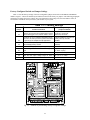
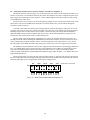
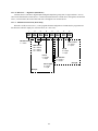
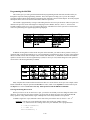
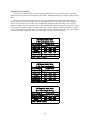
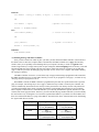
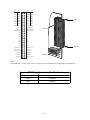
Factory-Configured Switch and Jumper Settings
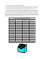
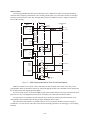
Table 1-1 lists the factory settings of the user-configurable jumpers and switch on the DM406 and DM5406
modules. Figure 1-1 shows the module layout and the locations of the factory-set jumpers. The following paragraphs
explain how to change the factory settings. Pay special attention to the setting of S1, the base address switch, to
avoid address contention when you first use your module in your system.
Table 1-1 — Factory Settings
Switch/
Jumper
Function Controlled
Factory Settings
(Jumpers Installed)
P3
Sets the clock sources for the 8254 timer/counters;
selects A/D trigger source; selects GATE 2 source
Jumpers installed on CLK0-OSC,
CLK2-OT1, PCLK-PCK,
TRIG-OT2, GT2-EG2
P4
Connects one of four software selectable interrupt
sources to an interrupt channel; pulls tri-state buffer
to ground (G) for multiple interrupt applications
Jumper installed on G (ground for
buffer); interrupt channels
disabled
P5
Sets the DMA request (DRQ) and DMA
acknowledge (DACK) channel
Disabled (DMA channel not
selected)
P6
Sets the analog input voltage range and polarity -5 to +5 volts
P7
Selects single-ended or differential analog input
type
P8
Sets the D/A output voltage range for DAC 1 ±5 (-5 to +5 volts)
P9
Sets the D/A output voltage range for DAC 2
S1
Sets
the
base
±5 (-5 to +5 volts)
address 300
hex
TR4
+
+
C31
BI
UNI
10V
20V
C32
Single-ended (jumpers installed
on three S pins)
DC1
+
C10
J5
+
C22
C11
10 +- 5
RN5
P7
S
S
D
S
D
R11
5
10 +-5
5
P8 DAC1
U5
U10
HI-508A
P9 DAC2
U6
C28
C5
C27
AD678
XTAL1
+
C13
D
C29
C16
C6
Y1
U9
+
C30
DC2
HI-508A
C34
C14
J7
P2
R4
R5
C15
C33
U8
PGA203
J4
P6 TR1
R3
C12
C20
J6
AD7237
EPLD
82C54
R12
C7 U3
C26
C23
PA
PCL
RN2
C4
SWITCH
82C55
C2
74HCT245
U1
V PCL G
RN1
C1
U2
PCH
PCH
32
P1B
P1A
+
P4
P5
P3
2
IRQ
5
3
6
4
7
G
3
1
DACK
1
3
OSC
OT1
XCK
OSC
XCK
TRIG
PCK
TRIG
OT2
EG2
5V
EG2
DRQ
C9
Made in USA
BASE ADDRESS
74HCT688
U4
S1
C8
+
U7
G
74HCT244
U11
R1
V
C3
Fig. 1-1 — Module Layout Showing Factory-Configured Settings
1-3
(768
P3 — 8254 Timer/Counter Sources (Factory Settings: See Table 1-1 & Figure 1-2)
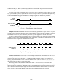
This header connector, shown in Figure 1-2, lets you select the clock sources for the 8254 timer/counters, TC0
and TC2. TC0 and TC1 are cascaded to form the pacer clock. This header is also used to configure the pacer clock
input, trigger input, and GATE 2 sources. Figure 1-3 shows a block diagram of the timer/counter circuitry to help
you in making these connections.
The clock source for TC0 and TC1 is selected by placing a jumper on OSC or XCK in the CLK0 section of the
header. OSC is the on-board 8-MHz clock and XCK is an external clock source you can connect through the
external I/O connector (P2-45).
To the left of the CLK0 pins are three pairs of pins grouped as CLK2 in the diagrams. These pins are used to
select the clock source for TC2. OT1 connects the output of TC1 (the pacer clock output) to the clock input of TC2.
Installing a jumper here cascades all three timer/counters, a feature necessary when using SIGNAL*MATH or
SIGNAL*VIEW software for data acquisition and control. OSC is the on-board 8 MHz clock, and XCK is connected to the same external clock source as CLK0-XCK (P2-45).
The next group of pins on this header, called PCLK, lets you use the on-board (internal) pacer clock or an
external pacer clock connected through the TRIGGER IN pin on the I/O connector (P2-39) to control A/D conversions. A jumper must be placed on PCK in order to use the internal pacer clock (output from TC1). Or, you can
place the jumper across TRIG and connect any external pacer clock source to P2-39 to trigger the A/D converter.
The TRIG pins select the hardware source used to trigger the burst mode when the external trigger enable bit at
BA + 5 is enabled. Bursts can be triggered from one of three hardware sources: TRIG, an external trigger signal
routed onto the board through P2-39; OT2, the output from timer/counter 2; or EG2, an external gate (EXT
GATE 2) signal routed onto the board through P2-46. When the trigger enable bit at BA + 5 is disabled, bursts are
triggered through software.
The last group of pins, GT2, select the gate source for timer/counter 2’s gate input. This jumper is provided so
that you can disconnect the GATE input for the third timer/counter from the EXT GATE 2 pin at the I/O connector
and tie the gate high if you are using the EXT GATE 2 pin as a trigger source.
GT2
TRIG
PCLK
CLK2
CLK0
(These labels not on board)
P3
OSC
XCK
OT1
OSC
XCK
PCK
TRIG
TRIG
OT2
EG2
EG2
+5V
Fig. 1-2 — 8254 Timer/Counter Sources Jumpers, P3
1-4
P3
8254
TIMER/
COUNTER
0
I/O CONNECTOR
P2
CLK0
8 MHz
CLOCK
CLK
+5 V
GATE
PIN 45
EXT CLK
PIN 41
EXT GATE 1
PIN 42
T/C OUT 1
PIN 44
T/C OUT 2
PIN 39
TRIGGER IN
PIN 46
EXT GATE 2
OUT
TIMER/
COUNTER
1
CLK
GATE
OUT
CLK2
TIMER/
COUNTER
2
8 MHz
CLOCK
CLK
GATE
OUT
PCLK
EPLD
PACER
CLOCK
INPUT
TRIG
TRIGGER
INPUT
GT2
+5 V
Fig. 1-3 — 8254 Timer/Counter Circuit Block Diagram
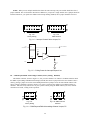
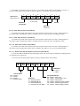
P4 — Interrupt Channel Select (Factory Setting: Jumper G; Interrupt Channel Disabled)
This header connector, shown in Figure 1-4, lets you connect any one of four software selectable interrupt
sources to an interrupt channel, IRQ2 (highest priority channel) through IRQ7 (lowest priority channel). To activate
a channel, you must install a jumper vertically across the desired IRQ channel. Figure 1-4a shows the factory
setting; Figure 1-4b shows the interrupt source connected to IRQ3.
This module supports an interrupt sharing mode where the pins labeled G connect a 1 kilohm pull-down
resistor to the output of a high-impedance tri-state driver which carries the interrupt request signal. This pull-down
resistor drives the interrupt request line low whenever interrupts are not active. Whenever an interrupt request is
made, the tri-state buffer is enabled, forcing the output high and generating an interrupt. You can monitor the
interrupt status through bit 2 in the status word (I/O address location BA + 0). After the interrupt has been
serviced, the reset command returns the IRQ line low, disabling the tri-state buffer, and pulling the output low
again. Figure 1-5 shows this circuit. Because the interrupt request line is driven low only by the pull-down
resistor, you can have two or more modules which share the same IRQ channel. You can tell which module issued
the interrupt request by monitoring each module’s IRQ status bit. If you are not planning on sharing interrupts or
if you are not sure that your CPU supports interrupt sharing, it is best to disable this feature and use the interrupts
in the normal mode. This will insure compatibility with all CPUs. See chapter 4 for details on disabling the
interrupt sharing circuit.
1-5
NOTE: When you use multiple modules that share the same interrupt, only one module should have the G
jumper installed. The rest should be disconnected. Whenever you operate a single module, the G jumper should be
installed. Whenever you operate the module with interrupt sharing disabled, the G jumper should be removed.
P4
P4
IRQ
IRQ
2
3
4
5
6
7
G
2
3
4
5
6
7
G
Fig. 1-4a:
Factory Setting
Fig. 1-4b:
IRQ3 Selected
Fig. 1-4 — Interrupt Channel Select Jumper, P4
I NT
SOURCE
I RQ STAT US
CLK
I NTERRUP T
R E GI S TE R
+5 V
I NT ERRUPT
CLR
CLR
P4
G
Fig. 1-5 — Pulling Down the Interrupt Request Line
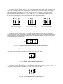
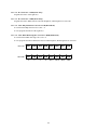
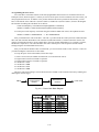
P5 — DMA Request/DMA Acknowledge Channel (Factory Setting: Disabled)
This header connector, shown in Figure 1-6, lets you select channel 1 or channel 3 for DMA transfers. Both
the DMA request (DRQ) and DMA acknowledge (DACK) lines must be jumpered for the same channel. This is
done by placing a jumper across the selected DRQ channel and a jumper across the same DACK channel. The
factory setting is disabled, as shown in Figure 1-6a. Figure 1-6b shows the module set for DMA transfers on
channel 1. Note that if any other device in your system is already using the DMA channel you select, channel
contention will result, causing erratic operation.
P5
P5
DACK
1
3
1
3
DRQ
DACK
1
3
1
3
DRQ
Fig. 1-6b: DMA Channel 1
Selected
Fig. 1-6a:
Factory Setting
Fig. 1-6 — DMA Request/DMA Acknowledge Channel Jumper, P5
1-6
P6 — Analog Input Voltage Range and Polarity (Factory Setting: ±5 volts)
This header connector, shown in Figure 1-7, lets you select the analog input voltage range and polarity. The
range is set by placing a jumper across the pair of pins labeled 20V, giving you a 20 volt range, or by placing a
jumper across the pair of pins labeled 10V, giving you a 10 volt range. The polarity is selected by placing a
jumper across the pins labeled UNI for 0 to +10 volts, or BI for ±5 or ±10 volts. Note that when you place a
jumper across 20V, you must place a second jumper across BI (±10 volts). The UNI polarity cannot be used with
the 20 volt input range. Figure 1-7 shows the three possible input voltage configurations.
BI
UNI
P6
Fig. 1-7b: -10 to +10 volts
Fig. 1-7a: -5 to +5 volts
(Factory Setting)
10V
20V
BI
UNI
10V
20V
BI
UNI
10V
20V
P6
P6
Fig. 1-7c: 0 to +10 volts
Fig. 1-7 — Analog Input Range and Polarity Jumper, P6
P7 — Single-Ended/Differential Analog Inputs (Factory Setting: Single-Ended)
This header connector, shown in Figure 1-8, configures the 406/5406 for 8 differential or 16 single-ended
analog input channels. When operating in the single-ended mode, three jumpers must be installed across the S pins.
When operating in the differential mode, the jumpers must be installed across the D pins. DO NOT install jumpers
across both S and D pins at the same time!
P7
S
D
S
D
S
D
Fig. 1-8 — Single-Ended/Differential Analog Input Signal Type Jumpers, P7
P8 — DAC 1 Output Voltage Range (Factory Setting: +5 to -5 volts)
This header connector, shown in Figure 1-9, sets the output voltage range for DAC 1 at 0 to +5, ±5, or 0 to +10
volts (right to left on the header). This header does not have to be set the same as P9.
P8 DAC1
10 ±5 5
Fig. 1-9 — DAC 1 Output Voltage Range Jumper, P8
P9 — DAC 2 Output Voltage Range (Factory Setting: +5 to -5 volts)
This header connector, shown in Figure 1-10, sets the output voltage range for DAC 2 at 0 to +5, ±5, or 0 to +10
volts (right to left on the header). This header does not have to be set the same as P8.
P9 DAC2
10 ±5 5
Fig. 1-10 — DAC 2 Output Voltage Range Jumper, P9
1-7
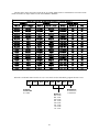
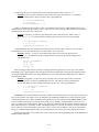
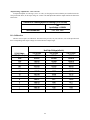
S1 — Base Address (Factory Setting: 300 hex (768 decimal))
One of the most common causes of failure when you are first trying your module is address contention. Some of
your computer’s I/O space is already occupied by internal I/O and other peripherals. When the module attempts to
use I/O address locations already used by another device, contention results and the board does not work.
To avoid this problem, the 406/5406 has an easily accessible DIP switch, S1, which lets you select any one of
32 starting addresses in the computer’s I/O. Should the factory setting of 300 hex (768 decimal) be unsuitable for
your system, you can select a different base address simply by setting the switches to any one of the values listed in
Table 1-2. The table shows the switch settings and their corresponding decimal and hexadecimal (in parentheses)
values. Make sure that you verify the order of the switch numbers on the switch (1 through 5) before setting them.
When the switches are pulled forward, they are OPEN, or set to logic 1, as labeled on the DIP switch package. When
you set the base address for your module, record the value in the table inside the back cover. Figure 1-11 shows the
DIP switch set for a base address of 300 hex (768 decimal).
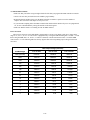
Table 1-2: Base Address Switch Settings, S1
Base Address
Decimal / (Hex)
Switch Setting
5 4 3 2 1
Base Address
Decimal / (Hex)
Switch Setting
5 4 3 2 1
512 / (200)
0 0 0 0 0
768 / (300)
1 0 0 0 0
528 / (210)
0 0 0 0 1
784 / (310)
1 0 0 0 1
544 / (220)
0 0 0 1 0
800 / (320)
1 0 0 1 0
560 / (230)
0 0 0 1 1
816 / (330)
1 0 0 1 1
576 / (240)
0 0 1 0 0
832 / (340)
1 0 1 0 0
592 / (250)
0 0 1 0 1
848 / (350)
1 0 1 0 1
608 / (260)
0 0 1 1 0
864 / (360)
1 0 1 1 0
624 / (270)
0 0 1 1 1
880 / (370)
1 0 1 1 1
640 / (280)
0 1 0 0 0
896 / (380)
1 1 0 0 0
656 / (290)
0 1 0 0 1
912 / (390)
1 1 0 0 1
672 / (2A0)
0 1 0 1 0
928 / (3A0)
1 1 0 1 0
688 / (2B0)
0 1 0 1 1
944 / (3B0)
1 1 0 1 1
704 / (2C0)
0 1 1 0 0
960 / (3C0)
1 1 1 0 0
720 / (2D0)
0 1 1 0 1
976 / (3D0)
1 1 1 0 1
736 / (2E0)
0 1 1 1 0
992 / (3E0)
1 1 1 1 0
752 / (2F0)
0 1 1 1 1
1008 / (3F0)
1 1 1 1 1
0 = closed, 1 = open
Fig. 1-11 — Base Address Switch, S1
1-8
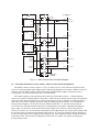
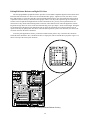
Pull-up/Pull-down Resistors on Digital I/O Lines
The 8255 programmable peripheral interface provides 16 TTL/CMOS compatible digital I/O lines which can be
interfaced with external devices. These lines are divided into three groups: eight Port A lines, four Port C Lower
lines, and four Port C Upper lines (Port B is used for internal board functions). You can install and connect pull-up
or pull-down resistors for any or all of these three groups of lines. You may want to pull lines up for connection to
switches. This will pull the line high when the switch is disconnected. Or, you may want to pull lines down for
connection to relays which control turning motors on and off. These motors turn on when the digital lines controlling them are high. The Port A lines of the 8255 automatically power up as inputs - which can float high - during the
few moments before the board is first initialized. This can cause the external devices connected to these lines to
operate erratically. By pulling these lines down, when the data acquisition system is first turned on, the motors will
not switch on before the 8255 is initialized.
To use the pull-up/pull-down feature, you must first install resistor packs in any or all of the three locations
around the 8255, labeled PA, PCL, and PCH. PA takes a 10-pin pack, and CL and CH take 6-pin packs. Figure 1-12
shows a blowup of the resistor pack locations.
V
G
PA
C23
C26
PCL
RN2
U1
V PCL G
C1
PCH
TR4
+
+
C31
BI
UNI
20V
10V
C32
DC1
+
C10
C20
J5
+
C22
C11
C13
U10
HI-508A
RN5
S
S
D
D
S
D
R11
10
+5
-
5
10
+5
-
5
P8 DAC1
P7
P9 DAC2
U6
U5
C28
C5
C27
AD678
+
XTAL1
C29
C16
C6
Y1
U9
+
C30
DC2
HI-508A
C34
C14
J7
P2
R4
R5
C15
C33
U8
PGA203
J4
P6 TR1
R3
C12
J6
AD7237
EPLD
82C54
R12
C7 U3
C26
C23
PA
PCL
RN2
C4
SWITCH
82C55
C2
74HCT245
U1
V PCL G
RN1
C1
U2
PCH
PCH
32
P1B
P1A
+
P4
P5
P3
2
IRQ
5
3
6
4
7
G
3
DACK
1
1
3
OT1
OSC
OSC
XCK
TRIG
XCK
TRIG
PCK
OT2
5V
EG2
EG2
DRQ
C9
Made in USA
BASE ADDRESS
74HCT688
U4
S1
C8
+
U7
G
74HCT244
U11
R1
V
C3
Fig. 1-12 — Pull-up/Pull-down Resistor Circuitry
1-9
PCH
After the resistor packs are installed, you must connect them into the circuit as pull-ups or pull-downs. Locate
the three-hole pads on the board near the resistor packs. They are labeled G (for ground) on one end and V (for Vcc)
on the other end. The middle hole is common. PA is for Port A, CL is for Port C Lower, and CH is for Port C Upper.
Figure 1-12 shows these pads. To operate as pull-ups, solder a jumper wire between the common pin (middle pin of
the three) and the V pin. For pull-downs, solder a jumper wire between the common pin (middle pin) and the G pin.
Figure 1-13 shows Port A lines with pull-ups, Port C Lower with pull-downs, and Port C Upper with no resistors.
+5 V
PA
8255
V
PULL- UP
G
10K
PORT A
(PA0-7)
+5 V
CL
PULL- DOWN
V
G
10K
PORT C
LOWER
( PC0- 3)
+5 V
CH
V
G
PORT C
UPPER
( PC4- 7)
Fig. 1-13 — Adding Pull-ups and Pull-downs to Digital I/O Lines
1-10
CHAPTER 2
INSTALLATION
The 406/5406 is easy to install in your cpuModule™ or other
PC/104 based system. This chapter tells you step-by-step how to
connect the module.
After you have made all of your connections, you can turn your
system on and run the 406DIAG board diagnostics program included on your example software disk to verify that your module is
working.
2-1
2-2
Installation
Keep the module in its antistatic bag until you are ready to install it in your cpuModule™ or other PC/104 based
system. When removing it from the bag, hold the module at the edges and do not touch the components or connectors.
Before installing the module in your system, check the jumper and switch settings. Chapter 1 reviews the
factory settings and how to change them. If you need to change any settings, refer to the appropriate instructions in
Chapter 1. Note that incompatible jumper settings can result in unpredictable module operation and erratic response.
The DM406 and DM5406 come with a stackthrough P1 connector. The stackthrough connector lets you stack
another module on top of your module, plugging it into the data bus through the pins on the non-component side of
the module.
To install the module , follow the procedures described in the computer manual and the steps below:
1. Turn OFF the power to your system.
2. Touch a metal rack to discharge any static buildup and then remove the board from its antistatic bag.
3. Select the appropriate standoffs for your application to secure the module when you install it in your system
(two sizes are included with the module).
4. Holding the module by its edges, orient it so that the P1 bus connector’s pin 1 lines up with pin 1 of the
expansion connector onto which you are installing the module.
5. After carefully positioning the module so that the card edge connector is resting on the expansion connector,
gently and evenly press down on the module until it is secured on the connector.
NOTE: Do not force the module onto the connector. If the module does not slide into place, remove it and
try again. Wiggling the module or exerting too much pressure can result in damage to the 406/5406 or to the
computer module.
6. After the module is installed, connect the cable to I/O connector P2 on the module. When making this
connection, note that there is no keying to guide you in orientation. You must make sure that pin 1 of the
cable is connected to pin 1 of P2 (pin 1 is marked on the board with a small square). For twisted pair cables,
pin 1 is the dark brown wire; for standard single wire cables, pin 1 is the red wire.
7. Make sure all connections are secure.
External I/O Connections
Figure 2-1 shows the 406/5406’s P2 I/O connector pinout. Refer to this diagram as you make your I/O connections. Note that +12 volts at pin 47 and -12 volts at pin 49 are available only if your computer bus supplies them
(these voltages are not provided by the board).
2-3
DIFF.
S.E.
DIFF.
S.E.
AIN1+
AIN1
1
2
AIN1-
AIN9
AIN2+
AIN2
3
4
AIN2-
AIN10
AIN3+
AIN3
5
6
AIN3-
AIN11
AIN4+
AIN4
7
8
AIN4-
AIN12
AIN5+
AIN5
9
10
AIN5-
AIN13
AIN6+
AIN6
11 12
AIN6-
AIN14
AIN7+
AIN7
13 14
AIN7-
AIN15
AIN8+
AIN8
15 16
AIN8-
AIN16
AOUT 1
17 18
ANALOG GND
AOUT 2
19 20
ANALOG GND
ANALOG GND
21 22
ANALOG GND
PA7
23 24
PC7
PA6
25 26
PC6
PA5
27 28
PC5
PA4
29 30
PC4
PA3
31 32
PC3
PA2
33 34
PC2
PA1
35 36
PC1
PA0
37 38
PC0
TRIGGER IN
39 40
DIGITAL GND
EXT GATE 1
41 42
T/C OUT 1
TRIGGER OUT
43 44
T/C OUT 2
EXT CLK
45 46
EXT GATE 2
+12 VOLTS
47 48
+5 VOLTS
-12 VOLTS
49 50
DIGITAL GND
Fig. 2-1 — P2 I/O Connector Pin Assignments
Connecting the Analog Input Pins
The analog inputs on the module can be set for single-ended or differential operation.
NOTE: It is good practice to connect all unused channels to ground, as shown in the following diagrams.
Failure to do so may affect the accuracy of your results.
Single-Ended. When operating in the single-ended mode, connect the high side of the analog input to one of
the analog input channels, AIN1 through AIN16, and connect the low side to an ANALOG GND (pins 18 and 20-22
on P2). Figure 2-2 shows how these connections are made.
Differential. When operating in the differential mode, twisted pair cable is recommended to reduce the effects
of magnetic coupling at the inputs. Your signal source may or may not have a separate ground reference. When
using the differential mode, you should install a 10 kilohm resistor pack at location RN5 on the module to provide a
reference to ground for signal sources without a separate ground reference.
First, connect the high side of the analog input to the selected analog input channel, AIN1+ through AIN8+, and
connect the low side of the input to the corresponding AIN- pin. Then, for signal sources with a separate ground
reference, connect the ground from the signal source to an ANALOG GND (pins 18 and 20-22 on P2). Figure 2-3
shows how these connections are made.
2-4
I / O C O N N E C TO R
P2
SIGNAL
SOURCE
1 OUT
+
PIN 1
AIN 1
GND
MUX
SIGNAL
SOURCE
7 OUT
+
P I N 14
OUT +
+
OUT -
-
A I N 15
GND
P I N 16
A I N 16
P I N 22
Fig. 2-2 — Single-Ended Input Connections
I / O C O N N E C TO R
P2
SIGNAL
+
SOURCE
1 OUT
PI N 1
-
PI N 2
AI N 1+
RN5
AI N 110K
MUX
SIGNAL
+
SOURCE
7 OUT
PI N 13
-
PI N 14
OUT +
+
OUT -
-
AI N 7+
AI N 710K
GND
PI N 15
AI N 8+
PI N 16
10K
AI N 8-
PI N 22
Fig. 2-3 — Differential Input Connections
2-5
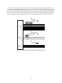
Connecting the Trigger In and Trigger Out Pins, Cascading Modules
The 406/5406 has an external trigger input (P2-39) and output (P2-43) so that conversions can be started based
on external events, or so that two or more modules can be cascaded and run synchronously in a “master/slave”
configuration. By cascading two (or more) modules as shown in Figure 2-4, they can be triggered to start an A/D
conversion at the same time (sampling uncertainty is less than 50 nanoseconds). When you cascade modules, be sure
to set each module for a different base address (see Chapter 1), or system contention will result.
NOTE: When cascading modules, the sampling uncertainty is less than 50 nanoseconds. If this level of
uncertainty is too great for your application, you can connect the trigger signal to the trigger input of each board. In
this configuration, the modules are not cascaded, but rather driven by the same trigger pulse at the same time, and
the sampling uncertainty is reduced to less than 5 nanoseconds.
If you apply an external trigger to the board’s trigger in pin, note that a jumper should be installed on
PCLK-TRIG on P3 (see Chapter 1). The module is triggered on the positive edge of the pulse and the pulse duration
should be at least 100 nanoseconds.
I / O C O N N E C TO R
P2
BOARD #1
(MASTER)
MUX
SIGNAL
SOURCE
1 OUT
+
-
PI N 1
CH 1
PI N 2
CH 1
AI N1 +
AI N1 -
10K
PI N 43
T RI GGER OUT
BOARD #2
( S LAV E )
MUX
SIGNAL
SOURCE
2 OUT
+
-
PI N 1
CH 1
PI N 2
CH 1
10K
AI N1 +
AI N1 -
PI N 39
T RI GGER I N
Fig. 2-4 — Cascading Two Modules for Simultaneous Sampling
Connecting the Analog Outputs
For each of the two D/A outputs, connect the high side of the device receiving the output to the AOUT channel
(P2-17 or P2-19) and connect the low side of the device to an ANALOG GND (P2-18 or P2-20).
Connecting the Timer/Counters and Digital I/O
For all of these connections, the high side of an external signal source or destination device is connected to the
appropriate signal pin on the I/O connector, and the low side is connected to any DIGITAL GND.
Running the 406DIAG Diagnostics Program
Now that your module is ready to use, you will want to try it out. An easy-to-use, menu-driven diagnostics
program, 406DIAG, is included with your example software to help you verify your module’s operation. You can
also use this program to make sure that your current base address setting does not contend with another device.
2-6
CHAPTER 3
HARDWARE DESCRIPTION
This chapter describes the features of the DM406 and DM5406
hardware. The major circuits are the A/D, the D/A, the timer/
counters, and the digital I/O lines.
3-1
3-2
The406/5406 has four major circuits, the A/D, the D/A, the timer/counters, and the digital I/O lines. Figure 3-1
shows the block diagram of the module. This chapter describes the hardware which makes up the major circuits.
DATA
DMA
CONTROL
AND
SELECT
12-BIT
A/D
CONVERTER
RANGE
SELECT
±5 VOLTS
0 TO +10 VOLTS
±10 VOLTS
PROGRAMMABLE
GAIN
AMPLIFIER
1/2/4/8
MUX
16 ANALOG INPUTS
8 DIFF./16 S.E.
-5V TO +5V
0 TO +10V
-10V TO +10V
16
TRIGGER IN
TRIGGER
SELECT
TRIGGER OUT
CHANNEL
SCAN/BURST
CIRCUITRY
8255
PPI
8
PORT B
8
PORT A
8
PORT C
PULL-UP/DOWN
RESISTORS
PC BUS
8 MHz
OSC
TIMER/
COUNTER
I/O AND
PACER CLOCK
SELECT
8254
PIT
ADDRESS
I/O CONNECTOR
INTERRUPT
SELECT
5
ADDRESS
DECODE
CONTROL
RANGE
SELECT
±5 VOLTS
0 TO +5 VOLTS
0 TO +10 VOLTS
12-BIT
D/A
CONVERTER
AOUT 1
AOUT 2
+5 VOLTS
±12 VOLTS
DC/DC
CONVERTER
±15 VOLTS
±12 VOLTS
DM5406 ONLY
CONTROL
+5 VOLTS
Fig. 3-1 — 406/5406 Block Diagram
A/D Conversion Circuitry
The DM406 and DM5406 perform analog-to-digital conversions on up to 8 differential or 16 single-ended
software-selectable analog input channels. The following paragraphs describe the A/D circuitry.
Analog Inputs
The input voltage range is jumper-selectable for -5 to +5 volts, -10 to +10 volts, or 0 to +10 volts. Softwareprogrammable binary gains of 1, 2, 4, and 8 let you amplify lower level signals to more closely match the module’s
input ranges. Overvoltage protection to ±35 volts is provided at the inputs.
A/D Converter
The AD678 12-bit successive approximation A/D converter accurately digitizes dynamic input voltages in
5 microseconds, for a maximum throughput rate of 200 kHz for the converter alone. The AD678 contains a sampleand-hold amplifier, a 12-bit A/D converter, a 5-volt reference, a clock, and a digital interface to provide a complete
A/D conversion function on a single chip. Its low-power CMOS logic combined with a high-precision, low-noise
design give you accurate results.
Conversions are initiated through software (internally triggered) or by an external trigger brought onto the board
through the I/O connector. An on-board or external pacer clock can be used to control the conversion rate. Conversion modes are described in Chapter 4, Module Operation and Programming.
3-3
Data Transfer
The converted data can be transferred through the PC data bus to PC memory in one of two ways: by using the
microprocessor or by using direct memory access (DMA). Data bus transfers take more processor time to execute.
They use polling and interrupts to determine when data has been acquired and is ready for transfer. DMA places
data directly into the PC’s memory, one byte at a time, with minimal use of processor time. DMA transfers are
managed by the DMA controller as a background function of the PC, letting you operate at higher throughput rates.
The maximum throughput rate of the module is 100 kHz.
D/A Converters (-2 Module)
Two independent 12-bit analog output channels are included on the DM406-2 and DM5406-2. The analog
outputs are generated by two 12-bit D/A converters with independent jumper-selectable output ranges of ±5, 0 to +5,
or 0 to +10 volts. The 10-volt ranges have a resolution of 2.44 millivolts, and the 5-volt range has a resolution of
1.22 millivolts.
Timer/Counters
An 8254 programmable interval timer provides three 16-bit, 8-MHz timer/counters to support a wide range of
timing and counting functions. Two of the timer/counters, TC0 and TC1, are cascaded so that they can be used for
the pacer clock. The pacer clock is described in Chapter 4. You can use the remaining timer/counter, TC2, for
counting applications, or cascade it to TC0 and TC1 for timing applications. Figure 3-2 shows the timer/counter
circuitry.
P3
8254
TIMER/
COUNTER
0
I/O CONNECTOR
P2
CLK0
8 MHz
CLOCK
CLK
+5 V
GATE
PIN 45
EXT CLK
PIN 41
EXT GATE 1
PIN 42
T/C OUT 1
PIN 44
T/C OUT 2
PIN 39
TRIGGER IN
PIN 46
EXT GATE 2
OUT
TIMER/
COUNTER
1
CLK
GATE
OUT
CLK2
TIMER/
COUNTER
2
8 MHz
CLOCK
CLK
GATE
OUT
PCLK
EPLD
PACER
CLOCK
INPUT
TRIG
TRIGGER
INPUT
GT2
+5 V
Fig. 3-2 — 8254 Timer/Counter Circuit Block Diagram
3-4
Each timer/counter has two inputs, CLK in and GATE in, and one output, timer/counter OUT. They can be
programmed as binary or BCD down counters by writing the appropriate data to the command word, as described in
Chapter 4. The command word also lets you set up the mode of operation. The six programmable modes are:
Mode 0
Mode 1
Mode 2
Mode 3
Mode 4
Mode 5
Event Counter (Interrupt on Terminal Count)
Hardware-Retriggerable One-Shot
Rate Generator
Square Wave Mode
Software-Triggered Strobe
Hardware Triggered Strobe (Retriggerable)
These modes are detailed in the 8254 Data Sheet, reprinted from Intel in Appendix C.
Digital I/O, Programmable Peripheral Interface
The programmable peripheral interface (PPI) is used for digital I/O functions. This high-performance TTL/
CMOS compatible chip has 24 digital I/O lines divided into two groups of 12 lines each:
Group A — Port A (8 lines) and Port C Upper (4 lines);
Group B — Port B (8 lines) and Port C Lower (4 lines).
The eight lines in Port B are used for on-board functions. The 16 remaining lines, Port A, Port C Lower, and
Port C Upper, are available for your use. You can use these ports in one of these three PPI operating modes:
Mode 0 — Basic input/output. Lets you use simple input and output operation for a port. Data is written to or
read from the specified port.
Mode 1 — Strobed input/output. Lets you transfer I/O data from Port A in conjunction with strobes or handshaking signals.
Mode 2 — Strobed bidirectional input/output. Lets you communicate bidirectionally with an external device
through Port A. Handshaking is similar to Mode 1.
These modes are detailed in the 8255 Data Sheet, reprinted from Intel in Appendix C.
3-5
3-6
CHAPTER 4
MODULE OPERATION AND PROGRAMMING
This chapter shows you how to program and use your 406/
5406. It provides a complete description of the I/O map, a detailed
description of programming operations and operating modes, and
flow diagrams to aid you in programming. The example programs
included on the disk in your module package are listed at the end
of this chapter. These programs, written in Turbo C, Turbo Pascal,
and BASIC, include source code to simplify your applications
programming.
4-1
4-2
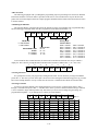
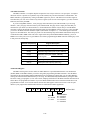
Defining the I/O Map
The I/O map for the 406/5406 is shown in Table 4-1 below. As shown, the module occupies 16 consecutive I/O
port locations. The base address (designated as BA) can be selected using DIP switch S1 as described in Chapter 1,
Module Settings. This switch can be accessed without removing the board from the connector. S1 is factory set at
300 hex (768 decimal). The following sections describe the register contents of each address used in the I/O map.
Table 4-1 DM406/DM5406 I/O Map
Register Description
Read Function
Write Function
Address *
(Decimal)
Read Status/Start Convert Read status word
Start A/D conversion
Read converted data, MSB first, Simultaneously update DAC 1 and
DAC 2 (-2 version)
Read Data/Update DACs then LSB
Reset board so that it is ready to
start A/D conversions
Reset
Reserved
Program number of scan/burst
channels; enable scan/burst;
select IRQ source
Scan/Burst
Read current settings
BA + 0
8255 PPI Port A
8255 PPI Port B
(Channel/Gain/ Board
Functions)
Read Port A digital input lines
Program Port A digital output lines
BA + 4
Read channel & gain; external
trigger enable, IRQ enable
Program channel & gain; external
trigger enable, IRQ enable
BA + 5
8255 PPI Port C
Read Port C digital input lines
Program Port C digital output lines
BA + 6
8255 PPI Control Word
Reserved
Program PPI configuration
BA + 7
Load count register
BA + 8
Load count register
BA + 9
Load count register
BA + 10
Program counter mode
BA + 11
8254 Timer/Counter 0
(Used for pacer clock)
Read count value
8254 Timer/Counter 1
(Used for pacer clock)
Read count value
8254 Timer/Counter 2
(Available for external use)Read count value
8254 Timer/Counter Control
Word
Disable Interrupt Sharing
BA + 1
BA + 2
BA + 3
D/A Converter 1 LSB
Reserved
Program DAC1 LSB (-2 version)
BA + 12
D/A Converter 1 MSB
Clear IRQ/
D/A Converter 2 LSB
Clear DMA Done/
D/A Converter 2 MSB
Reserved
Program DAC1 MSB (-2 version)
BA + 13
Clear IRQ status
Program DAC2 LSB (-2 version)
BA + 14
Clear DMA done flag
Program DAC2 MSB (-2 version)
BA + 15
* BA = Base Address
4-3
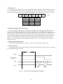
BA + 0: Read Status/Start Convert (Read/Write)
A read provides the six status bits defined below. The end-of-convert bit goes high when a conversion is
complete and does not go low until the data is read, useful information when using external triggering to start
conversions. The DMA done bit goes high when you are in the DMA mode and the DMA transfer is complete. The
IRQ status bit goes high when an interrupt has occurred and stays high until a clear IRQ command is sent (BA + 14).
D3 shows the status of the burst trigger source jumpered at P3-TRIG. D5 shows whether interrupt sharing is
enabled or disabled. D6 shows the status of the PCLK line jumpered at P3. Unlike the EOC status at bit 0, the A/D
converter status, D7, goes low when a conversion starts and then goes high as soon as the conversion is completed. When the input has been sampled and a conversion is in progress, this line goes low. At this time, the
analog input channel can be changed, allowing maximum throughput for scanning channels through software.
A write starts an A/D conversion (data written is irrelevant).
D7 D6 D5 D4 D3 D2 D1 D0
X
End-of-Convert
0 = no EOC
1 = conversion done
A/D CONVERTER Status
0 = converting
1 = not converting
P3-TRIG Status
monitors the TRIG
line selected on P3
P3-PCLK Status
monitors the PCLK line
selected on P3
IRQ Sharing Status
0 = Enabled
1 = Disabled
DMA Done
0 = DMA not done
1 = DMA done
IRQ Status
0 = No IRQ
1 = IRQ
BA + 1: Read A/D Data/Update DAC Outputs (Read/Write)
Two successive reads provide the MSB first, followed by the LSB, for each A/D conversion, as defined
below. If a conversion is started before this data is read from the previous conversion, the data will be lost. A
write simultaneously starts a D/A conversion in both DACs (data written is irrelevant). If the data has not been
updated since the last conversion, the output of the DAC will not change.
MSB
D7 D6 D5 D4 D3 D2 D1 D0
x
LSB
x
x
x
Bit 11
Bit 10
Bit 9
Bit 8
D7 D6 D5 D4 D3 D2 D1 D0
Bit 7
Bit 6
Bit 5
Bit 4
Bit 3
Bit 2
Bit 1
Bit 0
BA + 2: Reset (Write Only)
Resets certain bits or registers so that the board is ready to start conversions. The data written is irrelevant; the
act of writing to this address clears the board. A reset command sets the internal byte pointer to read the MSB on the
next read, resets the DRQ and IRQ registers, clears the EPLD scan/burst circuitry, and clears the DMA done bit,
BA + 0, bit 1.
4-4
BA + 3: Scan/Burst (Read/Write)
Bits D0 through D3 program the number of consecutive analog input channels to be scanned or bursted. The
channel scan or burst begins with the channel selected at BA + 5.
Bits D4 and D5 program one of four IRQ sources available for generating interrupts. The IRQ channel is set by
the jumper on P4. The IRQ is enabled at bit 7, BA + 5.
Bits D6 and D7 enable the scan or burst mode. Each time you start a new scan or burst, you should first reset
the board by writing to BA + 2 or by programming these bits to disable scan/burst, and then follow that step by
enabling the scan or burst mode. This ensures that the EPLD scan/burst counter circuitry is cleared.
A read tells you the bit settings.
D7 D6 D5 D4 D3 D2 D1 D0
Scan/Burst Enable
00 = disabled
01 = reserved
10 = scan enabled
11 = burst enabled
IRQ Source Select
00 = A/D start convert
01 = DMA done
10 = trigger (P3-TRIG)
11 = pacer clock (P3-PCLK)
Number of
Channels Scanned
0000 = 1 channel
0001 = 2 channels
0010 = 3 channels
0011 = 4 channels
0100 = 5 channels
0101 = 6 channels
0110 = 7 channels
0111 = 8 channels
1000 = 9 channels
1001 = 10 channels
1010 = 11 channels
1011 = 12 channels
1100 = 13 channels
1101 = 14 channels
1110 = 15 channels
1111 = 16 channels
BA + 4: PPI Port A — Digital I/O (Read/Write)
Transfers the 8-bit Port A digital input and digital output data between the board and an external device. A read
transfers data from the external device, through P2, and into PPI Port A; a write transfers the written data from Port
A through P2 to an external device.
BA + 5: PPI Port B — Channel/Gain/Board Functions Select (Read/Write)
A write programs the analog input channel and gain, and enables the IRQ and external trigger. Note that,
because some of the Port B bits are built into the EPLD, writing to the 8255 control word does not automatically set
the Port B bits to zero as it does in a typical 8255 configuration. Therefore, you must write a zero to Port B to ensure
all bits are zero whenever you desire to reset this port.
Reading this register shows you the current settings.
D7 D6 D5 D4 D3 D2 D1 D0
IRQ Enable
0 = IRQ disabled
1 = IRQ enabled
EXT PCK/EXT TRIG
Enable
0 = Disabled
1 = Enabled
Analog Input
Channel Select
0000 = channel 1
0001 = channel 2
0010 = channel 3
0011 = channel 4
0100 = channel 5
0101 = channel 6
0110 = channel 7
0111 = channel 8
Channel Gain
00 = x1
01 = x2
10 = x4
11 = x8
4-5
1000 = channel 9
1001 = channel 10
1010 = channel 11
1011 = channel 12
1100 = channel 13
1101 = channel 14
1110 = channel 15
1111 = channel 16
BA + 6: PPI Port C — Digital I/O (Read/Write)
Transfers the two 4-bit Port C digital input and digital output data groups (Port C Upper and Port C Lower)
between the board and an external device. A read transfers data from the external device, through P2, and into PPI
Port C; a write transfers the written data from Port C through P2 to an external device.
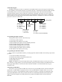
BA + 7: 8255 PPI Control Word (Write Only)
When bit 7 of this word is set to 1, a write programs the PPI configuration. The PPI must be programmed so
that Port B is a Mode 0 output port, as shown below (X = don’t care).
1
X
X
X
X
0
0
X
D7 D6 D5 D4 D3 D2 D1 D0
Mode Set Flag
1 = active
Port C Lower
0 = output
1 = input
Mode Select
00 = mode 0
01 = mode 1
10 = mode 2
Port B
0 = output
1 = input
Port A
0 = output
1 = input
Port C Upper
0 = output
1 = input
Group A
4-6
Mode Select
0 = mode 0
1 = mode 1
Group B
The table below shows the control words for the 16 possible Mode 0 Port I/O combinations. The control words
which set Port B as an input cannot be used on the DM406 or DM5406.
8255 Por t I/O Flow Dir ection and Contr ol Wor ds , Mode 0
Gr oup A
Gr oup B
Contr ol Wor d
Por t A
Por t C Upper
Por t B
Por t C Low er
Binar y
Decim al
Hex
Output
Output
Output
Output
10000000
128
80
Output
Output
Output
Input
10000001
129
81
Output
Output
Input
Output
10000010
130
82
Output
Output
Input
Input
10000011
131
83
Output
Input
Output
Output
10001000
136
88
Output
Input
Output
Input
10001001
137
89
Output
Input
Input
Output
10001010
138
8A
Output
Input
Input
Input
10001011
139
8B
Input
Output
Output
Output
10010000
144
90
Input
Output
Output
Input
10010001
145
91
Input
Output
Input
Output
10010010
146
92
Input
Output
Input
Input
10010011
147
93
Input
Input
Output
Output
10011000
152
98
Input
Input
Output
Input
10011001
153
99
Input
Input
Input
Output
10011010
154
9A
Input
Input
Input
Input
10011011
155
9B
When bit 7 of the PPI control word is set to 0, a write can be used to individually program the Port C lines.
D7 D6 D5 D4 D3 D2 D1 D0
Set/Reset
Function Bit
0 = active
Bit Select
000 = PC0
001 = PC1
010 = PC2
011 = PC3
100 = PC4
101 = PC5
110 = PC6
111 = PC7
4-7
Bit Set/Reset
0 = set bit to 0
1 = set bit to 1
For example, if you want to set Port C bit 0 to 1, you would set up the control word so that bit 7 is 0; bits 1, 2,
and 3 are 0 (this selects PC0); and bit 0 is 1 (this sets PC0 to 1). The control word is set up like this:
0
Sets PC0 to 1:
(written to BA +7)
X
X
X
0
0
0
1
D7 D6 D5 D4 D3 D2 D1 D0
X = don’t care
Set PC0
Set/Reset
Function Bit
Bit Select
000 = PC0
BA + 8: 8254 Timer/Counter 0 (Read/Write)
A read shows the count in the counter, and a write loads the counter with a new value. Counting begins as
soon as the count is loaded. This counter is cascaded with TC1 to form the 32-bit on-board pacer clock.
BA + 9: 8254 Timer/Counter 1 (Read/Write)
A read shows the count in the counter, and a write loads the counter with a new value. Counting begins as
soon as the count is loaded. This counter is cascaded with TC0 to form the 32-bit on-board pacer clock.
BA + 10: 8254 Timer/Counter 2 (Read/Write)
A read shows the count in the counter, and a write loads the counter with a new value. Counting begins as
soon as the count is loaded. This counter can be cascaded to TC0 and TC1 or it can be used independently.
BA + 11: Disable Interrupt Sharing/8254 Control Word (Read/Write)
A read at this address disables the interrupt sharing circuit. The circuit can be re-enabled by resetting the CPU
or cycling the power off and on.
A write accesses the 8254 control register to directly control the three timer/counters.
D7 D6 D5 D4 D3 D2 D1 D0
BCD/Binary
0 = binary
1 = BCD
Counter Select
00 = Counter 0
01 = Counter 1
10 = Counter 2
11 = read back setting
Read/Load
00 = latching operation
01 = read/load LSB only
10 = read/load MSB only
11 = read/load LSB, then MSB
4-8
Counter Mode Select
000 = Mode 0, event count
001 = Mode 1, programmable 1-shot
010 = Mode 2, rate generator
011 = Mode 3, square wave rate generator
100 = Mode 4, software-triggered strobe
101 = Mode 5, hardware-triggered strobe
BA + 12: D/A Converter 1 LSB (Write Only)
Programs the DAC1 LSB (eight bits).
BA + 13: D/A Converter 1 MSB (Write Only)
Programs the DAC1 MSB (four bits) into D0 through D3; D4 through D7 are irrelevant.
BA + 14: Clear IRQ Status/D/A Converter 2 LSB (Read/Write)
A read clears the IRQ status bit at bit 2, BA + 0.
A write programs the DAC2 LSB (eight bits).
BA + 15: Clear DMA Done Flag/D/A Converter 2 MSB (Read/Write)
A read clears the DMA done flag at bit 1, BA + 0.
A write programs the DAC2 MSB (four bits) into D0 through D3; D4 through D7 are irrelevant.
DAC LSB
D7 D6 D5 D4 D3 D2 D1 D0
Bit 7
DAC MSB
Bit 6
Bit 5
Bit 4
Bit 3
Bit 2
Bit 1
Bit 0
D7 D6 D5 D4 D3 D2 D1 D0
X
X
X
X
Bit 11
4-9
Bit 10
Bit 9
Bit 8
Programming the 406/5406
This section gives you some general information about programming and the 406/5406, and then walks you
through the major 406/5406 programming functions. These descriptions will help you as you use the example
programs included with the board and the programming flow diagrams at the end of this chapter. All of the program
descriptions in this section use decimal values unless otherwise specified.
The module is programmed by writing to and reading from the correct I/O port locations. These I/O ports were
defined in the previous section. Most high-level languages such as BASIC, Pascal, C, and C++, and of course
assembly language, make it very easy to read/write these ports. The table below shows you how to read from and
write to I/O ports using some popular programming languages.
Language
BASIC
Turbo C
Turbo Pascal
Assembly
Read
Data=INP(Address)
Data=inportb(Address)
Data:=Port[Address]
mov dx , Address
in al, dx
Write
OUT Address, Data
outportb(Address, Data)
Port[Address]:=Data
mov dx , Address
mov al, Data
out dx , al
In addition to being able to read/write the I/O ports on the 406/5406, you must be able to perform a variety of
operations that you might not normally use in your programming. The table below shows you some of the operators
discussed in this section, with an example of how each is used with Pascal, C, and BASIC. Note that the modulus
operator is used to retrieve the least significant byte (LSB) of a two-byte word, and the integer division operator is
used to retrieve the most significant byte (MSB).
Language
C
Pascal
BASIC
Modules Integer Division
AND
OR
%
/
&
I
a=b% c
a = b/c
a = b&c
a = bIc
MOD
DIV
AND
OR
a :=b MOD c
a:=b DIV c
a := b AND c a :=b OR c
MOD
\ (back slash)
AND
OR
a = b MOD c
a = b\c
a = b AND c a = b OR c
Many compilers have functions that can read/write either 8 or 16 bits from/to an I/O port. For example, Turbo
Pascal uses Port for 8-bit port operations and PortW for 16 bits, Turbo C uses inportb for an 8-bit read of a port
and inport for a 16-bit read. Be sure to use only 8-bit operations with the DM406 or DM5406!
Clearing and Setting Bits in a Port
When you clear or set one or more bits in a port, you must be careful that you do not change the status of the
other bits. You can preserve the status of all bits you do not wish to change by proper use of the AND and OR
binary operators. Using AND and OR, single or multiple bits can be easily cleared in one operation.
To clear a single bit in a port, AND the current value of the port with the value b, where b = 255 - 2 bit.
Example: Clear bit 5 in a port. Read in the current value of the port, AND it with 223
(223 = 255 - 25), and then write the resulting value to the port. In BASIC, this is programmed as:
V = INP(PortAddress)
V = V AND 223
OUT PortAddress, V
4-10
To set a single bit in a port, OR the current value of the port with the value b, where b = 2bit.
Example: Set bit 3 in a port. Read in the current value of the port, OR it with 8 (8 = 23), and then
write the resulting value to the port. In Pascal, this is programmed as:
V := Port[PortAddress];
V := V OR 8;
Port[PortAddress] := V;
Setting or clearing more than one bit at a time is accomplished just as easily. To clear multiple bits in a port,
AND the current value of the port with the value b, where b = 255 - (the sum of the values of the bits to be cleared).
Note that the bits do not have to be consecutive.
Example: Clear bits 2, 4, and 6 in a port. Read in the current value of the port, AND it with 171
(171 = 255 - 22 - 24 - 26), and then write the resulting value to the port. In C, this is programmed
as:
v = inportb(port_address);
v = v & 171;
outportb(port_address, v);
To set multiple bits in a port, OR the current value of the port with the value b, where b = the sum of the
individual bits to be set. Note that the bits to be set do not have to be consecutive.
Example: Set bits 3, 5, and 7 in a port. Read in the current value of the port, OR it with 168
(168 = 23 + 25 + 27), and then write the resulting value back to the port. In assembly language, this
is programmed as:
mov dx, PortAddress
in al, dx
or al, 168
out dx, al
Often, assigning a range of bits is a mixture of setting and clearing operations. You can set or clear each bit
individually or use a faster method of first clearing all the bits in the range then setting only those bits that must be
set using the method shown above for setting multiple bits in a port. The following example shows how this twostep operation is done.
Example: Assign bits 3, 4, and 5 in a port to 101 (bits 3 and 5 set, bit 4 cleared). First, read in the
port and clear bits 3, 4, and 5 by ANDing them with 199. Then set bits 3 and 5 by ORing them
with 40, and finally write the resulting value back to the port. In C, this is programmed as:
v = inportb(port_address);
v = v & 199;
v = v | 40;
outportb(port_address, v);
A final note: Don’t be intimidated by the binary operators AND and OR and try to use operators for which you
have a better intuition. For instance, if you are tempted to use addition and subtraction to set and clear bits in place
of the methods shown above, DON’T! Addition and subtraction may seem logical, but they will not work if you try
to clear a bit that is already clear or set a bit that is already set. For example, you might think that to set bit 5 of a
port, you simply need to read in the port, add 32 (25) to that value, and then write the resulting value back to the port.
This works fine if bit 5 is not already set. But, what happens when bit 5 is already set? Bits 0 to 4 will be unaffected
and we can’t say for sure what happens to bits 6 and 7, but we can say for sure that bit 5 ends up cleared instead of
being set. A similar problem happens when you use subtraction to clear a bit in place of the method shown above.
Now that you know how to clear and set bits, we are ready to look at the programming steps for the DM406 and
DM5406 module functions.
4-11
A/D Conversions
The following paragraphs walk you through the programming steps for performing A/D conversions. Detailed
information about the conversion modes is presented in this section. You can follow these steps on the flow diagrams at the end of this chapter and in our example programs included with the board. In this discussion, BA refers
to the base address.
• Initializing the 8255 PPI
The eight Port B lines of the 8255 PPI control the channel selection, programmable gain, programmable IRQ,
and external trigger and DMA enable. Port B is programmed at I/O address location BA + 5:
D7 D6 D5 D4 D3 D2 D1 D0
IRQ Enable
0 = IRQ disabled
1 = IRQ enabled
EXT PCK/EXT TRIG
Enable
0 = Disabled
1 = Enabled
Analog Input
Channel Select
0000 = channel 1
0001 = channel 2
0010 = channel 3
0011 = channel 4
0100 = channel 5
0101 = channel 6
0110 = channel 7
0111 = channel 8
Channel Gain
00 = x1
01 = x2
10 = x4
11 = x8
1000 = channel 9
1001 = channel 10
1010 = channel 11
1011 = channel 12
1100 = channel 13
1101 = channel 14
1110 = channel 15
1111 = channel 16
To use Port B for these control functions, the 8255 must be initialized so that Port B is set up as a Mode 0
output port. This is done by writing this data to the PPI control word at I/O address BA + 7 (X = don’t care):
1
X
X
X
X
0
0
X
D7 D6 D5 D4 D3 D2 D1 D0
• Clearing the Board
It is good practice to start your program by resetting the 406/5406. You can do this by writing to the RESET
port at BA + 2. The value you write to this port is irrelevant. After resetting the board following power-up, you must
take an A/D reading and throw it away to make sure the converter is initialized and contains no unwanted data.
• Selecting a Channel
To select a conversion channel or the starting channel for a scan or burst, you must assign values to bits 0
through 3 in the PPI Port B port at BA + 5. The table below shows you how to determine the bit settings. Channels
9-16 are available in single-ended operation only. Note that if you do not want to change the gain setting, also
programmed through BA + 5, you must preserve it when you set the channel.
x
x
x
x
Channel
CH3
CH2
CH1
CH0
1
0
0
0
2
0
0
0
3
0
0
4
0
5
6
CH3 CH2 CH1 CH0
BA + 5
Channel
CH3
CH2
CH1
CH0
0
9
1
0
0
0
1
10
1
0
0
1
1
0
11
1
0
1
0
0
1
1
12
1
0
1
1
0
1
0
0
13
1
1
0
0
0
1
0
1
14
1
1
0
1
7
0
1
1
0
15
1
1
1
0
8
0
1
1
1
16
1
1
1
1
4-12
• Setting the Gain
You may choose among the various levels of programmable gain by setting bits 4 and 5 in the PPI Port B port,
BA + 5. The table below shows you how to determine the bit settings for the gain you need. Note that if you do not
want to change the channel setting, also programmed through BA + 5, you must preserve it when you set the gain.
x
x
G1 G0
x
x
x
Gain
G1
G0
1
0
0
2
0
1
4
1
0
8
1
1
x
BA + 5
• Enabling and Disabling the External Trigger
The external trigger enable bit at BA + 5 enables the A/D trigger source. When this bit is enabled in the scan
mode, A/D conversions are controlled by the on-board or external pacer clock, depending on the setting of the
PCLK jumper at P3. When disabled, A/D conversions are triggered from software (Start Convert command), for all
modes except burst. When this bit is disabled in the burst mode, bursts are triggered by software, and each conversion in the burst is triggered by the on-board or external pacer clock, again depending on the setting of the PCLK
jumper at P3. When enabled in the burst mode, bursts are triggered by an external trigger, the output of timer/
counter 2, or a signal brought onto the board through the EXT GATE 2 pin on P2, depending on the setting of the
TRIG jumper at P3.
• Enabling and Disabling Interrupts
Any time you use interrupts, this bit at port BA + 5 must be set high to enable the IRQ circuitry.
• Types of Conversions
The 406/5406 can perform single and multiple conversions, channel scanning, and bursts. Figure 4-1 shows the
basic timing diagram for a conversion.
5 µsec
Trigger
End-of-Convert
(EOC)
Data
MSB
Read
Fig. 4-1 — A/D Conversion Timing Diagram, All Modes
4-13
LSB
Single Conversion. In this mode, a single specified channel is sampled whenever a value is written to the
START CONVERT port, BA + 0 (software trigger). The active channel is the one specified in the CHANNEL/
GAIN SELECT port.
This is the easiest of all conversions. It can be used in a wide variety of applications, such as sample every time
a key is pressed on the keyboard, sample with each iteration of a loop, or watch the system clock and sample every
five seconds. Figure 4-2 shows a timing diagram for single conversions. See the SOFTTRIG sample program in C
and Pascal and the SINGLE program in BASIC on the example programs disk included with your board.
START
CONVERT
SAMPLE TAKEN
SAMPLED
CHANNEL
1
1
1...
Fig. 4-2 — Timing Diagram, Single Conversion
Multiple Conversions. In this mode, conversions are continuously performed at the pacer clock rate. The pacer
clock can be internal or external, depending on the setting of the PCLK jumper on P3. The maximum rate supported
by the module is 100 kHz. If you use the internal pacer clock, you must program it to run at the desired rate.
This mode is ideal for filling arrays, acquiring data for a specified period of time, and taking a specified number
of samples. Figure 4-3 shows a timing diagram for multiple conversions. See the MULTI sample programs in C and
Pascal on the example programs disk included with your board.
PACER CLOCK
SAMPLE TAKEN
SAMPLED
CHANNEL
1
1
1
1
1
1
1
1
1...
Fig. 4-3 — Timing Diagram, Multiple Conversions
Automatic Channel Scan. In this mode, the channel sampled is automatically incremented after each conversion is complete. The channel at which the scan starts is specified in the channel select bits of BA + 5. The number
of channels to be scanned is specified at BA + 3, bits D0 through D3. Scanning continues until stopped. For example, by programming channel 3 at BA + 5 and four channels at BA + 3, the scan will be 3, 4, 5, 6, 3, 4, 5, 6, 3, ...
until stopped. Figure 4-4 shows a diagram of this mode.
When using channel scan, you must set bits D6 and D7 at BA + 3 for the scan mode. Conversions can be
performed through software or using the pacer clock. Use automatic channel scan when you want to continuously
sample a sequence of channels. Since the channel counter is automatically incremented after each conversion, this
mode is faster and easier than using the single conversion mode and setting the channel for each conversion from
software. See the SCAN program in BASIC on the example programs disk included with your board.
4-14
START CONVERT/
PACER CLOCK
SAMPLE TAKEN
SAMPLED
CHANNEL
2
3
4
5
2
3
4
5
2...
Fig. 4-4 — Timing Diagram, Channel Scanning
Programmable Burst. In this mode, a sequence of channels (from 2 to 16) is scanned a single time at the burst
clock rate each time a burst trigger is applied The starting channel is the channel specified at BA + 5. The number of
channels to be scanned is specified at BA + 3. When using burst, you must set bits D6 and D7 at BA + 3 for the
burst mode. A burst can be triggered using the Start Convert command at BA + 0 or by the hardware source (external trigger, timer/counter out 2, or external gate 2) set at TRIG on P3. If the external trigger enable bit, D6 at
BA + 5, is disabled, the busrt will be software triggered. If this bit is enabled, the burst will be hardware triggered.
The pacer clock (internal or external) sets the time between each sample in the burst.
Burst is used when you want one sample from a specified number of channels for each trigger. Figure 4-5
shows a timing diagram for burst sampling. Often, the burst mode can be used for near-simultaneous sampling from
multiple input channels. For critical simultaneous sampling applications, a simultaneous sample-and-hold board can
be used (SS4 four-channel and SS8 eight-channel boards are available from Real Time Devices).
BURST TRIGGER
BURST CLOCK
SAMPLE TAKEN
SAMPLED
CHANNEL
1
2
3
1
2
3
Fig. 4-5 — Timing Diagram, Burst
• Starting an A/D Conversion
Software triggered single conversions are started by writing to the START CONVERT port at BA + 0. The
value you write is irrelevant. For single conversions, you must write to this port to initiate every conversion.
Multiple conversions are triggered by the pacer clock or by a software or hardware trigger (burst mode). They are
started by the first pulse present after the trigger has been enabled.
• Monitoring Conversion Status (DMA Done or End-of-Convert)
The A/D conversion status can be monitored through the DMA done flag or through the end-of-convert (EOC)
bit in the STATUS port at BA + 0. When doing DMA transfers, you will want to monitor the DMA done flag for a
transition from low to high. This tells you when the DMA transfer is complete and data has been placed in the PC’s
memory. The EOC line is available for monitoring conversion status when performing single conversions not using
DMA transfer. When the EOC goes from low to high, the A/D converter has completed its conversion and the data
is ready to read. The EOC line stays high following a conversion until the data has been read. Then the line goes
back to low until the next conversion is complete.
4-15
• Reading the Converted Data
Two successive reads of port BA + 1 provide the MSB and LSB of the 12-bit A/D conversion in the format
defined in the I/O map section at the beginning of this chapter. The MSB must always be read first, followed by the
LSB.
The output code and the resolution of the conversion vary, depending on the input voltage range selected.
Bipolar conversions are in twos complement form, and unipolar conversions are straight binary. When a bipolar
value is read, you must first convert the result to straight binary and then calculate the voltage. The conversion
formula is simple: for values greater than 2047, you must subtract 4096 from the value to get the sign of the voltage.
For example, if your output is 2048, you subtract 4096: 2048 - 4096 = -2048. This result corresponds to -5 volts or
-10 volts, depending on your binary range. For values of 2047 or less, you simply convert the result. The key digital
codes and their input voltage values are given for each range in the three tables which follow.
A/D Bipolar Code Table
(+-5V; twos complement)
Input Voltage
Output Code
+4.998 volts MSB 0111 1111 1111 LSB
+2.500 volts
0100 0000 0000
0 volts
0000 0000 0000
-.00244 volts
1111 1111 1111
-5.000 volts
1000 0000 0000
1 LSB = 2.44 millivolts
A/D Bipolar Code Table
(+-10V; twos complement)
Input Voltage
Output Code
+9.995 volts MSB 0111 1111 1111 LSB
+5.000 volts
0100 0000 0000
0 volts
0000 0000 0000
-.00488 volts
1111 1111 1111
-10.000 volts
1000 0000 0000
1 LSB = 4.88 millivolts
A/D Unipolar Code Table
(0 to +10V; straight binary)
Input Voltage
Output Code
+9.99756 volts MSB 1111 1111 1111 LSB
+5.00000 volts
1000 0000 0000
0 volts
0000 0000 0000
1 LSB = 2.44 millivolts
4-16
• Programming the Pacer Clock
Two of the three 16-bit timer/counters in the 8254 programmable interval timer are cascaded to form the onboard pacer clock, shown in Figure 4-3. When you want to use the pacer clock for continuous A/D conversions, you
must program the clock rate. To find the value you must load into the clock to produce the desired rate, you first
have to calculate the value of Divider 1 (Timer/Counter 0) and Divider 2 (Timer/Counter 1) shown in the diagram.
The formulas for making this calculation are as follows:
Pacer clock frequency = Clock Source Frequency/(Divider 1 x Divider 2)
Divider 1 x Divider 2 = Clock Source Frequency/Pacer Clock Frequency
To set the pacer clock frequency at 100 kHz using the on-board 8 MHz clock source, this equation becomes:
Divider 1 x Divider 2 = 8 MHz/100 kHz ---> 80 = 8 MHz/100 kHz
After you determine the value of Divider 1 x Divider 2, you then divide the result by the least common denominator. The least common denominator is the value that is loaded into Divider 1, and the result of the division, the
quotient, is loaded into Divider 2. In our example above, the least common denominator is 2, so Divider 1 equals 2,
and Divider 2 equals 80/2, or 40. The table below lists some common pacer clock frequencies and the counter
settings (using the on-board 8 MHz clock source).
After you calculate the decimal value of each divider, you can convert the result to a hex value if it is easier for
you when loading the count into the 16-bit counter.
To set up the pacer clock on the module, follow these steps:
1. Select a clock source (the 8 MHz on-board clock or an external clock source).
2. Program Timer/Counter 0 for Mode 2 operation.
3. Program Timer/Counter 1 for Mode 2 operation.
4. Load Divider 1 LSB.
5. Load Divider 1 MSB.
6. Load Divider 2 LSB.
7. Load Divider 2 MSB.
The pacer clock starts running as soon as the last divider is loaded. It can be turned on and off by enabling and
disabling the external trigger.
8 MHz
Timer/Counter 1
Divider 2
Timer/Counter 0
Divider 1
Fig. 4-6 — Pacer Clock Block Diagram
Pacer Clock
100 kHz
50 kHz
10 kHz
1 kHz
100 Hz
Divider 1
Divider 2
decimal / (hex ) decimal / (hex )
2/(0002)
2/(0002)
2/(0002)
2/(0002)
2/(0002)
4-17
40/(0028)
80/(0050)
400/(0190)
4000/(OFA0)
40000/(9C40)
Pacer Clock
Interrupts
• What Is an Interrupt?
An interrupt is an event that causes the processor in your computer to temporarily halt its current process and
execute another routine. Upon completion of the new routine, control is returned to the original routine at the point
where its execution was interrupted.
Interrupts are very handy for dealing with asynchronous events (events that occur at less than regular intervals).
Keyboard activity is a good example; your computer cannot predict when you might press a key and it would be a
waste of processor time for it to do nothing while waiting for a keystroke to occur. Thus, the interrupt scheme is
used and the processor proceeds with other tasks. Then, when a keystroke does occur, the keyboard ‘interrupts’ the
processor, and the processor gets the keyboard data, places it in memory, and then returns to what it was doing
before it was interrupted. Other common devices that use interrupts are modems, disk drives, and mice.
Your 406/5406 can interrupt the processor when a variety of conditions are met. By using these interrupts, you
can write software that effectively deals with real world events.
• Interrupt Request Lines
To allow different peripheral devices to generate interrupts on the same computer, the PC bus has eight different
interrupt request (IRQ) lines. A transition from low to high on one of these lines generates an interrupt request
which is handled by the PC’s interrupt controller. The interrupt controller checks to see if interrupts are to be
acknowledged from that IRQ and, if another interrupt is already in progress, it decides if the new request should
supersede the one in progress or if it has to wait until the one in progress is done. This prioritizing allows an
interrupt to be interrupted if the second request has a higher priority. The priority level is based on the number of the
IRQ; IRQ0 has the highest priority, IRQ1 is second-highest, and so on through IRQ7, which has the lowest. Many of
the IRQs are used by the standard system resources. IRQ0 is used by the system timer, IRQ1 is used by the keyboard, IRQ3 by COM2, IRQ4 by COM1, and IRQ6 by the disk drives. Therefore, it is important for you to know
which IRQ lines are available in your system for use by the module.
• 8259 Programmable Interrupt Controller
The chip responsible for handling interrupt requests in the PC is the 8259 Programmable Interrupt Controller.
To use interrupts, you need to know how to read and set the 8259’s interrupt mask register (IMR) and how to send
the end-of-interrupt (EOI) command to the 8259.
• Interrupt Mask Register (IMR)
Each bit in the interrupt mask register (IMR) contains the mask status of an IRQ line; bit 0 is for IRQ0, bit 1 is
for IRQ1, and so on. If a bit is set (equal to 1), then the corresponding IRQ is masked and it will not generate an
interrupt. If a bit is clear (equal to 0), then the corresponding IRQ is unmasked and can generate interrupts. The
IMR is programmed through port 21H.
IRQ7 IRQ6 IRQ5 IRQ4 IRQ3 IRQ2 IRQ1 IRQ0
I/O Port 21H
For all bits:
0 = IRQ unmasked (enabled)
1 = IRQ masked (disabled)
• End-of-Interrupt (EOI) Command
After an interrupt service routine is complete, the 8259 interrupt controller must be notified. This is done by
writing the value 20H to I/O port 20H.
• What Exactly Happens When an Interrupt Occurs?
Understanding the sequence of events when an interrupt is triggered is necessary to properly write software
interrupt handlers. When an interrupt request line is driven high by a peripheral device (such as the 406/5406), the
4-18
interrupt controller checks to see if interrupts are enabled for that IRQ, and then checks to see if other interrupts are
active or requested and determines which interrupt has priority. The interrupt controller then interrupts the processor. The current code segment (CS), instruction pointer (IP), and flags are pushed on the stack for storage, and a new
CS and IP are loaded from a table that exists in the lowest 1024 bytes of memory. This table is referred to as the
interrupt vector table and each entry is called an interrupt vector. Once the new CS and IP are loaded from the
interrupt vector table, the processor begins executing the code located at CS:IP. When the interrupt routine is
completed, the CS, IP, and flags that were pushed on the stack when the interrupt occurred are now popped from the
stack and execution resumes from the point where it was interrupted.
• Using Interrupts in Your Programs
Adding interrupts to your software is not as difficult as it may seem, and what they add in terms of performance
is often worth the effort. Note, however, that although it is not that hard to use interrupts, the smallest mistake will
often lead to a system hang that requires a reboot. This can be both frustrating and time-consuming. But, after a few
tries, you’ll get the bugs worked out and enjoy the benefits of properly executed interrupts. In addition to reading the
following paragraphs, study the INTRPTS source code included on your 406/5406 program disk for a better
understanding of interrupt program development.
• Writing an Interrupt Service Routine (ISR)
The first step in adding interrupts to your software is to write the interrupt service routine (ISR). This is the
routine that will automatically be executed each time an interrupt request occurs on the specified IRQ. An ISR is
different than standard routines that you write. First, on entrance, the processor registers should be pushed onto the
stack BEFORE you do anything else. Second, just before exiting your ISR, you must clear the interrupt status of the
406/5406 and write an end-of-interrupt command to the 8259 controller. Finally, when exiting the ISR, in addition
to popping all the registers you pushed on entrance, you must use the IRET instruction and not a plain RET. The
IRET automatically pops the flags, CS, and IP that were pushed when the interrupt was called.
If you find yourself intimidated by interrupt programming, take heart. Most Pascal and C compilers allow you
to identify a procedure (function) as an interrupt type and will automatically add these instructions to your ISR, with
one important exception: most compilers do not automatically add the end-of-interrupt command to the procedure;
you must do this yourself. Other than this and the few exceptions discussed below, you can write your ISR just like
any other routine. It can call other functions and procedures in your program and it can access global data. If you are
writing your first ISR, we recommend that you stick to the basics; just something that will convince you that it
works, such as incrementing a global variable.
NOTE: If you are writing an ISR using assembly language, you are responsible for pushing and popping
registers and using IRET instead of RET.
There are a few cautions you must consider when writing your ISR. The most important is, do not use any
DOS functions or routines that call DOS functions from within an ISR. DOS is not reentrant; that is, a DOS
function cannot call itself. In typical programming, this will not happen because of the way DOS is written. But
what about when using interrupts? Then, you could have a situation such as this in your program. If DOS function X
is being executed when an interrupt occurs and the interrupt routine makes a call to DOS function X, then function
X is essentially being called while it is already active. Such a reentrancy attempt spells disaster because DOS
functions are not written to support it. This is a complex concept and you do not need to understand it. Just make
sure that you do not call any DOS functions from within your ISR. The one wrinkle is that, unfortunately, it is not
obvious which library routines included with your compiler use DOS functions. A rule of thumb is that routines
which write to the screen, or check the status of or read the keyboard, and any disk I/O routines use DOS and should
be avoided in your ISR.
The same problem of reentrancy exists for many floating point emulators as well, meaning you may have to
avoid floating point (real) math in your ISR.
Note that the problem of reentrancy exists, no matter what programming language you are using. Even if you
are writing your ISR in assembly language, DOS and many floating point emulators are not reentrant. Of course,
there are ways around this problem, such as those which involve checking to see if any DOS functions are currently
active when your ISR is called, but such solutions are well beyond the scope of this discussion.
4-19
The second major concern when writing your ISR is to make it as short as possible in terms of execution time.
Spending long periods of time in your ISR may mean that other important interrupts are being ignored. Also, if you
spend too long in your ISR, it may be called again before you have completed handling the first run. This often leads
to a hang that requires a reboot.
Your ISR should have this structure:
• Push any processor registers used in your ISR. Most C and Pascal interrupt routines automatically do this for
you.
• Put the body of your routine here.
• Clear the interrupt bit on the 406/5406 by writing any value to BA + 14.
• Issue the EOI command to the 8259 interrupt controller by writing 20H to port 20H.
• Pop all registers pushed on entrance. Most C and Pascal interrupt routines automatically do this for you.
The following C and Pascal examples show what the shell of your ISR should be like:
In C:
void interrupt ISR(void)
{
/* Your code goes here. Do not use any DOS functions! */
outportb(BaseAddress + 14, 0);
/* Clear 406/5406 interrupt */
outportb(0x20, 0x20);
/* Send EOI command to 8259 */
}
In Pascal:
Procedure ISR; Interrupt;
begin
{ Your code goes here. Do not use any DOS functions! }
Port[BaseAddress + 14] := 0;
{ Clear 406/5406 interrupt }
Port[$20] := $20;
{ Send EOI command to 8259 }
end;
• Saving the Startup Interrupt Mask Register (IMR) and Interrupt Vector
The next step after writing the ISR is to save the startup state of the interrupt mask register and the interrupt
vector that you will be using. The IMR is located at I/O port 21H. The interrupt vector you will be using is located
in the interrupt vector table which is simply an array of 256-bit (4-byte) pointers and is located in the first 1024
bytes of memory (Segment = 0, Offset = 0). You can read this value directly, but it is a better practice to use DOS
function 35H (get interrupt vector). Most C and Pascal compilers provide a library routine for reading the value of a
vector. The vectors for the hardware interrupts are vectors 8 through 15, where IRQ0 uses vector 8, IRQ1 uses
vector 9, and so on. Thus, if the 406/5406 will be using IRQ3, you should save the value of interrupt vector 11.
Before you install your ISR, temporarily mask out the IRQ you will be using. This prevents the IRQ from
requesting an interrupt while you are installing and initializing your ISR. To mask the IRQ, read in the current IMR
at I/O port 21H and set the bit that corresponds to your IRQ (remember, setting a bit disables interrupts on that IRQ
while clearing a bit enables them). The IMR is arranged so that bit 0 is for IRQ0, bit 1 is for IRQ1, and so on. See
the paragraph entitled Interrupt Mask Register (IMR) earlier in this chapter for help in determining your IRQ’s bit.
After setting the bit, write the new value to I/O port 21H.
With the startup IMR saved and the interrupts on your IRQ temporarily disabled, you can assign the interrupt
vector to point to your ISR. Again, you can overwrite the appropriate entry in the vector table with a direct memory
write, but this is a bad practice. Instead, use either DOS function 25H (set interrupt vector) or, if your compiler
provides it, the library routine for setting an interrupt vector. Remember that vector 8 is for IRQ0, vector 9 is for
IRQ1, and so on.
If you need to program the source of your interrupts, do that next. For example, if you are using the programmable interval timer to generate interrupts, you must program it to run in the proper mode and at the proper rate.
Finally, clear the bit in the IMR for the IRQ you are using. This enables interrupts on the IRQ.
4-20
• Restoring the Startup IMR and Interrupt Vector
Before exiting your program, you must restore the interrupt mask register and interrupt vectors to the state they
were in when your program started. To restore the IMR, write the value that was saved when your program started
to I/O port 21H. Restore the interrupt vector that was saved at startup with either DOS function 35H (get interrupt
vector), or use the library routine supplied with your compiler. Performing these two steps will guarantee that the
interrupt status of your computer is the same after running your program as it was before your program started
running.
• Common Interrupt Mistakes
• Remember that hardware interrupts are numbered 8 through 15, even though the corresponding IRQs are
numbered 0 through 7.
• Two of the most common mistakes when writing an ISR are forgetting to clear the interrupt status of the 406/
5406 and forgetting to issue the EOI command to the 8259 interrupt controller before exiting the ISR.
Data Transfers Using DMA
Direct Memory Access (DMA) transfers data between a peripheral device and PC memory without using the
processor as an intermediate. Bypassing the processor in this way allows very fast transfer rates. All PCs contain the
necessary hardware components for accomplishing DMA. However, software support for DMA is not included as
part of the BIOS or DOS, leaving you with the task of programming the DMA controller yourself. With a little care,
such programming can be successfully and efficiently achieved.
The following discussion is based on using the DMA controller to get data from a peripheral device and write it
to memory. The opposite can also be done; the DMA controller can read data from memory and pass it to a peripheral device. There are a few minor differences, mostly concerning programming the DMA controller, but in general
the process is the same.
The following steps are required when using DMA:
1.
2.
3.
4.
5.
6.
7.
8.
Choose a DMA channel.
Allocate a buffer.
Calculate the page and offset of the buffer.
Set the DMA page register.
Program the DMA controller.
Program device generating data (406/5406).
Wait until DMA is complete.
Disable DMA.
Each step is detailed in the following paragraphs.
• Choosing a DMA Channel
There are a number of DMA channels available on the PC for use by peripheral devices. The DM406 and
DM5406 can use either DMA channel 1 or DMA channel 3. The factory setting is disabled. You can arbitrarily
choose one or the other; in most cases either choice is fine. Occasionally though, you will have another peripheral
device (for example, a tape backup or Bernoulli drive) that also uses the DMA channel you have selected. This will
certainly cause erratic results and can be hard to detect. The best approach to pinpoint this problem is to read the
documentation for the other peripheral devices in your system and try to determine which DMA channel each uses.
• Allocating a DMA Buffer
When using DMA, you must have a location in memory where the DMA controller will place data from the
406/5406. This buffer can be either static or dynamically allocated. Just be sure that its location will not change
while DMA is in progress. The following code examples show how to allocate buffers for use with DMA.
4-21
In Pascal:
Var Buffer : Array[1..10000] of Byte;
{ static allocation }
-orVar Buffer : ^Byte;
. . .
Buffer := GetMem(10000);
In C:
{dynamic allocation }
char Buffer[10000];
/* static allocation */
-orchar *Buffer;
. . .
Buffer = calloc(10000, 0);
/* dynamic allocation */
In BASIC:
DIM BUFFER%(5000)
• Calculating the Page and Offset of a Buffer
Once you have a buffer into which to place your data, you must inform the DMA controller of the location of
this buffer. This is a little more complex than it sounds because the DMA controller uses a page:offset memory
scheme, while you are probably used to thinking about your computer’s memory in terms of a segment:offset
scheme. Paged memory is simply memory that occupies contiguous, non-overlapping blocks of memory, with each
block being 64K (one page) in length. The first page (page 0) starts at the first byte of memory, the second page
(page 1) starts at byte 65536, the third page (page 2) at byte 131072, and so on. A computer with 640K of memory
has 10 pages of memory.
The DMA controller can write to (or read from) only one page without being reprogrammed. This means that
the DMA controller has access to only 64K of memory at a time. If you program it to use page 3, it cannot use any
other page until you reprogram it to do so.
When DMA is started, the DMA controller is programmed to place data at a specified offset into a specified
page (for example, start writing at byte 512 of page 3). Each time a byte of data is written by the controller, the
offset is automatically incremented so the next byte will be placed in the next memory location. The problem for
you when programming these values is figuring out what the corresponding page and offset are for your buffer.
Most compilers contain macros or functions that allow you to directly determine the segment and offset of a data
structure, but not the page and offset. Therefore, you must calculate the page number and offset yourself. Probably
the most intuitive way of doing this is to convert the segment:offset address of your buffer to a linear address and
then convert that linear address to a page:offset address. The table below shows functions/macros for determining
the segment and offset of a buffer.
Language
Segment
Offset
C
FP_SEG
s = FP_SEG(&Buffer)
FP_OFF
o = FP_OFF(&Buffer)
Pascal
Seg
S := Seg(Buffer)
Ofs
O := Ofs(Buffer)
BASIC
VARSEG
S = VARSEG(BUFFER)
VARPTR
O = VARPTR(BUFFER)
4-22
Once you’ve determined the segment and offset, multiply the segment by 16 and add the offset to give you the
linear address. (Make sure you store this result in a long integer, or DWORD, or the results will be meaningless.)
The page number is the quotient of the division of the linear address by 65536 and the offset into the page is the
remainder of that division. Below are some programming examples for Pascal, C, and BASIC.
In Pascal:
Segment := SEG(Buffer);
Offset := OFS(Buffer);
Linear Address := Segment * 16 + Offset;
Page := LinearAddress DIV 65536;
PageOffset := LinearAddress MOD 65536;
{ get segment of buffer }
{ get offset of buffer }
{ calculate a linear address }
{ determine page corresponding to this linear
address }
{ determine offset into the page }
In C:
segment = FP_SEG(&Buffer);
offset = FP_OFS(&Buffer);
linear_address = segment * 16 + offset;
page = linear_address / 65536;
page_offset = linear_address % 65536;
/* get segment of buffer */
/* get offset of buffer */
/* calculate a linear address */
/* determine page corresponding to this linear
address */
/* determine offset into the page */
In BASIC:
S = VARSEG(BUFFER)
O = VARPTR(BUFFER)
LA= S * 16 + O
PAGE = INT(LA / 65536)
POFF = LA - (PAGE * 65536)
Beware! There is one big catch when using page-based addresses. The DMA controller cannot write properly to
a buffer that ‘straddles’ a page boundary. A buffer straddles a page boundary if one part of the buffer resides in one
page of memory while another part resides in the following page. The DMA controller cannot properly write to such
a buffer because the DMA controller can only write to one page without reprogramming. When it reaches the end of
the current page, it does not start writing to the next page. Instead, it starts writing back at the first byte of the
current page. This can be disastrous if the beginning of the page does not correspond to your buffer. More often than
not, this location is being used by the code portion of your program or the operating system, and writing data to it
will almost always causes erratic behavior and an eventual system crash.
You must check to see if your buffer straddles a page boundary and, if it does, take action to prevent the DMA
controller from trying to write to the portion that continues on the next page You can reduce the size of the buffer or
try to reposition the buffer. However, this can be difficult when using large static data structures, and often, the only
solution is to use dynamically allocated memory.
• Setting the DMA Page Register
Oddly enough, you do not inform the DMA controller directly of the page to be used. Instead, you put the page
to be used into the DMA page register which is separate from the DMA controller, as shown in the table below. The
location of this register depends on the DMA channel being used.
DMA Channel
Location of Page Register
1
83/(131)
3
82/(130)
4-23
• The DMA Controller
The DMA controller is a complex chip that occupies the first 16 bytes of the PC’s I/O port space. A complete
discussion on how it operates is beyond the scope of this manual; only relevant information is included here. The
DMA controller is programmed by writing to the DMA registers in your PC. The table below lists these registers.
Note that when you write 16-bit values to any of these registers (such as to the Count registers), you must write the
LSB first, followed by the MSB.
If you are using DMA channel 1, write your page offset and count to ports 02H and 03H; if you are using
channel 3, write your page offset and count to ports 06H and 07H. The page offset is simply the offset that you
calculated for your buffer (see discussion above). Count indicates the number of bytes that you want the DMA
controller to transfer. Remember that each digitized sample from the DM5406 consists of 2 bytes, so the count that
you write to the DMA controller should be equal to (the number of samples x 2) - 1. The mask register and mode
register are described below. The clear byte pointer sets an internal flip-flop on the DMA controller that keeps track
of whether the LSB or MSB will be sent next to registers that accept both LSB and MSB. Ordinarily, you never
need to write to this port, but it is a good habit to do so before programming the DMA controller. Writing any value
to this port clears the flip-flop.
Address hex/(decimal)
Register Description
02/(02)
Channel 1 Page Offset (write 2 bytes, LSB first)
03/(03)
Channel 1 Count (write 2 bytes, LSB first)
06/(06)
Channel 3 Page Offset (write 2 bytes, LSB first)
07/(07)
Channel 3 Count (write 2 bytes, LSB first)
0A/(10)
Mask Register
Single
Mask Register
0B/(11)
Mode Register (write only)
0C/(12)
Clear Byte Pointer Flip-Flop (write only)
• DMA Mask Register
The DMA mask register is used to enable or disable DMA on a specified DMA channel. You should mask
(disable) DMA on the DMA channel you will be using while programming the DMA controller. After the DMA
controller has been programmed and the DM5406 has been programmed to sample data, you can enable DMA by
clearing the mask bit for the DMA channel you are using. You should manually disable DMA by setting the mask
bit before exiting your program or, if for some reason, sampling is halted before the DMA controller has transferred
all the data it was programmed to transfer. If you leave DMA enabled and it has not transferred all the data it was
programmed to transfer, it will resume transfers the next time data appears at the A/D converter. This can spell
disaster if your program has ended and the buffer has be reallocated to another application.
x
x
x
x
x
B2
Mask Bit
0 = unmask
1 = mask
4-24
B1
B0
I/O Port 0AH
Channel Select
00 = Channel 0
01 = Channel 1
10 = Channel 2
11 = Channel 3
• DMA Mode Register
The DMA mode register is used to set parameters for the DMA channel you will be using. The read/write bits
are self explanatory; the read mode cannot be used with the 406/5406. Autoinitialization allows the DMA controller
to automatically start over once it has transferred the requested number of bytes. Decrement means the DMA
controller should decrement its offset counter after each transfer; the default is increment. You can use either the
demand or single transfer mode when transferring data. The demand mode transfers data to the PC on demand for
fastest transfer rate. The single transfer mode forces the DMA controller to relinquish every other cycle so that the
processor can take care of other tasks.
B7
B6 B5
Transfer Mode
00 = demand
01 = single transfer
10 = block
11 = cascade
B4
B3
B2
Autoinitialization
0 = disable
1 = enable
Offset Counter
0 = increment
1 = decrement
B1
B0
I/O Port 0BH
Channel Select
00 = Channel 0
01 = Channel 1
10 = Channel 2
11 = Channel 3
Read/Write
01 = write
10 = read (not used with 406/5406)
• Programming the DMA Controller
To program the DMA controller, follow these steps:
1. Clear the byte pointer flip-flop.
2. Disable DMA on the channel you are using.
3. Write the DMA mode register to choose the DMA parameters.
4. Write the LSB of the page offset of your buffer.
5. Write the MSB of the page offset of your buffer.
6. Write the LSB of the number of bytes to transfer.
7. Write the MSB of the number of bytes to transfer.
8. Enable DMA on the channel you are using.
• Programming the 406/5406 for DMA
Once you have set up the DMA controller, you must program the module for DMA. The following steps list this
procedure:
1. Set up the 8255 PPI for Port B output.
2. Set up the timer/counters for the desired transfer rate.
3. Enable DMA and external trigger.
4. Monitor DMA done bit.
NOTE: If the DMA is set up in the single transfer mode, each DMA transfer takes two read cycles to complete. Therefore, in single transfer, you can run the module at speeds up to about 100 kHz so the DMA transfer rate
can keep up with the board’s conversion rate. Rates faster than 100 kHz, even in the demand mode, may give
unreliable results.
• Monitoring for DMA Done
There are two ways to monitor for DMA done. The easiest is to poll the DMA done bit in the 406/5406 status
register (BA +0). While DMA is in progress, the bit is clear (0). When DMA is complete, the bit is set (1). The
second way to check is to use the DMA done signal to generate an interrupt. An interrupt can immediately notify
your program that DMA is done and any actions can be taken as needed. Both methods are demonstrated in the
sample C and Pascal programs, the polling method in the program named DMA and the interrupt method in
DMASTR.
4-25
• Common DMA Problems
• Make sure that your buffer is large enough to hold all of the data you program the DMA controller to transfer.
• Check to be sure that your buffer does not straddle a page boundary.
• Remember that the number of bytes for the DMA controller to transfer is equal to twice the number of
samples. This is because each sample is two bytes in size.
• If you terminate sampling before the DMA controller has transferred the number of bytes it was programmed
for, be sure to disable DMA by setting the mask bit in the mask register.
• Make sure that the board is not running too fast for DMA transfers.
D/A Conversions
The two D/A converters can be individually programmed to convert 12-bit digital words into a voltage in the
range of ±5, 0 to +5, or 0 to +10 volts. DAC1 is programmed by writing the LSB containing bits 0-7 to BA + 12 and
then writing the MSB, bits 8-11, to BA + 13. DAC2 is identical, with the LSB written to BA + 14 and the MSB
written to BA + 15. The following table lists the key digital codes and corresponding output voltages for the D/A
converters.
Ideal Output Voltage (millivolts)
D/A Bit Weight
-5 to +5 Volts
0 to +5 Volts
0 to +10 Volts
4095 (full-scale)
+4997.56
+4998.78
+9997.56
2048
0000.00
+2500.00
+5000.00
1024
-2500.00
+1250.00
+2500.00
512
-3750.00
+625.00
+1250.00
256
-4375.00
+312.50
+625.00
128
-4687.50
+156.25
+312.50
64
-4843.75
+78.13
+156.25
32
-4921.88
+39.06
+78.13
16
-4960.94
+19.53
+39.06
8
-4980.47
+9.77
+19.53
4
-4990.23
+4.88
+9.77
2
-4995.12
+2.44
+4.88
1
-4997.56
+1.22
+2.44
0
-5000.00
0.00
0.00
4-26
Timer/Counters
An 8254 programmable interval timer provides three 16-bit, 8 MHz timer/counters for timing and counting
functions such as frequency measurement, event counting, and interrupts. Two of the timer/counters are cascaded
and can be used for the pacer clock. The remaining timer/counter is available for your use. Figure 4-4 shows the
timer/counter circuitry.
P3
8254
TIMER/
COUNTER
0
I/O CONNECTOR
P2
CLK0
8 MHz
CLOCK
CLK
+5 V
GATE
PIN 45
EXT CLK
PIN 41
EXT GATE 1
PIN 42
T/C OUT 1
PIN 44
T/C OUT 2
PIN 39
TRIGGER IN
PIN 46
EXT GATE 2
OUT
TIMER/
COUNTER
1
CLK
GATE
OUT
CLK2
TIMER/
COUNTER
2
8 MHz
CLOCK
CLK
GATE
OUT
PCLK
EPLD
PACER
CLOCK
INPUT
TRIG
TRIGGER
INPUT
GT2
+5 V
Fig. 4-7 — 8254 Programmable Interval Timer Circuit Block Diagram
Each timer/counter has two inputs, CLK in and GATE in, and one output, timer/counter OUT. They can be
programmed as binary or BCD down counters by writing the appropriate data to the command word, as described in
the I/O map section at the beginning of this chapter.
One of two clock sources, the on-board 8 MHz crystal or the external clock (P2-45) can be selected as the clock
input to TC0 or TC2. The diagram shows how these clock sources are connected to the timer/counters.
Two gate sources are available at the I/O connector (P2-41 and P2-46). When a gate is disconnected, an onboard pull-up resistor automatically pulls the gate high, enabling the timer/counter.
The output from timer/counter 1 is available at the T/C OUT 1 pin (P2-42) and timer/counter 2’s output is
available at T/C 2 OUT (P2-44), where they can be used for interrupt generation, as an A/D trigger, or for counting
functions.
4-27
The timer/counters can be programmed to operate in one of six modes, depending on your application. The
following paragraphs briefly describe each mode.
Mode 0, Event Counter (Interrupt on Terminal Count). This mode is typically used for event counting.
While the timer/counter counts down, the output is low, and when the count is complete, it goes high. The output
stays high until a new Mode 0 control word is written to the timer/counter.
Mode 1, Hardware-Retriggerable One-Shot. The output is initially high and goes low on the clock pulse
following a trigger to begin the one-shot pulse. The output remains low until the count reaches 0, and then goes high
and remains high until the clock pulse after the next trigger.
Mode 2, Rate Generator. This mode functions like a divide-by-N counter and is typically used to generate a
real-time clock interrupt. The output is initially high, and when the count decrements to 1, the output goes low for
one clock pulse. The output then goes high again, the timer/counter reloads the initial count, and the process is
repeated. This sequence continues indefinitely.
Mode 3, Square Wave Mode. Similar to Mode 2 except for the duty cycle output, this mode is typically used
for baud rate generation. The output is initially high, and when the count decrements to one-half its initial count, the
output goes low for the remainder of the count. The timer/counter reloads and the output goes high again. This
process repeats indefinitely.
Mode 4, Software-Triggered Strobe. The output is initially high. When the initial count expires, the output
goes low for one clock pulse and then goes high again. Counting is “triggered” by writing the initial count.
Mode 5, Hardware Triggered Strobe (Retriggerable). The output is initially high. Counting is triggered by
the rising edge of the gate input. When the initial count has expired, the output goes low for one clock pulse and
then goes high again.
Digital I/O
The 16 8255 PPI-based digital I/O lines can be used to transfer data between the computer and external devices.
The digital input lines can have pull-up or pull-down resistors installed, as described in Chapter 1.
4-28
Example Programs and Flow Diagrams
Included with the 406/5406 is a set of example programs that demonstrate the use of many of the module’s
features. These examples are in written in C, Pascal, and BASIC. Also included is an easy-to-use menu-driven
diagnostics program, 5406DIAG, which is especially helpful when you are first checking out your module after
installation and when calibrating the module (Chapter 5).
Before using the software included with your module, make a backup copy of the disk. You may make as many
backups as you need.
C and Pascal Programs
These programs are source code files so that you can easily develop your own custom software for your
module. In the C directory, DM406.H and DM406.INC contain all the functions needed to implement the main C
programs. H defines the addresses and INC contains the routines called by the main programs. In the Pascal directory, DM406.PNC contains all of the procedures needed to implement the main Pascal programs.
Analog-to-Digital:
SOFTTRIG
EXTTRIG
MULTI
Demonstrates how to use the software trigger mode for acquiring data.
Similar to SOFTTRIG except that an external trigger is used.
Shows how to fill an array with data using the pacer clock.
Timer/Counters:
TIMER
A short program demonstrating how to program the 8254 for use as a timer.
Digital I/O:
DIGITAL
Simple program that shows how to read and write the digital I/O lines.
Digital-to-Analog:
DAC
WAVES
Shows how to use the DACs. Uses A/D channel 1 to monitor the output of DAC1.
A more complex program that shows how to use the 8254 timer and the DACs as a
waveform generator.
Interrupts:
INTRPTS
INTSTR
Shows the bare essentials required for using interrupts.
A complete program showing interrupt-based streaming to disk.
DMA:
DMA
DMASTR
Demonstrates how to use DMA to transfer acquired data to a memory buffer. Buffer can
be written to disk and viewed with the included VIEWDAT program.
Demonstrates how to use DMA for disk streaming. Very high continuous acquisition
rates can be obtained.
BASIC Programs
These programs are source code files so that you can easily develop your own custom software for your
module.
Analog-to-Digital:
SINGLE
EXTTRIG
SCAN
Demonstrates how to use the single convert, internal trigger mode for acquiring data.
Demonstrates how to use the external trigger to acquire data.
Demonstrates how to scan channels to acquire data.
DMA:
DMA
Shows how to take samples and transfer them to PC memory using DMA.
4-29
Timer/Counters:
TIMER
A short program demonstrating how to program the 8254 for use as a timer.
Digital I/O:
DIGITAL
Simple program that shows how to read and write the digital I/O lines.
Digital-to-Analog:
DASCAN
Demonstrates D/A conversion.
4-30
Flow Diagrams
The following paragraphs provide descriptions and flow diagrams for some of the 406/5406’s A/D and D/A
conversion functions. These diagrams will help you to build your own custom applications programs.
• Single Convert Flow Diagram (Figure 4-8)
This flow diagram shows you the steps for taking a single sample on a selected channel. A sample is taken each
time you send the Start Convert command. All of the samples will be taken on the same channel and at the same
gain until you change the value in the PPI Port B register (BA + 5). Changing this value before each Start Convert
command is issued lets you take the next reading from a different channel at a different gain.
Program 8255 PPI:
Port B out
Clear Registers
(Reset)
Yes
Select Channel
& Gain
No
Change Channel
or Gain?
Start Conversion
Check
End-of-Convert
EOC = 1?
No
Yes
Read MSB
Yes
No
Read LSB
Continue?
Fig. 4-8 — Single Conversion Flow Diagram
4-31
Stop Program
• DMA Flow Diagram (Figure 4-9)
This flow diagram shows you how to take samples and transfer the data directly into the computer’s memory.
You can use DMA channel 1 or 3 to transfer data to the computer’s memory. The pacer clock can be used to set the
sampling interval.
Program 8255 PPI:
Port B out
Clear Registers
(Reset)
Program 8254 TC0 & TC1 for
desired transfer rates
Select Channel
& Gain
Program DMA Controller
Enable DMA &
External Trigger
DMA Done = 1?
No
Yes
Stop Program
Fig. 4-9 — DMA Flow Diagram
4-32
• Interrupts Flow Diagram (Figure 4-10)
This flow diagram shows you how to program an interrupt routine for your 406/5406. The diagram parallels the
interrupts discussion included earlier in this chapter. You can use this diagram in conjunction with the detailed text
in this chapter to develop an interrupt program for your module.
Clear Board
Save startup
IMR value
Select IRQ source
Save startup
interrupt vector
Clear IRQ bit
in IMR
Set IRQ bit
in IMR
Body of user
program
Vector new
interrupt service
routine (ISR)
Restore startup
interrupt vector
Program interrupt
source
Restore startup
IMR value
Fig. 4-10 — Interrupts Flow Diagram
4-33
Stop Program
• D/A Conversion Flow Diagram (Figure 4-11)
This flow diagram shows you how to generate a voltage output through the D/A converter. A conversion is
initiated each time the high byte (MSB) is written to the D/A converter.
Clear Board
Write low byte
Write high byte
Update DAC
Continue?
Yes
No
Stop Program
Fig. 4-11 — D/A Conversion Flow Diagram
4-34
CHAPTER 5
CALIBRATION
This chapter tells you how to calibrate the 406/5406 using the
406DIAG calibration program included in the example software
package and the four trimpots on the module. These trimpots
calibrate the A/D converter gain and offset.
5-1
5-2
This chapter tells you how to calibrate the A/D converter gain and offset. The D/A converter does not need to
be calibrated. The offset and full-scale performance of the module’s A/D converter is factory-calibrated. Any time
you suspect inaccurate readings, you can check the accuracy of your conversions using the procedure below, and
make adjusts as necessary. Using the 406DIAG diagnostics program is a convenient way to monitor conversions
while you calibrate the module.
Calibration is done with the module installed in your system. You can access the trimpots at the edge of the
module. Power up the system and let the board circuitry stabilize for 15 minutes before you start calibrating.
Required Equipment
The following equipment is required for calibration:
• Precision Voltage Source: -10 to +10 volts
• Digital Voltmeter: 5-1/2 digits
• Small Screwdriver (for trimpot adjustment)
While not required, the 406DIAG diagnostics program (included with example software) is helpful when
performing calibrations. Figure 5-1 shows the module layout with the four trimpots located along the top right edge.
TR4
+
+
C31
BI
UNI
20V
10V
C32
DC1
+
C10
C20
J5
+
C22
C11
C28
C5
C27
AD678
XTAL1
+
C13
10 +- 5
RN5
P7
S
S
D
S
D
R11
5
10 +-5
5
P8 DAC1
U5
U10
P9 DAC2
U6
HI-508A
D
C29
C16
C6
Y1
U9
+
C30
DC2
HI-508A
C34
C14
J7
P2
R4
R5
C15
C33
U8
PGA203
J4
P6 TR1
R3
C12
J6
AD7237
EPLD
82C54
R12
C7 U3
C26
C23
PA
PCL
RN2
C4
SWITCH
82C55
C2
74HCT245
U1
V PCL G
RN1
C1
U2
PCH
PCH
32
P1B
P1A
3
2
5-3
IRQ
5
4
6
7
G
3
DACK
1
1
3
DRQ
OT1
OSC
XCK
OSC
TRIG
XCK
TRIG
PCK
OT2
5V
EG2
EG2
Fig. 5-1 — Module Layout
+
P4
P5
P3
C9
Made in USA
BASE ADDRESS
74HCT688
U4
S1
C8
+
U7
G
74HCT244
U11
R1
V
C3
A/D Calibration
Two procedures are used to calibrate the A/D converter for all input voltage ranges. The first procedure calibrates the converter for the unipolar range (0 to +10 volts), and the second procedure calibrates the bipolar ranges
(±5, ±10 volts). Table 5-1 shows the ideal input voltage for each bit weight for the unipolar, straight binary range,
and Table 5-2 shows the ideal voltage for each bit weight for the bipolar, twos complement ranges.
Unipolar Calibration
Two adjustments are made to calibrate the A/D converter for the unipolar range of 0 to +10 volts. One is the
offset adjustment, and the other is the full scale, or gain, adjustment. Trimpot TR4 is used to make the offset
adjustment, and trimpot TR2 is used for gain adjustment. This calibration procedure is performed with the board set
up for a 0 to +10 volt input range. Before making these adjustments, make sure that the jumpers on P6 are set for
10V and UNI.
Use analog input channel 1 and set it for a gain of 1 while calibrating the board. Connect your precision voltage
source to channel 1. Set the voltage source to +1.22070 millivolts, start a conversion, and read the resulting data.
Adjust trimpot TR4 until it flickers between the values listed in the table at the top of the next page. Next, set the
voltage to +9.99634 volts, and repeat the procedure, this time adjusting TR2 until the data flickers between the
values in the table.
Table 5-1 - A/D Converter Bit Weights,
Unipolar, Straight Binary
A/D Bit Weight
1111 1111 1111
1000 0000 0000
0100 0000 0000
0010 0000 0000
0001 0000 0000
0000 1000 0000
0000 0100 0000
0000 0010 0000
0000 0001 0000
0000 0000 1000
0000 0000 0100
0000 0000 0010
0000 0000 0001
0000 0000 0000
Ideal Input Voltage (millivolts)
0 to +10 Volts
+9997.6
+5000.0
+2500.0
+1250.0
+625.00
+312.50
+156.250
+78.125
+39.063
+19.5313
+9.7656
+4.8828
+2.4414
+0.0000
5-4
Data Values for Calibrating Unipolar 10 Volt Range (0 to +10 volts)
Offset (TR4)
Input Voltage = +1.22070 mV
Converter Gain (TR2)
Input Voltage = +9.99634 V
0000 0000 0000
0000 0000 0001
1111 1111 1110
1111 1111 1111
A/D Converted Data
Bipolar Calibration
• Bipolar Range Adjustments: -5 to +5 Volts
Two adjustments are made to calibrate the A/D converter for the bipolar range of -5 to +5 volts. One is the
offset adjustment, and the other is the full scale, or gain, adjustment. Trimpot TR1 is used to make the offset
adjustment, and trimpot TR2 is used for gain adjustment. Before making these adjustments, make sure that the
jumpers on P6 are set for 10V and BI.
Use analog input channel 1 and set it for a gain of 1 while calibrating the board. Connect your precision voltage
source to channel 1. Set the voltage source to -4.99878 volts, start a conversion, and read the resulting data. Adjust
trimpot TR3 until it flickers between the values listed in the table below. Next, set the voltage to +4.99634 volts, and
repeat the procedure, this time adjusting TR2 until the data flickers between the values in the table.
Data Values for Calibrating Bipolar 10 Volt Range (-5 to +5 volts)
A/D Converted Data
Offset (TR1)
Input Voltage = -4.99878V
Converter Gain (TR2)
Input Voltage = +4.99634V
1000 0000 0000
1000 0000 0001
0111 1111 1110
0111 1111 1111
Table 5-2 - A/D Converter Bit Weights,
Bipolar, Tw os Complement
A/D Bit Weight
1111 1111 1111
1000 0000 0000
0100 0000 0000
0010 0000 0000
0001 0000 0000
0000 1000 0000
0000 0100 0000
0000 0010 0000
0000 0001 0000
0000 0000 1000
0000 0000 0100
0000 0000 0010
0000 0000 0001
0000 0000 0000
Ideal Input Voltage (millivolts)
-5 to +5 Volts
-10 to +10 Volts
-2.44
-4.88
-5000.00
-10000.00
+2500.00
+5000.00
+1250.00
+2500.00
+625.00
+1250.00
+312.50
+625.00
+156.25
+312.50
+78.13
+156.25
+39.06
+78.13
+19.53
+39.06
+9.77
+19.53
+4.88
+9.77
+2.44
+4.88
0.00
0.00
5-5
• Bipolar Range Adjustments: -10 to +10 Volts
To adjust the bipolar 20-volt range (-10 to +10 volts), set the jumpers on P6 so that they are installed across the
20V pins and BI. Then, set the input voltage to +5.0000 volts and adjust TR3 until the output matches the data in the
table below.
Data Value for Calibrating Bipolar 20 Volt Range (-10 to +10 volts)
TR3
Input Voltage = +5.0000V
A/D Converted Data
0100 0000 0000
D/A Calibration
The D/A circuit requires no calibration. The table below provides, for your reference, a list of the input bits and
their corresponding ideal output voltages for each of the three output ranges.
D/A Bit Weight
4095(full-scale)
2048
1024
512
256
128
64
32
16
8
4
2
1
0
-5to +5Volts
+4997.56
0000.00
-2500.00
-3750.00
-4375.00
-4687.50
-4843.75
-4921.88
-4960.94
-4980.47
-4990.23
-4995.12
-4997.56
-5000.00
Ideal Output Voltage(millivolts)
0to +5Volts
4998.78
+2500.00
+1250.00
+625.00
+312.50
+156.25
+78.13
+39.06
+19.53
+9.77
+4.88
+2.44
+1.22
+0.00
5-6
0to +10Volts
+9997.56
+5000.00
+2500.00
+1250.00
+625.00
+312.50
+156.25
+78.13
+39.06
+19.53
+9.77
+4.88
+2.44
+0.00
APPENDIX A
406/5406 SPECIFICATIONS
A-1
A-2
406/5406 Characteristics
Typical @ 25° C
Interface
Switch-selectable base address, I/O mapped
Jumper-selectable interrupts & DMA channel
Analog Input
8 differential or 16 single-ended inputs
Input impedance, each channel .............................................................. >10 megohms
Gains, software-selectable ........................................................................... 1, 2, 4, & 8
Gain error ................................................................................... .05%, typ; 0.25%, max
Input ranges ........................................................................... ±5, ±10, or 0 to +10 volts
Overvoltage protection ..................................................................................... ±35 Vdc
Common mode input voltage ................................................................. ±10 volts, max
Settling time (gain = 1) ............................................................................... 5 µsec, max
A/D Converter ........................................................................................... AD678
Type ..................................................................................... Successive approximation
Resolution ................................................... 12 bits (2.44 mV @ 10V; 4.88 mV @ 20V)
Linearity .......................................................................................................... ±1 bit, typ
Conversion speed ........................................................................................ 5 µsec, typ
Throughput ....................................................................................................... 100 kHz
Pacer Clock
Range (using on-board 8 MHz clock) ............................................. 9 minutes to 5 µsec
Digital I/O ........................................................................................ CMOS 82C55
Number of lines .......................................................................................................... 16
Logic compatibility ....................................................................................... TTL/CMOS
(Configurable with optional I/O pull-up/pull-down resistors)
High-level output voltage ................................................................................ 4.2V, min
Low-level output voltage .............................................................................. 0.45V, max
High-level input voltage ................................................................ 2.2V, min; 5.5V, max
Low-level input voltage ................................................................ -0.3V, min; 0.8V, max
Input load current ............................................................................................... ±10 µA
Input capacitance,
C(IN)@F=1MHz ................................................................................................. 10 pF
Output capacitance,
C(OUT)<@F=1MHz .......................................................................................... 20 pF
D/A Converter (-2 Module) ..................................................................... AD7237
Analog outputs ............................................................................................. 2 channels
Resolution ........................................................................................................... 12 bits
Output ranges .................................................................... 0 to +5, ±5, or 0 to +10 volts
Relative accuracy ......................................................................................... ±1 bit, max
Full-scale accuracy ..................................................................................... ±5 bits, max
Non-linearity ................................................................................................. ±1 bit, max
Settling time .............................................................................................. 10 µsec, max
Timer/Counters .............................................................................. CMOS 82C54
Three 16-bit down counters (2 cascaded, 1 independent)
6 programmable operating modes
Counter input source .................................................... External clock (8 MHz, max) or
on-board 8-MHz clock
Counter outputs .......................................... Available externally; used as PC interrupts
Counter gate source ................................................... External gate or always enabled
Miscellaneous Inputs/Outputs (PC bus-sourced)
±5 volts, ±12 volts, ground
A-3
Power Requirements
DM406-1: ±12 and +5 volts, 1.3W; DM406-2: ±12 and +5 volts, 1.5W
DM5406-1: +5 volts, 1.4W; DM5406-2: +5 volts, 1.6W
P2 Connector
50-pin right angle header
Size
3.55"L x 3.775"W x 0.6"H (90mm x 96mm x 16mm)
A-4
APPENDIX B
P2 CONNECTOR PIN ASSIGNMENTS
B-1
B-2
DIFF.
S.E.
DIFF.
S.E.
AIN1+
AIN1
1
2
AIN1-
AIN9
AIN2+
AIN2
3
4
AIN2-
AIN10
AIN3+
AIN3
5
6
AIN3-
AIN11
AIN4+
AIN4
7
8
AIN4-
AIN12
AIN5+
AIN5
9
10
AIN5-
AIN13
AIN6+
AIN6
11 12
AIN6-
AIN14
AIN7+
AIN7
13 14
AIN7-
AIN15
AIN8+
AIN8
15 16
AIN8-
AIN16
AOUT 1
17 18
ANALOG GND
AOUT 2
19 20
ANALOG GND
ANALOG GND
21 22
ANALOG GND
PA7
23 24
PC7
PA6
25 26
PC6
PA5
27 28
PC5
PA4
29 30
PC4
PA3
31 32
PC3
PA2
33 34
PC2
PA1
35 36
PC1
PA0
37 38
PC0
TRIGGER IN
39 40
DIGITAL GND
EXT GATE 1
41 42
T/C OUT 1
TRIGGER OUT
43 44
T/C OUT 2
EXT CLK
45 46
EXT GATE 2
+12 VOLTS
47 48
+5 VOLTS
-12 VOLTS
49 50
DIGITAL GND
PIN 2
PIN 1
PIN 50
PIN 49
NOTE:
On the DM5406, +12 volts at pin 47 and -12 volts at pin 49 are available only if supplied by the computer bus.
P2 Mating Connector Part Numbers
Manufacturer
Part Number
AMP
1-746094-0
3M
3425-7650
B-3
B-4
APPENDIX C
COMPONENT DATA SHEETS
C-1
Intel 82C54 Programmable Interval Timer
Data Sheet Reprint
Intel 82C55A Programmable Peripheral Interface
Data Sheet Reprint
APPENDIX D
WARRANTY
D-1
D-2
LIMITED WARRANTY
Real Time Devices, Inc. warrants the hardware and software products it manufactures and produces to be free
from defects in materials and workmanship for one year following the date of shipment from REAL TIME DEVICES. This warranty is limited to the original purchaser of product and is not transferable.
During the one year warranty period, REAL TIME DEVICES will repair or replace, at its option, any defective
products or parts at no additional charge, provided that the product is returned, shipping prepaid, to REAL TIME
DEVICES. All replaced parts and products become the property of REAL TIME DEVICES. Before returning any
product for repair, customers are required to contact the factory for an RMA number.
THIS LIMITED WARRANTY DOES NOT EXTEND TO ANY PRODUCTS WHICH HAVE BEEN DAMAGED AS A RESULT OF ACCIDENT, MISUSE, ABUSE (such as: use of incorrect input voltages, improper or
insufficient ventilation, failure to follow the operating instructions that are provided by REAL TIME DEVICES,
“acts of God” or other contingencies beyond the control of REAL TIME DEVICES), OR AS A RESULT OF
SERVICE OR MODIFICATION BY ANYONE OTHER THAN REAL TIME DEVICES. EXCEPT AS EXPRESSLY SET FORTH ABOVE, NO OTHER WARRANTIES ARE EXPRESSED OR IMPLIED, INCLUDING,
BUT NOT LIMITED TO, ANY IMPLIED WARRANTIES OF MERCHANTABILITY AND FITNESS FOR A
PARTICULAR PURPOSE, AND REAL TIME DEVICES EXPRESSLY DISCLAIMS ALL WARRANTIES NOT
STATED HEREIN. ALL IMPLIED WARRANTIES, INCLUDING IMPLIED WARRANTIES FOR
MECHANTABILITY AND FITNESS FOR A PARTICULAR PURPOSE, ARE LIMITED TO THE DURATION
OF THIS WARRANTY. IN THE EVENT THE PRODUCT IS NOT FREE FROM DEFECTS AS WARRANTED
ABOVE, THE PURCHASER’S SOLE REMEDY SHALL BE REPAIR OR REPLACEMENT AS PROVIDED
ABOVE. UNDER NO CIRCUMSTANCES WILL REAL TIME DEVICES BE LIABLE TO THE PURCHASER
OR ANY USER FOR ANY DAMAGES, INCLUDING ANY INCIDENTAL OR CONSEQUENTIAL DAMAGES, EXPENSES, LOST PROFITS, LOST SAVINGS, OR OTHER DAMAGES ARISING OUT OF THE USE
OR INABILITY TO USE THE PRODUCT.
SOME STATES DO NOT ALLOW THE EXCLUSION OR LIMITATION OF INCIDENTAL OR CONSEQUENTIAL DAMAGES FOR CONSUMER PRODUCTS, AND SOME STATES DO NOT ALLOW LIMITATIONS ON HOW LONG AN IMPLIED WARRANTY LASTS, SO THE ABOVE LIMITATIONS OR EXCLUSIONS MAY NOT APPLY TO YOU.
THIS WARRANTY GIVES YOU SPECIFIC LEGAL RIGHTS, AND YOU MAY ALSO HAVE OTHER
RIGHTS WHICH VARY FROM STATE TO STATE.
D-3