1
DM5416
User’s Manual
®
Real Time Devices, Inc.
Accessing the Analog World®
Publication No. 5416-11/20/96
DM5416
User’s Manual
®
REAL TIME DEVICES, INC.
200 Innovation Boulevard
State College, Pennsylvania 16804-0906
Phone: (814) 234-8087
FAX: (814) 234-5218
Published by
Real Time Devices, Inc.
200 Innovation Boulevard
State College, PA 16804-0906
Copyright © 1995 by Real Time Devices, Inc.
All rights reserved
Printed in U.S.A.
11/20/96
Table of Contents
INTRODUCTION .................................................................................................................................... i-1
Analog-to-Digital Conversion ................................................................................................................................. i-3
Digital-to-Analog Conversion (-2 Module) ............................................................................................................ i-4
8254 Timer/Counters .............................................................................................................................................. i-4
Digital I/O ............................................................................................................................................................... i-4
What Comes With Your Module ............................................................................................................................ i-4
Module Accessories ................................................................................................................................................ i-4
Application Software and Drivers ...................................................................................................................... i-4
Hardware Accessories ......................................................................................................................................... i-4
Using This Manual .................................................................................................................................................. i-5
When You Need Help ............................................................................................................................................. i-5
CHAPTER 1 — MODULE SETTINGS ............................................................................................... 1-1
Factory-Configured Switch and Jumper Settings .................................................................................................. 1-3
P3 — Interrupt Channel Select (Factory Setting: Jumper G; Interrupt Channel Disabled) ............................. 1-4
P4 — P2, Pin 43 Signal Select (Factory Setting: OT1) ..................................................................................... 1-5
P5 — Single-Ended/Differential Analog Inputs (Factory Setting: Single-Ended) ........................................... 1-5
P6 — User TC Clock Source Select (Factory Settings: Counter 0: OSC, Counter 1: OT0) ............................ 1-5
P9 — DMA Request/DMA Acknowledge Channel (Factory Setting: Disabled) ............................................ 1-6
S1 — Base Address (Factory Setting: 300 hex (768 decimal)) ......................................................................... 1-7
P7 and P8, Pull-up/Pull-down Resistors on Digital I/O Lines ............................................................................... 1-8
CHAPTER 2 — INSTALLATION ....................................................................................................... 2-1
Installation .............................................................................................................................................................. 2-3
External I/O Connections ....................................................................................................................................... 2-3
Connecting the Analog Input Pins ..................................................................................................................... 2-4
Connecting the Module for Simultaneous Sampling ......................................................................................... 2-6
Connecting the Analog Output (-2 Module) ...................................................................................................... 2-6
Connecting the Timer/Counters and Digital I/O ................................................................................................ 2-6
Running the 5416DIAG Diagnostics Program ...................................................................................................... 2-6
CHAPTER 3 — HARDWARE DESCRIPTION ................................................................................. 3-1
A/D Conversion Circuitry ...................................................................................................................................... 3-3
Analog Inputs ..................................................................................................................................................... 3-3
Channel-gain Scan Memory .............................................................................................................................. 3-3
A/D Converter .................................................................................................................................................... 3-4
1024 Sample Buffer ........................................................................................................................................... 3-4
Data Transfer ..................................................................................................................................................... 3-4
D/A Converter (-2 Module) ................................................................................................................................... 3-4
Timer/Counters ...................................................................................................................................................... 3-4
Digital I/O .............................................................................................................................................................. 3-6
i
CHAPTER 4 — I/O MAPPING ............................................................................................................ 4-1
Defining the I/O Map ............................................................................................................................................. 4-3
BA + 0: Read Status/Program Control Register and Clear Functions (Read/Write) ........................................ 4-4
BA + 1: Start Convert/Channel & Gain Select/Load Channel-gain Table (Read/Write) ................................. 4-5
BA + 2: Read A/D Data LSB/Program Trigger Modes & IRQ Source (Read/Write) ...................................... 4-7
BA + 3: Read A/D Data MSB/Clear (Read/Write) ......................................................................................... 4-10
BA + 4: Digital I/O Port 0, Bit Programmable Port (Read/Write) ................................................................. 4-11
BA + 5: Digital I/O Port 1, Byte Programmable Port (Read/Write) ................................................................ 4-11
BA + 6: Read/Program Port 0 Direction/Mask/Compare Registers (Read/Write) ......................................... 4-11
BA + 7: Read Digital I/O Status/Program Digital Mode (Read/Write) .......................................................... 4-12
BA + 8: Clock TC or User TC Counter 0 (Read/Write) ................................................................................. 4-14
BA + 9: Clock TC or User TC Counter 1 (Read/Write) ................................................................................. 4-14
BA + 10: Clock TC or User TC Counter 2 (Read/Write) ............................................................................... 4-14
BA + 11: 8254 Clock TC or User TC Control Word (Write Only) ................................................................ 4-14
BA + 12: Clear IRQ/D/A Converter 1 LSB (Read/Write) .............................................................................. 4-14
BA + 13: Clear DMA Done/D/A Converter 1 MSB (Read/Write) ................................................................ 4-14
BA + 14: Load Sample Counter (Read Only) ................................................................................................. 4-15
BA + 15: Update DAC (Read Only) ............................................................................................................... 4-15
Programming the DM5416 .................................................................................................................................. 4-16
Clearing and Setting Bits in a Port ....................................................................................................................... 4-16
CHAPTER 5 — A/D CONVERSIONS ................................................................................................ 5-1
Before Starting Conversions: Initializing the Module ........................................................................................... 5-3
Before Starting Conversions: Programming Channel and Gain ............................................................................ 5-3
Before Starting Conversions: Programming the Channel-Gain Table ................................................................... 5-4
8-Bit A/D Channel and Gain Entries ................................................................................................................. 5-5
8-Bit Digital Control Entries .............................................................................................................................. 5-6
Setting Up A/D and Digital Tables .................................................................................................................... 5-6
Using the Channel-gain Table for A/D Conversions ......................................................................................... 5-7
Channel-gain Table and Throughput Rates ....................................................................................................... 5-7
A/D Conversion Modes ..................................................................................................................................... 5-8
Types of Conversions ........................................................................................................................................ 5-9
Starting an A/D Conversion ............................................................................................................................. 5-12
Enhancing Conversion Accuracy ..................................................................................................................... 5-12
Monitoring Conversion Status (FIFO Empty Flag or End-of-Convert) .......................................................... 5-12
Halting Conversions ........................................................................................................................................ 5-12
Reading the Converted Data ................................................................................................................................ 5-12
Reading Data with the Channel-gain Data Store Bit Disabled ........................................................................ 5-12
Programming the Pacer Clock ............................................................................................................................. 5-14
Selecting 16-bit or 32-bit Pacer Clock ............................................................................................................. 5-14
Programming Steps .......................................................................................................................................... 5-14
Programming the Burst Clock .............................................................................................................................. 5-15
Programming the Sample Counter ....................................................................................................................... 5-16
Using the Sample Counter to Create Large Data Arrays ................................................................................. 5-16
CHAPTER 6 — DATA TRANSFERS USING DMA ......................................................................... 6-1
Choosing a DMA Channel ..................................................................................................................................... 6-3
Allocating a DMA Buffer ...................................................................................................................................... 6-3
Calculating the Page and Offset of a Buffer .......................................................................................................... 6-4
Setting the DMA Page Register ............................................................................................................................. 6-5
The DMA Controller .............................................................................................................................................. 6-5
DMA Mask Register .......................................................................................................................................... 6-6
DMA Mode Register ......................................................................................................................................... 6-6
Programming the DMA Controller .................................................................................................................... 6-7
ii
Programming the DM5416 for DMA .................................................................................................................... 6-7
Monitoring for DMA Done .................................................................................................................................... 6-7
Common DMA Problems ...................................................................................................................................... 6-7
CHAPTER 7 — INTERRUPTS ............................................................................................................ 7-1
Software Selectable Interrupts ............................................................................................................................... 7-3
Advanced Digital Interrupts ................................................................................................................................... 7-3
Event Mode ........................................................................................................................................................ 7-3
Match Mode ....................................................................................................................................................... 7-3
Sampling Digital Lines for Change of State ...................................................................................................... 7-4
Selecting the Interrupt Channel .............................................................................................................................. 7-4
Basic Programming For Interrupt Handling .......................................................................................................... 7-5
What Is an Interrupt? ......................................................................................................................................... 7-5
Interrupt Request Lines ...................................................................................................................................... 7-5
8259 Programmable Interrupt Controller .......................................................................................................... 7-5
Interrupt Mask Register (IMR) ...................................................................................................................... 7-5
End-of-Interrupt (EOI) Command ................................................................................................................. 7-5
What Exactly Happens When an Interrupt Occurs? .......................................................................................... 7-6
Using Interrupts in Your Programs .................................................................................................................... 7-6
Writing an Interrupt Service Routine (ISR) ....................................................................................................... 7-6
Saving the Startup Interrupt Mask Register (IMR) and Interrupt Vector .......................................................... 7-7
Restoring the Startup IMR and Interrupt Vector ............................................................................................... 7-8
Common Interrupt Mistakes .............................................................................................................................. 7-8
CHAPTER 8 — D/A CONVERSIONS ................................................................................................ 8-1
CHAPTER 9 — TIMER/COUNTERS ................................................................................................. 9-1
CHAPTER 10 — DIGITAL I/O ......................................................................................................... 10-1
Port 0, Bit Programmable Digital I/O ................................................................................................................. 10-3
Advanced Digital Interrupts: Mask and Compare Registers ........................................................................... 10-3
Port 1, Port Programmable Digital I/O ................................................................................................................ 10-3
Resetting the Digital Circuitry ............................................................................................................................. 10-3
Strobing Data into Port 0 ...................................................................................................................................... 10-3
CHAPTER 11 — EXAMPLE PROGRAMS ..................................................................................... 11-1
C Programs ........................................................................................................................................................... 11-3
CHAPTER 12 — CALIBRATION ..................................................................................................... 12-1
Required Equipment ............................................................................................................................................. 12-3
A/D Calibration .................................................................................................................................................... 12-4
D/A Calibration .................................................................................................................................................... 12-5
APPENDIX A — DM5416 SPECIFICATIONS .................................................................................. A-1
APPENDIX B — P2 CONNECTOR PIN ASSIGNMENTS .............................................................. B-1
APPENDIX C — COMPONENT DATA SHEETS ............................................................................ C-1
APPENDIX D — WARRANTY ............................................................................................................ D-1
iii
iv
List of Illustrations
1-1
1-2
1-3
1-4
1-5
1-6
1-7
1-8
1-9
1-10
2-1
2-2
2-3
2-4
3-1
3-2
3-3
4-1
5-1
5-2
5-3
5-4
5-5
5-6
5-7
5-8
5-9
5-10
5-11
7-1
9-1
9-2
12-1
Module Layout Showing Factory-Configured Settings ........................................................................... 1-3
Interrupt Channel Select Jumper, P3 ........................................................................................................ 1-4
Pulling Down the Interrupt Request Lines ............................................................................................... 1-4
P2, Pin 43 Signal Select Jumper, P4 ......................................................................................................... 1-5
Single-Ended/Differential Analog Input Signal Type Jumpers, P5 ......................................................... 1-5
User TC Clock Sources Jumpers, P6 ........................................................................................................ 1-5
User TC Circuit Diagram ......................................................................................................................... 1-6
DMA Request/DMA Acknowledge Channel Jumper, P9 ........................................................................ 1-6
Base Address Switch, S1 .......................................................................................................................... 1-7
Ports 0 and 1 Pull-up/Pull-down Resistor Connections ........................................................................... 1-8
P2 I/O Connector Pin Assignments .......................................................................................................... 2-4
Single-Ended Input Connections .............................................................................................................. 2-5
Differential Input Connections ................................................................................................................. 2-5
Two Modules Configured for Simultaneous Sampling ............................................................................ 2-6
DM5416 Block Diagram .......................................................................................................................... 3-3
Clock TC Circuit Block Diagram ............................................................................................................. 3-5
User TC Circuit Block Diagram ............................................................................................................... 3-5
Using the Skip Bit .................................................................................................................................... 4-6
Setting the Skip Bit ................................................................................................................................... 5-5
Timing Diagram for Sampling Channels 1 and 4 ..................................................................................... 5-6
A/D Conversion Select Circuitry .............................................................................................................. 5-8
External Trigger Single Cycle Vs. Repeat Cycle ..................................................................................... 5-9
Timing Diagram, Single Conversion ...................................................................................................... 5-10
Timing Diagram, Multiple Conversions ................................................................................................. 5-10
Timing Diagram, Channel Scan ............................................................................................................. 5-10
Timing Diagram, Programmable Burst .................................................................................................. 5-11
Timing Diagram, Programmable Multiscan ........................................................................................... 5-11
Pacer Clock Block Diagram ................................................................................................................... 5-14
Timing Diagram for Cycling the Sample Counter ................................................................................. 5-17
Digital Interrupt Timing Diagram ............................................................................................................ 7-4
Clock TC Circuitry ................................................................................................................................... 9-3
User TC Circuitry ..................................................................................................................................... 9-3
Module Layout ....................................................................................................................................... 12-3
v
vi
INTRODUCTION
i-1
i-2
The DM5416 16-bit analog I/O dataModule® turns your IBM PC-compatible cpuModule™ or other PC/104
computer into a high resolution, high-performance data acquisition and control system. Ultra-compact for embedded
and portable applications, the DM5416 module features:
•
•
•
•
•
•
•
•
•
•
•
•
•
•
•
•
•
•
•
•
•
8 differential or 16 single-ended analog input channels,
16-bit, 10 microsecond analog-to-digital converter with 100 kHz maximum throughput,
-10 to +10 volt input range,
Programmable gains of 1, 2, 4 & 8 (1, 10 & 100 optional),
1024 x 16 channel-gain scan memory with skip bit,
Software, pacer clock and external trigger modes,
Scan, burst and multiburst using the channel-gain table,
16-bit programmable high speed sample counter,
DMA transfer,
1024 sample A/D buffer for gap-free high speed sampling under Windows™ and DOS
Pre-, post- and about-trigger modes,
8 bit programmable digital I/O lines with Advanced Digital Interrupt modes,
8 port programmable digital I/O lines,
Six 16-bit timer/counters (two available to user) and on-board 8 MHz clock,
One 16-bit digital-to-analog output channel with dedicated ground (-2 module),
-10 to +10 volt analog output range,
Programmable interrupt source,
Requres +5 volt only power supply,
Windows™ example programs in Visual Basic and C,
DOS example programs with source code in BASIC and C,
Diagnostics software.
The following paragraphs briefly describe the major functions of the module. A detailed discussion of module
functions is included in subsequent chapters.
Analog-to-Digital Conversion
The analog-to-digital (A/D) circuitry receives up to 8 differential or 16 single-ended analog inputs and converts
these inputs into 16-bit digital data words which can then be read and/or transferred to PC memory. The module is
factory set for single-ended input channels.
The analog input voltage range is -10 to +10 volts. Overvoltage protection to ±35 volts is provided at the inputs.
The common mode input voltage for differential operation is ±10 volts. The high-performance A/D converter
supports fast-settling, software-programmable gains of 1, 2, 4, and 8.
A/D conversions are performed in 10 microseconds, and the maximum throughput rate of the module is 100
kHz. Conversions are controlled by software command, by an on-board pacer clock, by using triggers to start and
stop sampling, or by using the sample counter to acquire a specified number of samples. Several trigger sources can
be used to turn the pacer clock on and off, giving you exceptional flexibility in data acquisition. Scan, burst, and
multiburst modes are supported by using the channel-gain scan memory. A first in, first out (FIFO) sample buffer
helps your computer manage the high throughput rate of the A/D converter by acting as an elastic storage bin for the
converted data. Even if the computer does not read the data as fast as conversions are performed, conversions can
continue until the FIFO is full.
The converted data can be transferred to PC memory in one of three ways. Direct memory access (DMA)
transfer supports conversion rates of up to 100,000 samples per second. Data also can be transferred using the
programmed I/O mode or the interrupt mode. A special interrupt mode using a REP INS (Repeat Input String)
instruction supports very high speed data transfers. By generating an interrupt when the FIFO’s half-full flag is set, a
REP INS instruction can be executed, transferring data to PC memory and emptying the FIFO buffer at the maximum rate allowed by the data bus.
The mode of transfer and DMA channel are chosen through software. The PC data bus is used to read and/or
transfer data to PC memory. In the DMA transfer mode, you can make continuous transfers directly to PC memory
without going through the processor.
i-3
Digital-to-Analog Conversion (-2 Module)
The digital-to-analog (D/A) circuitry features a 16-bit analog output channel with an output range of -10 to +10
volts. Data is programmed into a D/A converter by writing two 8-bit words, the LSB and the MSB. The LSB
contains the 8 lower bits (D0 through D7) and the MSB contains the 8 upper bits (D8 through D15). D/A conversions are triggered by a single write operation. Access through DMA is not available.
8254 Timer/Counters
Two 8254 programmable interval timers provide six (three each) 16-bit, 8 MHz timer/counters to support a
wide range of module operations and user timing and counting functions. The Clock TC is used for module operations. Two of the 16-bit timer/counters in the Clock TC are cascaded and used internally for the pacer clock. The
third timer/counter is used as the burst clock. The User TC has two 16-bit timer/counters for user functions and one
16-bit timer/counter for the sample counter.
Digital I/O
The DM5416 has 16 buffered TTL/CMOS digital I/O lines which are grouped as eight independent, bit programmable lines at Port 0, and an 8-bit programmable port at Port 1. The bit programmable lines support RTD’s two
Advanced Digital Interrupt modes. An interrupt can be generated when any bit changes value (event interrupt), or
when the lines match a programmed value (match interrupt). For either mode, masking can be used to monitor
selected lines. Bit configurable pull-up or pull-down resistors are provided for all 16 lines. Instructions for activating
these pull-up/pull-down resistors are given at the end of Chapter 1, Module Settings.
What Comes With Your Module
You receive the following items in your module package:
•
•
•
•
•
DM5416-1 or DM5416-2 interface module with stackthrough bus header
Mounting hardware
Windows™ example programs in Visual Basic and C
Example programs in BASIC and C with source code & diagnostics software
User’s manual
If any item is missing or damaged, please call Real Time Devices’ Customer Service Department at
(814) 234-8087. If you require service outside the U.S., contact your local distributor.
Module Accessories
In addition to the items included in your module package, Real Time Devices offers a full line of software and
hardware accessories. Call your local distributor or our main office for more information about these accessories and
for help in choosing the best items to support your module’s application.
Application Software and Drivers
Our custom application software packages provide excellent data acquisition and analysis support. rtdLinx™
drivers provide full-featured high level interfaces between the DM5416 and custom or third party software. rtdLinx
source code is available for a one-time nominal fee.
Hardware Accessories
Hardware accessories for the DM5416 include the TMX32 analog input expansion board with thermocouple
compensation which can expand a single input channel on your module to 16 differential or 32 single-ended input
channels, the OP series optoisolated digital input boards, the MR series mechanical relay output boards, the OR16
optoisolated digital input/mechanical relay output board, the USF8 universal sensor interface with sensor excitation,
the TS16 thermocouple sensor board, the TB50 terminal board and XB50 prototype/terminal board for easy signal
access and prototype development, the DM14 extender board for testing your module in a conventional desktop
computer, and XT50 twisted pair wire flat ribbon cable assembly for external interfacing.
i-4
Using This Manual
This manual is intended to help you install your new module and get it running quickly, while also providing
enough detail about the module and its functions so that you can enjoy maximum use of its features even in the most
complex applications. We assume that you already have an understanding of data acquisition principles and that you
can customize the example software or write your own application programs.
When You Need Help
This manual and the example programs in the software package included with your module provide enough
information to properly use all of the module’s features. If you have any problems installing or using this
dataModule, contact our Technical Support Department, (814) 234-8087, during regular business hours, eastern
standard time or eastern daylight time, or send a FAX requesting assistance to (814) 234-5218. When sending a
FAX request, please include your company’s name and address, your name, your telephone number, and a brief
description of the problem.
i-5
i-6
CHAPTER 1
MODULE SETTINGS
The DM5416 has jumper and switch settings you can change if
necessary for your application. The module is factory-configured
as listed in the table and shown on the layout diagram in the beginning of this chapter. Should you need to change these settings, use
these easy-to-follow instructions before you stack the module with
your computer system.
Also note that by setting the jumpers as desired on header
connectors P7 and P8, you can configure each digital I/O line to be
pulled up or pulled down. This procedure is explained at the end of
this chapter.
1-1
1-2
Factory-Configured Switch and Jumper Settings
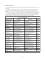
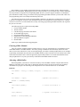
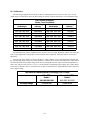
Table 1-1 lists the factory settings of the user-configurable jumpers and switch on the DM5416 module.
Figure 1-1 shows the module layout and the locations of the factory-set jumpers. The following paragraphs explain
how to change the factory settings. Pay special attention to the setting of S1, the base address switch, to avoid
address contention when you first use your module in your system.
Table 1-1: Factory Settings
Switch/
Jumper
P3
Factory Settings
(Jumpers Installed)
Function Controlled
Connects a software selectable or digital interrupt source
to an interrupt channel; pulls tri-state buffers to ground Jumper installed on G (ground for
(G) for multiple interrupt applications
buffer); interrupt channels disabled
P4
Selects the signal available at P2, pin 43
P5
Selects single-ended or differential analog input type
P6
P9
Sets the clock source for User TC Counters 0 & 1
Activates pull-up/ pull-down resistors on Port 0 digital
I/O lines
Activates pull-up/ pull-down resistors on Port 1 digital
I/O lines
Sets the DMA request (DRQ) and DMA acknowledge
(DACK) channel
OT1 (User TC, Counter 1)
Single-ended (jumpers installed on
three S pins)
Counter 0: OSC; Counter 1: OT0
(timer/counters cascaded)
All bits pulled up (jumpers installed
between COM & V)
All bits pulled up (jumpers installed
between COM & V)
Disabled (DMA channel not
selected)
S1
Sets the base address
300 hex (768 decimal)
P7
P8
Fig. 1-1 — Module Layout Showing Factory-Configured Settings
1-3
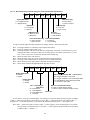
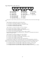
P3 — Interrupt Channel Select (Factory Setting: Jumper G; Interrupt Channel Disabled)
This header connector, shown in Figure 1-2, lets you connect any one of eight software selectable or two
Advanced Digital Interrupt sources to an interrupt channel, IRQ2 (highest priority channel) through IRQ7 (lowest
priority channel). To activate a channel, you must install a jumper vertically across the desired IRQ channel’s pins.
Figure 1-2a shows the factory setting; Figure 1-2b shows the interrupt source connected to IRQ3.
This module supports an interrupt sharing mode where the pins labeled G connect a 1 kilohm pull-down
resistor to the output of a high-impedance tri-state driver which carries the interrupt request signal. This pull-down
resistor drives the interrupt request line low whenever interrupts are not active. When an interrupt request is made,
the tri-state buffer is enabled, forcing the output high and generating an interrupt. There are two IRQ circuits, one
for the software selectable interrupts and one for the digital interrupts. Their outputs are tied together as shown in
Figure 1-3, allowing both interrupt sources to share the same IRQ channel. To determine which circuit has
generated an interrupt on the selected IRQ channel, read the status byte (I/O address location BA + 0) and check
the status of bits 6 and 7, as described in Chapter 4. After the interrupt has been serviced, you must return the IRQ
line low, disabling the tri-state buffer and pulling the output low again. This is done by clearing the software
selectable IRQ at BA + 12, or by clearing the digital IRQ at BA + 6, depending on which source generated the
interrupt. You also can have two or more modules that share the same IRQ channel. You can tell which module
issued the interrupt request by monitoring each module’s IRQ status bit(s). If you are not planning on sharing
interrupts or if you are not sure that your CPU supports interrupt sharing, it is best to disable this feature and use
the interrupts in the normal mode. This will insure compatibility with all CPUs. See chapter 4 for details on
disabling the interrupt sharing circuit.
NOTE: When using multiple modules sharing the same interrupt, only one module should have the G
jumper installed. The rest should be disconnected. Whenever you operate a single module, the G jumper should be
installed. Whenever you operate the module with interrupt sharing disabled, the G jumper should be removed.
P3
Fig. 1-2a:
Factory Setting
Fig. 1-2b:
IRQ3 Selected
Fig. 1-2 — Interrupt Channel Select Jumper, P3
SOFTWARE
SELECTABLE
INTERRUPT
SOURCE
SOFTWARE
SELECTABLE
IRQ STATUS
(BA+0, BIT 6)
CLK
INTERRUPT
REGISTER
+5 V
INTERRUPT
CLR
CLR
DIGITAL
INTERRUPT
SOURCE
P3
G
DIGITAL
IRQ STATUS
(BA+0, BIT 7)
CLK
INTERRUPT
REGISTER
+5 V
CLR
CLR
Fig. 1-3 — Pulling Down the Interrupt Request Lines
1-4
2
3
4
5
6
7
G
2
3
4
5
6
7
G
P3
P4 — P2, Pin 43 Signal Select (Factory Setting: OT1)
This header connector, shown in Figure 1-4, lets you select the output signal from the module that is present
at I/O connector P2, pin 43. You can select the output from the User TC Counter 1 or the digital interrupt. User
P4
OT1
DIG
Fig. 1-4 — P2, Pin 43 Signal Select Jumper, P4
TC Counter 1 is labeled OT1 on this header, and the digital interrupt is labeled DIG.
P5 — Single-Ended/Differential Analog Inputs (Factory Setting: Single-Ended)
This header connector, shown in Figure 1-5, configures the DM5416 for 16 single-ended or 8 differential
analog input channels. When operating in the single-ended mode, three jumpers must be installed across the S
pins. When operating in the differential mode, the jumpers must be installed across the D pins. DO NOT install
S
D
S
D
S
D
P5
Fig. 1-5 — Single-Ended/Differential Analog Input Signal Type Jumpers, P5
jumpers across both S and D pins at the same time!
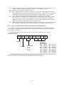
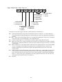
P6 — User TC Clock Source Select (Factory Settings: Counter 0: OSC, Counter 1: OT0)
This header connector, shown in Figure 1-6, lets you select the clock sources for User TC Counters 0 and 1,
the 16-bit timer/counters available for user functions. Figure 1-7 shows a block diagram of the User TC circuitry
to help you in making these connections.
The clock source for Counter 0 is selected by placing a jumper on one of the three rightmost pairs of pins on
the header, OSC, ECK, or EPC. OSC is the on-board 8 MHz clock; ECK is an external clock source which can be
connected through I/O connector P2, pin 45; and EPC is an external pacer clock which can be connected through I/O
connector P2, pin 41.
The four leftmost pins, OT0, OSC, ECK, and EPC, set the clock source for timer/counter Counter 1. OT0 is the
output of Counter 0; OSC is the on-board 8 MHz clock; ECK is an external clock source which can be connected
through I/O connector P2, pin 45; and EPC is an external pacer clock which can be connected through I/O connector
P6
OSC
ECK
EPC
OT0
OSC
ECK
EPC
Fig. 1-6 — User TC Clock Sources Jumpers, P6
1-5
5416
I/O CONNECTOR
P2
P6
U9
OSC
CLK
COUNTER
0
8 MHz
ECK
PIN 45
EXT CLK
EPC
PIN 41
EXT PCLK / STRB IN
PIN 46
EXT GATE 0
PIN 44
T/C OUT 0
PIN 42
EXT GATE 1
PIN 43
T/C OUT 1 / DIG IRQ
+5 V
GATE
OUT
OT0
OSC
8 MHz
ECK
EPC
TO TRIGGER CIRCUIT
TO DIGITAL CHIP
CLK
COUNTER
1
+5 V
GATE
P4
OUT
OT1
DINT
DIGITAL INTERRUPT
LOAD SAMPLE COUNT
CLK
COUNTER
2
A/D TRIGGER
GATE
+5 V
OUT
SAMPLE COUNT
Fig. 1-7 — User TC Circuit Diagram
P2, pin 41. Counters 0 and 1 are factory set as a 32-bit cascaded counter clocked by the 8 MHz system clock.
P9 — DMA Request/DMA Acknowledge Channel (Factory Setting: Disabled)
This header connector, shown in Figure 1-8, lets you select channel 1 or channel 3 for DMA transfers. Both
the DMA request (DRQ) and DMA acknowledge (DACK) lines must be jumpered for the same channel. This is
done by placing a jumper across the selected DRQ channel and a jumper across the same DACK channel. The
factory setting is disabled, as shown in Figure 1-3a. Figure 1-3b shows the module set for DMA transfers on
channel 1. Note that if any other device in your system is already using the DMA channel you select, channel
1
3
1
3
1
3
1
3
DRQ DACK P9
DRQ DACK P9
Fig. 1-3b: DMA Channel 1
Selected
Fig. 1-3a:
Factory Setting
Fig. 1-8 — DMA Request/DMA Acknowledge Channel Jumper, P9
1-6
contention will result, causing erratic operation.
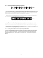
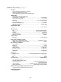
S1 — Base Address (Factory Setting: 300 hex (768 decimal))
One of the most common causes of failure when you are first trying your module is address contention. Some
of your computer’s I/O space is already occupied by internal I/O and other peripherals. When the module attempts
to use I/O address locations already used by another device, contention results and the module does not work.
To avoid this problem, the DM5416 has an easily accessible DIP switch, S1, which lets you select any one of
32 starting addresses in the computer’s I/O. Should the factory setting of 300 hex (768 decimal) be unsuitable for
your system, you can select a different base address simply by setting the switches to any one of the values listed
in Table 1-2. The table shows the switch settings and their corresponding decimal and hexadecimal (in parentheses) values. Make sure that you verify the order of the switch numbers on the switch (1 through 5) before setting
them. When the switches are pulled forward, they are OPEN, or set to logic 1, as labeled on the DIP switch
Fig. 1-9 — Base Address Switch, S1
Table 1-2: Base Address Switch Settings, S1
Base Address
Decimal / (Hex)
Switch Setting
5 4 3 2 1
Base Address
Decimal / (Hex)
Switch Setting
5 4 3 2 1
512 / (200)
0 0 0 0 0
768 / (300)
1 0 0 0 0
528 / (210)
0 0 0 0 1
784 / (310)
1 0 0 0 1
544 / (220)
0 0 0 1 0
800 / (320)
1 0 0 1 0
560 / (230)
0 0 0 1 1
816 / (330)
1 0 0 1 1
576 / (240)
0 0 1 0 0
832 / (340)
1 0 1 0 0
592 / (250)
0 0 1 0 1
848 / (350)
1 0 1 0 1
608 / (260)
0 0 1 1 0
864 / (360)
1 0 1 1 0
624 / (270)
0 0 1 1 1
880 / (370)
1 0 1 1 1
640 / (280)
0 1 0 0 0
896 / (380)
1 1 0 0 0
656 / (290)
0 1 0 0 1
912 / (390)
1 1 0 0 1
672 / (2A0)
0 1 0 1 0
928 / (3A0)
1 1 0 1 0
688 / (2B0)
0 1 0 1 1
944 / (3B0)
1 1 0 1 1
704 / (2C0)
0 1 1 0 0
960 / (3C0)
1 1 1 0 0
720 / (2D0)
0 1 1 0 1
976 / (3D0)
1 1 1 0 1
736 / (2E0)
0 1 1 1 0
992 / (3E0)
1 1 1 1 0
752 / (2F0)
0 1 1 1 1
1008 / (3F0)
1 1 1 1 1
0 = closed, 1 = open
1-7
package. When you set the base address for your module, record the value in the table inside the back cover.
Figure 1-9 shows the DIP switch set for a base address of 300 hex (768 decimal).
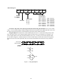
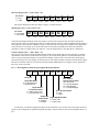
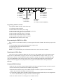
P7 and P8, Pull-up/Pull-down Resistors on Digital I/O Lines
The DM5416 has 16 TTL/CMOS compatible digital I/O lines which can be interfaced with external devices.
These lines are divided into two groups: Port 0 with eight individual bit programmable lines, and Port 1 with eight
port programmable lines. You can connect pull-up or pull-down resistors to any or all of these lines on a bit by bit
basis. You may want to pull lines up for connection to switches. This will pull the line high when the switch is
disconnected. Or, you may want to pull lines down for connection to relays which control turning motors on and off.
These motors turn on when the digital lines controlling them are high. By pulling these lines down, you can ensure
that when the data acquisition system is first turned on, the motors will not switch on before the port is initialized.
Pull-up/pull-down resistors are installed on the module, and jumpers are installed in the pull-up position on P7
and P8 for all 16 I/O lines. Each bit is labeled on the module. P7 connects to the resistors for Port 0 and P8 connects
to the resistors for Port 1. The pins are labeled G (for ground) on one end and V (for +5V) on the other end. The
middle pin is common. Figure 1-10 shows these headers with the factory-installed jumpers, with the jumpers placed
between the common pin (middle pin of the three) and the V pin. For pull-downs, install the jumper across the
common pin (middle pin) and G pin. To disable the pull-up/pull-down resistor, remove the jumper.
P7
Fig. 1-10 — Ports 0 and 1 Pull-up/Pull-down Resistor Connections
1-8
PORT 1
Fig. 1-10b:
P8 - Port 1 Bits
0
1
2
Fig. 1-10a:
P7 - Port 0 Bits
3
P8
4
G
5
G
PORT 0
6
V
7
0
1
2
3
4
5
6
7
V
CHAPTER 2
INSTALLATION
The DM5416 is easy to install in your cpuModule™ or other
PC/104 based system. This chapter tells you step-by-step how to
connect the module.
After you have made all of your connections, you can turn your
system on and run the 5416DIAG board diagnostics program
included on your example software disk to verify that the module
is working.
2-1
2-2
Installation
Keep the module in its antistatic bag until you are ready to install it in your cpuModule™ or other PC/104 based
system. When removing it from the bag, hold the module at the edges and do not touch the components or connectors.
Before installing the module in your system, check the jumper and switch settings. Chapter 1 reviews the
factory settings and how to change them. If you need to change any settings, refer to the appropriate instructions in
Chapter 1. Note that incompatible jumper settings can result in unpredictable module operation and erratic response.
TheDM5416 comes with a stackthrough P1 connector. The stackthrough connector lets you stack another
module on top of your DM5416.
To install the module, follow the procedures described in the computer manual and the steps below:
1. Turn OFF the power to your system.
2. Touch a metal rack to discharge any static buildup and then remove the module from its antistatic bag.
3. Select the appropriate standoffs for your application to secure the module when you install it in your system
(two sizes are included with the module).
4. Holding the module by its edges, orient it so that the P1 bus connector’s pin 1 lines up with pin 1 of the
expansion connector onto which you are installing the module.
5. After carefully positioning the module so that the pins are lined up and resting on the expansion connector,
gently and evenly press down on the module until it is secured on the connector.
NOTE: Do not force the module onto the connector. If the module does not readily press into place, remove
it and try again. Wiggling the module or exerting too much pressure can result in damage to the DM5416 or
to the mating module.
6. After the module is installed, connect the cable to I/O connector P2 on the module. When making this
connection, note that there is no keying to guide you in orientation. You must make sure that pin 1 of the
cable is connected to pin 1 of P2 (pin 1 is marked on the module with a small square). For twisted pair
cables, pin 1 is the dark brown wire; for standard single wire cables, pin 1 is the red wire.
7. Make sure all connections are secure.
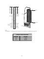
External I/O Connections
Figure 2-1 shows the DM5416’s P2 I/O connector pinout. Refer to this diagram as you make your I/O connections. Note that +12 volts at pin 47 and -12 volts at pin 49 are available only if your computer bus supplies them
(these voltages are not provided by the module).
2-3
DIFF.
S.E.
DIFF.
S.E.
AIN1+
AIN1
1
2
AIN1-
AIN2+
AIN2
3
4
AIN2-
AIN10
AIN3+
AIN3
5
6
AIN3-
AIN11
AIN4+
AIN4
7
8
AIN4-
AIN12
AIN4+
AIN5
9
10
AIN5-
AIN13
AIN6+
AIN6
11 12
AIN6-
AIN14
AIN7+
AIN7
13 14
AIN7-
AIN15
AIN8+
AIN8
15 16
AIN8-
AIN16
AOUT 1
17 18
ANALOG GND
AIN9
N.C.
19 20
ANALOG GND
ANALOG GND
21 22
ANALOG GND
P0.7
23 24
P1.7
P0.6
25 26
P1.6
P0.5
27 28
P1.5
P0.4
29 30
P1.4
P0.3
31 32
P1.3
P0.2
33 34
P1.2
P0.1
35 36
P1.1
P0.0
37 38
P1.0
TRIGGER IN
39 40
DIGITAL GND
EXT PCLK / STRB IN
41 42
EXT GATE 1
T/C OUT 1 / DIG IRQ
43 44
T/C OUT 0
EXT CLK
45 46
EXT GATE 0
+12 VOLTS
47 48
+5 VOLTS
-12 VOLTS
49 50
DIGITAL GND
Fig. 2-1 — P2 I/O Connector Pin Assignments
Connecting the Analog Input Pins
The analog inputs on the module can be set for single-ended or differential operation.
NOTE: It is good practice to connect all unused channels to ground, as shown in the following diagrams.
Failure to do so may affect the accuracy of your results.
Single-Ended. When operating in the single-ended mode, connect the high side of the analog input to one of
the analog input channels, AIN1 through AIN16, and connect the low side to an ANALOG GND (pins 18 and 20-22
on P2). Figure 2-2 shows how these connections are made.
Differential. When operating in the differential mode, twisted pair cable is recommended to reduce the effects
of magnetic coupling at the inputs. Your signal source may or may not have a separate ground reference. When
using the differential mode, you should install a 10 kilohm resistor pack at location RN1 on the module to provide a
reference to ground for signal sources without a separate ground reference.
First, connect the high side of the analog input to the selected analog input channel, AIN1+ through AIN8+, and
connect the low side of the input to the corresponding AIN- pin. Then, for signal sources with a separate ground
reference, connect the ground from the signal source to an ANALOG GND (pins 18 and 20-22 on P2). Figure 2-3
shows how these connections are made.
2-4
I/O CONNECTOR
P2
SIGNAL
SOURCE
1 OUT
+
PIN 1
AIN 1
GND
MUX
SIGNAL
SOURCE
15 OUT
+
PIN 14
OUT +
+
OUT -
-
AIN 15
GND
PIN 16
AIN 16
PIN 22
Fig. 2-2 — Single-Ended Input Connections
I / O C O N N E C TO R
P2
SIGNAL
+
SOURCE
1 OUT
PI N 1
-
PI N 2
AI N 1+
RN1
AI N 110K
MUX
SIGNAL
+
SOURCE
7 OUT
PI N 13
-
PI N 14
OUT +
+
OUT -
-
AI N 7+
AI N 710K
GND
PI N 15
AI N 8+
PI N 16
10K
AI N 8-
PI N 22
Fig. 2-3 — Differential Input Connections
2-5
Connecting the Module for Simultaneous Sampling
Multiple modules can be sampled simultaneously by connecting an external trigger source to the TRIGGER IN
pin, P2-39, and an external pacer clock to the EXT PCLK pin, P2-41, of each module. Figure 2-4 shows to make
these connections.
When applying an external trigger to a module’s TRIGGER IN pin, note that the trigger polarity and external
trigger repeat bits must be configured as desired at the BA +2, Trigger 1 Register, and the external trigger must be
programmed as the start trigger source at the BA + 2, Trigger 0 Register. The external trigger pulse duration should
be at least 100 nanoseconds.
For simultaneous sampling, you must connect the same clock source to each module so that conversions are
synchronized. This is accomplished by connecting the same external pacer clock to EXT PCLK, as shown on Figure
2-4 and selecting the external pacer clock at bit 0 in the Trigger 1 Register programmed at BA + 2. The trigger will
start the pacer clock, and the pacer clock will simultaneously start conversions on all modules. After the pacer clock
starts, the sampling uncertainty in is less than 5 nanoseconds.
I/O CONNECTOR
P2
BOARD #1
MUX
SIGNAL
SOURCE
1 OUT
+
EXTERNAL
PACER CLOCK
EXTERNAL
TRIGGER
CH 1
PIN 1
CH 1
PIN 2
AIN1 +
AIN1 -
RN1
10K
PIN 41
EXT PCLK
PIN 39
TRIGGER IN
BOARD #2
MUX
SIGNAL
SOURCE
2 OUT
+
-
PIN 1
CH 1
AIN1 +
PIN 2
CH 1
RN1
10K
AIN1 -
PIN 39
TRIGGER IN
PIN 41
EXT PCLK
Fig. 2-4 — Two Modules Configured for Simultaneous Sampling
Connecting the Analog Output (-2 Module)
For the D/A output, connect the high side of the device receiving the output to the AOUT1 channel (P2-17) and
connect the low side of the device to an ANALOG GND (P2-18 or P2-20).
Connecting the Timer/Counters and Digital I/O
For all of these connections, the high side of an external signal source or destination device is connected to the
appropriate signal pin on the I/O connector, and the low side is connected to any DIGITAL GND.
Running the 5416DIAG Diagnostics Program
Now that your module is ready to use, you will want to try it out. An easy-to-use, menu-driven diagnostics
program, 5416DIAG, is included with your example software to help you verify your module’s operation. Note that
the diagnostics program takes several A/D readings and averages these readings for the most accurate results. You
can also use this program to make sure that your current base address setting does not contend with another device.
2-6
CHAPTER 3
HARDWARE DESCRIPTION
This chapter describes the features of the DM5416 hardware.
The major circuits are the A/D, the D/A, the timer/counters, and
the digital I/O lines.
3-1
3-2
The DM5416 has four major circuits, the A/D, the D/A, the timer/counters, and the digital I/O lines. Figure 3-1
shows the block diagram of the module. This chapter describes the hardware which makes up the major circuits.
CHANNEL / GAIN
SCAN MEMORY
AND CONTROL
DATA
DMA
CONTROL
AND
SELECT
FIFO
1024 X 16
PROGRAMMABLE
GAIN
AMPLIFIER
1/2/4/8
16-BIT
A/D
CONVERTER
16
MUX
16 ANALOG INPUTS
8 DIFF./16 S.E.
-10V TO +10V
HIGH SPEED SAMPLE
COUNTER
PACER/
BURST
CLOCK
TRIGGER
CONTROL
TRIGGER IN
EXT PACER CLK
8 MHz
OSC
8254
PIT
TIMER
I/O
SELECT
6
5
TIMER I/O
8
ADDRESS
ADDRESS
DECODE
CONTROL
PULL-UP/DOWN
RESISTORS
MUX
P1.0 - P1.7
8
P0.0 - P0.7
8
I/O CONNECTOR
PC BUS
INTERRUPT
SELECT
8
DIGITAL
I/O
EVENT/MATCH
INTERRUPT
16-BIT
D/A
CONVERTER
-10V to +10V
+5 VOLTS
±12 VOLTS
DC/DC
CONVERTER
CONTROL
±15 VOLTS
±12 VOLTS
+5 VOLTS
Fig. 3-1 — DM5416 Block Diagram
A/D Conversion Circuitry
The DM5416 performs analog-to-digital conversions on up to 8 differential or 16 single-ended softwareselectable analog input channels. The following paragraphs describe the A/D circuitry.
Analog Inputs
The input voltage range is -10 to +10 volts. Software-programmable binary gains of 1, 2, 4, and 8 let you
amplify lower level signals to more closely match the module’s input ranges. Overvoltage protection to ±35 volts is
provided at the inputs.
Channel-gain Scan Memory
The channel-gain scan memory lets you sample channels in any order, at high speeds, with a different gain on
each channel. This 1024 x 16-bit memory supports complex channel-gain scan sequences, including digital output
control. Using the digital output control feature, you can control external input expansion boards such as the MX32
to expand channel capacity to up to 512 channels. When used, these control lines are output on Port 1. When the
digital lines are not used for this feature, they are available for other digital control functions.
3-3
A skip bit is provided in the channel-gain data word to support different sampling rates on different channels.
When this bit is set, no A/D conversion is performed on the selected channel. Chapters 4 and 5 detail this feature.
A/D Converter
The 16-bit successive approximation A/D converter accurately digitizes dynamic input voltages in 10 microseconds, for a maximum throughput rate of 100 kHz and a resolution of 0.3 millivolts for a gain of 1. The converter
chip contains a sample-and-hold amplifier, a 16-bit A/D converter, a 5-volt reference, a clock, and a digital interface
to provide a complete high resolution A/D conversion function on a single chip. Its low power CMOS logic combined with a high precision, low noise design give you accurate results.
Conversions are controlled by software command, by pacer clock, by using triggers to start and stop sampling,
or by the sample counter to acquire a specified number of samples. An on-board or external pacer clock can be used
to control the conversion rate. Conversion modes are described in Chapter 5, A/D Conversions.
1024 Sample Buffer
A first in, first out (FIFO) 1024 sample buffer helps your computer manage the high throughput rate of the A/D
converter by providing an elastic storage bin for the converted data. Even if the computer does not read the data as
fast as conversions are performed, conversions will continue until a FIFO full flag is sent to stop the converter.
The sample buffer does not need to be addressed when you are writing to or reading from it; internal addressing
makes sure that the data is properly stored and retrieved. All data accumulated in the sample buffer is stored intact
until the PC is able to complete the data transfer. Its asynchronous operation means that data can be written to or
read from it at any time, at any rate. When a transfer does begin, the data first placed in the FIFO is the first data out.
Data Transfer
The converted data can be transferred to PC memory in one of three ways. Direct memory access (DMA)
transfer supports conversion rates of up to 100,000 samples per second. Data also can be transferred using the
programmed I/O mode or the interrupt mode. A special interrupt mode using a REP INS (Repeat Input String)
instruction supports very high speed data transfers. By generating an interrupt when the FIFO’s half full flag is set, a
REP INS instruction can be executed, transferring data to PC memory and emptying the sample buffer at the
maximum rate allowed by the data bus.
The PC data bus is used to read and/or transfer data to PC memory. In the DMA transfer mode, you can make
continuous transfers directly to PC memory without going through the processor.
The converted data is stored in the 16-bit data word written to the sample buffer. The data is read in two bytes,
the LSB followed by the MSB.
D/A Converter (-2 Module)
A 16-bit analog output channel is included on the DM5416-2. The analog output is generated by a 16-bit D/A
converter with an output range of -10 to +10 volts, and a resolution of 0.3 millivolts.
Timer/Counters
Two 8254 programmable interval timers provide six 16-bit, 8-MHz timer/counters to support a wide range of
timing and counting functions. The 8254 at U10 is the Clock TC. Two of its 16-bit timer/counters, Counter 0 and
Counter 1, are cascaded and reserved for the pacer clock. The pacer clock is described in Chapter 5. The third timer/
counter in the Clock TC, Counter 2, is the burst clock. Figure 3-2 shows the Clock TC circuitry.
The 8254 at U9 is the User TC. On the User TC, Counters 0 and 1 are available to the user. Counter 2 is the
sample counter. Figure 3-3 shows the User TC circuitry.
Each 16-bit timer/counter has two inputs, CLK in and GATE in, and one output, timer/counter OUT. Each can
be programmed as binary or BCD down counters by writing the appropriate data to the command word, as described
in Chapter 4. The command word also lets you set up the mode of operation. The six programmable modes are:
3-4
Mode 0
Mode 1
Mode 2
Mode 3
Mode 4
Mode 5
Event Counter (Interrupt on Terminal Count)
Hardware-Retriggerable One-Shot
Rate Generator
Square Wave Mode
Software-Triggered Strobe
Hardware Triggered Strobe (Retriggerable)
These modes are detailed in the 8254 Data Sheet, reprinted from Intel in Appendix C.
U10
8 MHz (OSC)
CLK
COUNTER
0
PACER CLOCK
GATE CONTROL
GATE
OUT
CLK
COUNTER
1
16-BIT PACER CLOCK
GATE
COUNTER
2
OUT
32-BIT PACER CLOCK
CLK
8 MHz (OSC)
BURST GATE CONTROL
GATE
BURST CLOCK
OUT
Fig. 3-2 — Clock TC Circuit Block Diagram
5416
I/O CONNECTOR
P2
P6
U9
OSC
CLK
COUNTER
0
8 MHz
ECK
PIN 45
EXT CLK
EPC
PIN 41
EXT PCLK / STRB IN
PIN 46
EXT GATE 0
PIN 44
T/C OUT 0
+5 V
GATE
OUT
OT0
OSC
8 MHz
ECK
EPC
TO TRIGGER CIRCUIT
TO DIGITAL CHIP
CLK
COUNTER
1
+5 V
GATE
P4
OUT
PIN 42
EXT GATE 1
PIN 43
T/C OUT 1 / DIG IRQ
OT1
DINT
DIGITAL INTERRUPT
LOAD SAMPLE COUNT
CLK
COUNTER
2
GATE
A/D TRIGGER
+5 V
OUT
SAMPLE COUNT
Fig. 3-3 — User TC Circuit Block Diagram
3-5
Digital I/O
The 16 digital I/O lines can be used to transfer data between the computer and external devices. Eight lines are
bit programmable and eight lines are byte, or port, programmable.
Port 0 provides eight bit programmable lines which can be independently set for input or output. Port 0 supports
RTD’s two Advanced Digital Interrupt modes. An interrupt can be generated when the lines match a programmed
value or when any bit changes its current state. A Mask Register lets you monitor selected lines for interrupt
generation.
Port 1 can be programmed as an 8-bit input or output port.
Chapter 10 details digital I/O operations and Chapter 7 explains digital interrupts.
3-6
CHAPTER 4
I/O MAPPING
This chapter provides a complete description of the I/O map for
the DM5416, general programming information, and how to set
and clear bits in a port.
4-1
4-2
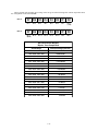
Defining the I/O Map
The I/O map for the DM5416 is shown in Table 4-1 below. As shown, the module occupies 16 consecutive I/O
port locations.
To conserve the use of I/O space, the structure of the I/O map is such that some of the registers control what
operation you are performing at other addresses. The control register at BA + 0 selects which registers you are
talking to at BA + 1, BA + 2, BA + 3, and BA + 8 through BA + 11. The digital register you address at BA + 6 is
selected at BA + 7. This scheme is easily understood as you review the register descriptions on the following pages.
The base address (designated as BA) can be selected using DIP switch S1, located on the edge of the module,
as described in Chapter 1, Module Settings. This switch can be accessed without removing the module from the
stack. The following sections describe the register contents of each address used in the I/O map.
Table 4-1: DM5416 I/O Map
Address *
(Decimal)
Register Description
Read Function
Read Board Status/Set
Control Register/Clear
Read board status word
Start Convert/Load
Channel-Gain Data
Start Convert
Read LSB/Set Trigger Modes
& IRQ Source
Read bottom 8 bits of converted data
Write Function
Program DM5416 control register and
clear operations
Load channel & gain; load A/D & digital
bytes into channel-gain table
Set up triggers, clocks & IRQ source
(dependent on BA + 0)
Read MSB/Clear Settings
Digital I/O Port 0
(Bit Programmable)
Digital I/O Port 1
(Port Programmable)
Read top 8 bits of converted data
Clear settings (dependent on BA + 0)
BA + 3
Read Port 0 digital input lines
Program Port 0 digital output lines
BA + 4
Read Port 1 digital input lines
Clear digital IRQ status flag/read Port 0
direction, mask or compare register
(dependent on BA + 7)
Program Port 1 digital output lines
Clear digital chip/program Port 0
direction, mask or compare register
(dependent on BA + 7)
Program digital control register & digital
interrupt enable
BA + 5
Port 0 Clear/
Direction/Mask/Compare
Read Digital I/O Status/
Set Digital Control Register
8254 Clock TC Counter 0 &
User TC Counter 0
8254 Clock TC Counter 1 &
User TC Counter 1
8254 Clock TC Counter 2 &
User TC Counter 2
8254 Clock TC & User TC
Control Word
Clear IRQ/
D/A Converter 1 LSB
Clear DMA Done/
D/A Converter 1 MSB
Read digital status word
Read value in Clock or User TC
Counter 0 (dependent on BA + 0)
Read value in Clock or User TC
Counter 1 (dependent on BA + 0)
Read value in Clock or User TC
Counter 2 (dependent on BA + 0)
Reserved
Clear software selectable IRQ status
flag
Load count in Clock or User TC Counter
0 (dependent on BA + 0)
Load count in Clock or User TC Counter
1 (dependent on BA + 0)
Load count in Clock or User TC Counter
2 (dependent on BA + 0)
Program counter mode for Clock or
User TC (dependent on BA + 0)
Program DAC1 LSB (-2 version)
BA + 0
BA + 1
BA + 2
BA + 6
BA + 7
BA + 8
BA + 9
BA + 10
BA + 11
BA + 12
BA + 13
Initialize Sample Counter
Clear DMA done flag
Program DAC1 MSB (-2 version)
Provides software trigger to load sample
counter
Reserved
Update DAC
Update D/A converter output
BA + 15
Reserved
* BA = Base Address
4-3
BA + 14
BA + 0: Read Status/Program Control Register and Clear Functions (Read/Write)
D7 D6 D5 D4 D3 D2 D1 D0
FIFO Empty Flag
0 = FIFO empty
1 = FIFO not empty
Digital IRQ Status
0 = no digital interrupt
1 = digital interrupt
IRQ Status
0 = no interrupt
1 = interrupt
FIFO Full Flag
0 = FIFO full
1 = FIFO not full
Halt Flag
0 = A/D enabled
1 = A/D disabled
DMA Done Flag
0 = DMA not done
1 = DMA done
Pacer Clock Gate Flag
0 = pacer clock off
1 = pacer clock on
End-of-Convert Status
0 = converting
1 = not converting
A read provides the eight status bits defined below. Starting with bit 0, these status bits show:
Bit 0 – Goes high when there is something in the sample buffer (FIFO).
Bit 1 – Goes low when the sample buffer is full.
Bit 2 – Goes high and halts A/D conversions when the sample buffer is full (this is useful whenever you are
emptying the buffer at a slower rate than you are taking data). A clear FIFO written to BA + 3 (with
BA + 0, bits 1 and 0 set to 00) clears the sample buffer and this flag.
Bit 3 – Shows the status of the A/D converter.
Bit 4 – Shows the status of the pacer clock (useful when using external triggering).
Bit 5 – Goes high when a DMA transfer is completed (active in DMA mode only).
Bit 6 – Shows when one of the eight software selectable interrupts has occurred.
Bit 7 – Shows when an Advanced Digital Mode interrupt has occurred.
D7 D6 D5 D4 D3 D2 D1 D0
Enable Digital Table
0 = disable
1 = enable
BA + 2 Register Select / BA + 3 Clear Select
00 = Trigger 0 Register / clear FIFO
01 = Trigger 1 Register / clear channel-gain table
10 = IRQ Register / reset channel-gain table
11 = reserved / clear board
Enable A/D Table
0 = disable
1 = enable
BA + 1 Channel-gain
Load Select
00 = load latches
01 = load A/D table
10 = load digital table
11 = reserved
BA + 8-11 Timer/Counter Select
0 = Clock TC (pacer & burst clocks)
1 = User TC (user counters & sample counter)
Reserved
A write to BA + 0 sets up a Control Register. The settings you enter here determine which register you address
at BA + 2, which clear operation is carried out by a write to BA + 3, which timer/counter you address at BA + 8
through BA + 11, and what operations you perform on the channel-gain table at BA + 1. This register sets:
Bits 0 and 1 – Selects the register you talk to at BA + 2, where triggers, clocks, and interrupts are set, and the
clear operation to be performed by a write to BA + 3. These registers and clear functions are described
at addresses BA + 2 and BA + 3.
4-4
Bit 2 – Selects the 8254 timer/counter to be programmed at BA + 8 through BA + 11. The Clock TC (U11) is
the pacer clock/burst clock timer, and User TC (U10) is the user/sample counter timer.
Bit 3 – Reserved. The value written to this bit is ignored.
Bits 4 and 5 – When bits 5 and 4 are set to 00, a write at BA + 1 writes the 8-bit channel-gain data to the onboard latches which form the Channel/Gain Register. When set to 01, a write at BA + 1 enters the 8-bit
channel-gain data into the A/D Table in the channel-gain scan memory. When set to 10, a write at
BA + 1 enters the 8-bit digital data into the Digital Table in the channel-gain scan memory.
Bit 6 – When enabled, the A/D portion of the channel-gain table is activated to be used for A/D conversions.
Note that while you can enable, disable, and then re-enable the channel-gain table in the middle of
taking a set of data, it is not recommended that you do this. One entry in the table is skipped each time
the table is stopped and restarted during the same sampling session.
Bit 7 – When enabled, the digital portion of the channel-gain table is activated to be used with A/D conversions.
This portion of the channel-gain table cannot be enabled without enabling the A/D portion (bit 6).
BA + 1: Start Convert/Channel & Gain Select/Load Channel-gain Table (Read/Write)
The registers at this address are used to load channel and gain information directly to the channel and gain
latches or into the A/D portion of the channel-gain table, to load digital information into the digital table, and to
issue a start convert command.
To start a conversion: A read at this address issues a Start Convert command (software trigger).
Channel/Gain Register:
D7 D6 D5 D4 D3 D2 D1 D0
Reserved
Reserved
Channel Gain
00 = x1
01 = x2
10 = x4
11 = x8
Analog Input
Channel Select
0000 = channel 1
0001 = channel 2
0010 = channel 3
0011 = channel 4
0100 = channel 5
0101 = channel 6
0110 = channel 7
0111 = channel 8
1000 = channel 9
1001 = channel 10
1010 = channel 11
1011 = channel 12
1100 = channel 13
1101 = channel 14
1110 = channel 15
1111 = channel 16
To load channel and gain for conversions not using the channel-gain table: First, make sure that bits 5 and
4 at BA + 0 are set to 00. Then write the desired channel and gain information to BA + 1.
4-5
A/D Table Register:
D7 D6 D5 D4 D3 D2 D1 D0
Skip Bit
0 = disabled
1 = enabled
Analog Input
Channel Select
0000 = channel 1
0001 = channel 2
0010 = channel 3
0011 = channel 4
0100 = channel 5
0101 = channel 6
0110 = channel 7
0111 = channel 8
Channel Gain
00 = x1
01 = x2
10 = x4
11 = x8
Reserved
1000 = channel 9
1001 = channel 10
1010 = channel 11
1011 = channel 12
1100 = channel 13
1101 = channel 14
1110 = channel 15
1111 = channel 16
To load the A/D portion of the channel-gain table with channel and gain information: First, set bits 5 and 4
at BA + 0 to 01 to enable loading of channel and gain data into the A/D portion of the channel-gain table. Then, load
the data in the format shown above. Each load fills the next position in the channel-gain table.
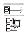
Using the skip bit: The skip bit at bit 7 of the channel-gain word is set to 1 if you want to skip an entry in the
table. This feature allows you to sample multiple channels at different rates on each channel. For example, if you
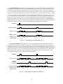
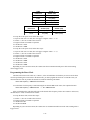
want to sample channel 1 once each second and channel 4 once every 3 seconds, you can set the skip bit on channel 4 as shown in Figure 4-1. With the skip bit set on the four table entries as shown, these entries will be ignored,
and no A/D conversion will be performed. This saves memory and eliminates the need to throw away unwanted
data.
Pacer Clock
1 sec
A/D Conversion
Channel
Sampled
1
1
1
1 sec
1 sec
1 sec
1 sec
4
1
4 skip
1
4 skip
1
4
1
4 skip
1
4 skip
1
4
1
1
3 sec
Fig. 4-1 — Using the Skip Bit
4-6
1
4
Digital Table Register:
D7 D6 D5 D4 D3 D2 D1 D0
MX32 Channel Select
00000 = channel 1
00001 = channel 2
•
11111 = channel 32
To load the digital portion of the channel-gain table with digital information: The digital portion of the
channel-gain table provides 8 bits to control devices such as external expansion boards. For example, if you have
connected one of your input channels on the DM5416 to RTD’s MX32 input expansion board, you can use the
bottom 5 bits in this byte to control the MX32 board. To load digital information into this portion of the channelgain table, set bits 5 and 4 at BA + 0 to 10 to enable loading of the digital portion of the channel-gain table. Then,
load the data, setting 0’s and 1’s as needed by whatever you are controlling. This information will be output on the
Port 1 lines when you run through the table. The format shown above is for controlling the MX32’s channel selection (32 single-ended or 16 differential). The first load operation will be in the first entry slot of the table (lining up
with the first entry in the A/D table), and each load thereafter fills the next position in the channel-gain table.
BA + 2: Read A/D Data LSB/Program Trigger Modes & IRQ Source (Read/Write)
D7 D6 D5 D4 D3 D2 D1 D0
Bit 7
Bit 6
Bit 5
Bit 4
Bit 3
Bit 2
Bit 1
Bit 0
(LSB)
A read provides the bottom 8 bits of the 16 bits of converted data. The result read here is combined with the
8-bit MSB read at BA + 3 to obtain the entire 16-bit word in twos complement format. Key values are shown in the
table below.
A write to this register programs one of three registers, depending on the setting of bits 0 and 1 at BA + 0.
A/D Converter Bit Weights,
Bipolar, Twos Complement
A/D Bit Weight
Ideal Input Voltage
(millivolts)
A/D Bit Weight
Ideal Input Voltage
(millivolts)
1111 1111 1111 1111
-0.305176
0000 0000 1000 0000
+39.062500
1000 0000 0000 0000
-10000.000000
0000 0000 0100 0000
+19.531250
0100 0000 0000 0000
+5000.000000
0000 0000 0010 0000
+9.775625
0010 0000 0000 0000
+2500.000000
0000 0000 0001 0000
+4.882813
0001 0000 0000 0000
+1250.000000
0000 0000 0000 1000
+2.441406
0000 1000 0000 0000
+625.000000
0000 0000 0000 0100
+1.220703
0000 0100 0000 0000
+312.500000
0000 0000 0000 0010
+0.610352
0000 0010 0000 0000
+156.250000
0000 0000 0000 0001
0000 0001 0000 0000
+78.125000
0000 0000 0000 0000
+0.305176
0.000000
4-7
Trigger 0 Register (BA + 0, bits 1 and 0 = 00):
D7 D6 D5 D4 D3 D2 D1 D0
Stop Trigger Select
000 = software trigger
001 = external trigger
010 = digital interrupt
011 = sample counter
100 = about software trigger
101 = about external trigger
110 = about digital interrupt
111 = about User TC Counter 1 out
Start Trigger Select
000 = software trigger
001 = external trigger
010 = digital interrupt
011 = User TC Counter 1 out
100 = gate mode
101 = reserved
110 = reserved
111 = reserved
Conversion Select
00 = software trigger
01 = pacer clock
10 = burst clock
11 = digital interrupt
This register sets up the method by which A/D conversion are performed (conversion select bits) and the trigger
mode.
Trigger 0 Register, performing A/D conversions (bits 0 and 1):
00 = conversions are controlled by reading BA + 1 (Start Convert).
01 = conversions are controlled by the internal or an external pacer clock.
10 = conversions are controlled by the burst clock.
11 = conversions are controlled by a digital interrupt.
Trigger 0 Register, selecting the start trigger source (bits 2 through 4):
000 = the pacer clock is started by reading BA + 1 (Start Convert).
001 = the pacer clock is started by an external trigger (TRIGGER IN, P2-39).
010 = the pacer clock is started by a digital interrupt.
011 = the pacer clock is started when the output of User TC Counter 1 reaches 0.
100 = the pacer clock runs as long as the TRIGGER IN line is held high or low, depending on the polarity bit
setting in the Trigger 1 register.
Trigger 0 Register, selecting the stop trigger source (bits 5 through 7):
000 = the pacer clock is stopped by reading BA + 1 (Start Convert).
001 = the pacer clock is stopped by an external trigger (TRIGGER IN, P2-39).
010 = the pacer clock is stopped by a digital interrupt.
011 = the pacer clock is stopped by the sample counter (count reaches 0).
The following four stop trigger sources programmed at these bits provide about triggering, where data is
acquired from the time the start trigger is received, and continues for a specified number of samples after the stop
trigger is received. The number of samples taken after the stop trigger is received is set by the sample counter.
100 = the sample counter takes a specified number of samples after a read at BA + 1 (Start Convert).
101 = the sample counter takes a specified number of samples after an external trigger is received.
110 = the sample counter takes a specified number of samples after a digital interrupt occurs.
111 = the sample counter takes a specified number of samples after the output of User TC Counter 1 reaches 0.
4-8
Trigger 1 Register (BA + 0, bits 1 and 0 = 01):
D7 D6 D5 D4 D3 D2 D1 D0
Burst Trigger Select
00 = software trigger
01 = pacer clock
10 = external trigger
11 = digital interrupt
Pacer Clock Size
0 = 16-bit pacer clock
1 = 32-bit pacer clock
Sample Counter
Stop Enable
0 = enabled
1 = disabled
Pacer Clock Select
0 = internal
1 = external
External Trigger Polarity
0 = positive edge
1 = negative edge
Trigger Repeat
0 = single cycle
1 = repeat cycle
This register sets up clock, trigger, and sample counter parameters as defined below:
Bit 0 – Selects the internal pacer clock, which is the output of Clock TC Counter 0 or 1, or an external pacer
clock routed onto the module through P2-41. The maximum pacer clock rate supported by the module is
100 kHz.
Bits 1 and 2 – Select the burst mode trigger. Bursts can be triggered through software (Start Convert command),
by the pacer clock, by an external trigger, or by a digital interrupt.
Bit 3 – Sets the external trigger to occur on the positive-going or negative-going edge of the pulse.
Bit 4 – When set to single cycle, a trigger will initiate one conversion cycle and then stop, regardless of whether
the trigger line is pulsed more than once; when set to repeat, each time a trigger is received, a conversion
cycle is started.
Bit 5 – When enabled (set to 0), the sample counter counts down once and stops the pacer clock. When disabled
(set to 1), the sample counter repeats the countdown until you enable the stop bit (set this bit to 0).
Chapter 5 explains how to use this bit for sample counts greater than 65,536 (the size of the 16-bit
sample counter).
Bit 6 – Selects a 16-bit or 32-bit on-board pacer clock (Clock TC Counter 0 or 1 output). When a trigger is used
to start the pacer clock, there is some delay between the time the trigger occurs and the time the next
pacer clock pulse starts an A/D conversion. For a 16-bit clock, this jitter is 250 nanoseconds maximum.
However, a 32-bit clock’s jitter is dependent on the value programmed into the first divider and can be
much greater than 250 nanoseconds. (See Chapter 5.)
Bit 7 – Reserved.
4-9
Interrupt Register (BA + 0, bits 1 and 0 = 10):
D7 D6 D5 D4 D3 D2 D1 D0
IRQ Sharing
0 = enable
1 = disable
IRQ Enable
0 = disable
1 = enable
Digital IRQ Mask
0 = unmasked
1 = masked
IRQ Source Select
000 = FIFO half full flag
001 = User TC Counter 1 out
010 = DMA done flag
011 = start convert
100 = end-of-convert
101 = external trigger
110 = sample counter
111 = reset table
This register programs the software selectable interrupt source which is connected to the interrupt channel
selected on header connector P3, and sets the IRQ disable/enable flag. Bit 4 is used to enable and disable the
interrupt sharing circuit. If you are not using shared interrupts, it is best to disable this feature to ensure compatibility with all CPUs. Bit 5 is used to mask the interrupt signal from the digital I/O chip. This is useful when you
want to use the Digital Interrupt as a trigger but you do not acually want to interrupt the CPU.
BA + 3: Read A/D Data MSB/Clear (Read/Write)
D7 D6 D5 D4 D3 D2 D1 D0
Bit 15
(MSB)
Bit 14
Bit 13
Bit 12
Bit 11
Bit 10
Bit 9
Bit 8
A read provides the top 8 bits of the 16 bits of converted data. The result is combined with the LSB which is
read at BA + 2.
A write clears selected circuits on the module, depending on the value programmed in bits 0 and 1 at BA + 0. A
write to this address will perform the clear operation on the selected circuit. The value written is irrelevant. The four
clear operations are:
BA + 0, bits 1 and 0 = 00 – clear FIFO. Clears the sample buffer. Empties out all data in the FIFO, sets the
FIFO empty flag low (BA + 0, bit 0), sets the FIFO full flag high (BA + 0, bit 1), and clears the HALT
flag (BA + 0, bit 2), enabling A/D conversions.
BA + 0, bits 1 and 0 = 01 – clear channel-gain table. Erases the data entered into the channel-gain table.
BA + 0, bits 1 and 0 = 10 – reset channel-gain table. Resets the channel-gain table starting point to the beginning of the table.
BA + 0, bits 1 and 0 = 11 – clear board. Clears, or resets, the module. Resets the module and initializes the A/D
converter. NOTE: Clearing the module DOES NOT clear the IRQ status flag or DMA done flag!
4-10
BA + 4: Digital I/O Port 0, Bit Programmable Port (Read/Write)
D7 D6 D5 D4 D3 D2 D1 D0
PO.7
PO.6
PO.5
PO.4
PO.3
PO.2
PO.1
Port 0
PO.0
This port transfers the 8-bit Port 0 bit programmable digital input/output data between the module and external
devices. The bits are individually programmed as input or output by writing to the Direction Register at BA + 6. For
all bits set as inputs, a read reads the input values and a write is ignored. For all bits set as outputs, a read reads the
last value sent out on the line and a write writes the current loaded value out to the line.
Note that when any reset of the digital circuitry is performed (clear chip or computer reset), all digital lines are
reset to inputs and their corresponding output registers are cleared.
D7 D6 D5 D4 D3 D2 D1 D0
I/O7
I/O6
I/O5
I/O4
I/O3
I/O2
I/O1
Port 1
I/O0
BA + 5: Digital I/O Port 1, Byte Programmable Port (Read/Write)
This port transfers the 8-bit Port 1 digital input or digital output byte between the module and an external
device. When Port 1 is set as inputs, a read reads the input values and a write is ignored. When Port 1 is set as
outputs, a read reads the last value sent out of the port and a write writes the current loaded value out of the port.
Note that when any reset of the digital circuitry is performed (clear chip or computer reset ), all digital lines are
reset to inputs and their corresponding output registers are cleared.
BA + 6: Read/Program Port 0 Direction/Mask/Compare Registers (Read/Write)
A read clears the IRQ status flag or provides the contents of one of digital I/O Port 0’s three control registers;
and a write clears the digital chip or programs one of the three control registers, depending on the setting of bits 0
and 1 at BA + 7. When bits 1 and 0 at BA + 7 are 00, the read/write operations clear the digital IRQ status flag
(read) and the digital chip (write). When these bits are set to any other value, one of the three Port 0 registers is
addressed.
4-11
Direction Register (BA + 7, bits 1 and 0 = 01):
For all bits:
0 = input
1 = output
D7 D6 D5 D4 D3 D2 D1 D0
PO.7
PO.6
PO.5
PO.4
PO.3
PO.2
PO.1
PO.0
This register programs the direction, input or output, of each bit at Port 0.
Mask Register (BA + 7, bits 1 and 0 = 10):
For all bits:
0 = bit enabled
1 = bit masked
D7 D6 D5 D4 D3 D2 D1 D0
PO.7
PO.6
PO.5
PO.4
PO.3
PO.2
PO.1
PO.0
In the Advanced Digital Interrupt modes, this register is used to mask out specific bits when monitoring the bit
pattern present at Port 0 for interrupt generation. In normal operation where the Advanced Digital Interrupt feature is
not being used, any bit which is masked by writing a 1 to that bit will not change state, regardless of the digital data
written to Port 0. For example, if you set the state of bit 0 low and then mask this bit, the state will remain low,
regardless of what you output at Port 0 (an output of 1 will not change the bit’s state until the bit is unmasked).
Compare Register (BA + 7, bits 1 and 0 = 11):
This register is used for the Advanced Digital Interrupt modes. In the match mode where an interrupt is generated
when the Port 0 bits match a loaded value, this register is used to load the bit pattern to be matched at Port 0. Bits
can be selectively masked so that they are ignored when making a match. In the event mode where an interrupt is
generated when any Port 0 bit changes its current state, the value which caused the interrupt is latched at this register
and can be read from it. Bits can be selectively masked using the Mask Register so a change of state is ignored on
these lines in the event mode.
BA + 7: Read Digital I/O Status/Program Digital Mode (Read/Write)
D7 D6 D5 D4 D3 D2 D1 D0
Reserved
BA + 6 Port 0
Register Select Status
00 = clear mode
01 = Direction Register
10 = Mask Register
11 = Compare Register
Digital IRQ Status
0 = no digital interrupt
1 = digital interrupt
Digital Sample
Clock Select Status
0 = 8 MHz system clock
1 = programmable clock
Port 1 Direction Status
0 = input
1 = output
Digital IRQ
Enable Status
0 = disabled
1 = enabled
Digital IRQ Mode Status
0 = event mode
1 = match mode
A read shows you whether a digital interrupt has occurred and lets you review the states of the other bits in this
register. If bit 6 is high, then a digital interrupt has taken place. This provides the same status information as BA + 0,
bit 7.
4-12
D7 D6 D5 D4 D3 D2 D1 D0
X
Reserved
BA + 6 Port 0
Register Select
00 = clear mode
01 = Direction Register
10 = Mask Register
11 = Compare Register
Digital Sample
Clock Select
0 = 8 MHz system clock
1 = programmable clock
Digital IRQ Enable
0 = disabled
1 = enabled
Port 1 Direction
0 = input
1 = output
Digital IRQ Mode
0 = event mode
1 = match mode
Bits 0 and 1 – Select the clear mode initiated by a read/write operation at BA + 6 or the Port 0 control register
you talk to at BA + 6 (Direction, Mask, or Compare Register).
Bit 2 – Sets the direction of the Port 1 digital lines.
Bit 3 – Selects the digital interrupt mode: event (any Port 0 bit changes state) or match (Port 0 lines match the
value programmed into the Compare Register at BA + 6).
Bit 4 – Disables/enables digital interrupts. The IRQ channel is determined by the jumper setting on P6.
Bit 5 – Sets the clock rate at which the digital lines are sampled when in a digital interrupt mode. Available
clock sources are the 8 MHz system clock and the output of User TC Counter 1 (16-bit programmable
clock). When a digital input line changes state, it must stay at the new state for two edges of the clock
pulse (62.5 nanoseconds when using the 8 MHz clock) before it is recognized and before an interrupt
can be generated. This feature eliminates noise glitches that can cause a false state change on an input
line and generate an unwanted interrupt. This feature is detailed in Chapter 7.
Bit 6 – Read only (digital IRQ status).
Bit 7 – Reserved.
4-13
BA + 8: Clock TC or User TC Counter 0 (Read/Write)
This address is used to read/write Clock TC Counter 0 or User TC Counter 0, depending on the setting of bit 2
at BA + 0. A read shows the count in the selected counter, and a write loads the selected counter with a new value.
Counting begins as soon as the count is loaded. Clock TC Counter 0 is cascaded with Counter 1 to form the 32-bit
on-board pacer clock. User TC Counter 0 can be cascaded with Counter 1 or used independently.
BA + 9: Clock TC or User TC Counter 1 (Read/Write)
This address is used to read/write Clock TC Counter 1 or User TC Counter 1, depending on the setting of bit 2
at BA + 0. A read shows the count in the selected counter, and a write loads the selected counter with a new value.
Counting begins as soon as the count is loaded. Clock TC Counter 1 is cascaded with Counter 0 to form the 32-bit
on-board pacer clock. User TC Counter 1 can be cascaded with Counter 0 or used independently.
BA + 10: Clock TC or User TC Counter 2 (Read/Write)
This address is used to read/write Clock TC Counter 2 or User TC Counter 2, depending on the setting of bit 2
at BA + 0. A read shows the count in the selected counter, and a write loads the selected counter with a new value.
Counting begins as soon as the count is loaded. Clock TC Counter 2 is the 16-bit burst clock, and User TC
Counter 2 is the 16-bit sample counter.
BA + 11: 8254 Clock TC or User TC Control Word (Write Only)
D7 D6 D5 D4 D3 D2 D1 D0
BCD/Binary
0 = binary
1 = BCD
Counter Select
00 = Counter 0
01 = Counter 1
10 = Counter 2
11 = read back setting
Read/Load
00 = latching operation
01 = read/load LSB only
10 = read/load MSB only
11 = read/load LSB, then MSB
Counter Mode Select
000 = Mode 0, event count
001 = Mode 1, programmable 1-shot
010 = Mode 2, rate generator
011 = Mode 3, square wave rate generator
100 = Mode 4, software-triggered strobe
101 = Mode 5, hardware-triggered strobe
This address is used to write to the control register for the Clock TC or User TC, depending on the setting of
bit 2 at BA + 0. The control word is defined above and detailed in the data sheet included in Appendix C.
BA + 12: Clear IRQ/D/A Converter 1 LSB (Read/Write)
A read clears the software programmable IRQ status flag at BA + 0, bit 6.
A write programs the DAC 1 LSB (bottom eight bits).
BA + 13: Clear DMA Done/D/A Converter 1 MSB (Read/Write)
A read clears the DMA done flag at BA + 0, Bit 5.
A write programs the DAC 1 MSB (top eight bits).
4-14
DAC LSB
D7 D6 D5 D4 D3 D2 D1 D0
Bit 7
DAC MSB
Bit 6
Bit 5
Bit 4
Bit 3
Bit 2
Bit 1
Bit 0
D7 D6 D5 D4 D3 D2 D1 D0
Bit 15
Bit 14
Bit 13
Bit 12
Bit 11
Bit 10
Bit 9
Bit 8
D/A Converter Bit Weights,
Bipolar, Twos Complement
D/A Bit Weight
Ideal Input Voltage
(millivolts)
D/A Bit Weight
Ideal Input Voltage
(millivolts)
1111 1111 1111 1111
-0.305176
0000 0000 1000 0000
+39.062500
1000 0000 0000 0000
-10000.000000
0000 0000 0100 0000
+19.531250
0100 0000 0000 0000
+5000.000000
0000 0000 0010 0000
+9.775625
0010 0000 0000 0000
+2500.000000
0000 0000 0001 0000
+4.882813
0001 0000 0000 0000
+1250.000000
0000 0000 0000 1000
+2.441406
0000 1000 0000 0000
+625.000000
0000 0000 0000 0100
+1.220703
0000 0100 0000 0000
+312.500000
0000 0000 0000 0010
+0.610352
0000 0010 0000 0000
+156.250000
0000 0000 0000 0001
0000 0001 0000 0000
+78.125000
0000 0000 0000 0000
+0.305176
0.000000
BA + 14: Load Sample Counter (Read Only)
A read provides a software trigger so that the sample counter can be loaded with the correct value. This software correction is used as an easy means to compensate for the operating structure of the 8254. The count is not
loaded initially until two clock pulses have occurred. A software correction is used as an easy means to compensate
for this. A pulse is sent to the 8254 sample counter each time you read BA + 14. Two reads will compensate for the
two clock pulses needed to load the counter. Without this correction, the initial count sequence will be off by two
pulses. Once the counter is properly loaded and starts, any subsequent countdowns of this count will be accurate.
Note that the sample counter must be programmed for Mode 2 operation.
BA + 15: Update DAC (Read Only)
A read updates the output of DAC 1. If the data written to the DAC channel has not be updated since the last
conversion, the output will not change.
4-15
Programming the DM5416
This section gives you some general information about programming and the DM5416.
The module is programmed by reading from and writing to the correct I/O port locations. These I/O ports were
defined in the previous section. Most high-level languages such as BASIC, Pascal, C, and C++, and of course
assembly language, make it very easy to read/write these ports. The table below shows you how to read from and
write to I/O ports using some popular programming languages.
La ngua ge
BASIC
Turbo C
Turbo
Pascal
Assembly
Read
Write
Data=INP(Address)
OUT
Address,Data
Data=inportb(Address
outportb(Address,Dat
Data:=Port[Address]
Port[Address]:=Data
mov dx,Address
in al,dx
mov dx,Address
mov al,Data
out dx,al
In addition to being able to read/write the I/O ports on the DM5416, you must be able to perform a variety of
operations that you might not normally use in your programming. The table below shows you some of the operators
discussed in this section, with an example of how each is used with C, Pascal, and BASIC. Note that the modulus
operator is used to retrieve the least significant byte (LSB) of a two-byte word, and the integer division operator is
used to retrieve the most significant byte (MSB).
Language
Modules
Integer Division
AND
OR
C
%
a=b%c
/
a=b/c
&
a=b&c
|
a=b|c
Pascal
MOD
a := b MOD c
DIV
a := b DIV c
AND
a := b AND c
OR
a := b OR c
BASIC
MOD
a = b MOD c
\
a=b\c
AND
a = b AND c
OR
a = b OR c
Many compilers have functions that can read/write either 8 or 16 bits from/to an I/O port. For example, Turbo
Pascal uses Port for 8-bit port operations and PortW for 16 bits, Turbo C uses inportb for an 8-bit read of a port
and inport for a 16-bit read. Be sure to use only 8-bit operations with the DM5416!
Clearing and Setting Bits in a Port
When you clear or set one or more bits in a port, you must be careful that you do not change the status of the
other bits. You can preserve the status of all bits you do not wish to change by proper use of the AND and OR
binary operators. Using AND and OR, single or multiple bits can be easily cleared in one operation. Note that most
registers in the DM5416 cannot be read back; therefore, you must save the value in your program.
To clear a single bit in a port, AND the current value of the port with the value b, where b = 255 - 2 bit.
Example: Clear bit 5 in a port. Read in the current value of the port, AND it with 223
(223 = 255 - 25), and then write the resulting value to the port. In BASIC, this is programmed as:
V_SAVE = V_SAVE AND 223
OUT PortAddress, V
4-16
To set a single bit in a port, OR the current value of the port with the value b, where b = 2bit.
Example: Set bit 3 in a port. Read in the current value of the port, OR it with 8 (8 = 23), and then
write the resulting value to the port. In Pascal, this is programmed as:
V_Save = V_Save OR 8;
Port[PortAddress] := V_Save;
Setting or clearing more than one bit at a time is accomplished just as easily. To clear multiple bits in a port,
AND the current value of the port with the value b, where b = 255 - (the sum of the values of the bits to be cleared).
Note that the bits do not have to be consecutive.
Example: Clear bits 2, 4, and 6 in a port. Read in the current value of the port, AND it with 171
(171 = 255 - 22 - 24 - 26), and then write the resulting value to the port. In C, this is programmed
as:
v_save = v_save & 171;
outportb(port_address, v_save);
To set multiple bits in a port, OR the current value of the port with the value b, where b = the sum of the
individual bits to be set. Note that the bits to be set do not have to be consecutive.
Example: Set bits 3, 5, and 7 in a port. Read in the current value of the port, OR it with 168
(168 = 23 + 25 + 27), and then write the resulting value back to the port. In assembly language, this
is programmed as:
mov al, v_save
or al, 168
mov dx, PortAddress
out dx, al
Often, assigning a range of bits is a mixture of setting and clearing operations. You can set or clear each bit
individually or use a faster method of first clearing all the bits in the range then setting only those bits that must be
set using the method shown above for setting multiple bits in a port. The following example shows how this twostep operation is done.
Example: Assign bits 3, 4, and 5 in a port to 101 (bits 3 and 5 set, bit 4 cleared). First, read in the
port and clear bits 3, 4, and 5 by ANDing them with 199. Then set bits 3 and 5 by ORing them
with 40, and finally write the resulting value back to the port. In C, this is programmed as:
v_save = v_save & 199;
v_save = v_save | 40;
outportb(port_address, v_save);
A final note: Don’t be intimidated by the binary operators AND and OR and try to use operators for which you
have a better intuition. For instance, if you are tempted to use addition and subtraction to set and clear bits in place
of the methods shown above, DON’T! Addition and subtraction may seem logical, but they will not work if you try
to clear a bit that is already clear or set a bit that is already set. For example, you might think that to set bit 5 of a
port, you simply need to read in the port, add 32 (25) to that value, and then write the resulting value back to the port.
This works fine if bit 5 is not already set. But, what happens when bit 5 is already set? Bits 0 to 4 will be unaffected
and we can’t say for sure what happens to bits 6 and 7, but we can say for sure that bit 5 ends up cleared instead of
being set. A similar problem happens when you use subtraction to clear a bit in place of the method shown above.
4-17
4-18
CHAPTER 5
A/D CONVERSIONS
This chapter shows you how to program your DM5416 to
perform A/D conversions and read the results. Included in this
discussion are instructions on setting up the channel-gain scan
memory, the on-board clocks and sample counter, and various
conversion and triggering modes.
5-1
5-2
The following paragraphs walk you through the programming steps for performing A/D conversions. Detailed
information about the conversion modes and triggering is presented in this section. You can follow these steps in the
example programs included with the module. In this discussion, BA refers to the base address. All values are in
decimal unless otherwise specified.
Before Starting Conversions: Initializing the Module
Regardless of the conversion mode you wish to set up, you should always start your program with a module
initialization sequence. This sequence should include:
Set BA + 0, bits 1 and 0 to 11 = clear board.
Write to BA + 3 to clear the module (the value written is irrelevant).
Set BA + 0, bits 1 and 0 to 00 = clear FIFO.
Write to BA + 3 to clear the 1024 sample buffer (the value written is irrelevant).
Read BA + 12 to clear the software selectable IRQ status flag.
Set BA + 7, bits 1 and 0 to 00 = clear mode.
Read BA + 6 to clear the digital IRQ status flag.
Read BA + 13 to clear the DMA done flag.
If you are going to load new data into the channel-gain scan memory, you should set BA + 0, bits 1 and 0 to 01
and write to BA + 3 (the value written is irrelevant) to erase the table and reset it to the first entry. If you want to
preserve the data already entered into the channel-gain scan memory and reset the starting point of your conversions
to the beginning of the table, set BA + 0, bits 1 and 0 to 10 and write to BA + 3 (the value written is irrelevant).
Before Starting Conversions: Programming Channel and Gain
The conversion channel and gain are programmed at BA + 1. To program a conversion channel for direct A/D
conversion (not using the channel-gain table), you must assign values to bits 0 through 3 in the Channel/Gain
Register at BA + 1. To program the gain, assign the appropriate values to bits 4 and 5 in the same register. The
diagram below shows this register.
D7 D6 D5 D4 D3 D2 D1 D0
Reserved
Reserved
Channel Gain
00 = x1
01 = x2
10 = x4
11 = x8
5-3
Analog Input
Channel Select
0000 = channel 1
0001 = channel 2
0010 = channel 3
0011 = channel 4
0100 = channel 5
0101 = channel 6
0110 = channel 7
0111 = channel 8
1000 = channel 9
1001 = channel 10
1010 = channel 11
1011 = channel 12
1100 = channel 13
1101 = channel 14
1110 = channel 15
1111 = channel 16
The following tables detail the channel and gain bit settings.
BA + 1
x
x
x
x
Channel
CH3
CH2
CH1
CH0
Channel
CH3
CH2
CH1
CH0
1
0
0
0
0
9
1
0
0
0
2
0
0
0
1
10
1
0
0
1
3
0
0
1
0
11
1
0
1
0
4
0
0
1
1
12
1
0
1
1
5
0
1
0
0
13
1
1
0
0
6
0
1
0
1
14
1
1
0
1
7
0
1
1
0
15
1
1
1
0
8
0
1
1
1
16
1
1
1
1
x
x
x
x
CH3 CH2 CH1 CH0
G1 G0
x
x
Gain
G1
G0
1
0
0
2
0
1
4
1
0
8
1
1
BA + 1
The program sequence for programming the channel and gain not using the channel-gain scan memory is:
1. Set bits 5 and 4 at BA + 0 to 00 (this enables loading the channel-gain data into the on-board latches).
2. Write the channel and gain data to be loaded to BA + 1.
Example: You want to set up the module to take an A/D reading of channel 2 at a gain of 2. In BASIC, this is
programmed as:
OUT(BA + 0,0)
OUT(BA + 1,17)
'loads the Control Register (bits 5 & 4 = 00)
'sets channel = 2 and gain = 2
Before Starting Conversions: Programming the Channel-Gain Table
The channel-gain scan memory can be programmed with 1024 16-bit entries in tabular format. Eight bits
contain the A/D channel-gain data, and 8 bits contain digital control data to support complex channel-gain sequences. To load a new channel-gain table, first clear the existing table by setting BA + 0, bits 1 and 0 to 01 and
writing to BA + 3. To add entries to an existing table, simply write to the A/D Table (and Digital Table if used) as
described in the following paragraphs. Note that writing beyond the end of the table is ignored.
5-4
8-Bit A/D Channel and Gain Entries
The A/D portion of the channel-gain table with the channel, gain, and skip bit information is programmed into
the channel-gain scan memory using the A/D Table Register at BA + 1. This register is defined below. To load
channel and gain data into the table, first set bits 5 and 4 at BA + 0 to 01 to enable this register. Then, write the 8-bit
channel/gain word to BA + 1. If you have cleared the existing table, the first byte written will be placed in the first
entry of the table, the second byte will be placed in the second entry, and so on. If you are adding to an existing
table, the new data written will be added at the end.
A/D Table:
D7 D6 D5 D4 D3 D2 D1 D0
Skip Bit
0 = disabled
1 = enabled
Reserved
Analog Input
Channel Select
0000 = channel 1
0001 = channel 2
0010 = channel 3
0011 = channel 4
0100 = channel 5
0101 = channel 6
0110 = channel 7
0111 = channel 8
Channel Gain
00 = x1
01 = x2
10 = x4
11 = x8
1000 = channel 9
1001 = channel 10
1010 = channel 11
1011 = channel 12
1100 = channel 13
1101 = channel 14
1110 = channel 15
1111 = channel 16
If bit 7 of the data loaded is set to 1, then the skip bit is enabled and this entry in the channel-gain table will be
skipped, meaning no A/D conversion will be performed. This feature provides an easy way to sample multiple
channels at different rates without saving unwanted data. A simple example illustrates this bit’s function.
In this example, we want to sample channel 1 once each second and channel 4 once every three seconds. We
want to take a total of eight readings, six from channel 1 and two from channel 4. First, we must program 12 entries
into the channel-gain table as shown in Figure 5-1. The channel 4 entries with the skip bit set will be skipped when
A/D conversions are performed.
Next, we will set the pacer clock to run at 2 Hz (0.5 seconds). This allows us to sample each channel once per
second, the maximum sampling rate required by one of the channels (pacer clock rate = number of different
channels sampled x sample rate). The first clock pulse starts an A/D conversion according to the parameters set in
the first entry of the channel-gain table, and each successive clock pulse incrementally steps through the table
1 sec
1 sec
1 sec
1 sec
1
4 skip
1
4 skip
1
4
1
4 skip
1
4 skip
1
4
3 sec
Fig. 5-1 — Setting the Skip Bit
5-5
entries. As shown in the timing diagram of Figure 5-2, the first clock pulse starts a sample on channel 1. The next
pulse looks at the second entry in the channel-gain table and sees that the skip bit is set to 1. No A/D conversion is
performed. The third pulse starts a sample on channel 1 again, the fourth pulse skips the next entry, and the fifth
pulse takes our third reading on channel 1. On the sixth pulse, the skip bit is disabled and channel 4 is sampled. Then
the sequence starts over again. Samples are not taken when they are not wanted, saving memory and eliminating the
need to throw away unwanted data.
Pacer Clock
1 sec
A/D Conversion
Channel
Sampled
1
1
1
4
1
1
1
4
Fig. 5-2 — Timing Diagram for Sampling Channels 1 and 4
8-Bit Digital Control Entries
The digital portion of the channel-gain table can be programmed with digital control information using the
Digital Table Register at BA + 1. To load an 8-bit digital control word into the table, first set bits 5 and 4 at BA + 0
to 10 to enable this register. Then, write the data to BA + 1. When the digital control feature is not needed, you want
to disable this portion of the table (BA + 0, bit 7 = 0). The first entry made into the Digital Table lines up with the
first entry made into the A/D Table, the second entry made into the Digital Table lines up with the second entry
made into the A/D Table, and so on. Make sure that, if you add to an existing table and did not program the Digital
Table portion when you made your A/D Table entries previously, you fill those entries with digital data first before
entering the desired added data. Since the first digital entry you make always lines up with the first A/D entry made,
failure to do this will cause the A/D and digital control data to be misaligned in the table. You cannot turn the digital
control lines off for part of a conversion sequence and then turn them on for the remainder of the sequence. Note
that the digital data programmed here is sent out on the Port 1 digital I/O lines whenever this portion of the table is
enabled.
These lines can be used to control input expansion boards such as the MX32 analog input expansion board. The
bottom 5 bits control the MX32’s channel select circuitry and the top 3 bits are ignored, as shown below:
Digital Table
(set for MX32):
D7 D6 D5 D4 D3 D2 D1 D0
MX32 Channel Select
00000 = channel 1
00001 = channel 2
•
11111 = channel 32
Setting Up A/D and Digital Tables
Let’s look at how the channel-gain table is set up for a simple example using both the A/D and Digital Tables.
In this example, we have an MX32 expansion board connected to channel 1 on the DM5416. With BA + 0, bits 5
and 4 set to 01, load the channel-gain sequence into the A/D Table:
Entry 1
Entry 2
Entry 3
Entry 4
Entry 5
Entry 6
0000
0010
1000
0010
0000
0010
0000
0000
0000
0000
0000
0011
gain = 1, DM5416 channel = 1
gain = 4, DM5416 channel = 1
skip sample
gain = 4, DM5416 channel = 1
gain = 1, DM5416 channel = 1
gain = 4, DM5416 channel = 1
5-6
With BA + 0, bits 5 and 4 set to 10, load the digital data into the Digital Table. The first digital word loaded
lines up with the first A/D Table entry, and so on:
Entry 1
Entry 2
Entry 3
Entry 4
Entry 5
Entry 6
0000
0010
1000
0010
0000
0010
0000
0000
0000
0000
0000
0000
gain = 1, DM5416 channel = 1
gain = 4, DM5416 channel = 1
skip sample
gain = 4, DM5416 channel = 1
gain = 1, DM5416 channel = 1
gain = 4, DM5416 channel = 1
0000
0000
0000
0000
0000
0000
0000
0011
0000
0011
0000
0011
MX32 channel = 1
MX32 channel = 4
MX32 channel = 1 (skip)
MX32 channel = 4
MX32 channel = 1
MX32 channel = 4
Using the Channel-gain Table for A/D Conversions
After the channel-gain table is programmed, it must be enabled in order to be used for A/D conversions. Two
bits control this operation. BA + 0, bit 6 enables the A/D Table where the channel and gain data are stored. BA + 0,
bit 7 enables the Digital Table when the digital control data is stored.
Whenever you want to use the channel-gain table, you must set bit 6 at BA + 0 high to enable the A/D Table. If
you are also using the Digital Table, you must enable this portion of the channel-gain table by setting BA + 0, bit 7
high. You cannot use the digital portion without enabling the A/D portion of the channel-gain table (bit 7 cannot be
set high unless bit 6 is also high). When the Digital Table is enabled, the 8-bit data is sent out on the Port 1 digital
I/O lines.
When you are using the channel-gain table to take samples, it is strongly recommended that you do not enable,
disable, and then re-enable the table while performing a sequence of conversions. This causes skipping of an entry in
the table.
Channel-gain Table and Throughput Rates
When using the channel-gain table, you should group your entries to maximize the throughput of your module.
Low-level input signals and varying gains are likely to drop the throughput rate because low level inputs must drive
out high level input residual signals. To maximize throughput:
• Keep channels configured for a certain range grouped together, even if they are out of sequence.
• Use external signal conditioning if you are performing high speed scanning of low level signals. This increases
throughput and reduces noise.
• If you have room in the channel-gain table, you can make an entry twice to make sure that sufficient settling
time has been allowed and an accurate reading has been taken. Set the skip bit for the first entry so that it is
ignored.
• For best results, do not use the channel-gain table when measuring steady-state signals. Use the single convert
mode to step through the channels.
5-7
(To be provided)
Fig. 5-3 — A/D Conversion Select Circuitry
A/D Conversion Modes
To support a wide range of sampling requirements, the DM5416 provides several conversion modes with a
selection of trigger sources to start and stop a sequence of conversions. Understanding how these modes and sources
can be configured to work together is the key to understanding the A/D conversion capabilities of your module.
The commands issued to the Trigger 0 and Trigger 1 Registers at BA + 2 set up how the A/D conversions are
controlled. The following paragraphs describe the conversion and trigger modes, and Figure 5-3 shows a block
diagram of the A/D conversion select circuitry.
Start A/D Conversions. Bits 0 and 1 of the Trigger 0 Register programmed at BA + 2 control what method is
used to actually perform the A/D conversions. One of four modes can be selected:
• Through software (by reading BA + 1 to initiate a Start Convert)
• Using a pacer clock (internal (Clock TC Counter 0 or 1) or external (P2-41))
• Using the burst clock (Clock TC Counter 2)
• Using a digital interrupt generated by the Advanced Digital Interrupt circuit
Start/Stop Trigger Select. The start trigger set at bits 2 through 4 and the stop trigger set at bits 5 through 7 of
the Trigger 0 Register programmed at BA + 2 are used to turn the pacer clock (internal or external) on and off.
Through these different combinations of start and stop triggers, the DM5416 supports pre-trigger, post-trigger, and
about-trigger modes with various trigger sources.
The five start trigger sources are:
• Software trigger. When selected, a read at BA + 1 will start the pacer clock.
• External trigger. When selected, a positive- or negative-going pulse (depending on the setting of bit 3 in the
Trigger 1 Register) on the external TRIGGER IN line, P2-39, will start the pacer clock. The pulse duration
should be at least 100 nanoseconds.
• Digital interrupt. When selected, a digital interrupt will start the pacer clock.
• User TC Counter 1 output. When selected, a pulse on the Counter 1 output line (Counter 1’s count reaches 0)
will start the pacer clock.
• Gate mode. When selected, the pacer clock runs when the external TRIGGER IN line, P2-39, is held high or
low, depending on the setting of the polarity bit in the Trigger 1 Register at BA + 2. When this line goes low
(or high), conversions stop. This trigger mode does not use a stop trigger.
5-8
The eight stop trigger sources are:
• Software trigger. When selected, a read at BA + 1 will stop the pacer clock.
• External trigger. When selected, a positive- or negative-going pulse (depending on the setting of bit 3 in the
Trigger 1 Register) on the external TRIGGER IN line, P2-39, will stop the pacer clock. The pulse duration
should be at least 100 nanoseconds.
• Digital interrupt. When selected, a digital interrupt will stop the pacer clock.
• Sample counter. When selected, the pacer clock stops when the sample counter’s count reaches 0.
The next four stop trigger sources provide about triggering, where data is acquired from the time the start
trigger is received, and continues for a specified number of samples after the stop trigger.
• About software trigger. When selected, a software trigger starts the sample counter, and sampling continues
until the sample counter’s count reaches 0.
• About external trigger. When selected, an external trigger starts the sample counter, and sampling continues
until the sample counter’s count reaches 0.
• About digital interrupt. When selected, a digital interrupt starts the sample counter, and sampling continues
until the sample counter’s count reaches 0.
• About User TC Counter 1 output. When selected, a pulse on the Counter 1 output line (Counter 1’s count
reaches 0) starts the sample counter, and sampling continues until the sample counter’s count reaches 0.
Note that the external trigger (TRIGGER IN) can be set to occur on a positive-going edge or a negative-going
edge, depending on the setting of bit 3 in the Trigger 1 Register at BA + 2.
Triggering a Burst Sample. These triggers, set at Trigger 1 Register bits 1 and 2, BA + 2, can trigger bursts:
• Through software (by reading BA + 1 to initiate a Start Convert)
• Using a pacer clock (internal (Clock TC Counter 0 or 1) or external (P2-41))
• Using an external trigger (P2-39)
• Using the digital interrupt
Trigger Repeat Function. Bit 4 in the Trigger 1 Register at BA + 2 lets you control the conversion sequence
when using a trigger to start the pacer clock. When this bit is low, the first pulse on the trigger line will start the
pacer clock. Even if the line is triggered again, the module will complete the current conversion sequence and then
halt. To enable the trigger for another conversion sequence, you must read BA + 1 (Start Convert).
When bit 4 in the Trigger 1 Register, BA + 2, is high, the conversion sequence is repeated each time an external
trigger is received. Figure 5-4 shows a timing diagram for this feature.
EXTERNAL
TRIGGER
SINGLE CYCLE
(BIT 3 = 0)
REPEAT CYCLE
(BIT 3 = 1)
Fig. 5-4 — External Trigger Single Cycle Vs. Repeat Cycle
Pacer Clock Source. The pacer clock can be generated from an internal source (Clock TC Counter 0 or 1) or
an external source (P2-41) by setting bit 0 in the Trigger 1 Register at BA + 2 as desired.
Types of Conversions
Single Conversion. In this mode, a single specified channel is sampled whenever the Start Convert line is taken
high by a read at BA + 1 (software trigger). The active channel is the one specified in the Channel/Gain Register,
bits 0 through 5.
This is the easiest of all conversions. It can be used in a wide variety of applications, such as sample every time
a key is pressed on the keyboard, sample with each iteration of a loop, or watch the system clock and sample every
five seconds. Figure 5-5 shows a timing diagram for single conversions. See the SOFTTRIG sample program in C
on the example programs disk included with your module.
5-9
TRIGGER
SAMPLE TAKEN
SAMPLED
CHANNEL
1
1
1...
Fig. 5-5 — Timing Diagram, Single Conversion
Multiple Conversions. In this mode, conversions are continuously performed at the pacer clock rate. The pacer
clock can be internal or external. The maximum rate supported by the module is 100 kHz. The pacer clock can be
turned on and off using any of the start and stop triggering modes set up in the Trigger 0 Register at BA + 2. If you
use the internal pacer clock, you must program it to run at the desired rate.
This mode is ideal for filling arrays, acquiring data for a specified period of time, and taking a specified number
of samples. Figure 5-6 shows a timing diagram for multiple conversions. See the MULTI and MULTGATE sample
programs in C on the example programs disk included with your module.
TRIGGER
PACER CLOCK
SAMPLE TAKEN
SAMPLED
CHANNEL
1
1
1
1
1
1
1
1
1...
Fig. 5-6 — Timing Diagram, Multiple Conversions
Channel Scan. In this mode, the channel-gain table is incrementally scanned through, with each pacer clock
pulse starting a conversion at the channel and gain specified in the current table entry. Any channel and any gain can
be placed in the channel table entry, which allows random channel scanning. Before starting a conversion sequence
using the channel-gain table, it is recommended that you reset the table so that you are starting at the beginning of
the table with the first conversion. This is done by setting BA + 0, bits 1 and 0 to 10 and writing to BA + 3. Then
make sure that the channel-gain table is enabled by setting bit 6 at BA + 0 high. This enables the A/D portion of the
channel-gain table. If you are using the Digital Table as well, you must also set bit 7 at BA + 0 high. Each clock
pulse starts a conversion using the current channel-gain data and then increments to the next position in the table.
When the last entry is reached, the next pulse starts the table over again. Figure 5-7 shows a timing diagram for
channel scanning.
TRIGGER
PACER CLOCK
SAMPLE TAKEN
CHANNEL-GAIN
TABLE ENTRY
1
2
3
4
5
6
Fig. 5-7 — Timing Diagram, Channel Scan
5-10
7
8
9...
Programmable Burst. In this mode, a single trigger initiates a scan of the entire channel-gain table. Before
starting a burst of the channel-gain table, it is recommended that you reset the table so that you are starting at the
beginning of the table with the first conversion. This is done by setting BA + 0, bits 1 and 0 to 10 and writing to
BA + 3. Then make sure that the channel-gain table is enabled by setting bit 6 at BA + 0 high. This enables the A/D
portion of the channel-gain table. If you are using the Digital Table as well, you must also set bit 7 at BA + 0 high.
Burst is used when you want one sample from a specified number of channels for each trigger. Figure 5-8
shows a timing diagram for burst sampling. As shown, the burst trigger, which is a trigger or pacer clock, triggers
the burst and the burst clock initiates each conversion. At high speeds, the burst mode emulates simultaneous
sampling of multiple input channels. For time critical simultaneous sampling applications, a simultaneous sampleand-hold board can be used (SS4 four-channel and SS8 eight-channel boards are available from Real Time Devices).
See the BURST sample program in C on the example programs disk included with your module.
TRIGGER
BURST TRIGGER
BURST CLOCK
SAMPLE TAKEN
CHANNEL-GAIN
TABLE ENTRY
1
2
3
1
2
3
Fig. 5-8 — Timing Diagram, Programmable Burst
Programmable Multiscan. This mode lets you scan the channel-gain table a specified number of times for
each trigger. The total number of samples to be taken is programmed into the sample counter. For example, if you
want to take two bursts of a three-entry channel-scan table, as shown in the timing diagram of Figure 5-9 below, you
would program the sample counter to take six samples. Note that if you do not program the sample counter with a
multiple of the number of entries in the channel-gain table, the sample counter’s count will not be 0 when the last
burst sequence has been completed, which means that the sample counter will not start at the beginning of the
countdown the next time you use it unless it has been reprogrammed.
TRIGGER
PACER CLOCK
SAMPLE
COUNTER
OUTPUT
SAMPLE TAKEN
CHANNEL-GAIN
TABLE ENTRY
1
2
3
1
2
1
3
2
3
1
Fig. 5-9 — Timing Diagram, Programmable Multiscan
5-11
2
3
As you can see, the DM5416 is designed to support a wide range of conversion requirements. You can set the
clocks, triggers, and channel and gain to a number of configurations to perform simple or very complex acquisition
schemes where multiple bursts are taken at timed intervals. Remember that the key to configuring the module for
your application is to understand what signals can actually control conversions and what signals serve as triggers.
The diagrams and discussions presented in this section and the example programs on the disk should help you to
understand how to configure the module.
Starting an A/D Conversion
Whether you are using internal triggers or external triggers, performing single or multiple conversions, or using
the channel-gain table, you must start the conversion sequence by a read at BA + 1 (Start Convert).
Enhancing Conversion Accuracy
To ensure the highest possible accuracy when making high resolution conversions, it is recommended that
multiple readings be made and averaged for best results.
Monitoring Conversion Status (FIFO Empty Flag or End-of-Convert)
The A/D conversion status can be monitored through the FIFO empty flag or through the end-of-convert (EOC)
bit in the status byte read at BA + 0. Typically, you will want to monitor the EF flag for a transition from low to
high. This tells you that a conversion is complete and data has been placed in the sample buffer. The EOC line is
available for monitoring conversion status in special applications.
Halting Conversions
In single convert modes, a single conversion is performed and the module waits for another Start Convert
command. In multi-convert modes, conversions are halted by one of two methods: when a stop trigger has been
issued to stop the pacer clock, or when the FIFO is full. The halt flag, bit 2 of the status byte (BA + 0), is set when
the sample buffer is full, disabling the A/D converter. Even if you’ve removed data from the sample buffer since the
buffer filled up and the FIFO full flag is no longer set, the halt bit will confirm that at some point in your conversion
sequence, the sample buffer filled and conversions were halted.
Reading the Converted Data
Each 16-bit conversion is stored in a 16-bit word in the sample buffer. The buffer can store 1024 samples. This
section explains how to read the data stored in the sample buffer.
Reading Data with the Channel-gain Data Store Bit Disabled
The sample buffer contains the 16-bit converted data in a 16-bit word. The general algorithm for reading the
converted data is:
1. Read the least significant byte of the converted data from BA + 2:
lsb% = inp(base_address% +2)
2. Read the most significant byte of the converted data from BA + 3:
msb% = inp(base_address% +3)
3. Combine them into the 16-bit result:
result% = (msb% * 256) + (lsb%)
The 16-bit bipolar conversion is in two’s complement form. You must first convert the result to straight binry,
and then calculate the voltage. The conversion formula is simple: for values greater than 32767, you must subtract
65536 from the value to get the sign of the voltage. For example, if your output is 32768, you subtract 65536:
32768 - 65536 = -32768. This result corresponds to -10 volts. For values of 32767 or less, you simply convert the
result. Note that most higher level languages, such as C, automatically perform two’s complement conversions.
5-12
The key digital codes and their input voltage values are given in the following table. The bit map below shows
the configuration of the LSB and MSB.
BA + 2:
D7 D6 D5 D4 D3 D2 D1 D0
Bit 7
BA + 3:
Bit 6
Bit 5
Bit 4
Bit 3
Bit 2
Bit 1
Bit 0
(LSB)
D7 D6 D5 D4 D3 D2 D1 D0
Bit 15
(MSB)
Bit 14
Bit 13
Bit 12
Bit 11
Bit 10
Bit 9
Bit 8
A/D Converter Bit Weights,
Bipolar, Twos Complement
A/D Bit Weight
Ideal Input Voltage (millivolts)
1111 1111 1111 1111
-0.305176
1000 0000 0000 0000
-10000.000000
0100 0000 0000 0000
+5000.000000
0010 0000 0000 0000
+2500.000000
0001 0000 0000 0000
+1250.000000
0000 1000 0000 0000
+625.000000
0000 0100 0000 0000
+312.500000
0000 0010 0000 0000
+156.250000
0000 0001 0000 0000
+78.125000
0000 0000 1000 0000
+39.062500
0000 0000 0100 0000
+19.531250
0000 0000 0010 0000
+9.775625
0000 0000 0001 0000
+4.882813
0000 0000 0000 1000
+2.441406
0000 0000 0000 0100
+1.220703
0000 0000 0000 0010
+0.610352
0000 0000 0000 0001
+0.305176
0.000000
0000 0000 0000 0000
5-13
Programming the Pacer Clock
Two 16-bit timers in the Clock TC, Counters 0 and 1, are cascaded to form a 16-bit or 32-bit on-board pacer
clock, shown in Figure 5-10. When you want to use the pacer clock for continuous A/D conversions, you must select
a 16-bit or 32-bit clock configuration and program the clock rate.
8 MHz
Counter 1
Divider 2
Counter 0
Divider 1
16/32 Bit
Pacer Clock
Select
Pacer Clock
Fig. 5-10 — Pacer Clock Block Diagram
Selecting 16-bit or 32-bit Pacer Clock
The size of the pacer clock, 16-bit or 32-bit, is programmed at bit 6 of the Trigger 1 Register at BA + 2. When
this bit is set to 0, a 16-bit pacer clock is selected. Whenever possible, it is strongly recommended that the 16-bit
pacer clock be used to minimize the delay between the time a trigger occurs and the first conversion is initiated by
the pacer clock. When using a 16-bit clock, the first conversion will always start within 250 nanoseconds of the
trigger, and subsequent conversions are synchronized to the pacer clock. The 16-bit clock conversion speeds can be
set from 100 kHz down to 123 Hz.
Because the 32-bit pacer clock cascades two 16-bit timers, the uncertainty between the time a trigger occurs and
the first conversion is initiated can be significantly greater than for the 16-bit clock. The triggering uncertainty here
is based on the value programmed into the first divider and can become unacceptable for certain applications.
However, for conversion rates slower than 123 Hz, you must use the 32-bit pacer clock. The 32-bit clock is selected
by setting bit 6 in the Trigger 1 Register to 1. When programming the 32-bit clock, you should always program the
smallest possible value in Divider 1 in order to minimize the triggering uncertainty.
Programming Steps
The pacer clock is accessed for programming by setting bit 2 at BA + 0 to 0. To find the value you must load
into the clock to produce the desired rate, you first have to calculate the value of Divider 1 (Clock TC Counter 0)
for a 16-bit clock, or the value of Divider 1 and Divider 2 (Clock TC Counter 1) for a 32-bit clock, as shown in
Figure 5-12. The formulas for making this calculation are as follows:
16-bit pacer clock frequency = 8 MHz/(Divider 1)
Divider 1 = 8 MHz/16-bit Pacer Clock Frequency
32-bit pacer clock frequency = 8 MHz/(Divider 1 x Divider 2)
Divider 1 x Divider 2 = 8 MHz/32-bit Pacer Clock Frequency
To set the 16-bit pacer clock frequency at 100 kHz, this equation becomes:
Divider 1 = 8 MHz/100 kHz ---> 80 = 8 MHz/100 kHz
When Divider 1 is greater than 65,536, you will have to select a 32-bit pacer clock and program the clock rate
into Dividers 1 and 2. When programming the 32-bit clock, divide the result by the least common denominator. The
least common denominator is the value that is loaded into Divider 1, and the result of the division, the quotient, is
loaded into Divider 2. The tables on the following page list some common pacer clock frequencies and the counter
settings for a 16-bit and a 32-bit pacer clock.
After you calculate the decimal value of each divider, you can convert the result to a hex value if it is easier for
you when loading the count into each 16-bit counter.
5-14
16-Bit
Pacer Clock
Divider 1
decimal / (hex)
100 kHz
80 / (0050)
50 kHz
160 / (00A0)
10 kHz
800 / (0320)
1 kHz
8000 / (1F40)
32-bit
Pacer Clock
Divider 1
decimal / (hex)
Divider 2
decimal / (hex)
100 Hz
2 / (0002)
40000 / (9C40)
10 Hz
20 / (0002)
40000 / (9C40)
To set up the 16-bit pacer clock, follow these steps:
1. Set pacer clock size to 16 bits (bit 6 of Trigger 1 Register at BA + 2 = 0).
2. Set BA + 0, bit 2 to 0 to talk to the Clock TC.
3. Program Counter 0 for Mode 2 operation.
4. Load Divider 1 LSB.
5. Load Divider 1 MSB.
To set up the 32-bit pacer clock, follow these steps:
1. Set pacer clock size to 32 bits (bit 6 of Trigger 1 Register at BA + 2 = 1).
2. Set BA + 0, bit 2 to 0 to talk to the Clock TC.
3. Program Counter 0 for Mode 2 operation.
4. Program Counter 1 for Mode 2 operation.
5. Load Divider 1 LSB.
6. Load Divider 1 MSB.
7. Load Divider 2 LSB.
8. Load Divider 2 MSB.
Depending on your conversion mode, the counters start their countdown and the pacer clock starts running
when a trigger occurs.
Programming the Burst Clock
The third 16-bit timer in the Clock TC, Counter 2, is the on-board burst clock. When you want to use the burst
clock for performing A/D conversions in the burst mode, you must program the clock rate. To find the value you
must load into the clock to produce the desired rate, make the following calculation:
Burst clock frequency = 8 MHz/Counter 2 Divider
To set the burst clock frequency at 100 kHz using the on-board 8 MHz clock source, this equation becomes:
Burst clock frequency = 8 MHz/100 kHz ---> 80 = 8 MHz/100 kHz
After you determine the value that will result in the desired clock frequency, load it into Counter 2. In this case,
decimal 80 (hex 0050) is loaded into the counter.
To set up the burst clock, follow these steps:
1. Set BA + 0, bit 2 to 0 to talk to the Clock TC.
2. Program Counter 2 for Mode 2 operation.
3. Load Divider LSB.
4. Load Divider MSB.
Depending on your conversion mode, the counter start its countdown and the burst clock starts running when a
trigger occurs.
5-15
Programming the Sample Counter
The sample counter lets you program the DM5416 to take a certain number of samples and then halt conversions. The number of samples to be taken is loaded into the 16-bit sample counter, User TC Counter 2. Recall that
because of the operating structure of the 8254, the count is not loaded initially until two clock pulses have occurred.
A software correction is used as an easy means to compensate for this. A pulse is sent to the 8254 sample counter
each time you read BA + 14. Two reads will compensate for the two clock pulses needed to load the counter.
Without this correction, the initial count sequence will be off by two pulses. Note that once the counter is properly
loaded and starts, any subsequent countdowns of this count will be accurate.
After you determine the desired number of samples, load the count into User TC Counter 2.
To set up the sample counter, follow these steps:
2. Set BA + 0, bit 2 to 1 to talk to the User TC.
2. Program Counter 2 for Mode 2 operation.
3. Load Divider LSB.
4. Load Divider MSB.
5. Pulse line by reading BA + 14 two times so that the loaded count matches the desired count.
Using the Sample Counter to Create Large Data Arrays
The 16-bit sample counter allows you to take up to 65,536 samples before the count reaches 0 and sampling is
halted. Suppose, however, you want to take 100,000 samples and stop. The DM5416 provides a bit in the Trigger 1
Register at BA + 2 which allows you to use the sample counter to take more than 65,536 samples in a conversion
sequence.
Bit 5 in the Trigger 1 Register, the sample counter stop enable bit, can be set to 1 to allow the sample counter to
continuously cycle through the loaded count until the stop enable bit is set to 0, which then causes the sample
counter to stop at the end of the current cycle. Let’s look back at our example where we want to take 100,000
readings. First, we must divide 100,000 by a whole number that gives a result of less than 65,536. In our example,
we can divide as follows:
Sample Counter Count = 100,000/2 = 50,000
To use the sample counter to take 100,000 samples, we will load a value of 50,000 into the counter and cycle
the counter two times. After the value is loaded, make sure that bit 5 in the Trigger 1 Register is set to 1 so that the
sample counter will cycle. Then, set up the sample counter so that it generates an interrupt when the count reaches 0.
Initialize the sample counter as described in the preceding section and start the conversion sequence. When the
sample counter interrupt occurs telling you that the count has reached 0 and the cycle is starting again, set bit 5 in
the Trigger 1 Register to 0 to stop the sample counter after the second cycle is completed. The result: the sample
counter runs through the count two times and 100,000 samples are taken. Figure 5-11 shows a timing diagram for
this example.
5-16
SAMPLE
COUNTER
STOP ENABLE
TRIGGER
PACER
CLOCK
1
2
3
50000
100000
SAMPLE
COUNTER OUT
(IRQ)
Fig. 5-11 — Timing Diagram for Cycling the Sample Counter
5-17
5-18
CHAPTER 6
DATA TRANSFERS USING DMA
This chapter explains how data transfers are accomplished
using DMA.
6-1
6-2
Direct Memory Access (DMA) transfers data between a peripheral device and PC memory without using the
processor as an intermediate. Bypassing the processor in this way allows very fast transfer rates. All PCs contain the
necessary hardware components for accomplishing DMA. However, software support for DMA is not included as
part of the BIOS or DOS, leaving you with the task of programming the DMA controller yourself. With a little care,
such programming can be successfully and efficiently achieved.
The following discussion is based on using the DMA controller to get data from a peripheral device and write it
to memory. The opposite can also be done; the DMA controller can read data from memory and pass it to a peripheral device. There are a few minor differences, mostly concerning programming the DMA controller, but in general
the process is the same.
The following steps are required when using DMA:
1.
2.
3.
4.
5.
6.
7.
8.
Choose a DMA channel.
Allocate a buffer.
Calculate the page and offset of the buffer.
Set the DMA page register.
Program the DMA controller.
Program device generating data (DM5416).
Wait until DMA is complete.
Disable DMA.
Each step is detailed in the following paragraphs.
Choosing a DMA Channel
There are a number of DMA channels available on the PC for use by peripheral devices. The DM5416 can use
either DMA channel 1 or DMA channel 3. The factory setting is disabled. You can arbitrarily choose one or the
other; in most cases either choice is fine. Occasionally though, you will have another peripheral device (for example,
a tape backup or Bernoulli drive) that also uses the DMA channel you have selected. This will certainly cause erratic
results and can be hard to detect. The best approach to pinpoint this problem is to read the documentation for the
other peripheral devices in your system and try to determine which DMA channel each uses.
Allocating a DMA Buffer
When using DMA, you must have a location in memory where the DMA controller will place data from the
DM5416. This buffer can be either static or dynamically allocated. Just be sure that its location will not change
while DMA is in progress. The following code examples show how to allocate buffers for use with DMA.
In Pascal:
Var Buffer : Array[1..10000] of Byte;
{ static allocation }
-orVar Buffer : ^Byte;
. . .
Buffer := GetMem(10000);
In C:
{dynamic allocation }
char Buffer[10000];
/* static allocation */
-orchar *Buffer;
. . .
Buffer = calloc(10000, 0);
/* dynamic allocation */
6-3
In BASIC:
DIM BUFFER%(5000)
Calculating the Page and Offset of a Buffer
Once you have a buffer into which to place your data, you must inform the DMA controller of the location of
this buffer. This is a little more complex than it sounds because the DMA controller uses a page:offset memory
scheme, while you are probably used to thinking about your computer’s memory in terms of a segment:offset
scheme. Paged memory is simply memory that occupies contiguous, non-overlapping blocks of memory, with each
block being 64K (one page) in length. The first page (page 0) starts at the first byte of memory, the second page
(page 1) starts at byte 65536, the third page (page 2) at byte 131072, and so on. A computer with 640K of memory
has 10 pages of memory.
The DMA controller can write to (or read from) only one page without being reprogrammed. This means that
the DMA controller has access to only 64K of memory at a time. If you program it to use page 3, it cannot use any
other page until you reprogram it to do so.
When DMA is started, the DMA controller is programmed to place data at a specified offset into a specified
page (for example, start writing at byte 512 of page 3). Each time a byte of data is written by the controller, the
offset is automatically incremented so the next byte will be placed in the next memory location. The problem for
you when programming these values is figuring out what the corresponding page and offset are for your buffer.
Most compilers contain macros or functions that allow you to directly determine the segment and offset of a data
structure, but not the page and offset. Therefore, you must calculate the page number and offset yourself. Probably
the most intuitive way of doing this is to convert the segment:offset address of your buffer to a linear address and
then convert that linear address to a page:offset address. The table below shows functions/macros for determining
the segment and offset of a buffer.
Language
Segment
Offset
C
FP_SEG
s = FP_SEG(&Buffer)
FP_OFF
o = FP_OFF(&Buffer)
Pascal
Seg
S := Seg(Buffer)
Ofs
O := Ofs(Buffer)
BASIC
VARSEG
S = VARSEG(BUFFER)
VARPTR
O = VARPTR(BUFFER)
Once you’ve determined the segment and offset, multiply the segment by 16 and add the offset to give you the
linear address. (Make sure you store this result in a long integer, or DWORD, or the results will be meaningless.)
The page number is the quotient of the division of the linear address by 65536 and the offset into the page is the
remainder of that division. Below are some programming examples for Pascal, C, and BASIC.
In Pascal:
Segment := SEG(Buffer);
Offset := OFS(Buffer);
Linear Address := Segment * 16 + Offset;
Page := LinearAddress DIV 65536;
PageOffset := LinearAddress MOD 65536;
{ get segment of buffer }
{ get offset of buffer }
{ calculate a linear address }
{ determine page corresponding to this linear
address }
{ determine offset into the page }
6-4
In C:
segment = FP_SEG(&Buffer);
offset = FP_OFS(&Buffer);
linear_address = segment * 16 + offset;
page = linear_address / 65536;
page_offset = linear_address % 65536;
/* get segment of buffer */
/* get offset of buffer */
/* calculate a linear address */
/* determine page corresponding to this linear
address */
/* determine offset into the page */
In BASIC:
S = VARSEG(BUFFER)
O = VARPTR(BUFFER)
LA= S * 16 + O
PAGE = INT(LA / 65536)
POFF = LA - (PAGE * 65536)
Beware! There is one big catch when using page-based addresses. The DMA controller cannot write properly to
a buffer that ‘straddles’ a page boundary. A buffer straddles a page boundary if one part of the buffer resides in one
page of memory while another part resides in the following page. The DMA controller cannot properly write to such
a buffer because the DMA controller can only write to one page without reprogramming. When it reaches the end of
the current page, it does not start writing to the next page. Instead, it starts writing back at the first byte of the
current page. This can be disastrous if the beginning of the page does not correspond to your buffer. More often than
not, this location is being used by the code portion of your program or the operating system, and writing data to it
will almost always causes erratic behavior and an eventual system crash.
You must check to see if your buffer straddles a page boundary and, if it does, take action to prevent the DMA
controller from trying to write to the portion that continues on the next page You can reduce the size of the buffer or
try to reposition the buffer. However, this can be difficult when using large static data structures, and often, the only
solution is to use dynamically allocated memory.
Setting the DMA Page Register
Oddly enough, you do not inform the DMA controller directly of the page to be used. Instead, you put the page
to be used into the DMA page register which is separate from the DMA controller, as shown in the table below. The
location of this register depends on the DMA channel being used.
DMA Channel
Location of Page Register
1
83/(131)
3
82/(130)
The DMA Controller
The DMA controller is a complex chip that occupies the first 16 bytes of the PC’s I/O port space. A complete
discussion on how it operates is beyond the scope of this manual; only relevant information is included here. The
DMA controller is programmed by writing to the DMA registers in your PC. The following table lists these registers. Note that when you write 16-bit values to any of these registers (such as to the Count registers), you must write
the LSB first, followed by the MSB.
If you are using DMA channel 1, write your page offset and count to ports 02H and 03H; if you are using
channel 3, write your page offset and count to ports 06H and 07H. The page offset is simply the offset that you
calculated for your buffer (see discussion above). Count indicates the number of bytes that you want the DMA
controller to transfer. Remember that each digitized sample from the DM5416 consists of 2 bytes, so the count that
you write to the DMA controller should be equal to (the number of samples x 2) - 1. The mask register and mode
6-5
Address hex/(decimal)
Register Description
02/(02)
Channel 1 Page Offset (write 2 bytes, LSB first)
03/(03)
Channel 1 Count (write 2 bytes, LSB first)
06/(06)
Channel 3 Page Offset (write 2 bytes, LSB first)
07/(07)
Channel 3 Count (write 2 bytes, LSB first)
0A/(10)
Mask Register
Single
Mask Register
0B/(11)
Mode Register (write only)
0C/(12)
Clear Byte Pointer Flip-Flop (write only)
register are described below. The clear byte pointer sets an internal flip-flop on the DMA controller that keeps track
of whether the LSB or MSB will be sent next to registers that accept both LSB and MSB. Ordinarily, you never
need to write to this port, but it is a good habit to do so before programming the DMA controller. Writing any value
to this port clears the flip-flop.
DMA Mask Register
The DMA mask register, shown below, is used to enable or disable DMA on a specified DMA channel. You
should mask (disable) DMA on the DMA channel you will be using while programming the DMA controller. After
the DMA controller has been programmed and the DM5416 has been programmed to sample data, you can enable
DMA by clearing the mask bit for the DMA channel you are using. You should manually disable DMA by setting
the mask bit before exiting your program or, if for some reason, sampling is halted before the DMA controller has
transferred all the data it was programmed to transfer. If you leave DMA enabled and it has not transferred all the
data it was programmed to transfer, it will resume transfers the next time data appears at the A/D converter. This can
spell disaster if your program has ended and the buffer has be reallocated to another application.
x
x
x
x
x
B2
Mask Bit
0 = unmask
1 = mask
B1
B0
I/O Port 0AH
Channel Select
00 = Channel 0
01 = Channel 1
10 = Channel 2
11 = Channel 3
DMA Mode Register
The DMA mode register, shown on the next page, is used to set parameters for the DMA channel you will be
using. The read/write bits are self explanatory; the read mode cannot be used with the DM5416. Autoinitialization
allows the DMA controller to automatically start over once it has transferred the requested number of bytes. Decrement means the DMA controller should decrement its offset counter after each transfer; the default is increment.
You can use either the demand or single transfer mode when transferring data. The demand mode transfers data to
the PC on demand for fastest transfer rate. The single transfer mode forces the DMA controller to relinquish every
other cycle so that the processor can take care of other tasks.
6-6
B7
B6 B5
Transfer Mode
00 = demand
01 = single transfer
10 = block
11 = cascade
B4
B3
B2
Autoinitialization
0 = disable
1 = enable
Offset Counter
0 = increment
1 = decrement
B1
B0
I/O Port 0BH
Channel Select
00 = Channel 0
01 = Channel 1
10 = Channel 2
11 = Channel 3
Read/Write
01 = write
10 = read (not used with DM5416)
Programming the DMA Controller
To program the DMA controller, follow these steps:
1. Clear the byte pointer flip-flop.
2. Disable DMA on the channel you are using.
3. Write the DMA mode register to choose the DMA parameters.
4. Write the LSB of the page offset of your buffer.
5. Write the MSB of the page offset of your buffer.
6. Write the LSB of the number of bytes to transfer.
7. Write the MSB of the number of bytes to transfer.
8. Enable DMA on the channel you are using.
Programming the DM5416 for DMA
Once you have set up the DMA controller, you must program the module for DMA. The following steps list this
procedure:
1. Select the DMA channel by placing the appropriate jumpers on P9.
2. Program the pacer clock and conversion mode.
4. Monitor DMA done bit.
NOTE: It is recommended that you use demand mode to achieve conversion rates of 100 kHz.
Monitoring for DMA Done
There are two ways to monitor for DMA done. The easiest is to poll the DMA done bit in the DM5416 status
register (BA +0). While DMA is in progress, the bit is clear (0). When DMA is complete, the bit is set (1). The
second way to check is to use the DMA done signal to generate an interrupt. An interrupt can immediately notify
your program that DMA is done and any actions can be taken as needed. Both methods are demonstrated in the
sample C and Pascal programs, the polling method in the program named DMA and the interrupt method in
DMASTR.
Common DMA Problems
• Make sure that your buffer is large enough to hold all of the data you program the DMA controller to transfer.
• Check to be sure that your buffer does not straddle a page boundary.
• Remember that the number of bytes for the DMA controller to transfer is equal to twice the number of
samples. This is because each sample is two bytes in size.
• If you terminate sampling before the DMA controller has transferred the number of bytes it was programmed
for, be sure to disable DMA by setting the mask bit in the mask register.
• Make sure that the module is not running too fast for DMA transfers.
6-7
6-8
CHAPTER 7
INTERRUPTS
This chapter explains software selectable interrupts, digital
interrupts, and basic interrupt programming techniques.
7-1
7-2
The DM5416 has two interrupt circuits which can generate interrupts on any IRQ channel 2 through 7, depending on the setting of the jumper on P3.
Software Selectable Interrupts
The DM5416 circuitry has eight software selectable interrupt sources which can be programmed in bits 0
through 2 of the Interrupt Register at BA + 2, as described and shown below.
FIFO half full flag. An interrupt is generated when the FIFO is half full.
User TC Counter 1 out. An interrupt is generated when the count in Counter 1 reaches 0.
DMA done flag. An interrupt is generated when the DMA done flag is set.
Start convert. An interrupt is generated when the A/D converter starts a conversion.
End-of-convert. An interrupt is generated when a conversion is completed.
Sample counter. An interrupt is generated when the sample counter count reaches 0. This interrupt is useful
when you set up the sample counter to initiate more than 65,536 conversions, as described near the end of
Chapter 5.
Reset table. An interrupt is generated when the channel-gain table resets.
To use these interrupts, an interrupt channel must be jumpered on P3 and the IRQ enable must be set high.
D7 D6 D5 D4 D3 D2 D1 D0
IRQ Sharing
0 = enable
1 = disable
Digital IRQ Mask
0 = unmasked
1 = masked
IRQ Enable
0 = disable
1 = enable
IRQ Source Select
000 = FIFO half full flag
001 = User TC Counter 1 out
010 = DMA done flag
011 = start convert
100 = end-of-convert
101 = external trigger
110 = sample counter
111 = reset table
Advanced Digital Interrupts
The bit programmable digital I/O circuitry supports two Advanced Digital Interrupt modes, event mode or
match mode. These modes are used to monitor input lines for state changes. The mode is selected at BA + 7, bit 3
and enabled at BA + 7, bit 4.
Event Mode
When enabled, this mode samples the Port 0 input lines at a specified clock rate (using the 8 MHz system clock
or a programmable clock in User TC Counter 0), looking for a change in state in any one of the eight bits. When a
change of state occurs, an interrupt is generated and the input pattern is latched into the Compare Register. After the
interrupt is generated, the value is latched into the Compare Register at BA + 6. You can read the contents of this
register to see which bit caused the interrupt to occur. Bits can be masked and their state changes ignored by
programming the Mask Register with the mask at BA + 6.
Match Mode
When enabled, this mode samples the Port 0 input lines at a specified clock rate (using the 8 MHz system clock
or a programmable clock in User TC Counter 0) and compares all input states to the value programmed in the
Compare Register at BA + 6. When the states of all of the lines match the value in the Compare Register, an
interrupt is generated. Bits can be masked and their states ignored by programming the Mask Register with the mask
at BA + 6.
7-3
Sampling Digital Lines for Change of State
In the Advanced Digital Interrupt modes, the digital lines are sampled at a rate set by the 8 MHz system clock
or the clock programmed in User TC Counter 0. With each clock pulse, the digital circuitry looks at the state of the
next Port 0 bit. To provide noise rejection and erroneous interrupt generation because of noise spikes on the digital
lines, a change in the state of any bit must be seen for two edges of a clock pulse to be recognized by the circuit.
Figure 7-1 shows a diagram of this circuit.
Digital Interrupt Mask
This module is capable of having 2 sources generate an interrupt on the same IRQ channel. One source is the
signal selected in the IRQ register and the other source is the Digital Interrupt from the digital I/O chip. To enable
the first source, you must enable interrupts in the IRQ register at BA + 2. To enable the second source you must
enable interrupts at BA + 7. This will allow both signals to interrupt the CPU. You must monitor the status byte to
determine which signal has generated the interrupt. If you would like to use the Digital Interrupt as a trigger but
you do not want to interrupt the CPU, you must still enable the IRQ at BA + 7 but mask the digital interrupt in the
IRQ register. Setting bit 5 to a "1" will allow the digital I/O chip to generate interrupts to be used as triggers but
will mask the signal from the CPU.
CLOCK
DIGITAL INPUT
IRQ OUT
Fig. 7-1 — Digital Interrupt Timing Diagram
Selecting the Interrupt Channel
The IRQ channel is selected by installing a jumper on header connector P3 across the desired pair of pins, as
described in Chapter 1. A jumper is also installed across the G pins to activate the interrupt sharing feature. With
this jumper installed, a software selectable interrupt source and digital interrupt source can share the same interrupt
channel without contention. This feature also allows multiple devices, such as another DM5416 module, to share the
same interrupt channel.
To determine which interrupt source has generated an interrupt, you must check bits 6 and 7 of the status word
read at BA + 0. Then service the interrupt that has occurred and clear the interrupt (the software selectable interrupt
is cleared by reading BA + 12, and the digital interrupt is cleared by setting bits 1 and 0 at BA + 7 to 00 and reading
BA + 6).
Interrupt Sharing
This module is capable of sharing interrupts with multiple modules. This circuit is described in chapter 1. If
you are not planning on using shared interrupts or you are not sure that your CPU can support shared interrupts,
you should disable this sharing circuit by setting bit 4 in the IRQ register to a "1". By doing this the board works
in normal interrupt mode and is compatible with all CPUs.
7-4
Basic Programming For Interrupt Handling
What Is an Interrupt?
An interrupt is an event that causes the processor in your computer to temporarily halt its current process and
execute another routine. Upon completion of the new routine, control is returned to the original routine at the point
where its execution was interrupted.
Interrupts are very handy for dealing with asynchronous events (events that occur at less than regular intervals).
Keyboard activity is a good example; your computer cannot predict when you might press a key and it would be a
waste of processor time for it to do nothing while waiting for a keystroke to occur. Thus, the interrupt scheme is
used and the processor proceeds with other tasks. Then, when a keystroke does occur, the keyboard ‘interrupts’ the
processor, and the processor gets the keyboard data, places it in memory, and then returns to what it was doing
before it was interrupted. Other common devices that use interrupts are modems, disk drives, and mice.
Your DM5416 can interrupt the processor when a variety of conditions are met. By using these interrupts, you
can write software that effectively deals with real world events.
Interrupt Request Lines
To allow different peripheral devices to generate interrupts on the same computer, the PC bus has eight different
interrupt request (IRQ) lines. A transition from low to high on one of these lines generates an interrupt request
which is handled by the PC’s interrupt controller. The interrupt controller checks to see if interrupts are to be
acknowledged from that IRQ and, if another interrupt is already in progress, it decides if the new request should
supersede the one in progress or if it has to wait until the one in progress is done. This prioritizing allows an
interrupt to be interrupted if the second request has a higher priority. The priority level is based on the number of the
IRQ; IRQ0 has the highest priority, IRQ1 is second-highest, and so on through IRQ7, which has the lowest. Many of
the IRQs are used by the standard system resources. IRQ0 is used by the system timer, IRQ1 is used by the keyboard, IRQ3 by COM2, IRQ4 by COM1, and IRQ6 by the disk drives. Therefore, it is important for you to know
which IRQ lines are available in your system for use by the module.
8259 Programmable Interrupt Controller
The chip responsible for handling interrupt requests in the PC is the 8259 Programmable Interrupt Controller.
To use interrupts, you need to know how to read and set the 8259’s interrupt mask register (IMR) and how to send
the end-of-interrupt (EOI) command to the 8259.
• Interrupt Mask Register (IMR)
Each bit in the interrupt mask register (IMR) contains the mask status of an IRQ line; bit 0 is for IRQ0, bit 1 is
for IRQ1, and so on. If a bit is set (equal to 1), then the corresponding IRQ is masked and it will not generate an
interrupt. If a bit is clear (equal to 0), then the corresponding IRQ is unmasked and can generate interrupts. The
IMR is programmed through port 21H.
IRQ7 IRQ6 IRQ5 IRQ4 IRQ3 IRQ2 IRQ1 IRQ0
I/O Port 21H
For all bits:
0 = IRQ unmasked (enabled)
1 = IRQ masked (disabled)
• End-of-Interrupt (EOI) Command
After an interrupt service routine is complete, the 8259 interrupt controller must be notified. This is done by
writing the value 20H to I/O port 20H.
7-5
What Exactly Happens When an Interrupt Occurs?
Understanding the sequence of events when an interrupt is triggered is necessary to properly write software
interrupt handlers. When an interrupt request line is driven high by a peripheral device (such as the DM5416), the
interrupt controller checks to see if interrupts are enabled for that IRQ, and then checks to see if other interrupts are
active or requested and determines which interrupt has priority. The interrupt controller then interrupts the processor. The current code segment (CS), instruction pointer (IP), and flags are pushed on the stack for storage, and a new
CS and IP are loaded from a table that exists in the lowest 1024 bytes of memory. This table is referred to as the
interrupt vector table and each entry is called an interrupt vector. Once the new CS and IP are loaded from the
interrupt vector table, the processor begins executing the code located at CS:IP. When the interrupt routine is
completed, the CS, IP, and flags that were pushed on the stack when the interrupt occurred are now popped from the
stack and execution resumes from the point where it was interrupted.
Using Interrupts in Your Programs
Adding interrupts to your software is not as difficult as it may seem, and what they add in terms of performance
is often worth the effort. Note, however, that although it is not that hard to use interrupts, the smallest mistake will
often lead to a system hang that requires a reboot. This can be both frustrating and time-consuming. But, after a few
tries, you’ll get the bugs worked out and enjoy the benefits of properly executed interrupts. In addition to reading the
following paragraphs, study the INTRPTS source code included on your DM5416 program disk for a better understanding of interrupt program development.
Writing an Interrupt Service Routine (ISR)
The first step in adding interrupts to your software is to write the interrupt service routine (ISR). This is the
routine that will automatically be executed each time an interrupt request occurs on the specified IRQ. An ISR is
different than standard routines that you write. First, on entrance, the processor registers should be pushed onto the
stack BEFORE you do anything else. Second, just before exiting your ISR, you must clear the interrupt status flag
of the DM5416 and write an end-of-interrupt command to the 8259 controller. Finally, when exiting the ISR, in
addition to popping all the registers you pushed on entrance, you must use the IRET instruction and not a plain
RET. The IRET automatically pops the flags, CS, and IP that were pushed when the interrupt was called.
If you find yourself intimidated by interrupt programming, take heart. Most Pascal and C compilers allow you
to identify a procedure (function) as an interrupt type and will automatically add these instructions to your ISR, with
one important exception: most compilers do not automatically add the end-of-interrupt command to the procedure;
you must do this yourself. Other than this and the few exceptions discussed below, you can write your ISR just like
any other routine. It can call other functions and procedures in your program and it can access global data. If you are
writing your first ISR, we recommend that you stick to the basics; just something that will convince you that it
works, such as incrementing a global variable.
NOTE: If you are writing an ISR using assembly language, you are responsible for pushing and popping
registers and using IRET instead of RET.
There are a few cautions you must consider when writing your ISR. The most important is, do not use any
DOS functions or routines that call DOS functions from within an ISR. DOS is not reentrant; that is, a DOS
function cannot call itself. In typical programming, this will not happen because of the way DOS is written. But
what about when using interrupts? Then, you could have a situation such as this in your program. If DOS function X
is being executed when an interrupt occurs and the interrupt routine makes a call to DOS function X, then function
X is essentially being called while it is already active. Such a reentrancy attempt spells disaster because DOS
functions are not written to support it. This is a complex concept and you do not need to understand it. Just make
sure that you do not call any DOS functions from within your ISR. The one wrinkle is that, unfortunately, it is not
obvious which library routines included with your compiler use DOS functions. A rule of thumb is that routines
which write to the screen, or check the status of or read the keyboard, and any disk I/O routines use DOS and should
be avoided in your ISR.
The same problem of reentrancy exists for many floating point emulators as well, meaning you may have to
avoid floating point (real) math in your ISR.
7-6
Note that the problem of reentrancy exists, no matter what programming language you are using. Even if you
are writing your ISR in assembly language, DOS and many floating point emulators are not reentrant. Of course,
there are ways around this problem, such as those which involve checking to see if any DOS functions are currently
active when your ISR is called, but such solutions are well beyond the scope of this discussion.
The second major concern when writing your ISR is to make it as short as possible in terms of execution time.
Spending long periods of time in your ISR may mean that other important interrupts are being ignored. Also, if you
spend too long in your ISR, it may be called again before you have completed handling the first run. This often leads
to a hang that requires a reboot.
Your ISR should have this structure:
• Push any processor registers used in your ISR. Most C and Pascal interrupt routines automatically do this for
you.
• Put the body of your routine here.
• Clear software selectable interrupt status flag on the DM5416 by writing to BA + 12.
• Clear the digital interrupt flag by setting bits 1 and 0 at BA + 7 to 00 and reading BA + 6.
• Issue the EOI command to the 8259 interrupt controller by writing 20H to port 20H.
• Pop all registers pushed on entrance. Most C and Pascal interrupt routines automatically do this for you.
The following C and Pascal examples show what the shell of your ISR should be like:
In C:
void interrupt ISR(void)
{
/* Your code goes here. Do not use any DOS functions! */
inportb(BaseAddress + 12);
/* Clear software selectable interrupt */
outportb(BaseAddress + 7, 0);
/* Set digital I/O clear mode */
inportb(BaseAddress + 6);
/* Clear digital interrupt */
outportb(0x20, 0x20);
/* Send EOI command to 8259 */
}
In Pascal:
Procedure ISR; Interrupt;
begin
{ Your code goes here. Do not use any DOS functions! }
c := Port[BaseAddress + 12];
{ Clear software selectable interrupt }
Port[BaseAddress + 7] := 0;
{ Set digital I/O clear mode }
c := Port[BaseAddress + 6];
{ Clear digital interrupt }
Port[$20] := $20;
{ Send EOI command to 8259 }
end;
Saving the Startup Interrupt Mask Register (IMR) and Interrupt Vector
The next step after writing the ISR is to save the startup state of the interrupt mask register and the interrupt
vector that you will be using. The IMR is located at I/O port 21H. The interrupt vector you will be using is located
in the interrupt vector table which is simply an array of 256-bit (4-byte) pointers and is located in the first 1024
bytes of memory (Segment = 0, Offset = 0). You can read this value directly, but it is a better practice to use DOS
function 35H (get interrupt vector). Most C and Pascal compilers provide a library routine for reading the value of a
vector. The vectors for the hardware interrupts are vectors 8 through 15, where IRQ0 uses vector 8, IRQ1 uses
vector 9, and so on. Thus, if the DM5416 will be using IRQ3, you should save the value of interrupt vector 11.
Before you install your ISR, temporarily mask out the IRQ you will be using. This prevents the IRQ from
requesting an interrupt while you are installing and initializing your ISR. To mask the IRQ, read in the current IMR
at I/O port 21H and set the bit that corresponds to your IRQ (remember, setting a bit disables interrupts on that IRQ
while clearing a bit enables them). The IMR is arranged so that bit 0 is for IRQ0, bit 1 is for IRQ1, and so on. See
7-7
the paragraph entitled Interrupt Mask Register (IMR) earlier in this chapter for help in determining your IRQ’s bit.
After setting the bit, write the new value to I/O port 21H.
With the startup IMR saved and the interrupts on your IRQ temporarily disabled, you can assign the interrupt
vector to point to your ISR. Again, you can overwrite the appropriate entry in the vector table with a direct memory
write, but this is a bad practice. Instead, use either DOS function 25H (set interrupt vector) or, if your compiler
provides it, the library routine for setting an interrupt vector. Remember that vector 8 is for IRQ0, vector 9 is for
IRQ1, and so on.
If you need to program the source of your interrupts, do that next. For example, if you are using the programmable interval timer to generate interrupts, you must program it to run in the proper mode and at the proper rate.
Finally, clear the bit in the IMR for the IRQ you are using. This enables interrupts on the IRQ.
Restoring the Startup IMR and Interrupt Vector
Before exiting your program, you must restore the interrupt mask register and interrupt vectors to the state they
were in when your program started. To restore the IMR, write the value that was saved when your program started
to I/O port 21H. Restore the interrupt vector that was saved at startup with either DOS function 35H (get interrupt
vector), or use the library routine supplied with your compiler. Performing these two steps will guarantee that the
interrupt status of your computer is the same after running your program as it was before your program started
running.
Common Interrupt Mistakes
• Remember that hardware interrupts are numbered 8 through 15, even though the corresponding IRQs are
numbered 0 through 7.
• Two of the most common mistakes when writing an ISR are forgetting to clear the interrupt status of the
DM5416 and forgetting to issue the EOI command to the 8259 interrupt controller before exiting the ISR.
7-8
CHAPTER 8
D/A CONVERSIONS
This chapter explains how to perform D/A conversions on the
DM5416.
8-1
8-2
The D/A converter can be programmed to convert 16-bit digital words into a voltage in the range of -10 to +10
volts. DAC 1 is programmed by writing the LSB containing bits 0-7 to BA + 12 and then writing the MSB, bits
8-15, to BA + 13. The output of the DAC is updated by the update DAC command, issued by reading BA +15. If the
data written has not been updated since the last conversion, the output of the DAC will not change. Data is in two’s
complement form.
Calibration information is provided in Chapter 12.
The following table lists the key digital codes and corresponding output voltages for the D/A converter.
D/A Converter Bit Weights,
Bipolar, Twos Complement
D/A Bit Weight
Ideal Input Voltage
(millivolts)
D/A Bit Weight
Ideal Input Voltage
(millivolts)
1111 1111 1111 1111
-0.305176
0000 0000 1000 0000
+39.062500
1000 0000 0000 0000
-10000.000000
0000 0000 0100 0000
+19.531250
0100 0000 0000 0000
+5000.000000
0000 0000 0010 0000
+9.775625
0010 0000 0000 0000
+2500.000000
0000 0000 0001 0000
+4.882813
0001 0000 0000 0000
+1250.000000
0000 0000 0000 1000
+2.441406
0000 1000 0000 0000
+625.000000
0000 0000 0000 0100
+1.220703
0000 0100 0000 0000
+312.500000
0000 0000 0000 0010
+0.610352
0000 0010 0000 0000
+156.250000
0000 0000 0000 0001
0000 0001 0000 0000
+78.125000
0000 0000 0000 0000
+0.305176
0.000000
8-3
8-4
CHAPTER 9
TIMER/COUNTERS
This chapter explains the two 8254 timer/counter circuits on
the DM5416.
9-1
9-2
Two 8254 programmable interval timers, Clock TC and User TC, each provide three 16-bit, 8-MHz timers for
timing and counting functions such as frequency measurement, event counting, and interrupts. Two of the timers in
the Clock TC (U10) are cascaded and used for the on-board pacer clock, described in Chapter 5. The third timer is
the burst clock, also discussed in Chapter 5. Figure 9-1 shows the Clock TC circuitry.
U10
8 MHz (OSC)
CLK
COUNTER
0
PACER CLOCK
GATE CONTROL
GATE
OUT
CLK
COUNTER
1
COUNTER
2
16-BIT PACER CLOCK
GATE
OUT
32-BIT PACER CLOCK
CLK
8 MHz (OSC)
BURST GATE CONTROL
GATE
BURST CLOCK
OUT
Fig. 9-1 — Clock TC Circuitry
Counters 0 and 1 on the User TC (U9) are cascaded to form a 32-bit counter available for your use. The third
timer, Counter 2, forms the 16-bit sample counter described in Chapter 5. Figure 9-2 shows the User TC circuitry.
5416
I/O CONNECTOR
P2
P6
U9
OSC
8 MHz
ECK
EPC
CLK
COUNTER
0
+5 V
GATE
OUT
PIN 45
EXT CLK
PIN 41
EXT PCLK / STRB IN
PIN 46
EXT GATE 0
PIN 44
T/C OUT 0
PIN 42
EXT GATE 1
PIN 43
T/C OUT 1 / DIG IRQ
OT0
OSC
8 MHz
ECK
EPC
TO TRIGGER CIRCUIT
TO DIGITAL CHIP
CLK
COUNTER
1
+5 V
GATE
P4
OUT
OT1
DINT
DIGITAL INTERRUPT
LOAD SAMPLE COUNT
CLK
COUNTER
2
GATE
A/D TRIGGER
+5 V
OUT
SAMPLE COUNT
Fig. 9-2 — User TC Circuitry
9-3
Each timer/counter has two inputs, CLK in and GATE in, and one output, timer/counter OUT. They can be
programmed as binary or BCD down counters by writing the appropriate data to the command word, as described in
the I/O map discussion in Chapter 4.
The output from User TC Counter 1 is available at the T/C OUT 1 pin (P3-43) on the I/O connector where it can
be used for interrupt generation, as an A/D trigger, or for counting functions. The output from User TC Counter 0 is
connected to the T/C OUT 0 pin (P3-44) on the I/O connector where it can be used for interrupt generation or for
timing functions.
The timers can be programmed to operate in one of six modes, depending on your application. The following
paragraphs briefly describe each mode.
Mode 0, Event Counter (Interrupt on Terminal Count). This mode is typically used for event counting.
While the timer/counter counts down, the output is low, and when the count is complete, it goes high. The output
stays high until a new Mode 0 control word is written to the timer/counter.
Mode 1, Hardware-Retriggerable One-Shot. The output is initially high and goes low on the clock pulse
following a trigger to begin the one-shot pulse. The output remains low until the count reaches 0, and then goes high
and remains high until the clock pulse after the next trigger.
Mode 2, Rate Generator. This mode functions like a divide-by-N counter and is typically used to generate a
real-time clock interrupt. The output is initially high, and when the count decrements to 1, the output goes low for
one clock pulse. The output then goes high again, the timer/counter reloads the initial count, and the process is
repeated. This sequence continues indefinitely.
Mode 3, Square Wave Mode. Similar to Mode 2 except for the duty cycle output, this mode is typically used
for baud rate generation. The output is initially high, and when the count decrements to one-half its initial count, the
output goes low for the remainder of the count. The timer/counter reloads and the output goes high again. This
process repeats indefinitely.
Mode 4, Software-Triggered Strobe. The output is initially high. When the initial count expires, the output
goes low for one clock pulse and then goes high again. Counting is “triggered” by writing the initial count.
Mode 5, Hardware Triggered Strobe (Retriggerable). The output is initially high. Counting is triggered by
the rising edge of the gate input. When the initial count has expired, the output goes low for one clock pulse and
then goes high again.
9-4
CHAPTER 10
DIGITAL I/O
This chapter explains the bit programmable and port programmable digital I/O circuitry on the DM5416.
10-1
10-2
The DM5416 has 16 buffered TTL/CMOS digital I/O lines available for digital control applications. These lines
are grouped in two 8-bit ports. The eight bits in Port 0 can be independently programmed as input or output. Port 1
can be programmed as an 8-bit input or output port.
Port 0, Bit Programmable Digital I/O
The eight Port 0 digital lines are individually set for input or output by writing to the Port 0 Direction Register
at BA + 6. The input lines are read and the output lines are written at BA + 4.
Direction Register:
For all bits:
0 = input
1 = output
D7 D6 D5 D4 D3 D2 D1 D0
P0.7
P0.6
P0.5
P0.4
P0.3
P0.2
P0.1
P0.0
Advanced Digital Interrupts: Mask and Compare Registers
The Port 0 bits support two Advanced Digital Interrupt modes. An interrupt can be generated when the data
read at the port matches the value loaded into the Compare Register. This is called a match interrupt. Or, an interrupt
can be generated whenever any bit changes state. This is an event interrupt. For either interrupt, bits can be masked
by setting the corresponding bit in the Mask Register high. In a digital interrupt mode, this masks out selected bits
when monitoring the bit pattern for a match or event. In normal operation where the Advanced Digital Interrupt
mode is not activated, the Mask Register can be used to preserve a bit’s state, regardless of the digital data written to
Port 0.
When using event interrupts, you can determine which bit caused an event interrupt to occur by reading the
contents latched into the Compare Register.
Port 1, Port Programmable Digital I/O
The direction of the eight Port 1 digital lines is programmed at BA + 7, bit 2. These lines are configured as all
inputs or all outputs, with their states read and written at BA + 5.
Resetting the Digital Circuitry
When a digital chip clear (BA + 7, bits 1 and 0 = 00 followed by a write to BA + 6), clear board (BA + 0, bits 1
and 0 = 11 followed by a write to BA + 3), or reset command is issued, all of the digital I/O lines are set up as inputs
and the output registers are cleared.
Strobing Data into Port 0
When not in an Advanced Digital Interrupt mode, external data can be strobed into Port 0 through the STRB IN
pin at P2-41. This data can be read from the Compare Register at BA + 6.
10-3
10-4
CHAPTER 11
EXAMPLE PROGRAMS
This chapter lists the example programs included with the
DM5416.
11-1
11-2
Included with the DM5416 is a set of example programs that demonstrate the use of many of the module’s
features. These examples are in written in C and BASIC. Also included is an easy-to-use menu-driven diagnostics
program, 5416DIAG, which is especially helpful when you are first checking out your module after installation and
when calibrating the module (Chapter 12).
Before using the software included with your module, make a backup copy of the disk. You may make as many
backups as you need.
C Programs
These programs are source code files so that you can easily develop your own custom software for your
DM5416. In the C directory, DM5416.H and DM5416.INC contain all the functions needed to implement the main
C programs. H defines the addresses and INC contains the routines called by the main programs.
Analog-to-Digital:
SOFTTRIG
EXTTRIG
MULTI
MULTGATE
BRST
Demonstrates how to use the software trigger mode for acquiring data.
Similar to SOFTTRIG except that an external trigger is used.
Shows how to fill an array with data using a software trigger.
Shows how to use the external trigger to gate multiple conversions.
The programmable burst mode is demonstrated.
Timer/Counters:
TIMER
A short program demonstrating how to program the 8254 for use as a timer.
Digital I/O:
DIGITAL
Simple program that shows how to read from and write to the digital I/O lines.
Digital-to-Analog:
DAC
WAVES
Shows how to use the DAC. Uses A/D channel 1 to monitor the output of DAC 1.
A more complex program that shows how to use the 8254 timer and the DAC as a
waveform generator.
Interrupts:
INTRPTS
INTSTR
Shows the bare essentials required for using interrupts.
A complete program showing interrupt-based streaming to disk.
DMA:
DMA
DMASTR
Demonstrates how to use DMA to acquire data to a memory buffer. Buffer can be written
to disk and viewed with the included VIEWDAT program.
Demonstrates how to use DMA for disk streaming. Very high continuous acquisition
rates can be obtained.
11-3
11-4
CHAPTER 12
CALIBRATION
This chapter tells you how to calibrate the DM5416 using the
5416DIAG calibration program included in the example software
package and the four trimpots on the module. Two trimpots calibrate the A/D converter gain and offset, and two trimpots calibrate
the D/A converter gain and offset.
12-1
12-2
This chapter tells you how to calibrate the A/D converter gain and offset and the D/A converter gain and offset.
The offset and full-scale performance of the module’s A/D and D/A converters are factory-calibrated. Any time you
suspect inaccurate readings, you can check the accuracy of your conversions using the procedures as needed below,
and make adjustments as necessary. Using the 5416DIAG diagnostics program is a convenient way to monitor
conversions while you calibrate the module. The diagnostics program takes several samples and averages these
readings in order to provide the most accurate data for calibration.
Calibration is done with the module installed in your system. You can access the A/D trimpots at the edge of the
module and the D/A trimpots near P2. Power up the system and let the board circuitry stabilize for 15 minutes
before you start calibrating.
Required Equipment
The following equipment is required for calibration:
• Precision Voltage Source: -10 to +10 volts
• Digital Voltmeter: 5-1/2 digits
• Small Screwdriver (for trimpot adjustment)
While not required, the 5416DIAG diagnostics program (included with example software) is helpful when
performing calibrations. Figure 12-1 shows the module layout with the two A/D trimpots located along the top edge,
and the D/A trimpots near P2.
Fig. 12-1 — Module Layout
12-3
A/D Calibration
The following paragraphs describe the procedure for calibrating the A/D converter over the -10 to +10 volt
input range. The table below shows the ideal voltage for each bit weight for this bipolar, twos complement range.
A/D Converter Bit Weights,
Bipolar, Twos Complement
A/D Bit Weight
Ideal Input Voltage (millivolts)
1111 1111 1111 1111
-0.305176
1000 0000 0000 0000
-10000.000000
0100 0000 0000 0000
+5000.000000
0010 0000 0000 0000
+2500.000000
0001 0000 0000 0000
+1250.000000
0000 1000 0000 0000
+625.000000
0000 0100 0000 0000
+312.500000
0000 0010 0000 0000
+156.250000
0000 0001 0000 0000
+78.125000
0000 0000 1000 0000
+39.062500
0000 0000 0100 0000
+19.531250
0000 0000 0010 0000
+9.775625
0000 0000 0001 0000
+4.882813
0000 0000 0000 1000
+2.441406
0000 0000 0000 0100
+1.220703
0000 0000 0000 0010
+0.610352
0000 0000 0000 0001
+0.305176
0.000000
0000 0000 0000 0000
Two adjustments are made to calibrate the A/D converter. One is the offset adjustment, and the other is the full
scale, or gain, adjustment. Trimpot TR2 is used to make the offset adjustment, and trimpot TR1 is used for gain
adjustment.
Use analog input channel 1 and set it for a gain of 1 while calibrating the module. Connect your precision
voltage source to channel 1. Set the voltage source to -0.1526 millivolts, start a conversion, and read the resulting
data. Adjust trimpot TR2 until it flickers between the values listed in the table below. Next, set the voltage to
-9.999847 volts, and repeat the procedure, this time adjusting TR1 until the output matches the data in the table
below.
Data Values for Calibrating Bipolar 20 Volt Range (-10 to +10 volts)
A/D Converted Data
Offset (TR2)
Input Voltage = -0.1526mV
Converter Gain (TR1)
Input Voltage = -9.999847V
0000 0000 0000 0000
1111 1111 1111 1111
1000 0000 0000 0000
1000 0000 0000 0001
12-4
D/A Calibration
The following paragraphs describe the procedure for calibrating the D/A converter over the -10 to +10 volt
output range. The table below shows the ideal voltage for each bit weight for this bipolar, twos complement range.
D/A Converter Bit Weights,
Bipolar, Twos Complement
D/A Bit Weight
Ideal Input Voltage
(millivolts)
Ideal Input Voltage
(millivolts)
D/A Bit Weight
1111 1111 1111 1111
-0.305176
0000 0000 1000 0000
+39.062500
1000 0000 0000 0000
-10000.000000
0000 0000 0100 0000
+19.531250
0100 0000 0000 0000
+5000.000000
0000 0000 0010 0000
+9.775625
0010 0000 0000 0000
+2500.000000
0000 0000 0001 0000
+4.882813
0001 0000 0000 0000
+1250.000000
0000 0000 0000 1000
+2.441406
0000 1000 0000 0000
+625.000000
0000 0000 0000 0100
+1.220703
0000 0100 0000 0000
+312.500000
0000 0000 0000 0010
+0.610352
0000 0010 0000 0000
+156.250000
0000 0000 0000 0001
0000 0001 0000 0000
+78.125000
0000 0000 0000 0000
+0.305176
0.000000
Two adjustments are made to calibrate the D/A converter. One is the offset adjustment, and the other is the full
scale, or gain, adjustment. Trimpot TR3 is used to make the offset adjustment, and trimpot TR4 is used for gain
adjustment.
Connect a precision voltmeter to measure the DAC 1 output. Output a value of 1000 0000 0000 0000 and read
the corresponding output voltage. The voltage should be -10.00000 volts as shown in the table below. Adjust TR3 as
needed to obtain the correct output voltage. Note that you must update the DAC output each time an adjustment is
made. Next, output a value of 0111 1111 1111 1111 and read the corresponding output voltage. The voltage should
be the positive full-scale value of +9.999694 volts, as shown in the table below. Adjust TR4 as needed to obtain the
correct output voltage.
Data Values for Calibrating Bipolar 20 Volt Range (-10 to +10 volts)
D/A Output Voltage
Offset (TR3)
Output =
1000 0000 0000 0000
Converter Gain (TR4)
Output =
0111 1111 1111 1111
-10.000000 volts
+9.999694 volts
12-5
12-6
APPENDIX A
DM5416 SPECIFICATIONS
A-1
A-2
DM5416 Characteristics
Typical @ 25° C
Interface
Switch-selectable base address, I/O mapped
Software selectable interrupt sources
Jumper-selectable interrupt channels & DMA channel
Analog Input
8 differential or 16 single-ended inputs
Input impedance, each channel .............................................................. >10 megohms
Gains, software-selectable ........................................................................... 1, 2, 4, & 8
Gain error ................................................................................ 0.05%, typ; 0.25%, max
Input range ............................................................................................ -10 to +10 volts
Overvoltage protection ..................................................................................... ±35 Vdc
Common mode input voltage ................................................................. ±10 volts, max
Settling time (gain = 1) ............................................................................. 10 µsec, max
Channel-gain Table
Size ......................................................................................................... 1024 x 16 bits
A/D Converter
Type ..................................................................................... Successive approximation
Resolution .......................................................................... 16 bits (0.3052 mV @ 20V)
Linearity ....................................................................................................... ±3 LSB, typ
Conversion speed ...................................................................................... 10 µsec, typ
Maximum throughput ........................................................................................ 100 kHz
Sample Buffer
FIFO Size ................................................................................................ 1024 x 16 bits
Pacer Clock & Sample Counter
Range (using on-board 8 MHz clock) ........................................... 9 minutes to 10 µsec
Sample counter maximum count (1 cycle) .......................................................... 65,536
D/A Converter (-2 Module)
Analog outputs ............................................................................................... 1 channel
Resolution ........................................................................................................... 16 bits
Output range ......................................................................................... -10 to +10 volts
Relative accuracy ...................................................................................... ±1 LSB, max
Full-scale accuracy .................................................................................... ±5 LSB, max
Non-linearity .............................................................................................. ±2 LSB, max
Settling time .............................................................................................. 13 µsec, max
Digital I/O
Number of lines ......................................... 8 bit programmable & 8 port programmable
Isource ................................................................................................................ -12 mA
Isink ..................................................................................................................... 24 mA
Timer/Counters .............................................................................. CMOS 82C54
Six 16-bit down counters
6 programmable operating modes
Counter input source .................................................... External clock (8 MHz, max) or
on-board 8-MHz clock
Counter outputs .......................................... Available externally; used as PC interrupts
Counter gate source ................................................... External gate or always enabled
Miscellaneous Inputs/Outputs (PC bus-sourced)
+5 volts, ±12 volts (if provided by the PC), ground
Power Requirements
+5 volts, 2.3W
A-3
P2 Connector
50-pin right angle header
Environmental
Operating temperature ................................................................................ 0 to +70°C
Storage temperature ................................................................................. -40 to +85°C
Humidity ................................................................................ 0 to 90% non-condensing
Size
3.55"L x 3.775"W x 0.6"H (90mm x 96mm x 15mm)
A-4
APPENDIX B
P2 CONNECTOR PIN ASSIGNMENTS
B-1
B-2
DIFF.
S.E.
DIFF.
S.E.
AIN1+
AIN1
1
2
AIN1-
AIN2+
AIN2
3
4
AIN2-
AIN10
AIN3+
AIN3
5
6
AIN3-
AIN11
AIN4+
AIN4
7
8
AIN4-
AIN12
AIN4+
AIN5
9
10
AIN5-
AIN13
AIN6+
AIN6
11 12
AIN6-
AIN14
AIN7+
AIN7
13 14
AIN7-
AIN15
AIN8+
AIN8
15 16
AIN8-
AIN16
AOUT 1
17 18
ANALOG GND
N.C.
19 20
ANALOG GND
ANALOG GND
21 22
ANALOG GND
P0.7
23 24
P1.7
P0.6
25 26
P1.6
P0.5
27 28
P1.5
P0.4
29 30
P1.4
P0.3
31 32
P1.3
P0.2
33 34
P1.2
P0.1
35 36
P1.1
P0.0
37 38
P1.0
AIN9
TRIGGER IN
39 40
DIGITAL GND
EXT PCLK / STRB IN
41 42
EXT GATE 1
T/C OUT 1 / DIG IRQ
43 44
T/C OUT 0
EXT CLK
45 46
EXT GATE 0
+12 VOLTS
47 48
+5 VOLTS
-12 VOLTS
49 50
DIGITAL GND
PIN 2
PIN 1
PIN 50
PIN 49
NOTE:
On the DM5416, +12 volts at pin 47 and -12 volts at pin 49 are available only if supplied by the computer bus.
P2 Mating Connector Part Numbers
Manufacturer
Part Number
AMP
1-746094-0
3M
3425-7650
B-3
B-4
APPENDIX C
COMPONENT DATA SHEETS
C-1
Intel 82C54 Programmable Interval Timer
Data Sheet Reprint
APPENDIX D
WARRANTY
D-1
D-2
LIMITED WARRANTY
Real Time Devices, Inc. warrants the hardware and software products it manufactures and produces to be free
from defects in materials and workmanship for one year following the date of shipment from REAL TIME DEVICES. This warranty is limited to the original purchaser of product and is not transferable.
During the one year warranty period, REAL TIME DEVICES will repair or replace, at its option, any defective
products or parts at no additional charge, provided that the product is returned, shipping prepaid, to REAL TIME
DEVICES. All replaced parts and products become the property of REAL TIME DEVICES. Before returning any
product for repair, customers are required to contact the factory for an RMA number.
THIS LIMITED WARRANTY DOES NOT EXTEND TO ANY PRODUCTS WHICH HAVE BEEN DAMAGED AS A RESULT OF ACCIDENT, MISUSE, ABUSE (such as: use of incorrect input voltages, improper or
insufficient ventilation, failure to follow the operating instructions that are provided by REAL TIME DEVICES,
“acts of God” or other contingencies beyond the control of REAL TIME DEVICES), OR AS A RESULT OF
SERVICE OR MODIFICATION BY ANYONE OTHER THAN REAL TIME DEVICES. EXCEPT AS EXPRESSLY SET FORTH ABOVE, NO OTHER WARRANTIES ARE EXPRESSED OR IMPLIED, INCLUDING,
BUT NOT LIMITED TO, ANY IMPLIED WARRANTIES OF MERCHANTABILITY AND FITNESS FOR A
PARTICULAR PURPOSE, AND REAL TIME DEVICES EXPRESSLY DISCLAIMS ALL WARRANTIES NOT
STATED HEREIN. ALL IMPLIED WARRANTIES, INCLUDING IMPLIED WARRANTIES FOR
MECHANTABILITY AND FITNESS FOR A PARTICULAR PURPOSE, ARE LIMITED TO THE DURATION
OF THIS WARRANTY. IN THE EVENT THE PRODUCT IS NOT FREE FROM DEFECTS AS WARRANTED
ABOVE, THE PURCHASER’S SOLE REMEDY SHALL BE REPAIR OR REPLACEMENT AS PROVIDED
ABOVE. UNDER NO CIRCUMSTANCES WILL REAL TIME DEVICES BE LIABLE TO THE PURCHASER
OR ANY USER FOR ANY DAMAGES, INCLUDING ANY INCIDENTAL OR CONSEQUENTIAL DAMAGES, EXPENSES, LOST PROFITS, LOST SAVINGS, OR OTHER DAMAGES ARISING OUT OF THE USE
OR INABILITY TO USE THE PRODUCT.
SOME STATES DO NOT ALLOW THE EXCLUSION OR LIMITATION OF INCIDENTAL OR CONSEQUENTIAL DAMAGES FOR CONSUMER PRODUCTS, AND SOME STATES DO NOT ALLOW LIMITATIONS ON HOW LONG AN IMPLIED WARRANTY LASTS, SO THE ABOVE LIMITATIONS OR EXCLUSIONS MAY NOT APPLY TO YOU.
THIS WARRANTY GIVES YOU SPECIFIC LEGAL RIGHTS, AND YOU MAY ALSO HAVE OTHER
RIGHTS WHICH VARY FROM STATE TO STATE.
D-3