1
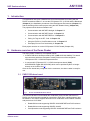
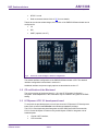
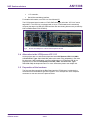
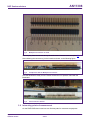
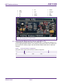
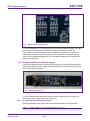
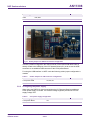
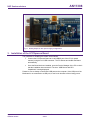
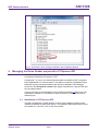
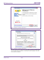
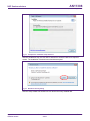
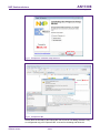
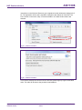
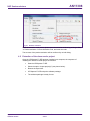
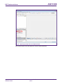
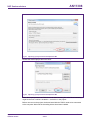
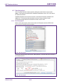
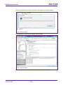
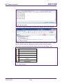
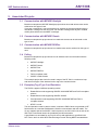
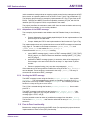
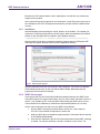
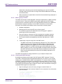
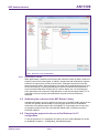
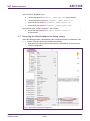
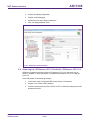
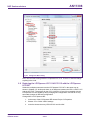
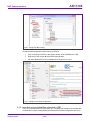
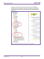
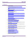
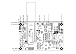
AN11308 Quick Start Up Guide PNEV512B Board Rev. 1.3 — 13 June 2013 255013 Application note COMPANY PUBLIC Document information Info Content Keywords PNEV512B, PN512, LPCXpresso, MCU, Code Red, eclipse, LPC1115, LPC1227, reader library Abstract This application note is related to the installation procedures of the PNEV512B Board. It describes the actions to be done to become acquainted with the demo reader AN11308 NXP Semiconductors PNEV512B Quick Startup Guide Revision history Rev Date Description 1.3 20130613 Added description about the P2P Snep Client 1.2 20130221 Added description of the P2P project. Added information about the use of the projects in conjunction with the LPC1227 MCU. Added information about the documentation of the NXP Reader Library. Added information about the exemplary project of code size optimization of the NXP Reader Library. 1.1 20130108 Red circles of some figures corrected 1.0 20121217 First release Contact information For more information, please visit: http://www.nxp.com For sales office addresses, please send an email to: [email protected] AN11308 Application note COMPANY PUBLIC All information provided in this document is subject to legal disclaimers. Rev. 1.3 — 13 June 2013 255013 © NXP B.V. 2013. All rights reserved. 2 of 40 AN11308 NXP Semiconductors PNEV512B Quick Startup Guide 1. Introduction This application note gives a detailed overview of the hardware for working with the PN512 contactless reader IC, we use the LPCXpresso LPC 1115/303 and the Blueboard (Chapter 2), the installation procedures of the Development Environment (Chapter 4.1) and the handling of the reader projects using the NXP Reader Library (Chapter 4.2). The projects used in this documentation are: • Communication with MIFARE Ultralight Chapter 5.1 • Communication with MIFARE Classic Chapter 5.2 • Communication with MIFARE DESFire Chapter 5.3 • Polling for Tags in the RF - field Chapter 5.4 • Using the PN512 in Card Emulation mode Chapter 5.5 • Exemplary Peer to Peer functionality Chapter 5.6 Each project can also run on the LPCXpresso LPC1227 board (Chapter 6.9). 2. Hardware overview of the Demo Reader The demo reader is made up of 2 separate boards: • A PNEV512B demo board provided by NXP (12NC: 9352 981 99699). This board has connectors which are designed to exactly fit the ones of the companion LPCXpresso LPC 1115/303 development board. • A commercial LPCXpresso LPC 1115/303 development board (12NC: 935297664598, Type: OM13035+598) which can be provided by NXP or bought directly on the market. See [1]. Once the two boards are put together via the connectors, the demo reader is ready for use. 2.1 PNEV512B demo board Fig 1. Picture of PNEV512B demo board The PNEV512B demo board embeds the contactless communication transceiver IC PN512 with all its elements needed for transmission: EMC filter, matching network and the antenna. The PN512 supports different kind of contactless communication methods and protocols at 13.56 MHz: AN11308 Application note COMPANY PUBLIC • Reader/Writer mode supporting ISO/IEC 14443A/MIFARE and FeliCa scheme • Reader/Writer mode supporting ISO/IEC 14443B • Card Operation mode supporting ISO/IEC 14443A/MIFARE and FeliCa scheme All information provided in this document is subject to legal disclaimers. Rev. 1.3 — 13 June 2013 255013 © NXP B.V. 2013. All rights reserved. 3 of 40 AN11308 NXP Semiconductors PNEV512B Quick Startup Guide • NFCIP-1 mode • Refer to the data sheets of this IC [2] for more details Thanks to the relevant solder bridges, the host link of the PNEV512B demo board can be configured for: • I²C • SPI • UART (optional, see 2.7) Fig 2. Picture of solder bridges in default configuration The default interface configuration of the PNEV512B demo board is SPI. The detailed interface configuration is described in section 2.6. Additional interface and power supply options are described in section 2.7. 2.2 CE certification of the Blueboard The current version of the demo board (v.1.4) is not CE (European Conformity) compliant. Small adaptations in the schematics may be needed to fully pass RTTE/EMC testing. 2.3 LPCXpresso LPC1115 development board To work with the provided projects, one will also need an LPCXpresso LPC development board. Such a board is not included in the Blueboard hardware package. The LPC1115 development board integrates an NXP ARM Cortex-M0 microcontroller LPC1115 with 64 Kbytes of Flash memory and 8 Kbytes of RAM. It integrates a lot of hardware parts: AN11308 Application note COMPANY PUBLIC • 1 Serial UART interface, • 1 SPI controller, All information provided in this document is subject to legal disclaimers. Rev. 1.3 — 13 June 2013 255013 © NXP B.V. 2013. All rights reserved. 4 of 40 AN11308 NXP Semiconductors PNEV512B Quick Startup Guide • 1 I²C controller, • Serial Wire test/debug interface, For detailed information, see LPC11xx User Manual [3]. The LPCXpresso board contains a JTAG/ SWD debugger called the “LPC-Link” and a target MCU. The LPC-Link is equipped with a 10-pin JTAG header and it seamlessly connects the target via USB (the USB interface and other debug features are provided by NXP’s ARM9 based LPC3154 MCU). Fig 3. Picture of LPCXpresso LPC1115 development board 2.4 Alternative to the LPCXpresso LPC1115 All the projects also run with the development board LPCXpresso LPC1114 (12NC: 935290886598, Type: OM11049+598) without the need of any adaptation in the code. By doing two subtle modification in project configuration in LPCXpresso IDE all the projects can run with the LPCXpresso LPC1227 (12NC: 935294603598, Type: OM13008+598) development board. For more information please see chapter 6.9. 2.5 Preparation of the hardware The first step after unpacking the Blue Board and the LPCXpresso is soldering the connectors onto the boards to get them together. In our example we use a multipoint connector as one can see on the pictures below. AN11308 Application note COMPANY PUBLIC All information provided in this document is subject to legal disclaimers. Rev. 1.3 — 13 June 2013 255013 © NXP B.V. 2013. All rights reserved. 5 of 40 AN11308 NXP Semiconductors PNEV512B Quick Startup Guide Fig 4. Multipoint Connectors we used One may buy these connectors at any electronic store. Here are some examples [4]. After soldering the connectors, join the boards as shown on the following figure. Fig 5. LPCXpresso with the Multipoint Connectors Now the hardware is ready for use. Please connect the LPCXpresso board with the Blueboard. Fig 6. Connect the two boards 2.6 Interesting points of measurement On the PNEV512B demo board one can find test pads for measurement purposes. AN11308 Application note COMPANY PUBLIC All information provided in this document is subject to legal disclaimers. Rev. 1.3 — 13 June 2013 255013 © NXP B.V. 2013. All rights reserved. 6 of 40 AN11308 NXP Semiconductors PNEV512B Quick Startup Guide • VCC • D7 • SIGIN • GND • ALE • SIGOUT • D5 • AUX1 • IRQ • D6 • AUX2 • VMID Fig 7. Interesting points of measurement 2.7 Preparing the Blueboard for the use with SPI or I2C The Blueboard is generally delivered in SPI configuration. To change the interface to I²C the four appropriate 0R0 resistors in the interface config section need to be resoldered to the I²C side of the solder jumpers. Also the two 0R0 resistors at A0 and A1 need to be changed. Table 1. A0 and A1 interface configuration Appropriate solder jumpers (0R0 resistors) for interface configuration Signal Interface type AN11308 Application note COMPANY PUBLIC SPI I²C UART(optional) A0 R28 R29 R29 A1 R32 R31 R32 All information provided in this document is subject to legal disclaimers. Rev. 1.3 — 13 June 2013 255013 © NXP B.V. 2013. All rights reserved. 7 of 40 AN11308 NXP Semiconductors PNEV512B Quick Startup Guide Fig 8. Blueboard in SPI configuration To use the Blueboard in I²C configuration with the provided software projects, one has to carry out two minor adaptations in the code, which are described in section 6.6. The I²C-address can be configured either by software or by hardware. To set the I²Caddress by hardware the solder jumpers in the I²C config section (see picture above) have to be connected appropriately. R7, R15 and R24 are logically LOW and R8, R16 and R22 logically HIGH. 2.8 Optional interfaces and power supply The PNEV512B demo board is normally controlled by the LPCXpresso Board. With the optional interfaces and power supply the demo board can be controlled directly by a PC without the LPCXpresso Board. Fig 9. Additional interfaces To use the additional interfaces the interface selection signals A0 and A1 have to be configured to UART mode (see section 2.6 table 1). 2.8.1 Configuring the additional interfaces With the appropriate solder jumpers two different serial interfaces can be selected. Table 2. Solder Jumpers for selecting the additional interfaces Interface type Resistors AN11308 Application note COMPANY PUBLIC All information provided in this document is subject to legal disclaimers. Rev. 1.3 — 13 June 2013 255013 © NXP B.V. 2013. All rights reserved. 8 of 40 AN11308 NXP Semiconductors PNEV512B Quick Startup Guide Interface type Resistors USB R38, R39 RS232 R40, R41, R42 Fig 10. Solder jumpers for additional interface configuration In delivery default configuration the USB-connector of the PNEV512B demo board is directly routed to the USB-pins of the LPCXpresso Board µC in order to use the USB connector as an additional USB connector of the LPCXpresso Board. For using the USB interface in UART mode the following solder jumper configuration is needed: Table 3. Solder Jumpers for USB connector configuration Connection type Resistors LPCXpresso-USB R4, R5, R6 UART-USB R12, R13, R14 2.8.2 Configuring the power supply When using the PNEV512 demo board without the LPCXpresso Board an additional 5VDC power supply is needed. The onboard voltage regulator provides the 3.3VDC supply voltage VCC. Table 4. VCC power supply configuration Power supply Resistors AN11308 Application note COMPANY PUBLIC LPCXpresso Board R3 External 5VDC R11 All information provided in this document is subject to legal disclaimers. Rev. 1.3 — 13 June 2013 255013 © NXP B.V. 2013. All rights reserved. 9 of 40 AN11308 NXP Semiconductors PNEV512B Quick Startup Guide Fig 11. Solder jumper for VCC power supply configuration 3. Installation of the LPCXpresso Board The guidelines for installing the reader are as follows: • Connect the LPCXpresso Board to a real USB2.0 port of the PC (for speed reasons) using the mini-USB connector. The PC detects and installs the Board automatically. • Once the Board has been installed, open the Device Manager of the PC to check that the installation was successful. The item “USB Device with DFU Capabilities” is being displayed. Please be sure to always connect both USB ports to the computer. If the USB port of the Blueboard is not connected to a USB port, it won’t work because of the missing power. AN11308 Application note COMPANY PUBLIC All information provided in this document is subject to legal disclaimers. Rev. 1.3 — 13 June 2013 255013 © NXP B.V. 2013. All rights reserved. 10 of 40 AN11308 NXP Semiconductors PNEV512B Quick Startup Guide Fig 12. Enumeration of the LPCXpresso Board in Device Manager Window 4. Managing the Demo Reader project with LPCXpresso IDE The demo reader project is delivered in a zip package. It can be extracted, edited, compiled and linked with LPCXpresso™ IDE. LPCXpresso™ is a new, low-cost development platform available at NXP. It supports NXP's ARM-based LPC microcontrollers. The platform comprises a simplified Eclipsebased IDE and low-cost target boards which include an attached JTAG debugger. At least use the LPCXpresso version 5.0 or higher to benefit from a bug-free IDE and the up-to-date features. This tool can freely be downloaded from the LPCXpresso website [1]. Before one can download the software, it is necessary to create an account. Creating an account is absolutely free. 4.1 Installation of LPCXpresso IDE The IDE is installed into a single directory of one’s choice. Multiple versions can be installed simultaneously without any issues. The installation starts after double-clicking the installer file. Then click “next” on the setup wizard. AN11308 Application note COMPANY PUBLIC All information provided in this document is subject to legal disclaimers. Rev. 1.3 — 13 June 2013 255013 © NXP B.V. 2013. All rights reserved. 11 of 40 AN11308 NXP Semiconductors PNEV512B Quick Startup Guide Fig 13. LPCXpresso installation setup wizard 1 Read the license agreement, then click next. Fig 14. LPCXpresso installation setup wizard 2 There are numbers of other screens on the setup wizard but generally the default options can be accepted. After the installation, an information file will be displayed. Click “Next” to accomplish the installation. AN11308 Application note COMPANY PUBLIC All information provided in this document is subject to legal disclaimers. Rev. 1.3 — 13 June 2013 255013 © NXP B.V. 2013. All rights reserved. 12 of 40 AN11308 NXP Semiconductors PNEV512B Quick Startup Guide Fig 15. LPCXpresso installation setup wizard 3 After this installation step, the user will be asked if he wants to install some required drivers. The installation of these drivers should be accepted. Fig 16. Windows Security dialog After the setup wizard has finished one can launch the newly installed IDE. AN11308 Application note COMPANY PUBLIC All information provided in this document is subject to legal disclaimers. Rev. 1.3 — 13 June 2013 255013 © NXP B.V. 2013. All rights reserved. 13 of 40 AN11308 NXP Semiconductors PNEV512B Quick Startup Guide Fig 17. LPCXpresso installation setup wizard 4 Fig 18. LPCXpresso IDE Directly after the first start of the Eclipse IDE one will see an info dialog, that this is only an unregistered copy of LPCXpresso IDE. Just confirm the dialog and follow the AN11308 Application note COMPANY PUBLIC All information provided in this document is subject to legal disclaimers. Rev. 1.3 — 13 June 2013 255013 © NXP B.V. 2013. All rights reserved. 14 of 40 AN11308 NXP Semiconductors PNEV512B Quick Startup Guide instructions on the Welcome Screen to get a registered version without the debug limit of 8k. The registration is free and is needed to navigate to the website of Code Red. The Link is shown in the menu, Help Product activation Create Serial number and Activate... Fig 19. Product activation Fig 20. Product activation If one doesn’t already have an account at Code Red, please sign up to get an activation code. The code will be sent to the provided e-mail address. AN11308 Application note COMPANY PUBLIC All information provided in this document is subject to legal disclaimers. Rev. 1.3 — 13 June 2013 255013 © NXP B.V. 2013. All rights reserved. 15 of 40 AN11308 NXP Semiconductors PNEV512B Quick Startup Guide Fig 21. Product activation Once the activation code arrives, please open the activation window by pointing to Help Product activation Enter Activation code, and enter the code. The success of the product activation will be confirmed by an info dialog. 4.2 Extraction of the demo reader project Once the LPCXpresso™ IDE has been installed on a computer, the sequence of installing the reference reader project is indicated: AN11308 Application note COMPANY PUBLIC • Start the LPCXpresso™ IDE. • Select the option “Import project(s)” (see picture below). • Browse the zip archive. • LPCXpresso™ IDE unzips the software package. • The software package is ready for use. All information provided in this document is subject to legal disclaimers. Rev. 1.3 — 13 June 2013 255013 © NXP B.V. 2013. All rights reserved. 16 of 40 AN11308 NXP Semiconductors PNEV512B Quick Startup Guide Fig 22. Importing a project into the LPCXpresso IDE At the Quick Panel on the left hand side, choose “Import projects(s)”. AN11308 Application note COMPANY PUBLIC All information provided in this document is subject to legal disclaimers. Rev. 1.3 — 13 June 2013 255013 © NXP B.V. 2013. All rights reserved. 17 of 40 AN11308 NXP Semiconductors PNEV512B Quick Startup Guide Fig 23. Importing a project into the LPCXpresso IDE Browse the desired project and click “Next”. Fig 24. Importing a project into the LPCXpresso IDE When the import process has finished one can start browsing the code. Most interesting might be the main.c which is located in ../src/main.c in the project. Before one can run the project, the demo board with the PN512 needs to be connected to the computer. Wait until the according drivers have been installed. AN11308 Application note COMPANY PUBLIC All information provided in this document is subject to legal disclaimers. Rev. 1.3 — 13 June 2013 255013 © NXP B.V. 2013. All rights reserved. 18 of 40 AN11308 NXP Semiconductors PNEV512B Quick Startup Guide 4.3 Start the project One can quickly start the reader project by editing the main function in the module main.c. This function first performs the hardware initializations of the LPC1115 and the RF transceiver PN512. Detailed descriptions of the code in the form of comments have been provided in the main.c file. This should provide a detailed overview of how to initialize certain components and get data out of and onto the card in the RF field. 4.3.1 Run the project Before running the project, please ensure that the LPCXpresso with the PNEV512B demo board is connected to the computer. Fig 25. Run the project Choose the desired project and click the Debug Button on the left hand side as shown in the example picture. Fig 26. Run the project AN11308 Application note COMPANY PUBLIC All information provided in this document is subject to legal disclaimers. Rev. 1.3 — 13 June 2013 255013 © NXP B.V. 2013. All rights reserved. 19 of 40 AN11308 NXP Semiconductors PNEV512B Quick Startup Guide After the build process one can see the size of the image in the console window. Fig 27. Run the project The initialization of the LPC-Link can take a few seconds. Fig 28. Run the project After the software upload, the execution of the project starts immediately. AN11308 Application note COMPANY PUBLIC All information provided in this document is subject to legal disclaimers. Rev. 1.3 — 13 June 2013 255013 © NXP B.V. 2013. All rights reserved. 20 of 40 AN11308 NXP Semiconductors PNEV512B Quick Startup Guide Fig 29. Run the project In the console window at the bottom one will see the debug output of the execution. Fig 30. Stop the project After the execution has reached the end of the main function please click the Terminate button to stop the execution. Otherwise one won’t be able to rerun the project. One can now do the following with the buttons near the top of the “Debug” view: Run the program. Step over C/C++ line. Step into a function. Stop the debugger. Pause execution of the running program. Instruction stepping mode (disassembly). Fig 31. Debug Buttons AN11308 Application note COMPANY PUBLIC All information provided in this document is subject to legal disclaimers. Rev. 1.3 — 13 June 2013 255013 © NXP B.V. 2013. All rights reserved. 21 of 40 AN11308 NXP Semiconductors PNEV512B Quick Startup Guide 5. Associated Projects 5.1 Communication with MIFARE Ultralight Based on examples the MIFARE Ultralight project shows how read-write access can be achieved on this type of card. If one use a card which is not write protected or secured the example program writes a valid NDEF message into the card. One can read this message with any NFC enabled mobile phone which can read NDEF messages. 5.2 Communication with MIFARE Classic Based on examples this project shows how read-write access can be achieved on this type of card. 5.3 Communication with MIFARE DESFire Based on examples this project shows how read access can be achieved on this type of card. 5.4 Polling Based on examples this project shows how to initiate a basic communication with the following cards: • MIFARE Ultralight • MIFARE Classic • MIFARE Plus • MIFARE DESFire • FeliCa compliant cards • ISO/IEC 14443-B cards This example project also looks for cards in range of the RF field in a continuous loop and returns the type of the detected card or tag to the console window. 5.5 Exemplary Tag 4 Type Card Emulation The PN512 supports 4 different operating modes: • Reader/Writer mode supporting ISO/IEC 14443A/MIFARE and FeliCa compliant scheme • Reader/Writer mode supporting ISO/IEC 14443B • Card Operation mode supporting ISO/IEC 14443A/MIFARE and FeliCa compliant scheme • NFCIP-1 mode The card operation mode is passive mode, in which the PN512 does not generate an RF field but acts as a card that modulates the field for communication with the reader. The IC only supports part of the ISO/IEC 14443-A protocol, the ISO 14443-4 A as well as the ISO 7816-4 commands need to be provided by the Microcontroller. A specification to store data for any kind of service and application is specified in the NFC Forum and it is called NFC Data Exchange Format. Storing NDEF formatted data AN11308 Application note COMPANY PUBLIC All information provided in this document is subject to legal disclaimers. Rev. 1.3 — 13 June 2013 255013 © NXP B.V. 2013. All rights reserved. 22 of 40 AN11308 NXP Semiconductors PNEV512B Quick Startup Guide inside contactless card products as mapping models as well as the management of NFC forum device as a specific platform such as a NFC Forum Type 4 Tag are defined in [7]. The following project shows an exemplary implementation of a Tag 4 Type Card on the PN512. Therefore one NDEF File and one capability container (CC) file, with ISO file identifier (ISO FID) equal to E103h, are presented to the reader. The project just offers the methods to read a URL from the card emulation and can only be seen as one example, as it is not fully validated. 5.5.1 Adaptation of the NDEF message The exemplary implementation was added to the NXP Reader Library in the following way: • Protocol Abstraction Layer: Added phpalI14443p4C for the implementation of the protocol layer for the card folder. • Comps: Added phceT4T for the implementation of the functions for Type 4 Tag. The implementation does only implement short record of NDEF messages as described in [8], page 15. The table is connected to structures *pNDEF_SHORT_text and *pNDEF_SHORT_uri in the header file ndef_message.h. A second structure is NDEF_messages, including: • type of NDEF message (type), it can be a TEXT message (NDEF_TYPE_TEXT); see [9], page 4, or a Uniform Resource Identifiers message (NDEF_TYP_URI); see [10], page 5 • parameter of NDEF message (param), it can be the index of the language for text message or the start of the URI such as ‘http://’ or ‘http://www’ or phone number. • Pointer to ‘payload’ string (*str), see also next paragraph n_mess[]. If the characters of the string shall be modified, the string in the file ndef_message.c can be adapted. These strings are connected to the array n_mess[]. This array is connected to the structure NDEF_messages. 5.5.2 Sending the NDEF message The NDEF message is sent using the function phceT4T_Listen(…) from module phceT4T.c. The main parameters are pointer to Capability Container file (CC) cet4t and pointer to the body of NDEF message ndefTagData. It is necessary to call this function in a loop as long as no error occurs. The CC file is created through the function phceT4T_SetCCFile(…) from module phceT4T.c. The NDEF message is either filled by the function Ndef_Prepare_Uri(…), if the message type is URI; see [10]; or by the function Ndef_Prepare_Text(…), if the message type is TEXT; see [9]. It is also possible to send an index of predefined messages from the table n_mess[]. The function Ndef_Decide(…) shall then be called with an array of NDEF_messages structures. 5.6 Peer to Peer functionality Based on the example performing the SNEP client (Put request) this project shows an implementation of Peer to Peer (P2P) functionality. AN11308 Application note COMPANY PUBLIC All information provided in this document is subject to legal disclaimers. Rev. 1.3 — 13 June 2013 255013 © NXP B.V. 2013. All rights reserved. 23 of 40 AN11308 NXP Semiconductors PNEV512B Quick Startup Guide Because the P2P implementation is still in alpha phase, one will find very rudimentary support for the protocol. At the moment the project supports the communication via the SPI protocol and runs on the LPCXpresso LPC1227 development board which provides sufficient 128kB of flash memory. 5.6.1 Installation After downloading and unpacking the zip file, please run the installer. The installer just copies the LPCXpresso project files to the file system. After the installation has finished, please run the included batch file located in the installation directory …\NxpRdLibP2PExtensions-x.x.x\NxpRdLib_P2PExtensions\ex\Pn512_Lpc12xx_P2P_Demo After the batch file has been executed successfully, please start the LPCXpresso IDE and import the project. Browse to the root of the installation directory. Fig 32. Importing the project After the import there are two new projects in the workspace - one for the use with the RC663 Blueboard and one for the use with the PN512 Board. Basically these two projects provide the same functionality. 5.6.2 SNEP client project In this project the LPC1227 with PNEV512B board attached behaves like SNEP client with performing the Put request functionality only [14]. On the other side there must be a device – peer capable of NFC communication and providing the SNEP server service. These conditions are fulfilled by a mobile device with Android platform (4.0 or later). Here is a short instruction list how to use the SNEP client software: 1. Run the SNEP client project as described in section 4.3.1 with respect to LPC1227 microcontroller configuration in section 6.9. 2. Hold your NFC device (smartphone) approximately 5 centimeters above antenna of the PNEV512B Blueboard. 3. Once the NFC detected in the RF field of the transmission of the NDEF message is started. You may be notified by a sound or vibration of your device. The AN11308 Application note COMPANY PUBLIC All information provided in this document is subject to legal disclaimers. Rev. 1.3 — 13 June 2013 255013 © NXP B.V. 2013. All rights reserved. 24 of 40 AN11308 NXP Semiconductors PNEV512B Quick Startup Guide transmission may take several seconds depending on the size of the NDEF message. Hold your NFC device in range of the PNEV512B board’s field during entire transmission. 4. After transmission completed there should be the transmitted image displayed in the device’s screen. 5.6.2.1 What is going on inside? The SNEP client sends a hardcoded NDEF message encapsulated in a SNEP message to the NFC device. Thanks to the SNEP client project implements the P2P Reader Library Extension compliance with the LLCP and ISO18092 protocols on the PNEV512Board’s side are ensured, implicitly a correct SNEP client-server communication. Execution of the SNEP client software can be summarized in following steps: 1. Hardware initialization 2. Detecting the RF field for an NFC peer of the tag type F. The software checks the RF field whether there is tag type F capable of performing the P2P communication 3. Once such device is found, the LLC link is activated in compliance with the procedure defined by the NFC forumError! Reference source not found.. 4. LLCP socket creation and establishing connection with other peer – SNEP server. 5. Transmission of a given image file to the SNEP server: The SNEP client sends an initial fragment 128 bytes long. Then it waits for a response from the server. Because in SNEP header it is declared longer SNEP message than one fragment, the server should response with the Continue response. The SNEP client can go on with sending the rest of the SNEP message. As soon as the entire SNEP message has been transmitted, the SNEP client shall receive the SNEP Success response from the mobile device and the transmitted picture should be immediately displayed on the mobile’s screen. The SNEP client software is deeply described in [13] in chapter 4 Sample code. 5.6.2.2 Choosing the NDEF message By default the software sends image of the NXP logo as NDEF message. There are more NDEF messages prepared in dedicated header files (see Table 5). Only a single header can be compiled with the SNEP client application. To choose another content of the NDEF message for transmission just follow the instructions below. In case of URI or text message just skip from step 1 to step 4 (steps 2 and 3 are for selection of an image). Concurrently with instructions there are parts of source code to demonstrate choosing of hardcoded PNG image file for transmission. 1. Open for editing the source file ndef_message.c located in folder src/. 2. Uncomment the line with content a header file to be transmitted. Let all the other lines commented. /* select the required type of transported data */ //#include <c_tabletxt.h> #include <c_tablepng.h> //#include <c_tablepng_NXP_QR.h> //#include <c_tablejpg_NXP_logo.h> AN11308 Application note COMPANY PUBLIC All information provided in this document is subject to legal disclaimers. Rev. 1.3 — 13 June 2013 255013 © NXP B.V. 2013. All rights reserved. 25 of 40 AN11308 NXP Semiconductors PNEV512B Quick Startup Guide 3. In Table 5 in the same row as the chosen file look up two identifiers corresponding to the chosen file. 4. In the array nmess[] uncomment the line with the couple of identifiers corresponding to the type of the chosen file. Comment all the other lines. 5. Save the changes and recompile the project. NDEF_messages n_mess[]={ /* type, parameter, string */ // {NDEF_TYPE_IMAGE,NDEF_IMAGE_JPEG,c_table, sizeof(c_table)}, {NDEF_TYPE_IMAGE,NDEF_IMAGE_PNG,c_table, sizeof(c_table)}, // {NDEF_TYPE_IMAGE,NDEF_IMAGE_TIFF,c_table, sizeof(c_table)}, // {'T', LANG_NO, text1, sizeof(text1)}, // {'T', LANG_EN, c_table, sizeof(c_table)}, // {'T', LANG_EN, text1, sizeof(text1)}, Table 5. Table of files prepared for NDEF message transmission Identifiers from the last two columns are necessary for choosing the right line from n_mess[]. NDEF message File type Content Header Name identifier identifier PNG image c_tablepng.h NDEF_TYPE_IMAGE NDEF_IMAGE_PNG QR code of NXP c_tableQR.h NDEF_TYPE_IMAGE NDEF_IMAGE_PNG Image of NXP logo c_tablenxp.h NDEF_TYPE_IMAGE NDEF_IMAGE_JPEG Long text message c_tabletxt.t ‘T’ LANG_EN 6. Supplementary Notes 6.1 Software architecture The software of the reference reader is based on the NXP reader library [5]. It intends to be simple, modular, easily readable and quickly portable by all the customers. This philosophy is reflected in its architecture which is divided into 4 layers: AN11308 Application note COMPANY PUBLIC • BAL (Bus Abstraction Layer), • HAL (Hardware Abstraction Layer) • PAL (Protocol Abstraction Layer) • AL (Abstraction Layer) All information provided in this document is subject to legal disclaimers. Rev. 1.3 — 13 June 2013 255013 © NXP B.V. 2013. All rights reserved. 26 of 40 AN11308 NXP Semiconductors PNEV512B Quick Startup Guide Fig 33. Architecture of the NXP reader library For a detailed description of the NXP Reader Library please refer to the user manual UM10663 - Quick Start Up Guide PNEV512B Board. It can be downloaded web site of the PNEV512B demo board [12]. Although it refers on examples to the CLRC663 reader IC, it still covers the NXP Reader Library for all other supported reader ICs. 6.1.1 Bus abstraction layer This layer offers functions to abstract the hardware parts of the LPC11XX microcontroller. These functions use the specific libraries available for the LPC11XX family microcontroller. Based on these stacks, the communication routines for the relevant physical media I2C/SPI can be easily designed. These drivers are specific for the LPC11XX family and therefore cannot be ported to other microcontrollers. 6.1.2 Hardware abstraction layer This layer offers functions to abstract the hardware parts of the transceiver PN512. 6.1.3 Protocol abstraction layer Every PAL function is a low level function realizing a single functionality. It is encapsulated in a module which is independent from the others. The user can easily design his application by doing a drag-and-drop of the relevant module. The following PAL modules are available in this software package: AN11308 Application note COMPANY PUBLIC • ISO/IEC 14443-3A, • ISO/IEC 14443-3B, • ISO/IEC 14443-4A/B, • MIFARE, • ISO/IEC15693, • FeliCa, All information provided in this document is subject to legal disclaimers. Rev. 1.3 — 13 June 2013 255013 © NXP B.V. 2013. All rights reserved. 27 of 40 AN11308 NXP Semiconductors PNEV512B Quick Startup Guide • NFC Initiator 6.1.4 Application layer Lying on the previous software layers, the application layer is on top of the reader software package. It combines elements of the previous three parts into high level functionalities. 6.2 Build configuration All the projects mentioned in Chapter 5 are available in the debug configuration. Additionally, the Polling and SNEP client project comprises the release configuration. • Debug configuration This configuration is mainly used when the target board is attached to the PC with the JTAG debugger. It allows the display of debug messages in the console window, which is useful in the early stage of the project. • Release configuration Once the project is debugged and mature, it might be interesting to use the release configuration, to use the hardware stand alone. No debug messages are displayed in the console window. Note, that only in Release Configuration one can flash the software onto the Blueboard and start it automatically, once power has been attached to the board. The build configuration can be selected as follows: • Click on the project PN512 in the project window of the LPCXpresso™ IDE, • Right click of the mouse Select Build Configuration, • Set active Debug1227 build (or Release1227 build) for LPC 1115. Fig 34. Select the build configuration AN11308 Application note COMPANY PUBLIC All information provided in this document is subject to legal disclaimers. Rev. 1.3 — 13 June 2013 255013 © NXP B.V. 2013. All rights reserved. 28 of 40 AN11308 NXP Semiconductors PNEV512B Quick Startup Guide 6.3 Setting MCU There are many LPC microcontrollers supported by the LPCXpresso IDE build in compiler. Before compiling a project, the correct MCU need to be set. • Right click the project choose properties (at the bottom) • C/C++ build MCU settings expand LPC11xx MCU group click LPC1115/303 click OK Fig 35. Selection of MCU 6.4 Level of compiler optimization When the code size at the current compiler level overloads the FLASH size of the target board (64K for the ARM-based microcontroller LPC 1115), a higher compiler optimization level can be selected to reduce the code size of the project. The following steps can be followed to select a level of compiler optimization: AN11308 Application note COMPANY PUBLIC • Click on the project PN512 in the project window of the LPCXpresso™ IDE, • Right click of the mouse Select properties Select C/C++ build, • Select Settings Optimization, • Choose the desired level in the combo box. All information provided in this document is subject to legal disclaimers. Rev. 1.3 — 13 June 2013 255013 © NXP B.V. 2013. All rights reserved. 29 of 40 AN11308 NXP Semiconductors PNEV512B Quick Startup Guide Fig 36. Select the level of optimization 6.4.1 Optimization issues When optimization is enabled, it will reorder code. What this means is that the code from multiple C lines will be intermingled. In addition, assignments and initializations might be pulled out of loops so they are only executed once. Changes like these will make the code confusing to debug. Some symptoms one might see are breakpoints that only work the first time through, or seeing the debugger’s current line indicator fail to advance or even move backwards when clicking step. It is best to always use –O0 for debugging. Since optimization can make such a big difference in code size and performance, it is a good idea to test one’s project with optimization and plan for a final build that is optimized. 6.5 Optimizing the code size of the NXP Reader Library A detailed description on how to optimize the code size of the NXP Reader Library for the use with one specially defined reader IC and card type please refer to the attached documents on the product page of the CLEV663B [11]. On that page one can also find an exemplary project for the use of the MIFARE Classic card in conjunction with the CLRC663 reader IC. 6.6 Preparing the projects for the use of the Blueboard in I²C configuration To use the projects in I²C configuration one has to do some small adaptations in the file ph_NxpBuild.h located in .. src\NxpRdLib_PublicRelease\types. AN11308 Application note COMPANY PUBLIC All information provided in this document is subject to legal disclaimers. Rev. 1.3 — 13 June 2013 255013 © NXP B.V. 2013. All rights reserved. 30 of 40 AN11308 NXP Semiconductors PNEV512B Quick Startup Guide Open the file ph_NxpBuild.h and a. ensure that #define NXPBUILD__PHBAL_REG_STUB uncommented b. uncomment the line #define NXPBUILD__PHHAL_HW_BUS_I2C. c. comment the line #define NXPBUILD__PHHAL_HW_BUS_SPI. d. comment the line #define NXPBUILD__PHHAL_HW_BUS_UART. Open the file driver_config.h located in ..\lpc1115 and a. ensure that the line #define CONFIG_ENABLE_DRIVER_I2C uncommented 1 6.7 Removing the initial breakpoint on debug startup When the debugger starts, it automatically sets a breakpoint at the first statement in the main() function. One can remove this breakpoint as follows: 1. Right click on the project and choose Launch Configurations Open Current Launch Configuration. Fig 37. Open Current Launch Configuration AN11308 Application note COMPANY PUBLIC All information provided in this document is subject to legal disclaimers. Rev. 1.3 — 13 June 2013 255013 © NXP B.V. 2013. All rights reserved. 31 of 40 AN11308 NXP Semiconductors PNEV512B Quick Startup Guide 2. Choose the Debug configuration 3. Choose the tab Debugger 4. Uncheck the box near “Stop on startup at:” 5. Click onto Apply and then Close. Fig 38. Disable the initial breakpoint 6.8 Replacing the LPCXpresso LPC1115 with the LPCXpresso LPC1114 Solder the multipoint connector onto the LPCXpresso LPC1114 in the same way as shown in Chapter 0. At this point there is no difference between the LPC1114 and the LPC1115. In the IDE please do the following changes: 1. In the menu of the LPCXpresso IDE choose Project Properties. 2. Choose C/C++ Build MCU settings. 3. In the list choose the entry LPC1114/301 or LPC1114/302 according to the used board and click OK. AN11308 Application note COMPANY PUBLIC All information provided in this document is subject to legal disclaimers. Rev. 1.3 — 13 June 2013 255013 © NXP B.V. 2013. All rights reserved. 32 of 40 AN11308 NXP Semiconductors PNEV512B Quick Startup Guide Fig 39. Change the MCU setting Now, one can start working with the LPCXpresso LPC1114. There is no need to change anything in the code. 6.9 Replacing the LPCXpresso LPC1114/LPC1115 with the LPCXpresso LPC1227 Solder the multipoint connector onto the LPCXpresso LPC1227 in the same way as shown in Chapter 2.5. At this point there is no difference between the LPC1114/LPC1115 and the LPC1227. The projects for the LPC1114/LPC1115 are fully compatible with the LPCXpresso LPC1227 board by easily changing IDE configuration. One has to do only two subtle changes in IDE build configuration. Change MCU in LPCXpresso IDE 1. In the menu of the LPCXpresso IDE choose Project Properties. 2. Choose C/C++ Build MCU settings. 3. In the list choose the entry LPC1227/301 and click OK. AN11308 Application note COMPANY PUBLIC All information provided in this document is subject to legal disclaimers. Rev. 1.3 — 13 June 2013 255013 © NXP B.V. 2013. All rights reserved. 33 of 40 AN11308 NXP Semiconductors PNEV512B Quick Startup Guide Fig 40. Change the MCU setting Set either Build Configuration either Debug or Release • Click on the project PN512 in the project window of the LPCXpresso™ IDE, • Right click of the mouse Select Build Configuration, • Set active Debug1227 build (or Release1227 build) for LPC 1227. Fig 41. Change Active Build configuration 6.10 Included and excluded files mismatch in IDE There is a misunderstood in LPCXpresso v4.2.3 regarding to displaying of included and excluded files. Despite setting Debug1227/Release1227 Build Configuration active, on AN11308 Application note COMPANY PUBLIC All information provided in this document is subject to legal disclaimers. Rev. 1.3 — 13 June 2013 255013 © NXP B.V. 2013. All rights reserved. 34 of 40 AN11308 NXP Semiconductors PNEV512B Quick Startup Guide project pane in the lpc1227 directory there are scource and linker files displayed strikethrough like the were not used in compilation. One might be confused whether correct files are used for compilation – Build Configuration. Just follow the instructions from the Chapter 6.9 which ensures correct source files shall be compiled and linker scripts used. Fig 42. Included and excluded fiels are mismatched in the project pane AN11308 Application note COMPANY PUBLIC All information provided in this document is subject to legal disclaimers. Rev. 1.3 — 13 June 2013 255013 © NXP B.V. 2013. All rights reserved. 35 of 40 AN11308 NXP Semiconductors PNEV512B Quick Startup Guide 7. References [1] LPCXpresso website www.nxp.com/redirect/lpcxpresso.code-red-tech.com/LPCXpresso [2] PN512 product information and data sheet http://www.nxp.com/products/interface_and_connectivity/nfc_devices/series/PN512 .html [3] LPC11XX family User Manual www.nxp.com/redirect/ics.nxp.com/support/documents/microcontrollers/pdf/ lpcxpresso.getting.started [4] Multipoint Connectors we used: Grid Dimension: 2.54mm, at least 27 pins www.nxp.com/redirect/bklelectronic.de/index.php/catalog/product/view/id/9644/s/10120182/category/72/ and www.nxp.com/redirect/bklelectronic.de/index.php/catalog/product/view/id/9688/s/10120802/category/73/ or www.nxp.com/redirect/conrad.at/ce/de/product/741119/STIFTLEISTE-1-X-36POLIG-VERGOL-RM-254 and www.nxp.com/redirect/conrad.at/ce/de/product/736427/BUCHSENLEISTEEINREIHIG-36-POLIG-RM254 [5] Direct link to the NXP Reader Library http://www.nxp.com/documents/software/200310.zip [6] Using the PNEV512B in Card Emulation mode http://www.nxp.com/demoboard/PNEV512B.html [7] TYPE 4 TAG: NFC Forum, Type 4 Tag Operation Specification, Version 1.0, March 13, 2007 www.nxp.com/redirect/nfc-forum.org/specs [8] NDEF: NFC Data Exchange Format (NDEF), Technical Specification, NFC Forum, Revision 1.0, July 24, 2006 www.nxp.com/redirect/nfc-forum.org/specs [9] TEXT RTD: Text Record Type Definition, Technical Specification, NFC Forum, RTD-Text 1.0, July 24, 2006 www.nxp.com/redirect/nfc-forum.org/specs [10] URI RTD: URI Record Type Definition, Technical Specification, NFC Forum, RTD-URI 1.0, July 24, 2006 www.nxp.com/redirect/nfc-forum.org/specs [11] CLEV663B demo board site http://www.nxp.com/demoboard/CLEV663B.html [12] PNEV512B demo board site http://www.nxp.com/demoboard/PNEV512B.html [13] NXP Reader Library P2P user manual UM10721_NXP_Reader_Library_P2P AN11308 Application note COMPANY PUBLIC All information provided in this document is subject to legal disclaimers. Rev. 1.3 — 13 June 2013 255013 © NXP B.V. 2013. All rights reserved. 36 of 40 AN11308 NXP Semiconductors PNEV512B Quick Startup Guide [14] Technical Specification – Simple NDEF Exchange Protocol, NFCForum-TSSNEP_1.0, available on www.nxp.com/redirect/nfc-forum.org/specs/spec_license [15] Technical Specification Logical Link Control Protocol, NFCForum-TS-LLCP_1.1, available on www.nxp.com/redirect/nfc-forum.org/specs/spec_license AN11308 Application note COMPANY PUBLIC All information provided in this document is subject to legal disclaimers. Rev. 1.3 — 13 June 2013 255013 © NXP B.V. 2013. All rights reserved. 37 of 40 AN11308 NXP Semiconductors PNEV512B Quick Startup Guide 8. Legal information 8.1 Definitions Draft — The document is a draft version only. The content is still under internal review and subject to formal approval, which may result in modifications or additions. NXP Semiconductors does not give any representations or warranties as to the accuracy or completeness of information included herein and shall have no liability for the consequences of use of such information. 8.2 Disclaimers Limited warranty and liability — Information in this document is believed to be accurate and reliable. However, NXP Semiconductors does not give any representations or warranties, expressed or implied, as to the accuracy or completeness of such information and shall have no liability for the consequences of use of such information. In no event shall NXP Semiconductors be liable for any indirect, incidental, punitive, special or consequential damages (including - without limitation lost profits, lost savings, business interruption, costs related to the removal or replacement of any products or rework charges) whether or not such damages are based on tort (including negligence), warranty, breach of contract or any other legal theory. Notwithstanding any damages that customer might incur for any reason whatsoever, NXP Semiconductors’ aggregate and cumulative liability towards customer for the products described herein shall be limited in accordance with the Terms and conditions of commercial sale of NXP Semiconductors. Right to make changes — NXP Semiconductors reserves the right to make changes to information published in this document, including without limitation specifications and product descriptions, at any time and without notice. This document supersedes and replaces all information supplied prior to the publication hereof. Suitability for use — NXP Semiconductors products are not designed, authorized or warranted to be suitable for use in life support, life-critical or safety-critical systems or equipment, nor in applications where failure or malfunction of an NXP Semiconductors product can reasonably be expected to result in personal injury, death or severe property or environmental damage. NXP Semiconductors accepts no liability for inclusion and/or use of NXP Semiconductors products in such equipment or applications and therefore such inclusion and/or use is at the customer’s own risk. Applications — Applications that are described herein for any of these products are for illustrative purposes only. NXP Semiconductors makes no representation or warranty that such applications will be suitable for the specified use without further testing or modification. Customers are responsible for the design and operation of their applications and products using NXP Semiconductors products, and NXP Semiconductors accepts no liability for any assistance with applications or customer product design. It is customer’s sole responsibility to determine whether the NXP Semiconductors product is suitable and fit for the customer’s applications and products planned, as well as for the planned application and use of customer’s third party customer(s). Customers should provide appropriate design and operating safeguards to minimize the risks associated with their applications and products. testing for the customer’s applications and products using NXP Semiconductors products in order to avoid a default of the applications and the products or of the application or use by customer’s third party customer(s). NXP does not accept any liability in this respect. Export control — This document as well as the item(s) described herein may be subject to export control regulations. Export might require a prior authorization from competent authorities. Evaluation products — This product is provided on an “as is” and “with all faults” basis for evaluation purposes only. NXP Semiconductors, its affiliates and their suppliers expressly disclaim all warranties, whether express, implied or statutory, including but not limited to the implied warranties of noninfringement, merchantability and fitness for a particular purpose. The entire risk as to the quality, or arising out of the use or performance, of this product remains with customer. In no event shall NXP Semiconductors, its affiliates or their suppliers be liable to customer for any special, indirect, consequential, punitive or incidental damages (including without limitation damages for loss of business, business interruption, loss of use, loss of data or information, and the like) arising out the use of or inability to use the product, whether or not based on tort (including negligence), strict liability, breach of contract, breach of warranty or any other theory, even if advised of the possibility of such damages. Notwithstanding any damages that customer might incur for any reason whatsoever (including without limitation, all damages referenced above and all direct or general damages), the entire liability of NXP Semiconductors, its affiliates and their suppliers and customer’s exclusive remedy for all of the foregoing shall be limited to actual damages incurred by customer based on reasonable reliance up to the greater of the amount actually paid by customer for the product or five dollars (US$5.00). The foregoing limitations, exclusions and disclaimers shall apply to the maximum extent permitted by applicable law, even if any remedy fails of its essential purpose. 8.3 Licenses Purchase of NXP ICs with ISO/IEC 14443 type B functionality This NXP Semiconductors IC is ISO/IEC 14443 Type B software enabled and is licensed under Innovatron’s Contactless Card patents license for ISO/IEC 14443 B. The license includes the right to use the IC in systems and/or end-user equipment. RATP/Innovatron Technology 8.4 Trademarks Notice: All referenced brands, product names, service names and trademarks are property of their respective owners. MIFARE — is a trademark of NXP B.V. DESFire — is a trademark of NXP B.V. MIFARE Ultralight — is a trademark of NXP B.V. MIFARE Plus — is a trademark of NXP B.V. NXP Semiconductors does not accept any liability related to any default, damage, costs or problem which is based on any weakness or default in the customer’s applications or products, or the application or use by customer’s third party customer(s). Customer is responsible for doing all necessary AN11308 Application note COMPANY PUBLIC All information provided in this document is subject to legal disclaimers. Rev. 1.3 — 13 June 2013 255013 © NXP B.V. 2013. All rights reserved. 38 of 40 AN11308 NXP Semiconductors PNEV512B Quick Startup Guide 9. List of figures Fig 1. Fig 2. Fig 3. Fig 4. Fig 5. Fig 6. Fig 7. Fig 8. Fig 9. Fig 10. Fig 11. Fig 12. Fig 13. Fig 14. Fig 15. Fig 16. Fig 17. Fig 18. Fig 19. Fig 20. Picture of PNEV512B demo board.................... 3 Picture of solder bridges in default configuration ..................................................... 4 Picture of LPCXpresso LPC1115 development board ................................................................. 5 Multipoint Connectors we used ......................... 6 LPCXpresso with the Multipoint Connectors ..... 6 Connect the two boards .................................... 6 Interesting points of measurement .................... 7 Blueboard in SPI configuration.......................... 8 Additional interfaces .......................................... 8 Solder jumpers for additional interface configuration ..................................................... 9 Solder jumper for VCC power supply configuration ................................................... 10 Enumeration of the LPCXpresso Board in Device Manager Window ................................ 11 LPCXpresso installation setup wizard 1 .......... 12 LPCXpresso installation setup wizard 2 .......... 12 LPCXpresso installation setup wizard 3 .......... 13 Windows Security dialog ................................. 13 LPCXpresso installation setup wizard 4 .......... 14 LPCXpresso IDE ............................................. 14 Product activation ........................................... 15 Product activation ........................................... 15 AN11308 Application note COMPANY PUBLIC Fig 21. Fig 22. Fig 23. Fig 24. Fig 25. Fig 26. Fig 27. Fig 28. Fig 29. Fig 30. Fig 31. Fig 32. Fig 33. Fig 34. Fig 35. Fig 36. Fig 37. Fig 38. Fig 39. Fig 40. Fig 41. Fig 42. Product activation ............................................16 Importing a project into the LPCXpresso IDE ..17 Importing a project into the LPCXpresso IDE ..18 Importing a project into the LPCXpresso IDE ..18 Run the project ................................................19 Run the project ................................................19 Run the project ................................................20 Run the project ................................................20 Run the project ................................................21 Stop the project ...............................................21 Debug Buttons ................................................21 Importing the project .......................................24 Architecture of the NXP reader library .............27 Select the build configuration ..........................28 Selection of MCU ............................................29 Select the level of optimization ........................30 Open Current Launch Configuration ...............31 Disable the initial breakpoint ...........................32 Change the MCU setting .................................33 Change the MCU setting .................................34 Change Active Build configuration ..................34 Included and excluded fiels are mismatched in the project pane ..............................................35 All information provided in this document is subject to legal disclaimers. Rev. 1.3 — 13 June 2013 255013 © NXP B.V. 2013. All rights reserved. 39 of 40 AN11308 NXP Semiconductors PNEV512B Quick Startup Guide 10. Contents 1. 2. 2.1 2.2 2.3 2.4 2.5 2.6 2.7 Introduction ......................................................... 3 Hardware overview of the Demo Reader ........... 3 PNEV512B demo board ..................................... 3 CE certification of the Blueboard ........................ 4 LPCXpresso LPC1115 development board ....... 4 Alternative to the LPCXpresso LPC1115 ........... 5 Preparation of the hardware ............................... 5 Interesting points of measurement ..................... 6 Preparing the Blueboard for the use with SPI or 2 I C ...................................................................... 7 2.8 Optional interfaces and power supply ................ 8 2.8.1 Configuring the additional interfaces .................. 8 2.8.2 Configuring the power supply ............................. 9 3. Installation of the LPCXpresso Board ............. 10 4. Managing the Demo Reader project with LPCXpresso IDE ................................................ 11 4.1 Installation of LPCXpresso IDE ........................ 11 4.2 Extraction of the demo reader project .............. 16 4.3 Start the project ................................................ 19 4.3.1 Run the project ................................................. 19 5. Associated Projects .......................................... 22 5.1 Communication with MIFARE Ultralight ........... 22 5.2 Communication with MIFARE Classic .............. 22 5.3 Communication with MIFARE DESFire ............ 22 5.4 Polling .............................................................. 22 5.5 Exemplary Tag 4 Type Card Emulation ........... 22 5.5.1 Adaptation of the NDEF message .................... 23 5.5.2 Sending the NDEF message ............................ 23 5.6 Peer to Peer functionality ................................. 23 5.6.1 Installation ........................................................ 24 5.6.2 SNEP client project .......................................... 24 5.6.2.1 What is going on inside? .................................. 25 5.6.2.2 Choosing the NDEF message .......................... 25 6. Supplementary Notes ....................................... 26 6.1 Software architecture ....................................... 26 6.1.1 Bus abstraction layer........................................ 27 6.1.2 Hardware abstraction layer .............................. 27 6.1.3 Protocol abstraction layer ................................. 27 6.1.4 Application layer ............................................... 28 6.2 Build configuration............................................ 28 6.3 Setting MCU ..................................................... 29 6.4 Level of compiler optimization .......................... 29 6.4.1 Optimization issues .......................................... 30 6.5 Optimizing the code size of the NXP Reader Library .............................................................. 30 6.6 6.7 6.8 6.9 6.10 7. 8. 8.1 8.2 8.3 8.4 9. 10. Preparing the projects for the use of the Blueboard in I²C configuration ..........................30 Removing the initial breakpoint on debug startup ..............................................................31 Replacing the LPCXpresso LPC1115 with the LPCXpresso LPC1114 .....................................32 Replacing the LPCXpresso LPC1114/LPC1115 with the LPCXpresso LPC1227 ........................33 Included and excluded files mismatch in IDE ...34 References .........................................................36 Legal information ..............................................38 Definitions.........................................................38 Disclaimers .......................................................38 Licenses ...........................................................38 Trademarks ......................................................38 List of figures .....................................................39 Contents .............................................................40 Please be aware that important notices concerning this document and the product(s) described herein, have been included in the section 'Legal information'. © NXP B.V. 2013. All rights reserved. For more information, visit: http://www.nxp.com For sales office addresses, please send an email to: [email protected] Date of release: 13 June 2013 255013 Document identifier: AN11308