1
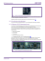
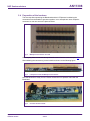
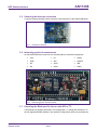
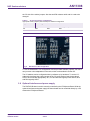
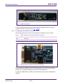
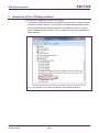
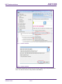
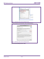
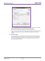
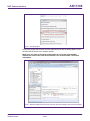
AN11308 Quick Start Up Guide PNEV512B Board Rev. 1.9 — 11 November 2015 255019 Application note COMPANY PUBLIC Document information Info Content Keywords PN512, Blueboard, LPCXpresso, MCU, Code Red, eclipse, LPC1769, LPC1227, NFC Reader Library, PNEV512B Abstract This application note is related to the installation procedures of the PNEV512B Board. It describes the actions to be done to become acquainted with the demo reader AN11308 NXP Semiconductors PNEV512B Quick Startup Guide Revision history Rev Date Description 1.9 Updated all relevant parts in respect to the NFC Reader Library update 20151111 Removed LPC1227 support 1.8 20141201 Added a note about RAM limitation of LPC1227. 1.7 20140721 Small corrections 1.6 20140519 Removed the note about the version of the LPCXpresso IDE. Some small corrections. Changed the description and pictures of the projects Polling and, Classic Changed the P2P description due to a software update. Removed the description about the projects Ultralight and DESFire. All projects are now based on the NFC Reader Library version 3.010. Therefore all projects have been refactored. Added support for the development board LPCXpresso LPC1769 which is based on an ARM Cortex M3 microcontroller. The NFC Reader Library is now called NFC Reader Library 1.5 20140114 Added description for Card Emulation T4T and T2T. 1.4 20131011 Added info about what version of the LPCXpresso IDE to use. 1.3 20130613 Added description about the P2P Snep Client 1.2 20130221 Added description of the P2P project. Added information about the use of the projects in conjunction with the LPC1227 MCU. Added information about the documentation of the NFC Reader Library. Added information about the exemplary project of code size optimization of the NFC Reader Library. 1.1 20130108 Red circles of some figures corrected 1.0 20121217 First release Contact information For more information, please visit: http://www.nxp.com For sales office addresses, please send an email to: [email protected] AN11308 Application note COMPANY PUBLIC All information provided in this document is subject to legal disclaimers. Rev. 1.9 — 11 November 2015 255019 © NXP Semiconductors N.V. 2015. All rights reserved. 2 of 36 AN11308 NXP Semiconductors PNEV512B Quick Startup Guide 1. Introduction This application note gives a detailed overview of the hardware for working with the PN512 contactless reader IC, we use the LPCXpresso LPC 1769 and the Blueboard (Chapter 2), the installation procedures of the Development Environment (Chapter 4.1) and the handling of the reader projects using the NFC Reader Library (Chapter 0). The projects used and explained in this documentation are: Table 1. Example projects Example projects delivered with the NFC Reader Library Example Description Example 1 – Basic Discovery Loop Explains how to poll for different technologies (Tag, P2P, HCE), detect and report them. Default configuration parameters are used. Example 2 – Explains how to poll for different technologies (Tag, P2P, HCE), detect and Advanced Discovery report them. All configuration parameters are used and explained. Loop AN11308 Application note COMPANY PUBLIC Example 3 – NFC Forum Explains how to configure the NFC Reader Library for different P2P modes such as Active Mode, Target Mode, Initiator Mode and SNEP Client/Server. Example 4 – MIFARE Classic Explains the usage of standard MIFARE commands. Example 8 – HCE T4T Explains how to emulate a NFC Forum Type 4 Tag supporting read and write operations. Example 9 – NTAGI2C Explains NTAG-I2C specific commands. All information provided in this document is subject to legal disclaimers. Rev. 1.9 — 11 November 2015 255019 © NXP Semiconductors N.V. 2015. All rights reserved. 3 of 36 AN11308 NXP Semiconductors PNEV512B Quick Startup Guide 2. Hardware overview of the Demo Reader The demo reader is made up of 2 separate boards: • A PNEV512B demo board provided by NXP (12NC: 9352 981 99699). This board has connectors which are designed to exactly fit the ones of the companion LPCXpresso LPC 1769 development boards. • A commercial LPCXpresso LPC 1769 development board (12NC: 935291912598, Type: OM13000+598) which can be provided by NXP or bought directly on the market. See Ref. [11]. Once the two boards are put together via the connectors, the demo reader is ready for use. 2.1 PNEV512B demo board Fig 1. Picture of PNEV512B demo board The PNEV512B demo board embeds the contactless communication transceiver IC PN512 with all its elements needed for transmission: EMC filter, matching network and the antenna. The PN512 supports different kind of contactless communication methods and protocols at 13.56 MHz: • Reader/Writer mode supporting ISO/IEC 14443A/MIFARE and FeliCa scheme • Reader/Writer mode supporting ISO/IEC 14443B • Card Operation mode supporting ISO/IEC 14443A/MIFARE and FeliCa scheme • NFCIP-1 mode • Refer to the data sheet of this IC [2] for more details Thanks to the relevant solder bridges, the host link of the PNEV512B demo board can be configured for: • I²C • SPI • UART (optional, see Section 2.7) AN11308 Application note COMPANY PUBLIC All information provided in this document is subject to legal disclaimers. Rev. 1.9 — 11 November 2015 255019 © NXP Semiconductors N.V. 2015. All rights reserved. 4 of 36 AN11308 NXP Semiconductors PNEV512B Quick Startup Guide Fig 2. Picture of solder bridges in default configuration The default interface configuration of the PNEV512B demo board is SPI. The detailed interface configuration is described in section 2.7. Additional interface and power supply options are described in section 2.8. 2.2 CE certification of the Blueboard The current version of the demo board (v.1.5) is CE (European Conformity) compliant. 2.3 LPCXpresso LPC1769 development board To work with the provided projects, one will also need an LPCXpresso LPC development board. Such a board is not included in the Blueboard hardware package. The LPC1769 development board integrates an NXP ARM Cortex-M3 microcontroller LPC1769 with 512 Kbytes of Flash memory and 64 Kbytes of RAM. It integrates a lot of hardware parts: • Serial UART interface, • SPI controller, • I2C controller, • Serial Wire test/debug interface, • For detailed information, see LPC1769 product site [3] The LPCXpresso board contains a JTAG/ SWD debugger called the “LPC-Link” and a target MCU. LPC-Link is equipped with a 10-pin JTAG header and it seamlessly connects to the target via USB (the USB interface and other debug features are provided by NXP’s ARM9 based LPC3154 MCU). Fig 3. AN11308 Application note COMPANY PUBLIC Picture of LPCXpresso LPC1769 development board All information provided in this document is subject to legal disclaimers. Rev. 1.9 — 11 November 2015 255019 © NXP Semiconductors N.V. 2015. All rights reserved. 5 of 36 AN11308 NXP Semiconductors PNEV512B Quick Startup Guide 2.4 Preparation of the hardware The first step after unpacking the Blueboard and the LPCXpresso is soldering the connectors onto the boards to get them together. In our example we use a multipoint connector as one can see on the pictures below. Fig 4. Multipoint Connectors we used One may buy these connectors at any electronic store. Here are some examples [4]. After soldering the connectors, join the boards as shown on the following figure. Fig 5. LPCXpresso with the Multipoint Connectors Now the hardware is ready for use. Please connect the LPCXpresso board with the Blueboard. Fig 6. AN11308 Application note COMPANY PUBLIC Connect the two boards All information provided in this document is subject to legal disclaimers. Rev. 1.9 — 11 November 2015 255019 © NXP Semiconductors N.V. 2015. All rights reserved. 6 of 36 AN11308 NXP Semiconductors PNEV512B Quick Startup Guide 2.5 Soldering the interrupt connection To get the interrupt working, please connect the pins 26 and 27 of the PNEV512B board. Fig 7. Interrupt connection 2.6 Interesting points of measurement On the PNEV512B demo board one can find test pads for measurement purposes. • VCC • D7 • SIGIN • GND • ALE • SIGOUT • D5 • AUX1 • IRQ • D6 • AUX2 • VMID Fig 8. Interesting points of measurement 2.7 Preparing the Blueboard for the use with SPI or I2C The Blueboard is generally delivered in SPI configuration. To change the interface to I²C the four appropriate 0R0 resistors in the interface config section need to be resoldered to AN11308 Application note COMPANY PUBLIC All information provided in this document is subject to legal disclaimers. Rev. 1.9 — 11 November 2015 255019 © NXP Semiconductors N.V. 2015. All rights reserved. 7 of 36 AN11308 NXP Semiconductors PNEV512B Quick Startup Guide the I²C side of the solder jumpers. Also the two 0R0 resistors at A0 and A1 need to be changed. Table 2. A0 and A1 interface configuration Appropriate solder jumpers (0R0 resistors) for interface configuration Signal Interface type SPI I²C UART(optional) A0 R28 R29 R29 A1 R32 R31 R32 Fig 9. Blueboard in SPI configuration To use the Blueboard in I²C configuration with the provided software projects, one has to carry out two minor adaptations in the code, which are described in section 6.5. The I²C-address can be configured either by software or by hardware. To set the I²Caddress by hardware the solder jumpers in the I²C config section (see picture above) have to be connected appropriately. R7, R15 and R24 are logically LOW and R8, R16 and R22 logically HIGH. 2.8 Optional interfaces and power supply The PNEV512B demo board is normally controlled by the LPCXpresso Board. With the optional interfaces and power supply the demo board can be controlled directly by a PC without the LPCXpresso Board. AN11308 Application note COMPANY PUBLIC All information provided in this document is subject to legal disclaimers. Rev. 1.9 — 11 November 2015 255019 © NXP Semiconductors N.V. 2015. All rights reserved. 8 of 36 AN11308 NXP Semiconductors PNEV512B Quick Startup Guide Fig 10. Additional interfaces To use the additional interfaces the interface selection signals A0 and A1 have to be configured to UART mode (see section 2.7, Table 2). 2.8.1 Configuring the additional interfaces With the appropriate solder jumpers two different serial interfaces can be selected. Table 3. Solder Jumpers for selecting the additional interfaces Interface type Resistors USB R38, R39 RS232 R40, R41, R42 Fig 11. Solder jumpers for additional interface configuration In delivery default configuration the USB-connector of the PNEV512B demo board is directly routed to the USB-pins of the LPCXpresso Board µC in order to use the USB connector as an additional USB connector of the LPCXpresso Board. For using the USB interface in UART mode the following solder jumper configuration is needed: AN11308 Application note COMPANY PUBLIC All information provided in this document is subject to legal disclaimers. Rev. 1.9 — 11 November 2015 255019 © NXP Semiconductors N.V. 2015. All rights reserved. 9 of 36 AN11308 NXP Semiconductors PNEV512B Quick Startup Guide Table 4. Solder Jumpers for USB connector configuration Connection type Resistors LPCXpresso-USB R4, R5, R6 UART-USB R12, R13, R14 2.8.2 Configuring the power supply When using the PNEV512 demo board without the LPCXpresso Board an additional 5VDC power supply is needed. The onboard voltage regulator provides the 3.3VDC supply voltage VCC. Table 5. VCC power supply configuration Power supply Resistors LPCXpresso Board R3 External 5VDC R11 Fig 12. Solder jumper for VCC power supply configuration 2.9 Other supported system architectures The projects described in this guide are also available on Linux. The projects are preconfigured for the use on the Raspberry Pi with the Raspbian image. The SPI interface is used for the communication between the application and the NFC controller. The software and the start guide can be downloaded at the product page of the EXPLORE-NFC [12]. Although this guide only describes the use of the EXPLORE-NFC extension board, it also supports the PNEV512B Blueboard. The Blueboard can be used with a special adaptor called BluePi. For information about how to configure the hardware and the software please refer to section 6.7. AN11308 Application note COMPANY PUBLIC All information provided in this document is subject to legal disclaimers. Rev. 1.9 — 11 November 2015 255019 © NXP Semiconductors N.V. 2015. All rights reserved. 10 of 36 AN11308 NXP Semiconductors PNEV512B Quick Startup Guide 3. Installation of the LPCXpresso Board The guidelines for installing the reader are as follows: • Connect the LPCXpresso Board to a real USB2.0 port of the PC (for speed reasons) using the mini-USB connector. The PC detects and installs the Board automatically. Once the Board has been installed, open the Device Manager of the PC to check that the installation was successful. The item “USB Device with DFU Capabilities” is being displayed. Fig 13. Enumeration of the LPCXpresso Board in Device Manager Window AN11308 Application note COMPANY PUBLIC All information provided in this document is subject to legal disclaimers. Rev. 1.9 — 11 November 2015 255019 © NXP Semiconductors N.V. 2015. All rights reserved. 11 of 36 AN11308 NXP Semiconductors PNEV512B Quick Startup Guide 4. Managing the Demo Reader project with LPCXpresso IDE The demo reader project is delivered in a zip package. It can be extracted, edited, compiled and linked with LPCXpresso IDE. LPCXpresso is a new, low-cost development platform available from NXP. It supports NXP's ARM-based LPC microcontrollers. The platform is comprised of a simplified Eclipse-based IDE and low-cost target boards which include an attached JTAG debugger. This tool can freely be downloaded from the LPCXpresso website [1]. 4.1 Installation of LPCXpresso IDE The IDE is installed into a single directory of one’s choice. Multiple versions can be installed simultaneously without side effects. The installation starts after double-clicking the installer file. Fig 14. LPCXpresso installation NXP Debug drivers Make sure, the checkboxes for installing the NXP Debug drivers are activated. During the installation, the user will be asked if he wants to install some required drivers. The installation of these drivers should be accepted. AN11308 Application note COMPANY PUBLIC All information provided in this document is subject to legal disclaimers. Rev. 1.9 — 11 November 2015 255019 © NXP Semiconductors N.V. 2015. All rights reserved. 12 of 36 AN11308 NXP Semiconductors PNEV512B Quick Startup Guide Fig 15. Windows Security dialog After the setup wizard has finished one can launch the newly installed IDE. Fig 16. LPCXpresso IDE Directly after the first start of the Eclipse IDE one will see an info dialogue that this is only an unregistered copy of LPCXpresso IDE. Just confirm the dialog and follow the instructions on the Welcome Screen to get a registered version without the debug limit of 8k. The registration is free and can be done at the LPCware website. The Link is shown in the menu, Help Activate Create Serial number and register... AN11308 Application note COMPANY PUBLIC All information provided in this document is subject to legal disclaimers. Rev. 1.9 — 11 November 2015 255019 © NXP Semiconductors N.V. 2015. All rights reserved. 13 of 36 AN11308 NXP Semiconductors PNEV512B Quick Startup Guide Fig 17. Product activation Fig 18. Product activation If one doesn’t already have an account at LPCware, please sign up to get an activation code. The code will be sent to the provided e-mail address. AN11308 Application note COMPANY PUBLIC All information provided in this document is subject to legal disclaimers. Rev. 1.9 — 11 November 2015 255019 © NXP Semiconductors N.V. 2015. All rights reserved. 14 of 36 AN11308 NXP Semiconductors PNEV512B Quick Startup Guide Fig 19. Product activation Once the activation code arrives please open the activation window by pointing to Help Activate Activate (Free Edition), and enter the code. The success of the product activation will be confirmed by an info dialogue. 4.2 Extraction of the demo reader project All demo reader projects are divided into three sub projects. One project that contains the NFC Reader Library, one project that contains the FreeRTOS operating system, one project that contains all hardware dependent parts and one project that contains the example application. All projects are distributed in one zip package that can be imported into the LPCXpresso IDE in one single action. The following example is based on this package. The sequence of installing the reference reader projects is indicated: • Start the LPCXpresso IDE. • Select the option “Import project(s)” (see picture below). • Browse the zip archive. • LPCXpresso IDE unzips the software package. • The software package is ready for use. AN11308 Application note COMPANY PUBLIC All information provided in this document is subject to legal disclaimers. Rev. 1.9 — 11 November 2015 255019 © NXP Semiconductors N.V. 2015. All rights reserved. 15 of 36 AN11308 NXP Semiconductors PNEV512B Quick Startup Guide Fig 20. Importing a project into the LPCXpresso IDE In the Quick Panel on the left hand side, choose “Import projects(s)”. Fig 21. Importing a project into the LPCXpresso IDE Browse the desired package and click “Next”. AN11308 Application note COMPANY PUBLIC All information provided in this document is subject to legal disclaimers. Rev. 1.9 — 11 November 2015 255019 © NXP Semiconductors N.V. 2015. All rights reserved. 16 of 36 AN11308 NXP Semiconductors PNEV512B Quick Startup Guide Fig 22. Importing a project into the LPCXpresso IDE For a working demo project you need to import at least four sub projects. One example project, the NFC Reader Library, FreeRTOS and one MCU project. When the import process has finished one can start browsing the code. Before one can run the project, the LPCXpresso board containing the PN512 Blueboard needs to be connected to the computer. Wait until the adequate drivers have been installed. 4.3 Run the project Before running the project, please ensure that the LPCXpresso with the Blueboard is connected to the computer. Please also make sure that the correct microcontroller and the correct build configurations are chosen. Information about how to do this can be found in the sections 6.2 and 6.3. AN11308 Application note COMPANY PUBLIC All information provided in this document is subject to legal disclaimers. Rev. 1.9 — 11 November 2015 255019 © NXP Semiconductors N.V. 2015. All rights reserved. 17 of 36 AN11308 NXP Semiconductors PNEV512B Quick Startup Guide Fig 23. Run the project Choose the project that contains the user application and click the Debug Button on the left hand side as shown in the example picture. Make sure, the name of the build configuration as well as the selected MCU matches the name of the used microcontroller. See sections and 6.3 for further information. Fig 24. After the build process one can see the size of the image in the console window. AN11308 Application note COMPANY PUBLIC All information provided in this document is subject to legal disclaimers. Rev. 1.9 — 11 November 2015 255019 © NXP Semiconductors N.V. 2015. All rights reserved. 18 of 36 AN11308 NXP Semiconductors PNEV512B Quick Startup Guide Fig 25. Run the project After the software upload, the execution of the project starts immediately, but might halt at the initial breakpoint. To resume execution, just click onto the resume button. Fig 26. Debugging controls AN11308 Application note COMPANY PUBLIC All information provided in this document is subject to legal disclaimers. Rev. 1.9 — 11 November 2015 255019 © NXP Semiconductors N.V. 2015. All rights reserved. 19 of 36 AN11308 NXP Semiconductors PNEV512B Quick Startup Guide Fig 27. Run the project In the console window at the bottom one will see the debug output of the execution. After the execution has reached the end of the main function please click the Terminate button to stop the execution. Otherwise one won’t be able to rerun the project. One can now do the following with the buttons near the top of the “Debug” view: Run the program. Step over C/C++ line. Step into a function. Stop the debugger. Pause execution of the running program. Instruction stepping mode (disassembly). Fig 28. Debug Buttons AN11308 Application note COMPANY PUBLIC All information provided in this document is subject to legal disclaimers. Rev. 1.9 — 11 November 2015 255019 © NXP Semiconductors N.V. 2015. All rights reserved. 20 of 36 AN11308 NXP Semiconductors PNEV512B Quick Startup Guide 5. Associated Projects All example projects are available for download at the product page of the PNEV512B [7] in the documents section and are being distributed in one single file. All projects are packaged into a single installer file. After downloading the zip file please extract it and run the installer. The installer just copies all you need to get started to your hard disk. 5.1 Example 1 – Basic Discovery Loop The Discovery Loop can be seen as the entry point when starting to communicate with an NFC tag or device. It scans the close environment for tags and devices of different technologies in range. In case something has been found, the Discovery Loop performs the anti-collision and identification. The obtained information are then passed back to the developer. Fig 29. Discovery Loop in Poll mode AN11308 Application note COMPANY PUBLIC All information provided in this document is subject to legal disclaimers. Rev. 1.9 — 11 November 2015 255019 © NXP Semiconductors N.V. 2015. All rights reserved. 21 of 36 AN11308 NXP Semiconductors PNEV512B Quick Startup Guide The example application first initializes the hardware, configures the host interface and continues execution in the function BasicDiscoveryLoop_Demo() in file NfcrdlibEx1_BasicDiscoveryLoop.c. This function is the core of the example. It shows the initialization of the NFC Reader Library as well as the execution of the Discovery Loop. After the Discovery Loop has been executed, the user can see how to differently handle the detected tags or devices depending on the technology. 5.2 Example 2 – Advanced Discovery Loop Additionally to Example 1 the Advanced Discovery Loop example explains the different configuration options of the Discovery Loop. 5.3 Example 3 – NFC Forum Explains how to configure the NFC Reader Library for different P2P modes such as Active Mode, Target Mode, Initiator Mode and SNEP Client/Server. In Snep Server mode the example waits for a connection from a Snep Client. In case a Snep Client transmits an NDEF message, the application displays it in the console window of the LPCXpresso IDE. In Snep Client mode, the application tries to connect to a Snep Server. Once the connection is established, it transmits an NDEF message to the server. 5.4 Example 4 – MIFARE Classic Basic read/write operations on MIFARE Classic cards are demonstrated with this example. It shows the developer the most important operations to get started with these cards. 5.5 Example 6 – EMVCo Loopback The EMVCo Loopback application is provided together with the NFC Reader Library to help the customer reaching EMVCo Level 1 certification for his device. The example itself produces no output in the console window of the LPCXpresso IDE. 5.6 Example 7 – EMVCo Polling The EMVCo Polling example demonstrates how to configure the NFC Reader Library as specified by EMVCo specification and starts polling for EMVCo cards. Once an EMVCo compatible card is found, it demonstrates the exchange of APDU commands. This example shall help the developer getting started more quickly when working with EMVCo cards. 5.7 Example 8 – HCE T4T Example 8 implements a Type 4 Tag card emulation according to NFC Forum Type 4 Tag specification. The example supports all specified commands such as Select, ReadBinary, UpdateBinary. AN11308 Application note COMPANY PUBLIC All information provided in this document is subject to legal disclaimers. Rev. 1.9 — 11 November 2015 255019 © NXP Semiconductors N.V. 2015. All rights reserved. 22 of 36 AN11308 NXP Semiconductors PNEV512B Quick Startup Guide 5.8 Example 9 – NTAG-I2C The NTAG-I2C example demonstrates the use of special features which are needed to work with the NTAG-I2C. For more details about the NTAG-I2C and its functionalities please consult the product page of the same [13]. AN11308 Application note COMPANY PUBLIC All information provided in this document is subject to legal disclaimers. Rev. 1.9 — 11 November 2015 255019 © NXP Semiconductors N.V. 2015. All rights reserved. 23 of 36 AN11308 NXP Semiconductors PNEV512B Quick Startup Guide 6. Supplementary Notes Fore detailed API description of the NFC Reader Library please refer to the chm help file located at NFC_Reader_Library\docs\14_user_doc\NXP NFC Reader Library.chm. 6.1 General Software Architecture The software of the reference reader is based on the NFC Reader Library [5]. It intends to be simple, modular, easily readable and quickly portable by all the customers. This philosophy is reflected in its architecture which is divided into 4 layers: • BAL (Bus Abstraction Layer), • HAL (Hardware Abstraction Layer) • PAL (Protocol Abstraction Layer) • AL (Abstraction Layer) Fig 30. Architecture of the NFC Reader Library For a detailed description of the NFC Reader Library please refer to the user manual UM10721 - NXP NFC Reader Library User Manual. Documentation of the API can be found in the document UM10802 - NXP NFC Reader Library API. Both can be downloaded at the web site of the PNEV512B demo board [7]. 6.1.1 Bus abstraction layer This layer offers functions to abstract the hardware parts of the microcontroller. These functions connect to the specific peripheral drivers of the microcontroller. Based on these stacks, the communication routines for the relevant physical media I2C/SPI can be easily designed. These drivers used in this examples are specific for the LPC1XXX AN11308 Application note COMPANY PUBLIC All information provided in this document is subject to legal disclaimers. Rev. 1.9 — 11 November 2015 255019 © NXP Semiconductors N.V. 2015. All rights reserved. 24 of 36 AN11308 NXP Semiconductors PNEV512B Quick Startup Guide family and therefore cannot be ported to other microcontrollers. If one want’s to change the microcontroller, he would have to adapt this layer. 6.1.2 Hardware abstraction layer This layer offers functions to abstract the hardware parts of the supported transceivers. 6.1.3 Protocol abstraction layer Every PAL function is a low level function realizing a single functionality. It is encapsulated in a module which is independent from the others. The user can easily design his application by doing a drag-and-drop of the relevant module. The following PAL modules are available in this software package: • ISO/IEC 14443-3A, • ISO/IEC 14443-3B, • ISO/IEC 14443-4, • MIFARE, • ISO/IEC 14443-4mC • FeliCa, • NFC Initiator • NFC Target • ISO/IEC 15693 • ISO/IEC 18000-3 Mode 3 6.1.4 Application layer Lying on the previous software layers, the application layer is on top of the reader software package. It combines elements of the previous three parts into high level functionalities. 6.1.5 NFC Activity This component provides the Discovery Loop component. It implements poll mode based on NFC Activity Specification 1.1 (backward compatibility with version 1.0) and EMVCo Specification 2.3.1a. Listen mode is implemented based on NFC Activity Specification 1.1. Support for Type V (ISO 15693) polling is included based on NFC Forum draft specification. ISO 18000-3 Mode 3 (EPC Gen2) is supported as a proprietary technology in poll mode. 6.1.6 HCE Layer This component implements the card emulation of NFC Forum Type 4A Tag. The implementation is based on NFC Forum Type 4 Tag Operation Specification version 2.0. SELECT, READ BINARY and UPDATE BINARY commands are supported as per NFC Forum Type 4 Tag Operation Specification. This layer follows a multi-threaded RTOS based design using one reader library thread and one application thread. Application thread along with application callback can be used for handling of UPDATE BINARY and proprietary commands. AN11308 Application note COMPANY PUBLIC All information provided in this document is subject to legal disclaimers. Rev. 1.9 — 11 November 2015 255019 © NXP Semiconductors N.V. 2015. All rights reserved. 25 of 36 AN11308 NXP Semiconductors PNEV512B Quick Startup Guide A pictorial representation of reader library thread and application thread used for card emulation is shown below. Refer function documentation for more information. Fig 31. State machine diagram of the T4T HCE example application As UPDATE BINARY and proprietary commands are handled by the phceT4T_AppProcessCmd in application thread, application shall use some synchronization mechanism (like mutex or semaphore) as shown in the diagram to synchronize entry to and exit from phceT4T_Activate and phceT4T_AppProcessCmd. Waiting Time eXtension (WTX) is handled internally by phceT4T_Activate in reader library thread. The reader library thread should be of high priority than the application thread for proper handling of WTX. In non RTOS single threaded environment this layer can be used with limited features, i.e. with no support for WTX. 6.1.7 NFC Apps The example applications make use of the underlying functions. They provide entry points for the developers to get started with the NFC Reader Library more quickly. 6.2 Build configuration All the projects mentioned in this guide are available in debug and release configuration. • Debug configuration This configuration is mainly used when the target board is attached to the PC with the JTAG debugger. It allows the display of debug messages in the console window, which is useful in the early stage of the project. • Release configuration AN11308 Application note COMPANY PUBLIC All information provided in this document is subject to legal disclaimers. Rev. 1.9 — 11 November 2015 255019 © NXP Semiconductors N.V. 2015. All rights reserved. 26 of 36 AN11308 NXP Semiconductors PNEV512B Quick Startup Guide Once the project is debugged and mature, it might be interesting to use the release configuration, to use the hardware stand alone. No debug messages are displayed in the console window. Note, that only in Release Configuration one can flash the software onto the Blueboard and start it automatically, once power has been attached to the board. The build configuration can be selected as follows: • Click on the project in the project window of the LPCXpresso IDE, • Right click of the mouse Select Build Configuration, • Set active DebugLPC1769 build (or ReleaseLPC1769 build) for LPC 1769. Fig 32. Select the build configuration Note: When switching from one MCU to another, please take care to also switch to the correct MCU setting within the LPCXpresso IDE. See section 6.3. 6.3 Setting the MCU There are many LPC microcontrollers supported by the LPCXpresso IDE build in compiler. Before compiling a project, the correct MCU need to be set. • Right click the project choose properties (at the bottom) • C/C++ build MCU settings expand desired LPC1xxx MCU group choose the correct microcontroller click OK AN11308 Application note COMPANY PUBLIC All information provided in this document is subject to legal disclaimers. Rev. 1.9 — 11 November 2015 255019 © NXP Semiconductors N.V. 2015. All rights reserved. 27 of 36 AN11308 NXP Semiconductors PNEV512B Quick Startup Guide Fig 33. Selection of the LPC1769 MCU 6.4 Level of compiler optimization When the code size at the current compiler level overloads the FLASH size of the target board, a higher compiler optimization level can be selected to reduce the code size of the project. The following steps can be followed to select a level of compiler optimization: • Click on the application project in the project window of the LPCXpresso IDE, • Right click of the mouse Select properties Select C/C++ build, • Select Settings Optimization, • Choose the desired level in the combo box. AN11308 Application note COMPANY PUBLIC All information provided in this document is subject to legal disclaimers. Rev. 1.9 — 11 November 2015 255019 © NXP Semiconductors N.V. 2015. All rights reserved. 28 of 36 AN11308 NXP Semiconductors PNEV512B Quick Startup Guide Fig 34. Select the level of optimization 6.4.1 Optimization issues When optimization is enabled, it will reorder code. What this means is that the code from multiple C lines will be intermingled. In addition, assignments and initializations might be pulled out of loops so they are only executed once. Changes like these will make the code confusing to debug. Some symptoms one might see are breakpoints that only work the first time through, or seeing the debugger’s current line indicator fail to advance or even move backwards when clicking step. It is best to always use –O0 for debugging. 6.5 Preparing the projects for the use of the Blueboard in I²C configuration To use the projects in I²C configuration one has to do some small adaptations in the file phhwConfig.h located in the MCU project LPC1xxx. 1. Open the file ../LPC1769/phLpc1768_Build.h and a. Uncomment the line #define I2C_USED. b. Comment the line #define SPI_USED. 6.6 Removing the initial breakpoint on debug startup When the debugger starts, it automatically sets a breakpoint at the first statement in the main() function. One can remove this breakpoint as follows: 1. Right click on the project and choose Launch Configurations Edit current… AN11308 Application note COMPANY PUBLIC All information provided in this document is subject to legal disclaimers. Rev. 1.9 — 11 November 2015 255019 © NXP Semiconductors N.V. 2015. All rights reserved. 29 of 36 AN11308 NXP Semiconductors PNEV512B Quick Startup Guide Fig 35. Open Current Launch Configuration 1. Choose the Debug configuration 2. Choose the tab Debugger 3. Uncheck the box near “Stop on startup at:” 4. Click onto Apply and then Close. AN11308 Application note COMPANY PUBLIC All information provided in this document is subject to legal disclaimers. Rev. 1.9 — 11 November 2015 255019 © NXP Semiconductors N.V. 2015. All rights reserved. 30 of 36 AN11308 NXP Semiconductors PNEV512B Quick Startup Guide 6.7 Using the Blueboard with the Raspberry Pi Detailed instructions about how to run the NFC Reader Library on the Raspberry Pi can be found in the Start Guide linked at the product page of the EXPLORE-NFC [12]. This sub chapter only describes some information that is not included in the start guide of the EXPLORE-NFC. 6.7.1 Preparing the hardware a. Connector for the Blueboard b. Connector for the Raspberry Pi Fig 36. BluePi adaptor • Connect the PNEV512B Blueboard to the BluePi adaptor. • Connect the adaptor to the Raspberry Pi Fig 37. PNEV512B Blueboard connected to the Raspberry Pi AN11308 Application note COMPANY PUBLIC All information provided in this document is subject to legal disclaimers. Rev. 1.9 — 11 November 2015 255019 © NXP Semiconductors N.V. 2015. All rights reserved. 31 of 36 AN11308 NXP Semiconductors PNEV512B Quick Startup Guide 7. References [1] LPCXpresso website http://www.lpcware.com/lpcxpresso/download [2] PN512 product information and data sheet http://www.nxp.com/products/interface_and_connectivity/nfc_contactless_reader_ic s/series/PN512.html [3] LPC176x/5x User manual http://www.nxp.com/documents/user_manual/UM10360.pdf [4] Multipoint Connectors we used: Grid Dimension: 2.54mm, at least 27 pins http://www.conrad.at/ce/de/product/741119/STIFTLEISTE and http://www.conrad.at/ce/de/product/736427/BUCHSENLEISTE-EINREIHIG [5] Direct link to the NFC Reader Library Not yet available [6] TYPE 4 TAG: NFC Forum, Type 4 Tag Operation Specification, Version 2.0, March 13, 2007 http://www.nfc-forum.org/specs [7] PNEV512B demo board site http://www.nxp.com/demoboard/PNEV512B.html [8] NXP NFC Reader Library User Manual http://www.nxp.com/documents/user_manual/UM10721.pdf [9] Technical Specification – Simple NDEF Exchange Protocol, NFCForum-TSSNEP_1.0 http://www.nfc-forum.org/specs/spec_license [10] EMV – The table of card types and their matching AIDs are available on http://www.en.wikipedia.org/wiki/EMV [11] LPCXpresso LPC1769 development board http://www.nxp.com/demoboard/OM13000.html [12] EXPLORE-NFC product page http://www.nxp.com/demoboard/PNEV512R.html#documentation [13] NTAG-I2C http://www.nxp.com/products/identification_and_security/nfc_and_reader_ics/conne cted_tag_solutions/series/NT3H1101_NT3H1201.html AN11308 Application note COMPANY PUBLIC All information provided in this document is subject to legal disclaimers. Rev. 1.9 — 11 November 2015 255019 © NXP Semiconductors N.V. 2015. All rights reserved. 32 of 36 AN11308 NXP Semiconductors PNEV512B Quick Startup Guide 8. Legal information 8.1 Definitions Draft — The document is a draft version only. The content is still under internal review and subject to formal approval, which may result in modifications or additions. NXP Semiconductors does not give any representations or warranties as to the accuracy or completeness of information included herein and shall have no liability for the consequences of use of such information. 8.2 Disclaimers Limited warranty and liability — Information in this document is believed to be accurate and reliable. However, NXP Semiconductors does not give any representations or warranties, expressed or implied, as to the accuracy or completeness of such information and shall have no liability for the consequences of use of such information. In no event shall NXP Semiconductors be liable for any indirect, incidental, punitive, special or consequential damages (including - without limitation lost profits, lost savings, business interruption, costs related to the removal or replacement of any products or rework charges) whether or not such damages are based on tort (including negligence), warranty, breach of contract or any other legal theory. Notwithstanding any damages that customer might incur for any reason whatsoever, NXP Semiconductors’ aggregate and cumulative liability towards customer for the products described herein shall be limited in accordance with the Terms and conditions of commercial sale of NXP Semiconductors. Right to make changes — NXP Semiconductors reserves the right to make changes to information published in this document, including without limitation specifications and product descriptions, at any time and without notice. This document supersedes and replaces all information supplied prior to the publication hereof. Suitability for use — NXP Semiconductors products are not designed, authorized or warranted to be suitable for use in life support, life-critical or safety-critical systems or equipment, nor in applications where failure or malfunction of an NXP Semiconductors product can reasonably be expected to result in personal injury, death or severe property or environmental damage. NXP Semiconductors accepts no liability for inclusion and/or use of NXP Semiconductors products in such equipment or applications and therefore such inclusion and/or use is at the customer’s own risk. Applications — Applications that are described herein for any of these products are for illustrative purposes only. NXP Semiconductors makes no representation or warranty that such applications will be suitable for the specified use without further testing or modification. Customers are responsible for the design and operation of their applications and products using NXP Semiconductors products, and NXP Semiconductors accepts no liability for any assistance with applications or customer product design. It is customer’s sole responsibility to determine whether the NXP Semiconductors product is suitable and fit for the customer’s applications and products planned, as well as for the planned application and use of customer’s third party customer(s). Customers should provide appropriate design and operating safeguards to minimize the risks associated with their applications and products. NXP Semiconductors does not accept any liability related to any default, damage, costs or problem which is based on any weakness or default in the customer’s applications or products, or the application or use by customer’s AN11308 Application note COMPANY PUBLIC third party customer(s). Customer is responsible for doing all necessary testing for the customer’s applications and products using NXP Semiconductors products in order to avoid a default of the applications and the products or of the application or use by customer’s third party customer(s). NXP does not accept any liability in this respect. Export control — This document as well as the item(s) described herein may be subject to export control regulations. Export might require a prior authorization from competent authorities. Evaluation products — This product is provided on an “as is” and “with all faults” basis for evaluation purposes only. NXP Semiconductors, its affiliates and their suppliers expressly disclaim all warranties, whether express, implied or statutory, including but not limited to the implied warranties of noninfringement, merchantability and fitness for a particular purpose. The entire risk as to the quality, or arising out of the use or performance, of this product remains with customer. In no event shall NXP Semiconductors, its affiliates or their suppliers be liable to customer for any special, indirect, consequential, punitive or incidental damages (including without limitation damages for loss of business, business interruption, loss of use, loss of data or information, and the like) arising out the use of or inability to use the product, whether or not based on tort (including negligence), strict liability, breach of contract, breach of warranty or any other theory, even if advised of the possibility of such damages. Notwithstanding any damages that customer might incur for any reason whatsoever (including without limitation, all damages referenced above and all direct or general damages), the entire liability of NXP Semiconductors, its affiliates and their suppliers and customer’s exclusive remedy for all of the foregoing shall be limited to actual damages incurred by customer based on reasonable reliance up to the greater of the amount actually paid by customer for the product or five dollars (US$5.00). The foregoing limitations, exclusions and disclaimers shall apply to the maximum extent permitted by applicable law, even if any remedy fails of its essential purpose. 8.3 Licenses Purchase of NXP ICs with ISO/IEC 14443 type B functionality This NXP Semiconductors IC is ISO/IEC 14443 Type B software enabled and is licensed under Innovatron’s Contactless Card patents license for ISO/IEC 14443 B. The license includes the right to use the IC in systems and/or end-user equipment. RATP/Innovatron Technology 8.4 Trademarks Notice: All referenced brands, product names, service names and trademarks are property of their respective owners. MIFARE — is a trademark of NXP Semiconductors N.V. DESFire — is a trademark of NXP Semiconductors N.V. MIFARE Ultralight — is a trademark of NXP Semiconductors N.V. MIFARE Plus — is a trademark of NXP Semiconductors N.V. All information provided in this document is subject to legal disclaimers. Rev. 1.9 — 11 November 2015 255019 © NXP Semiconductors N.V. 2015. All rights reserved. 33 of 36 AN11308 NXP Semiconductors PNEV512B Quick Startup Guide 9. List of tables Table 1. Table 2. Table 3. Example projects .............................................. 3 A0 and A1 interface configuration ..................... 8 Solder Jumpers for selecting the additional interfaces .......................................................... 9 AN11308 Application note COMPANY PUBLIC Table 4. Table 5. Solder Jumpers for USB connector configuration....................................................10 VCC power supply configuration .....................10 All information provided in this document is subject to legal disclaimers. Rev. 1.9 — 11 November 2015 255019 © NXP B.V. 2015. All rights reserved. 34 of 36 AN11308 NXP Semiconductors PNEV512B Quick Startup Guide 10. List of figures Fig 1. Fig 2. Fig 3. Fig 4. Fig 5. Fig 6. Fig 7. Fig 8. Fig 9. Fig 10. Fig 11. Fig 12. Fig 13. Fig 14. Fig 15. Fig 16. Fig 17. Fig 18. Picture of PNEV512B demo board.................... 4 Picture of solder bridges in default configuration ..................................................... 5 Picture of LPCXpresso LPC1769 development board ................................................................. 5 Multipoint Connectors we used ......................... 6 LPCXpresso with the Multipoint Connectors ..... 6 Connect the two boards .................................... 6 Interrupt connection .......................................... 7 Interesting points of measurement .................... 7 Blueboard in SPI configuration.......................... 8 Additional interfaces .......................................... 9 Solder jumpers for additional interface configuration ..................................................... 9 Solder jumper for VCC power supply configuration ................................................... 10 Enumeration of the LPCXpresso Board in Device Manager Window ................................ 11 LPCXpresso installation NXP Debug drivers .. 12 Windows Security dialog ................................. 13 LPCXpresso IDE ............................................. 13 Product activation ........................................... 14 Product activation ........................................... 14 AN11308 Application note COMPANY PUBLIC Fig 19. Fig 20. Fig 21. Fig 22. Fig 23. Fig 24. Fig 25. Fig 26. Fig 27. Fig 28. Fig 29. Fig 30. Fig 31. Fig 32. Fig 33. Fig 34. Fig 35. Fig 36. Fig 37. Product activation ............................................15 Importing a project into the LPCXpresso IDE ..16 Importing a project into the LPCXpresso IDE ..16 Importing a project into the LPCXpresso IDE ..17 Run the project ................................................18 After the build process one can see the size of the image in the console window. ...................18 Run the project ................................................19 Debugging controls .........................................19 Run the project ................................................20 Debug Buttons ................................................20 Discovery Loop in Poll mode ...........................21 Architecture of the NFC Reader Library ..........24 State machine diagram of the T4T HCE example application ........................................26 Select the build configuration ..........................27 Selection of the LPC1769 MCU ......................28 Select the level of optimization ........................29 Open Current Launch Configuration ...............30 BluePi adaptor.................................................31 PNEV512B Blueboard connected to the Raspberry Pi ...................................................31 All information provided in this document is subject to legal disclaimers. Rev. 1.9 — 11 November 2015 255019 © NXP Semiconductors N.V. 2015. All rights reserved. 35 of 36 AN11308 NXP Semiconductors PNEV512B Quick Startup Guide 11. Contents 1. 2. 2.1 2.2 2.3 2.4 2.5 2.6 2.7 2.8 2.8.1 2.8.2 2.9 3. 4. 4.1 4.2 4.3 5. 5.1 5.2 5.3 5.4 5.5 5.6 5.7 5.8 6. 6.1 6.1.1 6.1.2 6.1.3 6.1.4 Introduction ......................................................... 3 Hardware overview of the Demo Reader ........... 4 PNEV512B demo board ..................................... 4 CE certification of the Blueboard ........................ 5 LPCXpresso LPC1769 development board ....... 5 Preparation of the hardware ............................... 6 Soldering the interrupt connection...................... 7 Interesting points of measurement ..................... 7 Preparing the Blueboard for the use with SPI or I2C ...................................................................... 7 Optional interfaces and power supply ................ 8 Configuring the additional interfaces .................. 9 Configuring the power supply ........................... 10 Other supported system architectures ............. 10 Installation of the LPCXpresso Board ............. 11 Managing the Demo Reader project with LPCXpresso IDE ................................................ 12 Installation of LPCXpresso IDE ........................ 12 Extraction of the demo reader project .............. 15 Run the project ................................................. 17 Associated Projects .......................................... 21 Example 1 – Basic Discovery Loop .................. 21 Example 2 – Advanced Discovery Loop ........... 22 Example 3 – NFC Forum.................................. 22 Example 4 – MIFARE Classic .......................... 22 Example 6 – EMVCo Loopback ....................... 22 Example 7 – EMVCo Polling ............................ 22 Example 8 – HCE T4T ..................................... 22 Example 9 – NTAG-I2C ................................... 23 Supplementary Notes ....................................... 24 General Software Architecture ......................... 24 Bus abstraction layer........................................ 24 Hardware abstraction layer .............................. 25 Protocol abstraction layer ................................. 25 Application layer ............................................... 25 6.1.5 6.1.6 6.1.7 6.2 6.3 6.4 6.4.1 6.5 6.6 6.7 6.7.1 7. 8. 8.1 8.2 8.3 8.4 9. 10. NFC Activity......................................................25 HCE Layer ........................................................25 NFC Apps .........................................................26 Build configuration ............................................26 Setting the MCU ...............................................27 Level of compiler optimization ..........................28 Optimization issues ..........................................29 Preparing the projects for the use of the Blueboard in I²C configuration ..........................29 Removing the initial breakpoint on debug startup ..............................................................29 Using the Blueboard with the Raspberry Pi ......31 Preparing the hardware ....................................31 References .........................................................32 Legal information ..............................................33 Definitions.........................................................33 Disclaimers .......................................................33 Licenses ...........................................................33 Trademarks ......................................................33 List of figures .....................................................35 Contents .............................................................36 Please be aware that important notices concerning this document and the product(s) described herein, have been included in the section 'Legal information'. © NXP Semiconductors N.V. 2015. All rights reserved. For more information, visit: http://www.nxp.com For sales office addresses, please send an email to: [email protected] Date of release: 11 November 2015 255019 Document identifier: AN11308