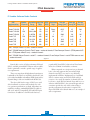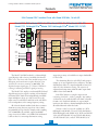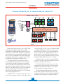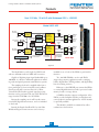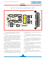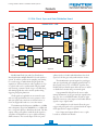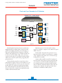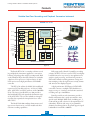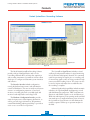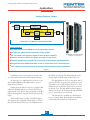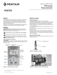
1
® Putting FPGAs to Work in Software Radio Systems Fifth Edition Technology FPGA Resources Products Applications Links by Rodger H. Hosking Vice President & Cofounder of Pentek, Inc. Pentek, Inc. One Park Way, Upper Saddle River, New Jersey 07458 Tel: (201) 818 5900 • Fax: (201) 818 5904 Email: [email protected] • http://www.pentek.com Copyright © 2005, 2007, 2008, 2009, 2010 Pentek Inc. Last Updated: May 2010 All rights reserved. Contents of this publication may not be reproduced in any form without written permission. Specifications are subject to change without notice. Pentek, GateFlow, ReadyFow, SystemFlow and RTS are registered trademarks of Pentek, Inc. 1 Pentek, Inc. • One Park Way, Upper Saddle River, NJ 07458 • Tel: (201) 818-5900 • Fax: (201) 818-5904 • Email: [email protected] • http://www.pentek.com Putting FPGAs to Work in Software Radio Systems Preface FPGAs have become an increasingly important resource for software radio systems. Programmable logic technology now offers significant advantages for implementing software radio functions such as DDCs (Digital Downconverters). Over the past few years, the functions associated with DDCs have seen a shift from being delivered in ASICs (Application-Specific ICs) to operating as IP (Intellectual Property) in FPGAs. For many applications, this implementation shift brings advantages that include design flexibility, higher precision processing, higher channel density, lower power, and lower cost per channel. With the advent of each new, higher-performance FPGA family, these benefits continue to increase. This handbook introduces the basics of FPGA technology and its relationship to SDR (Software Defined Radio) systems. A review of Pentek’s GateFlow FPGA Design Resources is followed by a discussion of features and benefits of FPGA-based DDCs. Pentek SDR products that utilize FPGA technology and applications based on such products are also presented. For a more in-depth discussion of SDR systems, the reader is referred to Pentek’s Software Defined Radio Handbook, now in its 7th Edition. 2 Pentek, Inc. • One Park Way, Upper Saddle River, NJ 07458 • Tel: (201) 818-5900 • Fax: (201) 818-5904 • Email: [email protected] • http://www.pentek.com Putting FPGAs to Work in Software Radio Systems Technology Typical Software Radio System DDC Digital Downconverter Analog RF Signal RF TUNER Analog IF Signal A/D CONV Digital IF Samples DIGITAL MIXER LOWPASS FILTER Software Radio Tasks Digital Baseband Samples DSP DIGITAL LOCAL OSC Figure 1 Figure 2 Here we’ve ranked some of the popular signal processing tasks associated with SDR systems on a two axis graph, with compute Processing Intensity on the vertical axis and Flexibility on the horizontal axis. We begin our discussion with the basic elements of a software radio receiver system. The front end usually contains an analog RF amplifier and often an analog RF translator. This translates the high frequency RF signals down to a frequency that an A/D converter can handle. This is usually below 200 MHz and is often an IF output. What we mean by process intensity is the degree of highly-repetitive and rather primitive operations. At the upper left are dedicated functions like A/D converters and DDCs that require specialized hardware structures to complete the operations in real time. ASICs are usually chosen for these functions. The A/D output feeds the DDC (Digital Downconverter) stage, which is typically contained in a monolithic chip which forms the heart of a software radio system. Flexibility pertains to the uniqueness or variability of the processing and how likely the function may have to be changed or customized for any specific application. At the lower right are tasks like analysis and decisionmaking which are highly variable and often subjective. Notice, that after the signal is digitized by the A/D converter, all further operations are performed by digital signal processing hardware. Programmable general purpose processors or DSPs are usually chosen for these tasks since these tasks can be easily changed by software. Now let’s temporarily step away from the software radio tasks and take a deeper look at programmable logic devices. 3 Pentek, Inc. • One Park Way, Upper Saddle River, NJ 07458 • Tel: (201) 818-5900 • Fax: (201) 818-5904 • Email: [email protected] • http://www.pentek.com Putting FPGAs to Work in Software Radio Systems Technology Early Roles for FPGAs Legacy FPGA Design Methodologies § Tools were oriented to hardware engineers § Used primarily to replace discrete digital hardware circuitry for: Schematic processors Boolean processors Gates, registers, counters, multipliers Control logic Glue logic § Successful designs required high-level hardware engineering skills for: Registers and gates State machines Counters and dividers § Devices were selected by hardware engineers § Programmed functions were seldom changed after the design went into production Figure 3 Critical paths and propagation delays Pin assignment and pin locking Signal loading and drive capabilities Clock distribution Input signal synchronization and skew analysis Figure 4 As true programmable gate functions became available in the 1970’s, they were used extensively by hardware engineers to replace control logic, registers, gates and state machines which otherwise would have required many discrete, dedicated ICs. These programmable logic devices were mostly the domain of hardware engineers and the software tools were tailored to meet their needs. You had tools for accepting boolean equations or even schematics to help generate the interconnect pattern for the growing number of gates. Often these programmable logic devices were onetime factory-programmed parts that were soldered down and never changed after the design went into production. Then, programmable logic vendors started offering predefined logic blocks for flip-flops, registers and counters, that gave the engineer a leg up on popular hardware functions. Nevertheless, the hardware engineer was still intimately involved with testing and evaluating the design using the same skills he needed for testing discrete logic designs. He had to worry about propagation delays, loading, clocking and synchronizing—all tricky problems that usually had to be solved the hard way—with oscilloscopes or logic analyzers. 4 Pentek, Inc. • One Park Way, Upper Saddle River, NJ 07458 • Tel: (201) 818-5900 • Fax: (201) 818-5904 • Email: [email protected] • http://www.pentek.com Putting FPGAs to Work in Software Radio Systems Technology FPGAs: New Device Technology § § § § § § § § § § § § § § FPGAs: New Development Tools 500+ MHz DSP Slices and Memory Structures Over 1000 dedicated on-chip hardware multipliers On-board GHz Serial Transceivers Partial Reconfigurability Maintains Operation During Changes Switched Fabric Interface Engines Over 330,000 Logic Cells Gigabit Ethernet media access controllers On-chip 405 PowerPC RISC micro-controller cores Memory densities approaching 15 million bits Reduced power with core voltages at 1 volt Silicon geometries to 65 nanometers High-density BGA and flip-chip packaging Over 1200 user I/O pins Configurable logic and I/O interface standards § High Level Design Tools Block Diagram System Generators Schematic Processors High-level language compilers for VHDL & Verilog Advanced simulation tools for modeling speed, propagation delays, skew and board layout Faster compilers and simulators save time Graphically-oriented debugging tools § IP (Intellectual Property) Cores FPGA vendors offer both free and licensed cores FPGA vendors promote third party core vendors Wide range of IP cores available Figure 5 Figure 6 To support such powerful devices, new design tools are appearing that now open up FPGAs to both hardware and software engineers. Instead of just accepting logic equations and schematics, these new tools accept entire block diagrams as well as VHDL and Verilog definitions. It’s virtually impossible to keep up to date on FPGA technology, since new advancements are being made every day. The hottest features are processor cores inside the chip, computation clocks to 500 MHz and above, and lower core voltages to keep power and heat down. Choosing the best FPGA vendor often hinges heavily on the quality of the design tools available to support the parts. About five years ago, dedicated hardware multipliers started appearing and now you’ll find literally hundreds of them on-chip as part of the DSP initiative launched by virtually all FPGA vendors. Excellent simulation and modeling tools help to quickly analyze worst case propagation delays and suggest alternate routing strategies to minimize them within the part. This minimizes some of the tricky timing work for hardware engineers and can save one hours of tedious troubleshooting during design verification and production testing. High memory densities coupled with very flexible memory structures meet a wide range of data flow strategies. Logic slices with the equivalent of over ten million gates result from silicon geometries shrinking down to 0.1 micron. BGA and flip-chip packages provide plenty of I/O pins to support on-board gigabit serial transceivers and other user-configurable system interfaces. In the last few years, a new industry of third party IP (Intellectual Property) core vendors now offer thousands of application-specific algorithms. These are ready to drop into the FPGA design process to help beat the time-to-market crunch and to minimize risk. New announcements seem to be coming out every day from chip vendors like Xilinx and Altera in a neverending game of outperforming the competition. 5 Pentek, Inc. • One Park Way, Upper Saddle River, NJ 07458 • Tel: (201) 818-5900 • Fax: (201) 818-5904 • Email: [email protected] • http://www.pentek.com Putting FPGAs to Work in Software Radio Systems Technology FPGAs for SDR FPGAs Bridge the SDR Application Task Space § Parallel Processing § Hardware Multipliers for DSP FPGAs can now have over 500 hardware multipliers § Flexible Memory Structures Dual port RAM, FIFOs, shift registers, look up tables, etc. § Parallel and Pipelined Data Flow Systolic simultaneous data movement § Flexible I/O Supports a variety of devices, buses and interface standards § High Speed § Available IP cores optimized for special functions Figure 7 Figure 8 Like ASICs, all the logic elements in FPGAs can execute in parallel. This includes the hardware multipliers, and you can now get over 500 of them on a single FPGA. As a result, FPGAs have significantly invaded the application task space as shown by the center bubble in the task diagram above. This is in sharp contrast to programmable DSPs, which normally have just a handful of multipliers that must be operated sequentially. They offer the advantages of parallel hardware to handle some of the high process intensity functions like DDCs and the benefit of programmability to accommodate some of the decoding and analysis functions of DSPs. FPGA memory can now be configured with the design tool to implement just the right structure for tasks that include dual port RAM, FIFOs, shift registers and other popular memory types. These advantages may come at the expense of increased power dissipation and increased product costs. However, these considerations are often secondary to the performance and capabilities of these remarkable devices. These memories can be distributed along the signal path or interspersed with the multipliers and math blocks, so that the whole signal processing task operates in parallel in a systolic pipelined fashion. Again, this is dramatically different from sequential execution and data fetches from external memory as in a programmable DSP. As we said, FPGAs now have specialized serial and parallel interfaces to match requirements for high- speed peripherals and buses. 6 Pentek, Inc. • One Park Way, Upper Saddle River, NJ 07458 • Tel: (201) 818-5900 • Fax: (201) 818-5904 • Email: [email protected] • http://www.pentek.com Putting FPGAs to Work in Software Radio Systems FPGA Resources FPGA Resource Comparison Logic Cells Slices* CLB Flip-Flops Block RAM (kb) DSP Hard IP DSP Slices Serial Gbit Transceivers PCI Express Blocks SelectIO Virtex-II Pro Virtex-4 Virtex-5 Virtex-6 VP50, VP70 FX, LX, SX FXT, LXT, SXT LXT, SXT 53K–74K 24K–33K 47K–66K 4,176–5,904 18x18 Multipliers 132–328 – – – 41K–152K 18K–68K 49K–93K 1,728–6,768 DSP48 64–512 0–20 – 448–768 46K–156K 7K–24K 150K–207K 2,160–8,784 DSP48E 48–640 12–16 – 480–640 128K–476K 20K–74K 160K–595K 9,504–38,304 DSP48E 480–2,016 20 2 600 *Virtex-II Pro and Virtex-4 Slices actually require 2.25 Logic Cells; Virtex-5 and Virtex-6 Slices actually require 6.4 Logic Cells Figure 9 The Virtex-5 family LXT devices offer maximum logic resources, gigabit serial transceivers, and Ethernet media access controllers. The SXT devices push DSP capabilities with all of the same extras as the LXT. The FXT devices follow as the embedded system resource devices. The above chart compares the available resources in the four Xilinx FPGA families that are used in most of the Pentek products. ● Virtex-II Pro: VP50 and VP70 ● Virtex-4: FX, LX and SX ● Virtex-5: FXT, LXT and SXT ● Virtex-6: LXT and SXT The Virtex-5 devices offer lower power dissipation, faster clock speeds and enhanced logic slices. They also improve the clocking features to handle faster memory and gigabit interfaces. They support faster single-ended and differential parallel I/O buses to handle faster peripheral devices. The Virtex-II family includes hardware multipliers that support digital filters, averagers, demodulators and FFTs—a major benefit for software radio signal processing. The Virtex-II Pro family dramatically increased the number of hardware multipliers and also added embedded PowerPC microcontrollers. The Virtex-6 devices offer higher density, more processing power, lower power consumption, and updated interface features to match the latest technology I/O requirements including PCI Express. Virtex-6 supports PCI Express 2.0 in x1 through x8 configurations. The Virtex-4 family is offered as three subfamilies that dramatically boost clock speeds and reduce power dissipation over previous generations. The ample DSP slices are responsible for the majority of the processing power of the Virtex-6 family. Increases in operating speed from 500 MHz in V-4 to 550 MHz in V-5 to 600 MHz in V-6 and increasing density allows more DSP slices to be included in the same-size package. As shown in the chart, Virtex-6 tops out at an impressive 2016 DSP slices. The Virtex-4 LX family delivers maximum logic and I/O pins while the SX family boasts of 512 DSP slices for maximum DSP performance. The FX family is a generous mix of all resources and is the only family to offer RocketIO, PowerPC cores, and the newly added gigabit Ethenet ports. 7 Pentek, Inc. • One Park Way, Upper Saddle River, NJ 07458 • Tel: (201) 818-5900 • Fax: (201) 818-5904 • Email: [email protected] • http://www.pentek.com Putting FPGAs to Work in Software Radio Systems FPGA Resources GateFlow® FPGA Design Resources GateFlow FPGA Design Kit § Allows FPGA design engineers to easily add functions to standard factory configuration GateFlow FPGA Design Kit GateFlow Factory Installed IP Cores § Includes VHDL source code for all standard functions: Control and status registers A/D and Digital receiver interfaces Mezzanine interfaces Triggering, clocking, sync and gating functions Data packing and formatting Channel selection A/D / Receiver multiplexing Interrupt generation Data tagging and channel ID § User Block for inserting custom code Figure 10 Figure 11 GateFlow® is Pentek’s flagship collection of FPGA Design Resources. The GateFlow line is compatible with the Xilinx Virtex products and is available as two separate offerings: If you want to add your own algorithms to Pentek catalog products, we offer the GateFlow FPGA Design Kit that includes VHDL source code for all the standard factory functions. If you want to add your own custom algorithms, we offer the GateFlow FPGA Design Kit. VHDL is one of the most popular languages used in the FPGA design tools. The GateFlow Design Kit includes the VHDL source code for every software module we use to create these standard factory features of the product. We also offer popular high-performance signal-processing algorithms with the GateFlow factory-installed IP Cores. These algorithms are designed expressly for Xilinx FPGAs and Pentek hardware products The standard factory configuration supports a wide range of operating modes, timing and sync functions, as well as several different data formatting options. Installed Cores are delivered to you preinstalled in your Pentek FPGA-based product of choice and are fully supported with Pentek ReadyFlow® Board Support Packages. This includes control and status registers, peripheral interfaces, mezzanine interfaces, timing functions, data formatting, channel selection, interrupt support, and data tagging. Let’s start with the GateFlow FPGA Design Kit. These are also fully supported with our ReadyFlow Board Support Package. We also include a special User Block, positioned right in the data stream, so you can easily drop in your own custom signal processing algorithms. 8 Pentek, Inc. • One Park Way, Upper Saddle River, NJ 07458 • Tel: (201) 818-5900 • Fax: (201) 818-5904 • Email: [email protected] • http://www.pentek.com Putting FPGAs to Work in Software Radio Systems FPGA Resources GateFlow Design Kit User Block GateFlow Design Kit Project Files § Project files for Xilinx Foundation ISE Tools § Simplified view of typical VHDL source code modules Archived project files for default factory configuration for standard factory product operation § User Block pins defined for input, output, control, status, & clocks § Data path is factory configured as a “straight wire” VHDL source code for all project files § Low risk strategy for custom IP development and insertion DIGITAL INPUT ANALOG INPUT FPGA A/D Customer Installed Algorithm DATA SOURCE SELECT DDC EXT CLK LVDS CLK & SYNC XTAL OSC JTAG chain definition files OUTPUT DATA FORMATTER User Block I/O connections diagram § Complete Pentek Project Directory Ready to start development DMA CONTROL & COUNTERS CLOCK CONTROL CLOCK & SYNC DRIVERS Software module interconnect block diagram MEZZANINE INTERFACE STATUS & CONTROL § Other files INTERRUPT GENERATOR Pentek FPGA Design Kit User’s Manual SYNC / GATE / TRIGGER GENERATOR FPGA manufacturers data sheet and user’s guide § FPGA Loader Utility Figure 12 Figure 13 Here’s a simplified block diagram of a typical software radio mezzanine showing the FPGA as the large green box and external hardware devices connected to it. The GateFlow Design Kit is intended to be used with the Xilinx ISE Foundation Tool Suite and customers should be trained and familiar with this tool and FPGA design principles, in general. The yellow blocks inside the FPGA are VHDL code modules that handle the standard factory functions and interfaces. The design kit installs as a complete project file within the ISE environment and includes all the project files that Pentek engineers used to create the standard factory product. These include configuration and definition files, VHDL source, JTAG definition files and I/O block diagrams. The User Block is a VHDL module that sits in the data path with pin definitions for input, output, status, control, and clocks. In the standard product, the User Block is configured as a straight wire between input and output. The design kit also includes several utilities, but one important resource is the FPGA Loader Utility. If you, the FPGA designer, can create an IP core or a custom algorithm inside the User Block so that it conforms to the pin definition, you will have a very lowrisk experience in recompiling and installing the custom code. And remember, you can also make changes outside the User Block, since we provide source code for all the mezzanines. 9 Pentek, Inc. • One Park Way, Upper Saddle River, NJ 07458 • Tel: (201) 818-5900 • Fax: (201) 818-5904 • Email: [email protected] • http://www.pentek.com Putting FPGAs to Work in Software Radio Systems FPGA Resources GateFlow Design Kit Loader Utility GateFlow Installed IP Cores Front Panel I/O High Performance I/O DDCs, A/D, D/A, FPDP, FPGAs, Digital I/O, etc DATA STREAM BASEBOARD CONTROL MEZZANINE Custom Configuration Custom Configuration Power Up Load § Pentek Installs IP Cores in Pentek Products EEPROM Factory FPGA Configuration § Cores are tailored and optimized for: Specific devices and I/O found on Pentek products Efficient FPGA resource utilization Execution and throughput speed Bi-FIFO § Eliminates need for customer FPGA development Processor Node § Fully supported with ReadyFlow Board Support Libraries Global I/O GLOBAL RESOURCES Backplane I/O SYSTEM BACKPLANE Figure 15 Figure 14 Normally, the FPGA is loaded from a nonvolatile EEPROM with the standard factory configuration code, when the product is powered up. Pentek is an AllianceCore Member, a third party program sponsored by Xilinx for companies that specialize in specific areas of expertise in developing FPGA algorithms for niche application areas. These include image processing, communications, telecom, telemetry, signal intelligence, wireless communications, wireless networking, and many other disciplines. The FPGA Loader Utility allows the processor associated with the FPGA product to reconfigure the FPGA as a software task, effectively overwriting the factory configuration code. Pentek offers popular high-performance signal processing algorithms installed in Pentek products. These algorithms are designed expressly for Xilinx FPGAs and Pentek harware products. The cores take full advantage of the numerous hardware multipliers to achieve highlyparallel processing structures that can dramatically outperform programmable RISC and DSP processors. This can be done without turning off power, without disassembling the board or system and without attaching any special cables or harnesses to the board. In this way, the FPGA can be reconfigured during initialization to install custom operational modes and features. It can also facilitate product upgrades and enhancements to dramatically extend product longevity. Installed Cores are optimized for efficient FPGA resource utilization, execution and throughput speed. They are delivered to you preinstalled in your Pentek FPGA-based product of choice and are fully tested and supported with the Pentek ReadyFlow Board Support Packages. Purchasing these popular factory-installed cores saves you the time and costs of acquiring FPGA tools and developing custom FPGA code. The Loader Utility is especially useful as a runtime resource. The user can select a new mode of operation and cause a new FPGA configuration upload, to implement that mode as part of the runtime executable code. 10 Pentek, Inc. • One Park Way, Upper Saddle River, NJ 07458 • Tel: (201) 818-5900 • Fax: (201) 818-5904 • Email: [email protected] • http://www.pentek.com Putting FPGAs to Work in Software Radio Systems FPGA Resources Digital Downconverter Fundamentals Tuning Stage COMPLEX DIGITAL MIXER CIC Initial Downsample CIC Coarse Gain Additional Data Reduction and Signal Shaping I Q SIN Tuning Frequency Gain Adjustment CFIR Polyphase Decimator PFIR Polyphase Decimator Filter Coefficients Filter Coefficients Rounding Signal In Data Reduction Signal Out COS DDS NCO Figure 16 bandwidth. It uses a CIC (Cascaded Integrator Comb) filter to decimate the data. Over the past few years, the functions associated with DDCs have seen a shift from being delivered in ASICs (Application-Specific ICs) to operating as IP (Intellectual Property) in FPGAs. A second CIC filter provides a coarse gain adjustment stage. The signal is then passed to a pair of additional polyphase filters. First a CFIR (Compensation Finite Impulse Response) filter then to a PFIR (Programmable Finite Impulse Response) filter. This filter pair provides additional decimation and final signal shaping prior to the rounding stage and final output. For many applications, this implementation shift brings advantages that include: design flexibility, higher precision processing, higher channel density, lower power, and lower cost per channel. With the advent of each new higher performance FPGA family during the past few years, these benefits continue to increase. When we get past all the acronyms, we realize that most of the individual function blocks of the DDC are implemented using multipliers. It thus becomes apparent how the DDC might map into current FPGA families. Most new FPGAs include a wealth of DSP function blocks which are primarily multipliers. The general purpose logic resource and on-chip memory of FPGAs also match the requirements of the DDC for implementing the required FIR filters and filter coefficient tables. To understand how FPGAs play a key role in implementing DDCs that perform the function of a receiver, it’s important to break the DDC down into its individual functional blocks. The block diagram shows a classic DDC. Regardless of whether it’s implemented in an ASIC or an FPGA, this is the common architecture of the DDC function. The first stage of the DDC uses a complex digital mixer to translate the frequency of interest down to baseband. It uses a pair of multipliers and a DDS (Direct Digital Synthesizer) as the NCO (Numerically Controlled Oscillator). This function enables the user to tune the receiver to the desired frequency of interest. The second stage of the DDC reduces the sampling frequency of the signal to match the desired output As part of their IP library series, Xilinx provides a free DDC core. The core serves as a good general reference design, following the classic DDC architecture shown here. While this core can be used as a building block for general purpose DDCs, the real advantages of an IP-based implementation can be best seen in optimized custom cores that are designed to match the requirements of a specific application. 11 Pentek, Inc. • One Park Way, Upper Saddle River, NJ 07458 • Tel: (201) 818-5900 • Fax: (201) 818-5904 • Email: [email protected] • http://www.pentek.com Putting FPGAs to Work in Software Radio Systems FPGA Resources IP Enables Software Radio Products DDC Number Decimation Input Rate SFDR Decimation Area per Power per Cost per Implementation of Channels Range (MHz) (dBFS) Steps Channel (mm2)1 Channel (W)2 Channel ($)3 TI GC4016 ASIC Pentek 7141-420 Pentek 7141-430 Pentek 7142-428 Pentek 7151 Pentek 7152 Pentek 7153 Pentek 7153 4 2 256 4 256 32 4 2 32–16,384 2–64 1,024–9,984 2–65,536 128–1,024 16–8,192 2–256 2–65,536 160 110 110 125 200 200 200 200 115 118 110 108 105 105 120 120 1 Binary 256 1 64 8 1 1 72.3 612.5 4.7 206.2 4.7 38.3 206.2 612.5 0.25 2.5 0.01 2.0 0.04 0.25 1.25 2.5 41 204 2 102 6 44 29 57 Note 1 : Area per Channel = IC area ÷ number of channels. Note 2 : GC4016 Power per Channel = Total IC power ÷ number of channels, IP Core Power per Channel = (FPGA power with IP core – FPGA power without IP core) ÷ number of channels. Note 3 : GC4016 Cost per Channel = cost of IC ÷ number of channels; IP core Cost per Channel = cost of FPGA resources used ÷ number of channels. Figure 17 Pentek offers a series of high-performance IP-based DDCs, available preinstalled in software radio modules. Each is optimized to match a specific range of application requirements. popular ASIC-based DDC solution from Texas Instruments, the GC4016, is included as a reference. When compared on a size/power/cost per channel basis, it becomes apparent that narrowband, high channel-count DDC cores can be very efficiently implemented in FPGAs. Implementation of wideband DDCs consumes many more FPGA DSP and logic resources. As a result, the number of channels that can be fit into a single FPGA is limited. Even with less costeffective wideband DDCs, the custom IP approach can sometimes provide the only viable solution when a specific performance characteristic is required. The improved SFDR of the Pentek 420 core is an example of such a requirement. These cores range from the high-channel count/narrow bandwidth of the 430 Core installed in the Model 7141, to the wider bandwidths and excellent SFDR (Spurious Free Dynamic Range) of the core installed in the Model 7153. The above table lists the range of DDC cores available from Pentek as software radio modules. For each core, pertinent specifications are listed. All products are available in industry standard PMC/XMC modules as well as 3U and 6U CompactPCI, PCI and PCI Express form factors. In addition to the IP-based solutions, a 12 Pentek, Inc. • One Park Way, Upper Saddle River, NJ 07458 • Tel: (201) 818-5900 • Fax: (201) 818-5904 • Email: [email protected] • http://www.pentek.com Putting FPGAs to Work in Software Radio Systems FPGA Resources Flexible Implementation Figure 18 An additional benefit of IP based solutions is the flexible nature of their implementation. The Models 7141-420 and 7141-430 are created by using the same hardware base with different installed IP cores. Similarly, the Models 7151, 7152 and 7153 are all based on the same 4-channel, 200 MHz, 16-bit A/D PMC/XMC with different FPGA IP cores. All share the same software base allowing migration between different applications to be accomplished with minimum software porting. spectrum to handle the diverse signal types. Such applications can benefit greatly by IP based solutions. This Figure, shows the six optimized Pentek cores across a range of applications and the number of channels and bandwidth they typically require. Again, this wide range of applications can be satisfied by using a small set of hardware with different, optimized IP cores. This is one of the fundamental concepts of SDR (Software Defined Radio), and it’s difficult, if not impossible, to achieve with ASIC-based solutions. Additionally, some applications like JTRS (Joint Tactical Radio System), need to operate across a wide 13 Pentek, Inc. • One Park Way, Upper Saddle River, NJ 07458 • Tel: (201) 818-5900 • Fax: (201) 818-5904 • Email: [email protected] • http://www.pentek.com Putting FPGAs to Work in Software Radio Systems FPGA Resources System Level Savings Comparing FPGAs and ASICs Figure 19 Figure 20 Let’s now take a look at a complete receiver system. One common application is GSM 2G, a high channel count, low bandwidth system. An E-GMS receiver requires 174 channels spaced 200 kHz apart. Just three or four years ago, a viable solution would have used the TI/Graychip 4-channel GC4016 ASIC-based DDCs. FPGAs continue to offer new possibilities and performance when addressing processing tasks like digital downconversion. With each new generation of higher performance FPGAs, processing precision continues to increase. This enables IP-based DDCs to outperform their ASIC-based cousins with specifications like better SFDR. A common board form factor for these types of application is PMC, such as the Pentek Model 7131. One PMC can house two 100MHz A/Ds and four GC4016s and all of the required interface and support circuitry. For a 174-channel system this would require 11 Model 7131’s. As shown in this Figure, it’s easy to understand how packing many channels of DDCs into one or two FPGAs can reduce the board count, power requirements and cost over a solution that requires 30 or 40 individual ASIC DDC chips. Additionally, FPGA solutions are extremely flexible since they can support vastly different signals with the simple loading of a different IP core while using the same hardware platform. By comparison, an IP DDC with 174 channels and similar performance to the 4016 can fit in a single Virtex-5 XC5VSX95T FPGA that can be housed in a single PMC, along with four channels of 200MHz A/Ds and all support circuitry such as the Pentek Model 7151. A visual comparison of these two solutions is shown in the above Figure. FPGA solutions are not a perfect match for all requirements. They show the greatest advantages in systems with high channel densities and, typically, narrower bandwidths. In systems with just one or two channels and bandwidths in the range of 100 MHz or greater, the higher cost of the FPGAs needed can quickly exceed the cost of designing the system with a single multichannel DDC ASIC. Again, while cost, size and power are important factors in designing a receiver system, ultimately the technical requirements may require the choice of an ASIC or FPGA solution. 14 Pentek, Inc. • One Park Way, Upper Saddle River, NJ 07458 • Tel: (201) 818-5900 • Fax: (201) 818-5904 • Email: [email protected] • http://www.pentek.com Putting FPGAs to Work in Software Radio Systems Products PMC, PMC/XMC, CompactPCI, PCI, PCI Express, VPX, and VMEbus Software Radio 3U VPX Board Half-length PCI Express Board PMC/XMC Module 6U CompactPCI Board PCI Board Full-length PCI Express Board VMEbus Board Figure 21 The Pentek family of board-level software radio products is the most comprehensive in the industry. Most of these products are available in several formats to satisfy a wide range of requirements. All Pentek software radio products include multiboard synchronization that facilitates the design of multichannel systems with synchronous clocking, gating and triggering. Pentek’s comprehensive software support includes the ReadyFlow® Board Support Package, the GateFlow® FPGA Design Kit and high-performance factoryinstalled IP cores that expand the features and range of many Pentek software radio products. In addition, Pentek software radio recording systems are supported with SystemFlow® recording software that features a graphical user interface. In addition to their commercial versions, many software radio products are available in ruggedized and conduction-cooled versions. All of the software radio products include input A/D converters. Some of these products are software radio receivers in that they include only DDCs. Others are software radio transceivers and they include DDCs as well as DUCs with output D/A converters. These come with independent input and output clocks. A complete listing of these products with active links to their datasheets on Pentek’s website is included at the end of this handbook. 15 Pentek, Inc. • One Park Way, Upper Saddle River, NJ 07458 • Tel: (201) 818-5900 • Fax: (201) 818-5904 • Email: [email protected] • http://www.pentek.com Putting FPGAs to Work in Software Radio Systems Products Multiband Receivers Model 7131 PMC ● Model 7231 6U cPCI ● Model 7331 3U cPCI ● Model 7631A PCI ● Model 5331 3U VPX Model 7631A PCI Model 7131 PMC Model 5331 3U VPX Figure 22 Model 7331 3U cPCI Model 7231D 6U cPCI The Model 7131, a 16-Channel Multiband Receiver, is a PMC module. The 7131 PMC may be attached to a wide range of industry processor platforms equipped with PMC sites. The unit supports the channel combining mode of the 4016s such that two or four individual 2.5 MHz channels can be combined for output bandwidths of 5 MHz or 10 MHz, respectively. Two 14-bit 105 MHz A/D Converters accept transformer-coupled RF inputs through two front panel SMA connectors. Both inputs are connected to four TI/GC4016 quad DDC chips, so that all 16 DDC channels can independently select either A/D. The sampling clock can be sourced from an internal 100 MHz crystal oscillator or from an external clock supplied through an SMA connector or the LVDS clock/sync bus on the front panel. The LVDS bus allows multiple modules to be synchronized with the same sample clock, gating, triggering and frequency switching signals. Up to 80 modules can be synchronized with the Model 9190 Clock and Sync Generator. Custom interfaces can be implemented by using the 64 user-defined FPGA I/O pins on the P4 connector. Four parallel outputs from the four DDCs deliver data into the Virtex-II FPGA which can be either the XC2V1000 or XC2V3000. The outputs of the two A/D converters are also connected directly to the FPGA to support the DDC bypass path to the PCI bus and for direct processing of the wideband A/D signals by the FPGA. Versions of the 7131 are also available as a PCI board (Model 7631A), 6U cPCI (Models 7231 and 7231D dual density), 3U cPCI (Model 7331) and 3U VPX (Model 5331). All these products have similar features. 16 Pentek, Inc. • One Park Way, Upper Saddle River, NJ 07458 • Tel: (201) 818-5900 • Fax: (201) 818-5904 • Email: [email protected] • http://www.pentek.com Putting FPGAs to Work in Software Radio Systems Products Multiband Transceivers with Virtex-II Pro FPGA Model 7140 PMC/XMC ● Model 7240 6U cPCI ● Model 7340 3U cPCI Sample Clock A In LVDS Clock A RF In TIMING BUS GENERATOR A XTL OSC A ● Model 7640 PCI RF In RF XFORMR RF XFORMR AD6645 105 MHz 14-bit A/D AD6645 105 MHz 14-bit A/D RF Out LVDS Sync A Clock/Sync/Gate Bus A SYNC INTERRUPTS & CONTROL Clock/Sync/Gate Bus B LVDS Gate A TTL Gate/ Trigger TTL Sync 14 16 16 TIMING BUS GENERATOR B Sample Clock B In 16-bit D/A 16-bit D/A 32 FLASH 16 MB 24 14 XTL OSC B To All Sections RF XFORMR GC4016 4-CHANNEL DIGITAL RECEIVER 16 LVDS Sync B LVDS Clock B RF XFORMR DAC5686 DIGITAL UPCONVERTER 14 LVDS Gate B RF Out 16 VIRTEX-II Pro FPGA XC2VP50 DSP – Channelizer – Digital Delay – Demodulation – Decoding – Control – etc. Control/ Status 32 DDR SDRAM 128 MB Model 7140 PMC/XMC 32 DDR SDRAM 128 MB 32 DDR SDRAM 256 MB PCI BUS (64 Bits / 66 MHz) 64 PCI 2.2 INTERFACE (64 Bits / 66 MHz) 8X 64 P15 XMC P4 PMC VITA 42.0 FPGA I/O (Serial RapidIO, (Option –104) PCI-Express, etc.) Figure 23 In addition to acting as a simple transceiver, the module can perform user-defined DSP functions on the baseband signals, developed using Pentek’s GateFlow and ReadyFlow development tools. The Model 7140 PMC module combines both receive and transmit capability with a high-performance Virtex II-Pro FPGA and supports the VITA 42 XMC standard with optional switched fabric interfaces for high-speed I/O. The module includes a TI/GC4016 quad digital downconverter along with a TI DAC5686 digital upconverter with dual D/A converters. The front end of the module accepts two RF inputs and transformer-couples them into two 14-bit A/D converters running at 105 MHz. The digitized output signals pass to a Virtex-II Pro FPGA for signal processing or routing to other module resources. Each channel in the downconverter can be set with an independent tuning frequency and bandwidth. The upconverter translates a real or complex baseband signal to any IF center frequency from DC to 160 MHz and can deliver real or complex (I + Q) analog outputs through its two 16-bit D/A converters. The digital upconverter can be bypassed for two interpolated D/A outputs with sampling rates to 500 MHz. These resources include a quad digital downconverter, a digital upconverter with dual D/A converters, 512 MB DDR SDRAM delay memory and the PCI bus. The FPGA also serves as a control and status engine with data and programming interfaces to each of the on-board resources. Factory-installed FPGA functions include data multiplexing, channel selection, data packing, gating, triggering, and SDRAM memory control. Versions of the 7140 are also available as a PCI board (Model 7640), 6U cPCI (Models 7240 and 7240D dual density), or 3U cPCI (Model 7340). All these products have similar features. 17 Pentek, Inc. • One Park Way, Upper Saddle River, NJ 07458 • Tel: (201) 818-5900 • Fax: (201) 818-5904 • Email: [email protected] • http://www.pentek.com Putting FPGAs to Work in Software Radio Systems Products Transceivers with Dual Wideband DDC and Interpolation Filter Installed Cores Model 7140-420 PMC/XMC ● Model 7240-420 6U cPCI Model 7340-420 3U cPCI ● Model 7640-420 PCI CH A RF In RF XFORMR AD6645 105 MHz 14-bit A/D DDC C DDC D MEMORY D/A A CONTROL D/A B & A/D A DATA ROUTING A/D B WIDEBAND DDC CORE CH B RF In Sample Clock A In Clock/Sync Bus RF XFORMR AD6645 105 MHz 14-bit A/D XTAL OSC A A B C D CLOCK & SYNC GENERATOR Sample Clock B In MEMORY MEMORY MUX GC4016 DIGITAL DOWNCONVERTR A/D A A/D B DDC A DDC B M U X WIDEBAND DIGITAL DOWNCONVERTR A DECIMATION: 2 – 64 A/D A A/D B DDC A DDC B M U X WIDEBAND DIGITAL DOWNCONVERTR A DECIMATION: 2 – 64 A B C D XTAL OSC B 128 MB DDR SDRAM 128 MB DDR SDRAM 256 MB DDR SDRAM MEM W FIFO MEM W FIFO A/D A FIFO A/D B FIFO WB DDC A DDC A WB DDC B DDC B MUX DDC A FIFO MUX DDC B FIFO PCI BUS 64 bit / 66 MHz PCI 2.2 INTERFACE DDC C FIFO CH A RF Out RF XFORMR CH B RF Out RF XFORMR 16-bit 500 MHZ D/A DAC 5686 DIGITAL 16-bit UPCONVERTER 500 MHZ D/A MUX CIC FILTER CFIR FILTER MUX MEMORY D/A A FIFO MEMORY D/A B FIFO DDC D FIFO D/A A FIFO D/A B FIFO INTERPOLATION CORE XC2VP50 Figure 24 The Pentek IP Core 420 includes a dual highperformance wideband DDC and an interpolation filter. Factory-installed in the Model 7140 FPGA, they extend the range of both the GC4016 ASIC DDC and the DAC5686 DUC. The decimation settings of 2, 4, 8, 16, 32, and 64 provide output bandwidths from 40 MHz down to 1.25 MHz for an A/D sampling of 100 MHz. A multiplexer in front of the Core 420 DDCs allows data to be sourced from either the A/Ds or the GC4016, extending the maximum cascaded decimation range to 1,048,576. Like the GC4016, each of the core 420 DDCs translates any frequency band within the input bandwidth range down to zero frequency. A complex FIR low pass filter removes any out-of-band frequency components. An output decimator and formatter deliver either complex or real data. An input gain block scales both I and Q data streams by a 16-bit gain term. The interpolation filter included in the 420 Core, expands the interpolation factor from 2 to 32,768 programmable in steps of 2, and relieves the host processor from performing upsampling tasks. Including the DUC, the maximum interpolation factor is 32,768 which is comparable to the maximum decimation of the GC4016 narrowband DDC. The mixer utilizes four 18x18-bit multipliers to handle the complex inputs from the NCO and the complex data input samples. The FIR filter is capable of storing and utilizing up to four independent sets of 18-bit coefficients for each decimation value. These coefficients are user-programmable by using RAM structures within the FPGA. In addition to the Core 420, all the standard features of the 7140 are retained. Versions of the 7140-420 are also available as a PCI board (Model 7640-420), 6U cPCI (Models 7240-420 and 7240D-420 dual density), or 3U cPCI (Model 7340-420). All these products have similar features. 18 Pentek, Inc. • One Park Way, Upper Saddle River, NJ 07458 • Tel: (201) 818-5900 • Fax: (201) 818-5904 • Email: [email protected] • http://www.pentek.com Putting FPGAs to Work in Software Radio Systems Products Transceivers with 256-Channel Narrowband DDC Installed Core Model 7140-430 PMC/XMC ● Model 7240-430 6U cPCI Model 7340-430 3U cPCI ● Model 7640-430 PCI CH A RF In RF XFORMR AD6645 105 MHz 14-bit A/D MEM W FIFO MEM W FIFO CH B RF In Sample Clock A In Clock/Sync Bus RF XFORMR 256 CHANNEL DIGITAL DOWNCONVERTER BANK CORE AD6645 105 MHz 14-bit A/D 1 DDC 1 Local Oscillator, Mixer, Filter MUX XTAL OSC A DDC 1 Local Oscillator, Mixer, Filter M U X A B C D CLOCK & SYNC GENERATOR Sample Clock B In MUX GC4016 DIGITAL DOWNCONVERTR A B C D OUT A DDC A DDC 255 Local Oscillator, Mixer, Filter DDC 256 Local Oscillator, Mixer, Filter OUT B DDC B OUT C DDC C OUT D DDC D DDC A FIFO M U X DDC B FIFO DDC C FIFO DDC D FIFO PCI 2.2 INTERFACE XTAL OSC B CH A RF Out RF XFORMR 16-bit 500 MHZ D/A CH B RF Out RF XFORMR 16-bit 500 MHZ D/A PCI BUS 64 bit / 66 MHz D/A A FIFO DAC 5686 DIGITAL UPCONVERTER XC2VP50 D/A B FIFO Figure 25 For applications that require many channels of narrowband downconverters, Pentek offers the GateFlow IP Core 430 256-channel digital downconverter bank. Factory installed in the Model 7140 FPGA, Core 430 creates a flexible, very high-channel count receiver system in a small footprint. cies need not be at fixed intervals, and are independently programmable to any value. Core 430 DDC comes factory installed in the Model 7140-430. A multiplexer in front of the core allows data to be sourced from either A/D converter A or B. At the output, a multiplexer allows the 7140430 to route either the output of the GC4016 or the Core 430 DDC to the PCI Bus. Unlike classic channelizer methods, the Pentek 430 core allows for completely independent programmable tuning of each individual channel with 32-bit resolution as well as filter characteristics comparable to many conventional ASIC DDCs. In addition to the DDC outputs, data from both A/D channels are presented to the PCI Bus at a rate equal to the A/D clock rate divided by any integer value between 1 and 4096. A TI DAC5686 digital upconverter and dual D/A accepts baseband real or complex data streams from the PCI Bus with signal bandwidths up to 40 MHz. Added flexibility comes from programmable global decimation settings ranging from 1024 to 8192 in steps of 256, and 18-bit user programmable FIR decimating filter coefficients for the DDCs. Default DDC filter coefficient sets are included with the core for all possible decimation settings. Versions of the 7140-430 are also available as a PCI board (Model 7640-430), 6U cPCI (Models 7240-430 and 7240D-430 dual density), or 3U cPCI (Model 7340-430). All these products have similar features. Core 430 utilizes a unique method of channelization. It differs from others in that the channel center frequen- 19 Pentek, Inc. • One Park Way, Upper Saddle River, NJ 07458 • Tel: (201) 818-5900 • Fax: (201) 818-5904 • Email: [email protected] • http://www.pentek.com Putting FPGAs to Work in Software Radio Systems Products Multiband Transceivers with Virtex-II Pro FPGA Model 7141 PMC/XMC ● Model 7241 6U cPCI ● Model 7341 3U cPCI ● Model 7641 PCI ● Model 7741 Full-length PCIe ● Model 7841 Half-length PCIe ● Model 5341 3U VPX Sample Clock A In LVDS Clock A RF In TIMING BUS GENERATOR A XTL OSC A RF In RF XFORMR RF XFORMR LTC2255 11255 MHz LTC2255 11255 MHz 14-bit I A/D 14-bit I A/D RF Out LVDS Sync A LVDS Gate A Clock/Sync/Gate Bus A SYNC TTL Gate/ Trigger INTERRUPTS & CONTROL Clock/Sync/Gate Bus B TTL Sync 14 FRONT PANEL CONNECTOR 16 Sample Clock B In 16-bit D/A 32 24 FLASH 16 MB 14 XTL OSC B To All Sections 16-bit D/A DIGITAL RECEIVER 16 TIMING BUS GENERATOR B RF XFORMR GC4016 4-CHANNEL 16 LVDS Sync B LVDS Clock B RF XFORMR DAC5686 DIGITAL UPCONVERTER 14 LVDS Gate B RF Out 16 VIRTEX-II Pro FPGA XC2VP50 DSP – Channelizer – Digital Delay – Demodulation – Decoding – Control – etc. Control/ Status 32 DDR SDRAM 128 MB Model 7141 PMC/XMC 32 DDR SDRAM 128 MB 32 DDR SDRAM 256 MB PCI BUS (64 Bits / 66 MHz) 64 PCI 2.2 INTERFACE (64 Bits / 66 MHz) 64 P15 XMC P4 PMC VITA 42.0 FPGA I/O (Serial RapidIO, (Option –104) PCI-Express, etc.) Figure 26 The Model 7141 PMC/XMC module combines both receive and transmit capabilities with a highperformance Virtex II-Pro FPGA and supports the VITA 42 XMC standard with optional switched fabric interfaces for high-speed I/O. baseband signals, developed using Pentek’s GateFlow and ReadyFlow development tools. The module includes a TI/GC4016 quad digital downconverter along with a TI DAC5686 digital upconverter with dual D/A converters. The front end of the module accepts two RF inputs and transformer-couples them into two 14-bit A/D converters running at 125 MHz. The digitized output signals pass to a Virtex-II Pro FPGA for signal processing or routing to other module resources. Each channel in the downconverter can be set with an independent tuning frequency and bandwidth. The upconverter translates a real or complex baseband signal to any IF center frequency from DC to 160 MHz and can deliver real or complex (I + Q) analog outputs through its two 16-bit D/A converters. The digital upconverter can be bypassed for two interpolated D/A outputs with sampling rates to 500 MHz. These resources include a quad digital downconverter, a digital upconverter with dual D/A converters, 512 MB DDR SDRAM delay memory and the PCI bus. The FPGA also serves as a control and status engine with data and programming interfaces to each of the on-board resources. Factory-installed FPGA functions include data multiplexing, channel selection, data packing, gating, triggering, and SDRAM memory control. Versions of the 7141 are also available as a PCIe full-length board (Models 7741 and 7741D dual density), PCIe half-length board (Model 7841), 3U VPX board (Model 5341), PCI board (Model 7641), 6U cPCI (Models 7241 and 7241D dual density), and 3U cPCI (Model 7341). In addition to acting as a simple transceiver, the module can perform user-defined DSP functions on the Model 7141-703 is a conduction-cooled version. 20 Pentek, Inc. • One Park Way, Upper Saddle River, NJ 07458 • Tel: (201) 818-5900 • Fax: (201) 818-5904 • Email: [email protected] • http://www.pentek.com Putting FPGAs to Work in Software Radio Systems Products Transceivers with Dual Wideband DDC and Interpolation Filter Installed Cores Model 7141-420 PMC/XMC ● Model 7241-420 6U cPCI ● Model 7341-420 3U cPCI Model 7641-420 PCI ● Model 7741-420 Full-length PCIe Model 7841-420 Half-length PCIe ● Model 5341-420 3U VPX CH A RF In RF XFORMR LTC2255 11255 MHz 14-bit A/D RF XFORMR LTC2255 11255 MHz 14-bit A/D DDC C DDC D MEMORY D/A A CONTROL D/A B & A/D A DATA ROUTING A/D B WIDEBAND DDC CORE CH B RF In Sample Clock A In Clock/Sync Bus XTAL OSC A A B C D CLOCK & SYNC GENERATOR Sample Clock B In MEMORY MEMORY MUX GC4016 DIGITAL DOWNCONVERTR A/D A A/D B DDC A DDC B M U X WIDEBAND DIGITAL DOWNCONVERTR A DECIMATION: 2 – 64 A/D A A/D B DDC A DDC B M U X WIDEBAND DIGITAL DOWNCONVERTR A DECIMATION: 2 – 64 A B C D XTAL OSC B 128 MB DDR SDRAM 128 MB DDR SDRAM 256 MB DDR SDRAM MEM W FIFO MEM W FIFO A/D A FIFO A/D B FIFO WB DDC A DDC A WB DDC B DDC B MUX DDC A FIFO MUX DDC B FIFO PCI BUS 64 bit / 66 MHz PCI 2.2 INTERFACE DDC C FIFO CH A RF Out CH B RF Out RF XFORMR RF XFORMR 16-bit 500 MHZ D/A DAC 5686 DIGITAL 16-bit UPCONVERTER 500 MHZ D/A MUX CIC FILTER CFIR FILTER MUX MEMORY D/A A FIFO MEMORY D/A B FIFO DDC D FIFO D/A A FIFO D/A B FIFO INTERPOLATION CORE XC2VP50 Figure 27 The Pentek IP Core 420 includes a dual highperformance wideband DDC and an interpolation filter. Factory-installed in the Model 7141 FPGA, they extend the range of both the GC4016 ASIC DDC and the DAC5686 DUC. The decimation settings of 2, 4, 8, 16, 32, and 64 provide output bandwidths from 40 MHz down to 1.25 MHz for an A/D sampling of 100 MHz. A multiplexer allows data to be sourced from either the A/Ds or the GC4016, extending the cascaded decimation range to 1,048,576. Each of the core 420 DDCs translates any frequency band within the input bandwidth range down to zero frequency. A complex FIR low pass filter removes any outof-band frequency components. An output decimator and formatter deliver either complex or real data. An input gain block scales both I and Q data streams by a 16-bit gain term. The interpolation filter included in the 420 Core, expands the interpolation factor from 2 to 32,768 programmable in steps of 2, and relieves the host processor from performing upsampling tasks. Including the DUC, the maximum interpolation factor is 32,768 which is comparable to the maximum decimation of the GC4016 narrowband DDC. The mixer utilizes four 18x18-bit multipliers to handle the complex inputs from the NCO and the complex data input samples. The FIR filter is capable of storing and utilizing up to four independent sets of 18-bit coefficients for each decimation value. These coefficients are user-programmable by using RAM structures within the FPGA. Versions of the 7141-420 are also available as a 3U VPX board (Model 5341-420), PCIe full-length board (Models 7741-420 and 7741D-420 dual density), PCIe half-length board (Model 7841-420), PCI board (Model 7641-420), 6U cPCI (Models 7241-420 and 7241D-420 dual density), or 3U cPCI (Model 7341-420). Model 7141703-420 is a conduction-cooled version. 21 Pentek, Inc. • One Park Way, Upper Saddle River, NJ 07458 • Tel: (201) 818-5900 • Fax: (201) 818-5904 • Email: [email protected] • http://www.pentek.com Putting FPGAs to Work in Software Radio Systems Products Transceivers with 256-Channel Narrowband DDC Installed Core Model 7141-430 PMC/XMC ● Model 7241-430 6U cPCI ● Model 7341-430 3U cPCI Model 7641-430 PCI ● Model 7741-430 Full-length PCIe Model 7841-430 Half-length PCIe ● Model 5341-430 3U VPX CH A RF In RF XFORMR LTC2255 11255 MHz 14-bit A/D MEM W FIFO MEM W FIFO CH B RF In Sample Clock A In Clock/Sync Bus RF XFORMR 256 CHANNEL DIGITAL DOWNCONVERTER BANK CORE LTC2255 11255 MHz 14-bit A/D 1 DDC 1 Local Oscillator, Mixer, Filter MUX XTAL OSC A DDC 1 Local Oscillator, Mixer, Filter M U X A B C D CLOCK & SYNC GENERATOR Sample Clock B In MUX GC4016 DIGITAL DOWNCONVERTR A B C D OUT A DDC A DDC 255 Local Oscillator, Mixer, Filter DDC 256 Local Oscillator, Mixer, Filter OUT B DDC B OUT C DDC C OUT D DDC D DDC A FIFO M U X DDC B FIFO DDC C FIFO DDC D FIFO PCI 2.2 INTERFACE XTAL OSC B CH A RF Out RF XFORMR CH B RF Out RF XFORMR 16-bit 500 MHZ D/A PCI BUS 64 bit / 66 MHz D/A A FIFO DAC 5686 DIGITAL 16-bit UPCONVERTER 500 MHZ D/A XC2VP50 D/A B FIFO Figure 28 For applications that require many channels of narrowband downconverters, Pentek offers the GateFlow IP Core 430 256-channel digital downconverter bank. Factory installed in the Model 7141 FPGA, Core 430 creates a flexible, very high-channel count receiver system in a small footprint. cies need not be at fixed intervals, and are independently programmable to any value. Core 430 DDC comes factory installed in the Model 7141-430. A multiplexer allows data to be sourced from either A/D. At the output, a multiplexer allows for routing either the output of the GC4016 or the 430 DDC to the PCI Bus. Unlike classic channelizer methods, the Pentek 430 core allows for completely independent programmable tuning of each individual channel with 32-bit resolution as well as filter characteristics comparable to many conventional ASIC DDCs. In addition to the DDC outputs, data from both A/D channels are presented to the PCI Bus at a rate equal to the A/D clock rate divided by any integer value between 1 and 4096. A TI DAC5686 digital upconverter and dual D/A accepts baseband real or complex data streams from the PCI Bus with signal bandwidths up to 50 MHz. Added flexibility comes from programmable global decimation settings ranging from 1024 to 8192 in steps of 256, and 18-bit user programmable FIR decimating filter coefficients for the DDCs. Default DDC filter coefficient sets are included with the core for all possible decimation settings. Versions of the 7141-430 are also available as a PCIe full-length board (Models 7741-430 and 7741D-430 dual density), PCIe half-length board (Model 7841-430), 3U VPX board (Model 5341-430), PCI board (Model 7641430), 6U cPCI (Models 7241-430 and 7241D-430 dual density), or 3U cPCI (Model 7341-430). Model 7141-703430 is a conduction-cooled version. Core 430 utilizes a unique method of channelization. It differs from others in that the channel center frequen- 22 Pentek, Inc. • One Park Way, Upper Saddle River, NJ 07458 • Tel: (201) 818-5900 • Fax: (201) 818-5904 • Email: [email protected] • http://www.pentek.com Putting FPGAs to Work in Software Radio Systems Products Multichannel Transceivers with Virtex-4 FPGAs Model 7142 PMC/XMC ● Model 7242 6U cPCI ● Model 7342 3U cPCI ● Model 7642 PCI Model 7742 Full-length PCIe ● Model 7842 Half-length PCIe ● Model 5342 3U VPX Sample Clock In LVDS Clock A RF In TIMING BUS GENERATOR A XTL OSC A RF In RF In RF In RF Out RF XFORMR RF XFORMR RF XFORMR RF XFORMR RF XFORMR LTC2255 125MHz INTERRUPTS & CONTROL Clock/Sync/Gate 14-bit A/D Bus B LTC2255 125MHz 14-bit A/D LTC2255 125MHz 14-bit A/D LTC2255 125MHz 14-bit A/D 16-bit D/A LVDS Sync A LVDS Gate A TTL Gate/ Trigger TTL Sync Clock/Sync/Gate Bus A SYNC 14 14 14 DAC5686 DIGITAL UPCONVERTER 14 LVDS Gate B 32 LVDS Sync B LVDS Clock B TIMING BUS GENERATOR B XTL OSC B To All Sections VIRTEX-4 FPGA XC4VSX55 DSP – Channelizer – Digital Delay – Demodulation – Decoding – Control – etc. Control/ Status Model 7142 PMC/XMC 32 DDR 2 32 DDR 2 32 DDR 2 SDRAM 256 MB SDRAM 256 MB SDRAM 256 MB 64 LOCAL BUS 32 32 HI-SPEED BUSES VIRTEX-4 FPGA XC4VFX60 or XC4VFX100 PCI 2.2 INTERFACE SERIAL INTERFACE PCI BUS (64 Bits / 66 MHz) Figure 29 32 64 P15 XMC VITA 42.0 P4 PMC FPGA I/O (Option –104) A 9-channel DMA controller and 64 bit / 66 MHz PCI interface assures efficient transfers to and from the module. The Model 7142 is a Multichannel PMC/XMC module. It includes four 125 MHz 14-bit A/D converters and one upconverter with a 500 MHz 16-bit D/A converter to support wideband receive and transmit communication channels. A high-performance 160 MHz IP core wideband digital downconverter may be factory-installed in the first FPGA. Two 4X switched serial ports, implemented with the Xilinx Rocket I/O interfaces, connect the second FPGA to the XMC connector with two 2.5 GB/sec data links to the carrier board. Two Xilinx Virtex-4 FPGAs are included: an XC4VSX55 or LX100 and an XC4VFX60 or FX100. The first FPGA is used for control and signal processing functions, while the second one is used for implementing board interface functions including the XMC interface. A dual bus system timing generator allows separate clocks, gates and synchronization signals for the A/D and D/A converters. It also supports large, multichannel applications where the relative phases must be preserved. It also features 768 MB of SDRAM for implementing up to 2.0 sec of transient capture or digital delay memory for signal intelligence tracking applications at 125 MHz. Versions of the 7142 are also available as a PCIe fulllength board (Models 7742 and 7742D dual density), PCIe half-length board (Model 7842), 3U VPX (Model 5342), PCI board (Model 7642), 6U cPCI (Models 7242 and 7242D dual density), and 3U cPCI (Model 7342). A 16 MB flash memory supports the boot code for the two on-board IBM 405 PowerPC microcontroller cores within the FPGA. 23 Pentek, Inc. • One Park Way, Upper Saddle River, NJ 07458 • Tel: (201) 818-5900 • Fax: (201) 818-5904 • Email: [email protected] • http://www.pentek.com Putting FPGAs to Work in Software Radio Systems Products Transceivers with Four Multiband DDCs and Interpolation Filter Installed Cores Model 7142-428 PMC/XMC ● Model 7242-428 6U cPCI ● Model 7342-428 3U cPCI Model 7642-428 PCI ● Model 7742-428 Full-length PCIe Model 7742-428 Half-length PCIe ● Model 5342-428 3U VPX CH A RF In RF XFORMR LTC2255 11255 MHz 14-bit A/D CH B RF In RF XFORMR LTC2255 125 MHz 14-bit A/D CH C RF In CH D RF In RF XFORMR RF XFORMR LTC2255 125 MHz 14-bit A/D LTC2255 125 MHz 14-bit A/D Sample Clock In Clock/Sync Bus CLOCK & SYNC GENERATOR XTAL OSC A XTAL OSC B A/D A A/D B A/D C A/D D 256 MB DDR SDRAM MEMORY CONTROL & DATA ROUTING D/A A/D A A/D B A/D C A/D D M U X DIGITAL DOWNCONVERTR A STAGE 1 DECIMATION: 2 256 DIGITAL DOWNCONVERTR A STAGE 2 DECIMATION: 1 256 A/D A A/D B A/D C A/D D M U X DIGITAL DOWNCONVERTR B STAGE 1 DECIMATION: 2 256 DIGITAL DOWNCONVERTR B STAGE 2 DECIMATION: 1 256 A/D A A/D B A/D C A/D D M U X DIGITAL DOWNCONVERTR C STAGE 1 DECIMATION: 2 256 DIGITAL DOWNCONVERTR C STAGE 2 DECIMATION: 1 256 A/D A A/D B A/D C A/D D M U X DIGITAL DOWNCONVERTR D STAGE 1 DECIMATION: 2 256 DIGITAL DOWNCONVERTR D STAGE 2 DECIMATION: 1 256 256 MB DDR SDRAM 256 MB DDR SDRAM MEM W FIFO MEM W FIFO A/D A DDC A A/D B MUX A/D A FIFO DDC B A/D C MUX A/D B FIFO DDC C A/D D MUX A/D C FIFO DDC D MUX A/D D FIFO PCI BUS 64 bit / 66 MHz PCI 2.2 INTERFACE DIGITAL DOWNCONVERTER CORE RF Out RF XFORMR DAC 5686 16-bit 500 MHZ DIGITAL D/A UPCONVERTER CIC FILTER CFIR FILTER MUX MEMORY D/A FIFO D/A FIFO XC4VSX55 INTERPOLATION CORE Figure 30 The Pentek IP Core 428 includes four highperformance multiband DDCs and an interpolation filter. Factory-installed in the Model 7142 FPGA, they add DDCs to the Model 7142 and extend the range of its DAC5686 DUC. Four identical Core 428 DDCs are factory installed in the 7142-428 FPGA. An input multiplexer allows any DDC to independently select any of the four A/D sources. The overal decimation range from 2 to 65,536, programmable in steps of 1, provides output bandwidths from 50 MHz down to 1.52 kHz for an A/D sampling rate of 125 MHz and assuming an 80% filter. The Core 428 downconverter translates any frequency band within the input bandwidth range down to zero frequency. The DDCs consist of two cascaded decimating FIR filters. The decimation of each DDC can be set independently. After each filter stage is a post filter gain stage. This gain may be used to amplify small signals after out-of-band signals have been filtered out. The Core 428 interpolation filter increases the sampling rate of real or complex baseband signals by a factor of 16 to 2048, programmable in steps of 4, and relieves the host processor from performing upsampling tasks. The interpolation filter can be used in series with the DUC’s built-in interpolation, for a maximum interpolation of 32,768. The NCO provides over 108 dB spurious-free dynamic range (SFDR). The FIR filter is capable of storing and utilizing two independent sets of 18-bit coefficients. These coefficients are user-programmable by using RAM structures within the FPGA. NCO tuning frequency, decimation and filter coefficients can be changed dynamically. Versions of the 7142-428 are also available as a PCIe full-length board (Models 7742-428 and 7742D-428 dual density), PCIe half-length board (Model 7842-428), PCI board (Model 7642-428), 6U cPCI (Models 7242-428 and 7242D-428 dual density), 3U cPCI (Model 7342-428), and 3U VPX (Model 5342-428). 24 Pentek, Inc. • One Park Way, Upper Saddle River, NJ 07458 • Tel: (201) 818-5900 • Fax: (201) 818-5904 • Email: [email protected] • http://www.pentek.com Putting FPGAs to Work in Software Radio Systems Products 256-Channel DDC Installed Core with Quad 200 MHz, 16-bit A/D Model 7151 PMC ● Model 7251 6U cPCI ● Model 7351 3U cPCI ● Model 7651 PCI Model 7751 Full-length PCIe ● Model 7851 Half-length PCIe ● Model 5351 3U VPX CH A RF In RF XFORMR ADS5485 105 MHz 200 16-bit 1 -bit A/D CH B RF In RF XFORMR ADS5485 200 MHz 16-bit A/D CH C RF In RF XFORMR ADS5485 200 MHz 16-bit A/D CH D RF In Sample Clock In RF XFORMR ADS5485 200 MHz 16-bit A/D TIMING BUS GENERATOR PPS In TTL In Clock / Gate / Sync / PPS A/D A A/D B A/D C A/D D M U X DIGITAL DOWNCONVERTR BANK 1: CH 1 - 64 DECIMATION: 128 - 1024 A/D A A/D B A/D C A/D D M U X DIGITAL DOWNCONVERTR BANK 2: CH 65 - 128 DECIMATION: 128 - 1024 A/D A A/D B A/D C A/D D M U X DIGITAL DOWNCONVERTR BANK 3: CH 129 - 192 DECIMATION: 128 - 1024 A/D A A/D B A/D C A/D D M U X DIGITAL DOWNCONVERTR BANK 4: CH 193 - 256 DECIMATION: 128 - 1024 MUX A/D A FIFO MUX A/D B FIFO I&Q A/D C DDC BANK 3 MUX A/D C FIFO I&Q A/D D DDC BANK 4 MUX A/D D FIFO I&Q DDC BANK 1 I&Q A/D B DDC BANK 2 PCI BUS 64 bit / 66 MHz PCI 2.2 INTERFACE Sync Bus XTAL OSC DIGITAL DOWNCONVERTER CORE XC5VSX95T Figure 31 The Model 7151 PMC module is a 4-channel highspeed digitizer with a factory-installed 256-channel DDC core. The front end of the module accepts four RF inputs and transformer-couples them into four 16-bit A/D converters running at 200 MHz. The digitized output signals pass to a Virtex-5 FPGA for routing, formatting and DDC signal processing. supporting as many as four different output bandwidths for the board. The decimating filter for each DDC bank accepts a unique set of user-supplied 18-bit coefficients. The 80% default filters deliver an output bandwidth of 0.8*ƒs/N, where N is the decimation setting. The rejection of adjacent-band components within the 80% output bandwidth is better than 100 dB. The Model 7151 employs an advanced FPGA-based digital downconverter engine consisting of four identical 64-channel DDC banks. Four independently controllable input multiplexers select one of the four A/Ds as the input source for each DDC bank. Each of the 256 DDCs has an independent 32-bit tuning frequency setting. Each DDC delivers a complex output stream consisting of 24-bit I + 24-bit Q samples. Any number of channels can be enabled within each bank, selectable from 0 to 64. Each bank includes an output sample interleaver that delivers a channel-multiplexed stream for all enabled channels within the bank. All of the 64 channels within a bank share a common decimation setting that can range from 128 to 1024, programmable in steps of 64. For example, with a sampling rate of 200 MHz, the available output bandwidths range from 156.25 kHz to 1.25 MHz. Each 64-channel bank can have its own unique decimation setting Versions of the 7151 are also available as a PCIe full-length board (Models 7751 and 7751D dual density), PCIe half-length board (Model 7851), PCI board (Model 7651), 6U cPCI (Models 7251 and 7251D dual density), 3U cPCI (Model 7351), and 3U VPX (Model 5351). 25 Pentek, Inc. • One Park Way, Upper Saddle River, NJ 07458 • Tel: (201) 818-5900 • Fax: (201) 818-5904 • Email: [email protected] • http://www.pentek.com Putting FPGAs to Work in Software Radio Systems Products 32-Channel DDC Installed Core with Quad 200 MHz, 16-bit A/D Model 7152 PMC ● Model 7252 6U cPCI ● Model 7352 3U cPCI ● Model 7652 PCI Model 7752 Full-length PCIe ● Model 7852 Half-length PCIe ● Model 5352 3U VPX CH A RF In RF XFORMR ADS5485 200 105 MHz 16-bit 1 -bit A/D CH B RF In RF XFORMR ADS5485 200 MHz 16-bit A/D CH C RF In RF XFORMR ADS5485 200 MHz 16-bit A/D CH D RF In RF XFORMR ADS5485 200 MHz 16-bit A/D Sample Clock In TIMING BUS GENERATOR DIGITAL DOWNCONVERTER CORE A/D A A/D B A/D C A/D D M U X A/D A A/D B A/D C A/D D M U X A/D A A/D B A/D C A/D D M U X A/D A A/D B A/D C A/D D M U X PPS In TTL In Clock / Gate / Sync / PPS Sync Bus XTAL OSC DIGITAL DOWNCONVERTR I & Q BANK 1: CH 1 - 8 POWER DEC: 16 - 8192 METER & THRESHOLD DETECT DIGITAL DOWNCONVERTR I & Q BANK 2: CH 9 - 16 POWER DEC: 16 - 8192 METER & THRESHOLD DETECT DIGITAL DOWNCONVERTR I & Q BANK 3: CH 17 - 24 DEC: 16 - 8192 POWER METER & THRESHOLD DETECT DIGITAL DOWNCONVERTR I & Q BANK 4: CH 25 - 32 POWER DEC: 16 - 8192 METER & THRESHOLD DETECT 8x4 CHANNEL SUMMATION SUM A/D B MUX BANK 1 A/D A FIFO A/D B BANK 2 MUX A/D B FIFO A/D C BANK 3 MUX A/D C FIFO A/D D BANK 4 MUX A/D D FIFO PCI BUS 64 bit / 66 MHz PCI 2.2 INTERFACE XC5VSX95T Figure 32 The Model 7152 PMC module is a 4-channel highspeed digitizer with a factory-installed 32-channel DDC core. The front end of the module accepts four RF inputs and transformer-couples them into four 16-bit A/D converters running at 200 MHz. The digitized output signals pass to a Virtex-5 FPGA for routing, formatting and DDC signal processing. have its own unique decimation setting supporting as many as four different output bandwidths for the board. The decimating filter for each DDC bank accepts a unique set of user-supplied 18-bit coefficients. The 80% default filters deliver an output bandwidth of 0.8*ƒs/N, where N is the decimation setting. The rejection of adjacent-band components within the 80% output band-width is better than 100 dB. The Model 7152 employs an advanced FPGA-based digital downconverter engine consisting of four identical 8-channel DDC banks. Four independently controllable input multiplexers select one of the four A/Ds as the input source for each DDC bank. Each of the 32 DDCs has an independent 32-bit tuning frequency setting. Each DDC delivers a complex output stream consisting of 24-bit I + 24-bit Q samples. Any number of channels can be enabled within each bank, selectable from 0 to 8. Each bank includes an output sample interleaver that delivers a channel-multiplexed stream for all enabled channels within the bank. Gain and phase control, power meters and threshold detectors are included. All of the 8 channels within a bank share a common decimation setting that can range from 16 to 8192, programmable in steps of 8. For example, with a sampling rate of 200 MHz, the available output bandwidths range from 19.53 kHz to 10.0 MHz. Each 8-channel bank can Versions of the 7152 are also available as a PCIe fulllength board (Models 7752 and 7752D dual density), PCIe half-length board (Model 7852), PCI board (Model 7652), 6U cPCI (Models 7252 and 7252D dual density), 3U cPCI (Model 7352), and 3U VPX (Model 5352). 26 Pentek, Inc. • One Park Way, Upper Saddle River, NJ 07458 • Tel: (201) 818-5900 • Fax: (201) 818-5904 • Email: [email protected] • http://www.pentek.com Putting FPGAs to Work in Software Radio Systems Products 4-Channel DDC and Beamformer Installed Core with four 200 MHz, 16-bit A/Ds Model 7153 PMC/XMC ● Model 7253 6U cPCI ● Model 7353 3U cPCI ● Model 7653 PCI Model 7753 Full-length PCIe ● Model 7853 Half-length PCIe ● Model 5353 3U VPX CH A RF In 200 MHz 16-bit A/D CH B RF In 200 MHz 16-bit A/D CH C RF In 200 MHz 16-bit A/D CH D RF In 200 MHz 16-bit A/D PPS A/D A A/D B A/D C A/D D Timing Clock Sync A/D A A/D B A/D C A/D D XTAL OSC Sum Out M U X DDC 1 DEC: 2 - 256 POWER METER & THRESHOLD DETECTOR DDC 2 DEC: 2 - 256 I&Q A/D A A/D B A/D C A/D D M U X M U X A/D B M U X Gain & Phase Adj POWER METER & THRESHOLD DETECTOR M U X S SUMMER 4X Gain & Phase Adj POWER METER & THRESHOLD DETECTOR M U X Aurora Gigabit Serial Interface A/D A I&Q A/D A A/D B A/D C A/D D Clock & SYNC Bus Sum In DIGITAL DOWN CONVERTER CORE A/D A A/D B A/D C A/D D Sample Clock Gate / Trigger P15 XMC 4X DDC 3 DEC: 2 - 256 A/D C M U X A/D D M U X I&Q PCI-X Bus 64-bits 100 MHz Gain & Phase Adj DDC 4 DEC: 2 - 256 Gain & Phase Adj POWER METER & THRESHOLD DETECTOR I&Q PCI-X I/F XC5VSX50T FPGA Figure 33 Model 7153 is a 4-channel, high-speed software radio module designed for processing baseband RF or IF signals. It features four 200 MHz 16-bit A/Ds supported by a highperformance 4-channel DDC (digital downconverter) installed core and a complete set of beamforming functions. With built-in multiboard synchronization and an Aurora gigabit serial interface, it provides everything needed for implementing multichannel beamforming systems. 0.8*ƒs/N, where N is the decimation setting. The rejection of adjacent-band components within the 80% output band-width is better than 100 dB. The Model 7153 employs an advanced FPGA-based DDC engine consisting of four identical multiband banks. Four independently controllable input multiplexers select one of the four A/Ds as the input source for each DDC bank. Each of the 4 DDCs has an independent 32-bit tuning frequency setting. In addition to the DDCs, the 7153 features a complete beamforming subsystem. Each channel contains programable I & Q phase and gain adjustments followed by a power meter that continuously measures the individual average power output. The time constant of the averaging interval for each meter is programmable up to 8 ksamples. The power meters present average power measurements for each channel in easy-to-read registers. Each channel also includes a threshold detector that sends an interrupt to the processor if the average power level of any DDC falls below or exceeds a programmable threshold. All four DDCs have a decimation setting that can range from 2 to 256, programmable independenly in steps of 1. The decimating filter for each DDC bank accepts a unique set of user-supplied 18-bit coefficients. The 80% default filters deliver an output bandwidth of Versions of the 7153 are also available as a PCIe fulllength board (Models 7753 and 7753D dual density), PCIe half-length board (Model 7853), PCI board (Model 7653), 6U cPCI (Models 7253 and 7253D dual density), 3U cPCI (Model 7353), and 3U VPX (Model 5353). 27 Pentek, Inc. • One Park Way, Upper Saddle River, NJ 07458 • Tel: (201) 818-5900 • Fax: (201) 818-5904 • Email: [email protected] • http://www.pentek.com Putting FPGAs to Work in Software Radio Systems Products Dual SDR Transceivers with 400 MHz A/D, 800 MHz D/A, and Virtex-5 FPGAs Model 7156 PMC/XMC ● Model 7256 6U cPCI ● Model 7356 3U cPCI ● Model 7656 PCI Model 7756 Full-length PCIe ● Model 7856 Half-length PCIe ● Model 5356 3U VPX RF In Sample Clock In PPS In TTL Gate / Trig TTL Sync / PPS Sample Clk Sync Clk Gate A Gate B Sync PPS A/D Clock Bus TIMING BUS GENERATOR D/A Clock Bus RF Out RF In RF XFORMR RF XFORMR ADS5474 400 MHz ADS5474 400 MHz 14-bit A/D 14-bit A/D RF Out RF XFORMR RF XFORMR 800 MHz 16-bit D/A 800 MHz 16-bit D/A DIGITAL UPCONVERTER Clock/ Sync / Gate / PPS 14 14 Control/ Status VCXO 32 PROCESSING FPGA VIRTEX –5: LX50T, SX50T, SX95T or FX100T To All Sections LVDS GTP GTP GTP Timing Bus 32 DDR 2 SDRAM 512 MB 32 DDR 2 SDRAM 512 MB 16 64 FLASH 32 MB 4X 4X 4X GTP INTERFACE FPGA VIRTEX-5: LX30T, SX50T or FX70T Model 7156 PMC/XMC LVDS P4 PMC FPGA I/O 32 PCI X 32 64 PCI-X BUS (64 Bits 133 MHz) GTP 4X P15 XMC VITA 42.x (PCIe, etc.) Figure 34 Model 7156 is a dual high-speed data converter suitable for connection as the HF or IF input of a communications system. It features two 400 MHz 14-bit A/Ds, a DUC with two 800 MHz 16-bit D/As, and two Virtex-5 FPGAs. Model 7156 uses the popular PMC format and supports the VITA 42 XMC standard for switched fabric interfaces. A high-performance IP core wideband DDC may be factory-installed in the processing FPGA. A 5-channel DMA controller and 64 bit/100 MHz PCI-X interface assures efficient transfers to and from the module. Two 4X switched serial ports implemented with the Xilinx Rocket I/O interfaces, connect the FPGA to the XMC connector with two 2.5 GB/sec data links to the carrier board. The Model 7156 architecture includes two Virtex-5 FPGAs. The first FPGA is used primarily for signal processing while the second one is dedicated to board interfaces. All of the board’s data and control paths are accessible by the FPGAs, enabling factory installed functions such as data multiplexing, channel selection, data packing, gating, triggering and SDRAM memory control. A dual bus system timing generator allows separate clocks, gates and synchronization signals for the A/D and D/A converters. It also supports large, multichannel applications where the relative phases must be preserved. Versions of the 7156 are also available as a PCIe fulllength board (Models 7756 and 7756D dual density), PCIe half-length board (Model 7856), PCI board (Model 7656), 6U cPCI (Models 7256 and 7256D dual density), 3U cPCI (Model 7356), and 3U VPX (Model 5356). All these products have similar features. Two independent 512 MB banks of DDR2 SDRAM are available to the signal processing FPGA. Built-in memory functions include an A/D data transient capture mode with pre- and post-triggering. All memory banks can be easily accessed through the PCI-X interface. 28 Pentek, Inc. • One Park Way, Upper Saddle River, NJ 07458 • Tel: (201) 818-5900 • Fax: (201) 818-5904 • Email: [email protected] • http://www.pentek.com Putting FPGAs to Work in Software Radio Systems Products Dual SDR Transceivers with 500 MHz A/D, 800 MHz D/A, and Virtex-5 FPGAs Model 7158 PMC/XMC ● Model 7258 6U cPCI ● Model 7358 3U cPCI ● Model 7658 PCI Model 7758 Full-length PCIe ● Model 7858 Half-length PCIe ● Model 5358 3U VPX RF In Sample Clock / Reference Clock In PPS In TTL Gate / Trig TTL Sync / PPS A/D Clock Bus TIMING BUS GENERATOR D/A Clock Bus RF Out RF In RF XFORMR RF XFORMR ADS5463 500 MHz ADS5463 500 MHz 12-bit A/D 12-bit A/D 14 Control/ Status VCXO RF XFORMR RF XFORMR 800 MHz 16-bit D/A 800 MHz 16-bit D/A DIGITAL UPCONVERTER Clock/ Sync / Gate / PPS Sample Clk Sync Clk Gate A Gate B Sync PPS RF Out 14 32 PROCESSING FPGA VIRTEX –5: LX50T, LX155T, SX50T, SX95T or FX100T To All Sections LVDS GTP GTP GTP Timing Bus 32 DDR 2 SDRAM 256 MB 32 DDR 2 SDRAM 256 MB 16 64 FLASH 32 MB 4X 4X 4X GTP INTERFACE FPGA VIRTEX-5: LX30T, SX50T or FX70T Model 7158 PMC/XMC LVDS P4 PMC FPGA I/O 32 PCI X 32 64 PCI-X BUS (64 Bits 100 MHz) GTP 4X P15 XMC VITA 42.x (PCIe, etc.) Figure 35 Model 7158 is a dual high-speed data converter suitable for connection as the HF or IF input of a communications system. It features two 500 MHz 12-bit A/Ds, a digital upconverter with two 800 MHz 16-bit D/As, and two Virtex-5 FPGAs. Model 7158 uses the popular PMC format and supports the VITA 42 XMC standard for switched fabric interfaces. A 5-channel DMA controller and 64 bit / 100 MHz PCI-X interface assures efficient transfers to and from the module. Two 4X switched serial ports implemented with the Xilinx Rocket I/O interfaces, connect the FPGA to the XMC connector with two 2.5 GB/sec data links to the carrier board. The Model 7158 architecture includes two Virtex-5 FPGAs. The first FPGA is used primarily for signal processing while the second one is dedicated to board interfaces. All of the board’s data and control paths are accessible by the FPGAs, enabling factory installed functions such as data multiplexing, channel selection, data packing, gating, triggering and SDRAM memory control. A dual bus system timing generator allows separate clocks, gates and synchronization signals for the A/D and D/A converters. It also supports large, multichannel applications where the relative phases must be preserved. Versions of the 7158 are also available as a PCIe fulllength board (Models 7758 and 7758D dual density), PCIe half-length board (Model 7858), PCI board (Model 7658), 6U cPCI (Models 7258 and 7258D dual density), 3U cPCI (Model 7358), and 3U VPX (Model 5358). All these products have similar features. Two independent 256 MB banks of DDR2 SDRAM are available to the signal processing FPGA. Built-in memory functions include an A/D data transient capture mode with pre- and post-triggering. All memory banks can be easily accessed through the PCI-X interface. 29 Pentek, Inc. • One Park Way, Upper Saddle River, NJ 07458 • Tel: (201) 818-5900 • Fax: (201) 818-5904 • Email: [email protected] • http://www.pentek.com Putting FPGAs to Work in Software Radio Systems Products 3-Channel 200 MHz A/D, DUC, 2-Channel 800 MHz D/A, Virtex-6 FPGA Model 71620 - XMC RF In Sample Clk / Reference Clk In TTL Gate / Trig TTL Sync / PPS Sample Clk Sync Clk Gate A Gate B Sync PPS TIMING BUS GENERATOR A/D Clock Bus Clock / Sync / Gate / PPS D/A Clock Bus RF In RF In RF Out RF Out RF XFORMR RF XFORMR RF XFORMR RF XFORMR RF XFORMR 200 MHz 16-BIT A/D 200 MHz 16-BIT A/D 200 MHz 16-BIT A/D 800 MHz 16-BIT D/A 800 MHz 16-BIT D/A DIGITAL UPCONVERTER 14 14 14 32 To All Sections VCXO FPGA VIRTEX 6 LX130T, LX240T, LX365T, SX95T or SX475T Control / Status Timing Bus LVDS 16 Model 71620 XMC 16 16 QDRII+ SRAM 8 MB 16 QDRII+ SRAM 8 MB 16 16 16 QDRII+ SRAM 8 MB 16 QDRII+ SRAM 8 MB Optional memory configurations DDR3 SDRAM 256MB DDR3 SDRAM 256MB DDR3 SDRAM 256MB DDR3 SDRAM 256MB GTP GTP GTP 16 FLASH 32 MB P14 PMC FPGA I/O 40 x8 P15 XMC PCIe x4 x4 P16 XMC VITA 42.x Figure 36 Model 71620 is the first member of the CobaltTM family of high performance XMC modules based on the Xilinx Virtex-6 FPGA. A multichannel, high-speed data converter, it is suitable for connection to HF or IF ports of a communications and radar system. It includes three 200 MHz, 16-bit A/Ds, one DUC, two 800 MHz 16-bit D/As, and four banks of memory. The Model 71620 is compatible with the VITA 42.0 XMC format and supports PCI Express Gen. 2. resources including the data converters, DDR3 SDRAM or QDRII+ SRAM memory, PCIe interface, programmable LVDS I/O and clock, gate, and synchronization circuits. The FPGA can be populated with a variety of different FPGAs to match the specific requirements of the processing task. Supported FPGAs include: Virtex-6 LX130T, LX240T, LX365T, SX315T, or SX475T. Multiple 71620’s can be driven from the LVPECL bus master, supporting synchronous sampling and sync functions across all connected boards. The Model 71620 Cobalt architecture features a Virtex-6 FPGA. All of the board’s data and control paths are accessible by the FPGA, enabling factory installed functions including data multiplexing, channel selection, data packing, gating, triggering and memory control. In addition to the built-in functions, users can install their own custom IP for data processing. Pentek GateFlow FPGA Design Kits facilitate integration of user-created IP with the factory shipped functions. The 71620 architecture supports up to four independent memory banks which can be configured with all QDRII+ SRAM, DDR3 SDRAM, or as combination of two banks of each type of memory. The Model 71620 includes an industry-standard interface fully compliant with PCI Express Gen. 2 bus specifications. The x8 lane interface includes multiple DMA controllers for efficient transfers to and from the module. The FPGA serves as a control and status engine with data and programming interfaces to each of the on-board 30 Pentek, Inc. • One Park Way, Upper Saddle River, NJ 07458 • Tel: (201) 818-5900 • Fax: (201) 818-5904 • Email: [email protected] • http://www.pentek.com Putting FPGAs to Work in Software Radio Systems Products 215 MHz, 12-bit A/D with Wideband DDCs - VME/VXS Model 6821-422 RF Input 50 ohms 215 MHz 12-Bit A/D AD9430 Ext Clock In 50 ohms XTAL OSC Fs LVDS I/O 128 MB SDRAM 16 MB FLASH 32 16 XILINX VIRTEX-II PRO FPGA XC2VP50 CLOCK, SYNC & TRIGGER GENERATOR 128 MB SDRAM 16 MB FLASH VME Slave Interface Control and Status To All Sections 32 16 XILINX VIRTEX-II PRO FPGA XC2VP50 32 32 4x Switched Serial Fabric 1.25 GB/sec 4x Switched Serial Fabric 1.25 GB/sec VMEbus 32 128k FIFO 128k FIFO 32 32 FPDP-II Out A Slot 1 FPDP-II Out C Slot 2 LVDS I/O 64 Fs/2 Front Panel LVDS Timing Bus 32 128k FIFO 128k FIFO 32 32 FPDP-II Out B Slot 1 FPDP-II Out D Slot 2 Model 6821 VXS Switched Backplane Figure 37 The Model 6821 is a 6U single slot board with the AD9430 12-bit, 215 MHz A/D converter. installed in one or both of the FPGAs to perform this function. Capable of digitizing input signal bandwidths up to 100 MHz, it is ideal for wideband applications including radar and spread spectrum communication systems. Two 128 MB SDRAMs, one for each FPGA, support large memory applications such as swinging buffers, digital filters, DSP algorithms, and digital delay lines for tracking receivers. The sampling clock can be supplied either from a front panel input or from an internal crystal oscillator. Data from the A/D converter flows into two Xilinx Virtex-II Pro FPGAs where optional signal processing functions can be performed. The size of the FPGAs can range from the XC2VP20 to the XC2VP50. Either two or four FPDP-II ports connect the FPGAs to external digital destinations such as processor boards, memory boards or storage devices. A VMEbus interface supports configuration of the FPGAs over the backplane and also provides data and control paths for runtime applications. A VXS interface is optionally available. Because the sampling rate is well beyond conventional ASIC digital downconverters, none are included on the board. This Model is available in commercial as well as conduction-cooled versions. Instead, the Pentek GateFlow IP Core 422 Ultra Wideband Digital Downconverter can be factory- 31 Pentek, Inc. • One Park Way, Upper Saddle River, NJ 07458 • Tel: (201) 818-5900 • Fax: (201) 818-5904 • Email: [email protected] • http://www.pentek.com Putting FPGAs to Work in Software Radio Systems Products Dual 215 MHz, 12-bit A/D with Wideband DDCs - VME/VXS Model 6822-422 RF Input 50 ohms Ext Clock In 50 ohms XTAL OSC Fs 128 MB SDRAM LVDS Clock & Sync Bus 16 MB FLASH 32 16 XILINX VIRTEX-II PRO FPGA XC2VP50 215 MHz 12-Bit A/D AD9430 VME Slave Interface 128 MB SDRAM 16 MB FLASH Control and Status To All Sections 32 16 XILINX VIRTEX-II PRO FPGA XC2VP50 4x Switched Serial Fabric 1.25 GB/sec VMEbus 32 32 128k FIFO 128k FIFO 32 32 FPDP-II Out A Slot 1 FPDP-II Out C Slot 2 LVDS I/O 64 CLOCK GEN Fs/2 RF Input 50 ohms LVDS I/O 215 MHz 12-Bit A/D AD9430 32 32 4x Switched Serial Fabric 1.25 GB/sec 128k FIFO 128k FIFO 32 32 FPDP-II Out B Slot 1 FPDP-II Out D Slot 2 Model 6822 VXS Switched Backplane Figure 38 The Model 6822 is a 6U single slot VME board with two AD9430 12-bit 215 MHz A/D converters. installed in one or both of the FPGAs to perform this function. Capable of digitizing input signal bandwidths up to 100 MHz, it is ideal for wideband applications including radar and spread spectrum communication systems. Two 128 MB SDRAMs, one for each FPGA, support large memory applications such as swinging buffers, digital filters, DSP algorithms, and digital delay lines for tracking receivers. The sampling clock can be supplied either from a front panel input or from an internal crystal oscillator. Data from each A/D converter flows into a Xilinx Virtex-II Pro FPGA where optional signal processing functions can be performed. The size of the FPGAs can range from the XC2VP20 to the XC2VP50. Either two or four FPDP-II ports connect the FPGAs to external digital destinations such as processor boards, memory boards or storage devices. A VMEbus interface supports configuration of the FPGAs over the backplane and also provides data and control paths for runtime applications. A VXS interface is optionally available. Because the sampling rate is well beyond conventional ASIC digital downconverters, none are included on the board. This Model is available in commercial as well as conduction-cooled versions. Instead, the Pentek GateFlow IP Core 422 Ultra Wideband Digital Downconverter can be factory- 32 Pentek, Inc. • One Park Way, Upper Saddle River, NJ 07458 • Tel: (201) 818-5900 • Fax: (201) 818-5904 • Email: [email protected] • http://www.pentek.com Putting FPGAs to Work in Software Radio Systems Products Dual 2 GHz, 10-bit A/D with Very High-Speed DDCs - VME/VXS Model 6826 RF INPUT 50 OHMS 2 GHz 10-Bit A/D AT84AS008 10 4:1 DEMUX AT84CS001 40 2:1 DEMUX V4 FPGA Fs EXT CLOCK INPUT XTAL OSC RF INPUT 50 OHMS 512 MB DDR RAM Fs/4 512 MB DDR RAM Fs/8 OUT GATE A IN GATE B IN 4:1 DEMUX AT84CS001 Fs/4 Fs/8 IN FPGA SYNC IN 10 GATE TRIGGER & SYNC 64 Fs/8 Fs 2 GHz 10-Bit A/D AT84AS008 80 40 2:1 DEMUX V4 FPGA 64 XILINX VIRTEX-II PRO FPGA XC2VP70 80 32 128k FIFO 32 128k FIFO 16 VME SLAVE INTERFACE 4x SWITCHED SERIAL FABRIC 1.25 GB/SEC VMEbus FPDP-II 400 MB/sec 32 FPDP-II 400 MB/sec 32 FPDP-II 400 MB/sec 32 FPDP-II 400 MB/sec 16 MB FLASH 32 128k FIFO 32 128k FIFO Fs/8 32 4x SWITCHED SERIAL FABRIC 1.25 GB/SEC Model 6826 VXS SWITCHED BACKPLANE Figure 39 The Model 6826 is a 6U single slot VME board with two Atmel AT84AS008 10-bit 2 GHz A/D converters. for the Model 6826 can be developed for a customer who is interested in one. The customer will be able to incorporate this core into the Model 6826 by ordering it as a factory-installed option. Capable of digitizing input signals at sampling rates up to 2 GHz, it is ideal for extremely wideband applications including radar and spread spectrum communication systems. The sampling clock is an externally supplied sinusoidal clock at a frequency from 200 MHz to 2 GHz. Two 512 MB or 1 GB SDRAMs, support large memory applications such as swinging buffers, digital filters, DSP algorithms, and digital delay lines for tracking receivers. Data from each of the two A/D converters flows into an innovative dual-stage demultiplexer that packs groups of eight data samples into 80-bit words for delivery to the Xilinx Virtex-II Pro XC2VP70 FPGA at one eighth the sampling frequency. This advanced circuit features the Atmel AT84CS001 demultiplexer which represents a significant improvement over previous technology. Either two or four FPDP-II ports connect the FPGA to external digital destinations such as processor boards, memory boards or storage devices. A VMEbus interface supports configuration of the FPGA over the backplane and also provides data and control paths for runtime applications. A VXS interface is optionally available. Because the sampling rate is well beyond conventional digital downconverters, none are included on the board. A very high-speed digital downconverter IP core This Model is also available in a single-channel version and in commercial as well as conduction-cooled versions. 33 Pentek, Inc. • One Park Way, Upper Saddle River, NJ 07458 • Tel: (201) 818-5900 • Fax: (201) 818-5904 • Email: [email protected] • http://www.pentek.com Putting FPGAs to Work in Software Radio Systems Products 2.2 GHz Clock, Sync and Gate Distribution Board Model 6890 - VME Front Panel Gate Enable Front Panel Gate Input Front Panel Clock Input Front Panel Sync Enable Front Panel Sync Input TTL / PECL SELECTOR GATE CONTROL PROG DELAY REG TTL / PECL SELECTOR POWER SPLITTER 1:2 MUX 2:1 BUFFER 1:2 LVPECL BUFFER 18 POWER SPL TTER BUFFER 1:2 1:8 TTL / PECL SELECTOR SYNC CONTROL REG PROG DELAY MUX 2:1 BUFFER 1:2 TTL / PECL SELECTOR LVPECL BUFFER 18 Ch 1 Ch 2 Ch 3 Front Ch 4 Panel Ch 5 Gate Ch 6 Output Ch 7 Ch 8 Ch 1 Ch 2 Ch 3 Front Ch 4 Panel Ch 5 Clock Ch 6 Output Ch 7 Ch 8 Ch 1 Ch 2 Ch 3 Front Ch 4 Panel Ch 5 Sync Ch 6 Output Ch 7 Ch 8 Model 6890 VME Figure 40 Model 6890 Clock, Sync and Gate Distribution Board synchronizes multiple Pentek I/O boards within a system. It enables synchronous sampling and timing for a wide range of multichannel high-speed data acquisition, DSP and software radio applications. Up to eight boards can be synchronized using the 6890, each receiving a common clock of up to 2.2 GHz along with timing signals that can be used for synchronizing, triggering and gating functions. splitter feeds a 1:2 buffer which distributes the clock signal to both the gate and synchronization circuits. The 6890 features separate inputs for gate/trigger and sync signals with user-selectable polarity. Each of these inputs can be TTL or LVPECL. Separate Gate Enable and Sync Enable inputs allow the user to enable or disable these circuits using an external signal. A programmable delay allows the user to make timing adjustments on the gate and sync signals before they are sent to an LVPECL buffer. A bank of eight MMCX connectors at the output of each buffer delivers signals to up to eight boards. Clock signals are applied from an external source such as a high performance sine wave generator. Gate and sync signals can come from an external source, or from one supported board set to act as the master. A 2:1 multiplexer in each circuit allows the gate/ trigger and sync signals to be registered with the input clock signal before output, if desired. The 6890 accepts clock input at +10 dBm to +14 dBm with a frequency range from 800 MHz to 2.2 GHz and uses a 1:2 power splitter to distribute the clock. The first output of this power splitter sends the clock signal to a 1:8 splitter for distribution to up to eight boards using SMA connectors. The second output of the 1:2 power Sets of input and output cables for two to eight boards are available from Pentek. 34 Pentek, Inc. • One Park Way, Upper Saddle River, NJ 07458 • Tel: (201) 818-5900 • Fax: (201) 818-5904 • Email: [email protected] • http://www.pentek.com Putting FPGAs to Work in Software Radio Systems Products System Synchronizer and Distribution Board Model 6891 - VME Gate F ont Panel Gate Enable GATE CONTROL F ont Panel GateInput PROG DELAY MUX 21 F ont Panel Clock Input MUX 2:1 BUFFER 12 GATE LVPECL BUFFER 18 REG CLOCK LVPECL BUFFER MUX 21 1 10 Ch 1 Ch 2 Ch 3 Ch 4 Ch 5 Ch 6 Ch 7 Ch 8 Ch 1 Ch 2 Ch 3 Ch 4 Ch 5 Ch 6 Ch 7 Ch 8 Clock Sync Sync Bus Output 1 Gate to Sync Bus Outputs 2-8 Clock Sync Sync Bus Output 2 Gate Clock Sync Sync Bus Output 3 Gate Clock Sync to Sync Bus Outputs 2-8 Sync Bus Output 4 Gate Clock Sync Sync Bus Output 5 Gate Front Panel Sync Enable REG SYNC CONTROL Front Panel Sync Input PROG DELAY BUFFER 12 MUX 2:1 MUX 21 18 Gate Sync Bus Input SYNC LVPECL BUFFER Clock Sync Figure 41 Model 6891 System Synchronizer and Distribution Board synchronizes multiple Pentek I/O modules within a system. It enables synchronous sampling and timing for a wide range of multichannel high-speed data acquisition, DSP and software radio applications. Ch 1 Ch 2 Ch 3 Ch 4 Ch 5 Ch 6 Ch 7 Ch 8 Clock Sync Sync Bus Output 6 Gate to Sync Bus Outputs 2-8 Clock Sync Sync Bus Output 7 Gate Clock Sync Sync Bus Output 8 Model 6891 VME Clock signals can be applied from an external source such as a high performance sine-wave generator. Gate/trigger and sync signals can come from an external system source. Alternately, a Sync Bus connector accepts LVPECL inputs from any compatible Pentek products to drive the clock, sync and gate/trigger signals. Up to eight modules can be synchronized using the 6891, each receiving a common clock up to 500 MHz along with timing signals that can be used for synchronizing, triggering and gating functions. For larger systems, up to eight 6891’s can be linked together to provide synchronization for up to 64 I/O modules producing systems with up to 256 channels. The 6891 provides eight front panel Sync Bus output connectors, compatible with a wide range of Pentek I/O modules. The Sync Bus is distributed through ribbon cables, simplifying system design. The 6891 accepts clock input at +10 dBm to +14 dBm with a frequency range from 1 kHz to 800 MHz. This clock is used to register all sync and gate/trigger signals as well as providing a sample clock to all connected I/O modules. Model 6891 accepts three TTL input signals from external sources: one for clock, one for gate or trigger and one for a synchronization signal. Two additional inputs are provided for separate gate and sync enable signals. A programmable delay allows the user to make timing adjustments on the gate and sync signals before they are sent to an LVPECL buffer for output through the Sync Bus connectors. 35 Pentek, Inc. • One Park Way, Upper Saddle River, NJ 07458 • Tel: (201) 818-5900 • Fax: (201) 818-5904 • Email: [email protected] • http://www.pentek.com Putting FPGAs to Work in Software Radio Systems Products Multifrequency Clock Synthesizer Model 7190 PMC ● Model 7290 6U cPCI ● Model 7390 3U cPCI ● Model 7690 PCI Model 7790 Full-length PCIe ● Model 7890 Half-length PCIe ● Model 5390 3U VPX Reference In QUAD VCXO A CLOCK SYNTHESIZER AND JITTER CLEANER A QUAD VCXO B CLOCK SYNTHESIZER AND JITTER CLEANER B QUAD VCXO C CLOCK SYNTHESIZER AND JITTER CLEANER C QUAD VCXO D CLOCK SYNTHESIZER AND JITTER CLEANER D Clock Out 1 Clock Out 2 Clock Out 3 Clock Out 4 Clock Out 5 Model 7190 PMC Control Clock Out 6 Clock Out 7 Clock Out 8 NON-VOLATILE CONFIGURATION MEMORY PCI INTERFACE 32 PCI BUS (32 Bits / 66 MHz) Figure 42 The five clock output signals from each of the four CDC7005s are joined into five clock buses. Each output can be independently enabled to drive each bus, thereby allowing any combination of output signals from the four CDC7005s. Model 7190 generates up to eight synthesized clock signals suitable for driving A/D and D/A converters in high-performance real-time data acquisition and software radio systems. The clocks offer exceptionally low phase noise and jitter to preserve the signal quality of the data converters. These clocks are synthesized from an input reference signal using phase-locked oscillators. Eight front panel SMC connectors supply synthesized clock outputs driven from the five clock buses, as shown in the block diagram. This supports a single identical clock to all eight outputs or five different clocks to various outputs; numerous other combinations are possible. The 7190 uses four Texas Instruments CDC7005 clock synthesizer and jitter cleaner devices. Each device includes phase-locking circuitry that locks the frequency of its associated quad VCXO (Voltage Controlled Crystal Oscillator) to the input reference clock. This reference is a 5 or 10 MHz signal supplied to a front panel SMC connector. Each quad VCXO is programmed to generate one of four base frequencies. The 7190 is equipped with a non-volatile memory. Once configured, the settings return to the saved configuration upon power up. Versions of the 7190 are also available as a PCIe fulllength board (Models 7790 and 7790D dual density), PCIe half-length board (Model 7890), 3U VPX board (Model 5390), PCI board (Model 7690), 6U cPCI (Models 7290 and 7290D dual density), or 3U cPCI (Model 7390). Each CDC7005 generates five output signals. Each signal is independently programmable as a submultiple of the associated VCXO base frequency using divisors of 1, 2, 4, 8 or 16. 36 Pentek, Inc. • One Park Way, Upper Saddle River, NJ 07458 • Tel: (201) 818-5900 • Fax: (201) 818-5904 • Email: [email protected] • http://www.pentek.com Putting FPGAs to Work in Software Radio Systems Products Clock and Sync Generator for I/O Modules Model 9190 - Rack-mount Model 9190 From Module Master Source Front Panel Input SMA Connectors LVDS DIFF. RECEIVER Timing Signals Timing Signals LINE RCVRS Timing Signals Multiplexer Switches Clock Ext. Clock OPTIONAL INTERNAL OSCILLATOR LVDS DIFF. DRIVERS To Module No. 1 LVDS DIFF. DRIVERS To Module No. 2 LVDS DIFF. DRIVERS To Module No. 80 LINE DRIVERS Front Panel Output SMA Connectors Figure 43 Buffered versions of the clock and five timing signals are available as outputs on the 9190’s front panel SMA connectors. Model 9190 Clock and Sync Generator synchronizes multiple Pentek I/O modules within a system to provide synchronous sampling and timing for a wide range of high-speed, multichannel data acquisition, DSP and software radio applications. Up to 80 I/O modules can be driven from the Model 9190, each receiving a common clock and up to five different timing signals which can be used for synchronizing, triggering and gating functions. Model 9190 is housed in a line-powered, 1.75 in. high metal chassis suitable for mounting in a standard 19 in. equipment rack, either above or below the cage holding the I/O modules. Separate cable assemblies extend from openings in the front panel of the 9190 to the front panel clock and sync connectors of each I/O module. Mounted between two standard rack-mount card cages, Model 9190 can drive a maximum of 80 clock and sync cables, 40 to the card cage above and 40 to the card cage below. Fewer cables may be installed for smaller systems. Clock and timing signals can come from six front panel SMA user inputs or from one I/O module set to act as the timing signal master. (In this case, the master I/O module will not be synchronous with the slave modules due to delays through the 9190.) Alternately, the master clock can come from a socketed, user-replaceable crystal oscillator within the Model 9190. 37 Pentek, Inc. • One Park Way, Upper Saddle River, NJ 07458 • Tel: (201) 818-5900 • Fax: (201) 818-5904 • Email: [email protected] • http://www.pentek.com Putting FPGAs to Work in Software Radio Systems Products Rack-mount Real-Time Recording and Playback Transceiver Instrument Model RTS 2701 CH 1 IN 125 MHz 14-BIT A/D DIGITAL DOWN CONVERTER CH 2 IN 125 MHz 14-BIT A/D DIGITAL DOWN CONVERTER CH 1 OUT 500 MHz 16-BIT D/A GIGABIT ENET DDR SDRAM USB 2.0 INTEL PROCESSOR SYSTEM DRIVE DIGITAL UP CONVERTER PS/2 KEYBOARD RAID CONTROLLER PS/2 MOUSE CLK A IN MODEL 7641-420 TRANSCEIVER CLK B IN TTL GATE/ TRIG IN CLOCK SYNC BUS SAMPLE CLOCK AND SYNC GENERATOR AUX VIDEO OUT XTAL OSC A XTAL OSC B DATA DRIVES DATA DRIVES DATA DRIVES DATA DRIVES RAID ARRAY PENTEK RTS 2701 RECORDER - Figure 44 applications for analysis, signal processing, and waveform generation. File headers include recording parameter settings and time stamping so that the signal viewer correctly formats and annotates the displayed signals. The Pentek RTS 2701 is a highly scalable recording and playback system in an industrial rack-mount PC server chassis. Built on the Windows XP professional workstation, it utilizes the Model 7641-420 multiband transceiver PCI module with two 14-bit 125 MHz A/Ds, ASIC DDC, and DUC with two 16-bit 500 MHz D/As. A high-performance PCI Express SATA RAID controller connects to multiple SATA hard drives to support storage to 4 terabytes and real-time sustained recording rates to 480 MB/sec. The factory-installed IP core 420 provides a dual wideband DDC and expands the decimation range of the ASIC DDC. The core also includes an interpolation filter that expands the interpolation factor of the ASIC DUC. The Model 7641-420 combines downconverter and upconverter functions in one PCI module and offers recording and playback capabilities. Multiple RAID levels, including 0, 1, 5, 6, 10 and 50, provide a choice for the required level of redundancy. The Pentek RTS 2701 serves equally well as a development platform for advanced research projects and proofof-concept prototypes, or as a cost-effective strategy for deploying high-performance, multichannel embedded systems. Included with this instrument is Pentek’s SystemFlow recording software.The RTS 2701 uses a native NTFS record/playback file format for easy access by user 38 Pentek, Inc. • One Park Way, Upper Saddle River, NJ 07458 • Tel: (201) 818-5900 • Fax: (201) 818-5904 • Email: [email protected] • http://www.pentek.com Putting FPGAs to Work in Software Radio Systems Products Portable Real-Time Recording and Playback Transceiver Instrument Model RTS 2721 125 MHz 14-BIT A/D DIGITAL DOWN CONVERTER CH 2 IN 125 MHz 14-BIT A/D DIGITAL DOWN CONVERTER CH 1 OUT 500 MHz 16-BIT D/A CH 1 IN GIGABIT ENET HIGH RESOLUTION VIDEO DISPLAY USB 2.0 DDR SDRAM DIGITAL UP CONVERTER INTEL PS/2 KEYBOARD PROCESSOR SYSTEM DRIVE PS/2 MOUSE CLK A IN TTL GATE/ TRIG IN TTL SYNC IN CLOCK SYNC BUS RAID CONTROLLER MODEL 7641-420 TRANSCEIVER CLK B IN SAMPLE CLOCK AND SYNC GENERATOR XTAL OSC A XTAL OSC B AUX VIDEO OUT DATA DRIVES DATA DRIVES DATA DRIVES DATA DRIVES RAID ARRAY PENTEK RTS 2721 RECORDER - Figure 45 The Pentek RTS 2721 is a turnkey real-time recording and playback instrument supplied in a convenient briefcase-size package that weighs just 30 pounds. Built on the Windows XP professional workstation, it includes a dual-core Xeon processor, a high-resolution 17-inch LCD monitor and a high-performance SATA RAID controller. Fully supported by Pentek’s SystemFlow recording software, the RTS 2721 uses a native NTFS record/playback file format for easy access by user applications for analysis, signal processing, and waveform generation. File headers include recording parameter settings and time stamping so that the signal viewer correctly formats and annotates the displayed signals. The RTS 2721 utilizes the Model 7641 multiband transceiver PCI module with two 14-bit 125 MHz A/Ds, ASIC DDC, and DUC with two 16-bit 500 MHz D/As. The factory-installed IP core 420 provides a dual wideband DDC and expands the decimation range of the ASIC DDC. The core also includes an interpolation filter that expands the interpolation factor of the ASIC DUC. A high-performance PCI Express SATA RAID controller connects to multiple SATA hard drives to support storage to 3 terabytes and real-time sustained recording rates up to 480 MB/sec. Pentek’s portable recorder instrument provides a flexible architecture that is easily customized to meet special needs. Multiple RAID levels, including 0, 1, 5, 6, 10 and 50, provide a choice for the required level of redundancy. With its wide range of programmable decimation and interpolation, the system supports signal bandwidths from 8 kHz to 60MHz. The Model 7641-420 combines downconverter and upconverter functions in one PCI module and offers real-time recording capabilities. 39 Pentek, Inc. • One Park Way, Upper Saddle River, NJ 07458 • Tel: (201) 818-5900 • Fax: (201) 818-5904 • Email: [email protected] • http://www.pentek.com Putting FPGAs to Work in Software Radio Systems Products Pentek SystemFlow® Recording Software Model 4990 Recorder Interface Hardware Configuration Interface Signal Viewer Figure 46 The SystemFlow Signal Viewer includes a virtual oscilloscope and spectrum analyzer for signal monitoring in both the time and frequency domains. It is extremely useful for previewing live inputs prior to recording, and for monitoring signals as they are being recorded to help ensure successful recording sessions. The viewer can also be used to inspect and analyze the recorded files after the recording is complete. The Model 4990 SystemFlow Recording Software provides a rich set of function libraries and tools for controlling all Pentek RTS real-time data acquisition and recording instruments. SystemFlow software allows developers to configure and customize system interfaces and behavior. The Recorder Interface includes configuration, record, playback and status screens, each with intuitive controls and indicators. The user can easily move between screens to set configuration parameters, control and monitor a recording, play back a recorded signal and monitor board temperatures and voltage levels. Advanced signal analysis capabilities include automatic calculators for signal amplitude and frequency, second and third harmonic components, THD (total harmonic distortion) and SINAD (signal to noise and distortion). With time and frequency zoom, panning modes and dual annotated cursors to mark and measure points of interest, the SystemFlow Signal Viewer can often eliminate the need for a separate oscilloscope or spectrum analyzer in the field. The Hardware Configuration Interface provides entries for input source, center frequency, decimation, as well as gate and trigger information. All parameters contain limit-checking and integrated help to provide an easier-to-use out-of-the-box experience. 40 Pentek, Inc. • One Park Way, Upper Saddle River, NJ 07458 • Tel: (201) 818-5900 • Fax: (201) 818-5904 • Email: [email protected] • http://www.pentek.com Putting FPGAs to Work in Software Radio Systems Applications Applications of FPGAs in Software Radio Systems ● Tracking Receiver System ● Software Radio Transceiver System ● 512-Channel SDR System in a single VMEbus Slot ● Radar Signal Processing System ● 8-Channel Beamforming System tightly-packed frequency division multiplexed voice channels. Software Radio can be used in many different systems: Tracking receivers can be highly automated because software radio allows DSPs to perform the signal identification and analysis functions as well as the adaptable tuning functions. Direction finding and beamforming are ideal applications for digital receivers because of their excellent channel-to-channel phase and gain matching and consistent delay characteristics. Signal intelligence applications and radar benefit from the tight coupling of the A/D, DDC, DUC, and DSP functions to process wideband signals. As a general capability, any system requiring a tunable bandpass filter should be considered a candidate for using DDCs. Take a look at the following application examples to give you some more details. Cellular phone applications are one of the strongest high-volume applications because of the high density of 41 Pentek, Inc. • One Park Way, Upper Saddle River, NJ 07458 • Tel: (201) 818-5900 • Fax: (201) 818-5904 • Email: [email protected] • http://www.pentek.com Putting FPGAs to Work in Software Radio Systems Applications Tracking Receiver System 215 MHz 12-Bit A/D AD9430 128 MB SDRAM Delayed Data FPGA FFT IP CORE Peaks Power PC Controller Tuning 32 DDC CORE 32 FIFO 16 MB FLASH Model 6821 215 MHz A/D Converter with FPGA System Highlights ● A/D data delivered into SDRAM acts as a digital delay memory ● A/D data also delivered into a Pentek FFT IP core in FPGA ● FFT core detects the strength of signals at each analysis frequency ● PowerPC controller in FPGA sorts signals according to peak strenth ● PowerPC controller also tunes DDC IP core in FPGA to the strongest signal frequencies ● Delayed data from SDRAM feeds DDC IP core to compensate for FFT calculation time ● DDC captures these moving signals in real time and downconverts them to baseband Model 6821 commercial (left) and conduction-cooled version Figure 47 A tracking receiver locates unknown signals, locks onto them and tracks them if their frequency changes. the FPGA, accordingly. The delayed data from the circular buffer feeds the input of this DDC core. As shown above, to implement this receiver, we use the 128 MB SDRAM of the Model 6821 to create a delay memory function. The digital delay can be set to match the time it takes for the FFT energy detection and the processor algorithm for the tuning frequency decision, so that frequency-agile or transient signals can be recovered from their onset. The dehopped baseband output is delivered to the rest of the system through the FPDP port or, optionally, across a VXS link. Samples from the A/D are sent into a circular buffer within the SDRAM and also to a Pentek FFT IP core implemented in the FPGA. The spectral peaks of the FFT indicate the frequencies of signals of interest present at the input. This Model is also available in a dual-channel version as Model 6822. Both Models are available in commercial and conduction-cooled versions. The PowerPC microcontroller of the FPGA digests this frequency list and decides which signals to track. It then tunes the Pentek DDC core, also implemented in 42 Pentek, Inc. • One Park Way, Upper Saddle River, NJ 07458 • Tel: (201) 818-5900 • Fax: (201) 818-5904 • Email: [email protected] • http://www.pentek.com Putting FPGAs to Work in Software Radio Systems Applications 4-Channel Software Radio Transceiver System PENTEK Model 7141 CH A OUT 320 MHz DUC 500 MHz 16bit D/A CH B OUT 128 MB SDRAM 32 128 MB SDRAM 32 256 MB SDRAM 32 125 MHz 14bit A/D XILINX VIRTEX-II PRO CH A IN CH A IN CH B IN CH B IN CLK A 4 64 320 MHz DUC 125 MHz 14bit A/D XILINX VIRTEX-II PRO DUAL TIMING BUS GEN CLK B CLOCK & SYNC BUS VP50 125 MHz 14bit A/D CLK A CLK B DUAL TIMING BUS GEN 4 CLOCK & SYNC BUS QUAD DDC GC4106 VP50 QUAD DDC GC4106 32 128 MB SDRAM 32 128 MB SDRAM 32 256 MB SDRAM 4 4 CH B OUT PCI INTERFACE 32 PCI 16 MB FLASH 16 MB FLASH P14 To VME P2 500 MHz 16bit D/A 64 PCI INTERFACE XMC / PMC Site CH A OUT PENTEK Model 7141 125 MHz 14bit A/D 32 PCI PENTEK Model 4207 MPC8641 Single/Dual Core Front Panel Optical Interface FLASH DDR2 SDRAM 256 MB Dual 1000BT Enet Quad RS232C XMC / PMC Site 1 GB PCI-X Bus 0 (64 Bits, 100 MHz) SRIO 8x 4x PCI-X Bus 1 (64 Bits, 100 MHz) PCIe to PCI-X Bridge Dual 4x 2x Zero Latency Crossbar Switch VME64x 2eSST VME64x Dual 4 Gb Fibre Channel Controller l 2x Gigabit ENET-x 2x Dual 4x Dual 4x VXS VITA 41 Dual 4x Virtex-4 FPGA XC4VFX60 / FX100 FLASH DDR2 SDRAM 128 MB 1 GB Figure 48 This system accepts four analog inputs from baseband or IF signals with bandwidths up to 50 MHz and IF center frequencies up to 150 MHz. A total of eight DDC channels are independently tunable across the input band and can deliver downconverted output signal bandwidths from audio up to 2.5 MHz. Signal processing resources include the Freescale MPC8641 AltiVec processor and an FX60 or FX100 Virtex-4 FPGA on the Model 4207 I/O processor, plus a Virtex-II VP-50 FPGA on each PMC module. Using these on-board processing resources this powerful system can process analog input data locally and deliver it to the analog outputs. It can also be used as a pre- and post-processing I/O front end for sending and receiving data to other system boards connected over the VMEbus or through switched fabric links using the VXS interface. Four analog outputs can deliver baseband or IF signals with bandwidths up to about 50 MHz and IF center frequencies up to 100 MHz. The system supports four independent D/A channels or two upconverted channels with real or quadrature outputs. Ruggedized and conduction-cooled versions of the boards used in this system are available. 43 Pentek, Inc. • One Park Way, Upper Saddle River, NJ 07458 • Tel: (201) 818-5900 • Fax: (201) 818-5904 • Email: [email protected] • http://www.pentek.com Putting FPGAs to Work in Software Radio Systems Applications 512-Channel Software Radio Recording System in a Single VMEbus Slot PENTEK Model 7141-430 CH A OUT 320 MHz DUC 500 MHz 16bit D/A CH B OUT 128 MB SDRAM 32 128 MB SDRAM 32 256 MB SDRAM 32 64 PCI INTERFACE XILINX VIRTEX-II PRO VP50 125 MHz 14bit A/D 4 4 CH B IN CH B IN XILINX VIRTEX-II PRO VP50 125 MHz 14bit A/D CLK A CLK B DUAL TIMING BUS GEN CLK B CLOCK & SYNC BUS QUAD DDC GC4106 125 MHz 14bit A/D CLOCK & SYNC BUS QUAD DDC GC4106 JBOD Disk Array 4 4 320 MHz DUC 32 128 MB SDRAM 32 IP CORE 430 128 MB SDRAM 32 256-CHAN DIGITAL DOWN CONVERTER 256 MB SDRAM 64 500 MHz 16bit D/A CH B OUT PCI INTERFACE 32 P14 To VME P2 CH A IN DUAL TIMING BUS GEN PCI XMC / PMC Site CH A IN CLK A IP CORE 430 256-CHAN DIGITAL DOWN CONVERTER CH A OUT PENTEK Model 7141-430 125 MHz 14bit A/D 16 MB FLASH 16 MB FLASH 2x PCI PENTEK Model 4207 MPC8641 Single/Dual Core Front Panel Optical Interface 32 DDR2 SDRAM FLASH 256 MB Dual 1000BT Enet Quad RS232C XMC / PMC Site 1 GB PCI-X Bus 0 (64 Bits, 100 MHz) SRIO 8x 8x PCI-X Bus 1 (64 Bits, 100 MHz) PCIe to PCI-X Bridge Dual 4x 2x Zero Latency Crossbar Switch VME64x 2eSST VME64x Dual 4 Gb Fibre Channel Controller 2x Gigabit ENET-x Dual 4x Dual 4x 2x Dual 4x Virtex-4 FPGA XC4VFX60 / FX100 FLASH DDR2 SDRAM 128 MB 1 GB VXS VITA 41 Figure 49 Pentek’s SystemFlow® software presents an intuitive graphical user interface (GUI) to set up the DDC channels and recording mode. The GUI executes on a Windows host PC connected to the 4207 via Ethernet. Each Model 7141 PMC features the Xilinx Virtex-II Pro VP50 with a Pentek 256-Channel Digital Downconverter (DDC) IP Core 430. Each channel provides independent tuning frequency with a global decimation from 1024 to 9984. Either one of the two 14-bit A/D converters operating at 125 MHz sample rate can feed this core producing a range of output bandwidths from 10 kHz to 100 kHz. A SystemFlow signal viewer on the PC allows previewing of data prior to recording and viewing of recorded data files in both time and frequency domains. Files can be moved between the Fibre Channel disk and the PC over Ethernet. A dual 4-Gbit Fibre Channel copper interface allows wideband A/D data or DDC outputs from all 512 channels to be recorded in real time to a RAID or JBOD disk array at aggregate rates up to 640 MB/sec. This system is ideal for downconverting and capturing real time signal data from a very large number of channels in an extremely compact, low cost system. 44 Pentek, Inc. • One Park Way, Upper Saddle River, NJ 07458 • Tel: (201) 818-5900 • Fax: (201) 818-5904 • Email: [email protected] • http://www.pentek.com Putting FPGAs to Work in Software Radio Systems Applications Radar Signal Processing System PENTEK Model 7142-428 CH A IN CH B IN XILINX VIRTEX-4 FPGA 125 MHz 14bit A/D CH C IN CH D IN CH A OUT 125 MHz 14bit A/D 125 MHz 14bit A/D With 4-chan. DDC & Interpol. Filter 125 MHz 14bit A/D CLK A DUAL TIMING BUS GEN CLOCK & SYNC BUS 16 MB FLASH 32 XMC / PMC Site Optical Interface 500 MHz 16bit D/A 32 256 MB SDRAM 32 256 MB SDRAM 32 256 MB SDRAM 96 VIRTEX-4 FPGA FX60 or FX100 64 I/O PCI XMC P14 PENTEK Model 4207 Dual 4x MPC8641 Single/Dual Core Front Panel 320 MHz DUC DDR2 SDRAM FLASH 256 MB Dual 1000BT Enet Quad RS232C XMC / PMC Site To VME P2 1 GB PCI-X Bus 0 (64 Bits, 100 MHz) SRIO 8x 4x PCI-X Bus 1 (64 Bits, 100 MHz) PCIe to PCI-X Bridge Dual 4x 2x Zero Latency Crossbar Switch VME64x 2eSST VME64x Dual 4 Gb Fibre Channel Controller 2x Gigabit ENET-x 2x Dual 4x Dual 4x VXS VITA 41 Dual 4x Virtex-4 FPGA XC4VFX60 / FX100 FLASH DDR2 SDRAM 128 MB 1 GB Figure 50 Radar is well served by high-speed A/D converters and wideband digital downconverters. The channelized system shown above, takes advantage of a Model 7142-428 multichannel transceiver with an installed FPGA core that includes four wideband DDCs and an interpolation filter. FPGA. Factory-installed IP cores such as pulse compression and FFT are available and can be factory installed in this FPGA. The upconverter with the interpolation filter can be used to generate arbitrary radar pulse waveforms that can be used to calibrate the system. The D/A output can also be used for countermeasures, such as jamming or spoofing. Operating at sampling rates up to 125 MHz, the A/D converters can digitize baseband signals with bandwidths up to 50 MHz. After frequency translation and filtering, the DDCs deliver complex (I & Q) data to the Model 4207 processor board. Here, data may be processed by custom user-defined algorithms before it is sent across the VXS interface for recording and off-line processing. Jamming blasts energy that disables radars, and spoofing deceives radars by making it seem that the target is a different shape, speed, direction or distance by using DSP techniques. This is especially useful for a jet or UAV to prevent it from getting shot down. Note that one more PMC/XMC site is available for installation of an additional module. The optional GateFlow FPGA Design Kit can be used to install custom algorithms in the Model 4207 45 Pentek, Inc. • One Park Way, Upper Saddle River, NJ 07458 • Tel: (201) 818-5900 • Fax: (201) 818-5904 • Email: [email protected] • http://www.pentek.com Putting FPGAs to Work in Software Radio Systems Applications 8-Channel Beamforming System PENTEK Model 7153 200 MHz 16 bit A/D DDC SUMMATION BLOCK S Clock/Sync Cable 200 MHz 16 bit A/D DDC 200 MHz 16 bit A/D DDC VIRTEX-5 FPGAs CH A IN CH B IN CH B IN CH C IN CH C IN CH D IN 200 MHz 16 bit A/D DDC CH D IN DDC 200 MHz 16 bit A/D DDC 200 MHz 16 bit A/D DDC 200 MHz 16 bit A/D DDC SUMMATION BLOCK S VIRTEX-5 FPGAs DUAL TIMING BUS GEN CLOCK & SYNC BUS CLOCK & SYNC BUS Aurora 200 MHz 16 bit A/D CLK A CLK A DUAL TIMING BUS GEN PCI-X PENTEK Model 7153 CH A IN Aurora PCI-X P15 P15 PENTEK Model 4207 To VME P2 XMC / PMC Site Dual 1000BT Enet MPC8641 Single/Dual Core FLASH XMC / PMC Site DDR2 SDRAM 256 MB 1 GB PCI-X Bus 0 (64 Bits, 100 MHz) SRIO PCIe to PCI-X Bridge Front Panel Serial I/O 2x 2x 4x 4x Dual 4 Gb Fibre Channel Controller l 4x 4x Zero Latency Crossbar Switch VME64x 2eSST VME64x PCI - X Bus 1 (64 Bits, 100 MHz) 8x 4x 4x Virtex-4 FPGA 4x Gigabit ENET-x 2x Dual 4x VXS VITA 41 Aurora Engine PCI-X Interface FLASH DDR2 SDRAM 128 MB 1 GB Figure 51 Two Model 7153 Beamformer PMC/XMC modules are installed on the Model 4207 I/O Processor board. The eight signals to be beamformed are connected to the eight analog inputs of these modules. Joining the two 7153 modules is a clock/sync cable that synchronizes the DDCs and guarantees synchronous sampling across all eight channels. The Aurora summation from the left four channels is combined with the right four channels and then delivered to the crossbar switch from the right summation output port. The eight-channel combined sum is delivered through the crossbar switch into the Aurora engine implemented in the Virtex-4 FPGA of the 4207 processor board. Signals from the first four channels of the left 7153 module are summed in the left summation block; signals from the second four channels of the right 7153 are summed in the right summation block. The summation output from the left XMC module is delivered using the Aurora 4x link into one port of the crossbar switch. Each red 4x link is capable of data rates up to 1.25 GBytes/sec. The left 4-channel sum is connected through the crossbar switch and delivered into the summation input port of the right XMC module. This Aurora engine decodes the stream and delivers it to a designated block in the DDR2 memory attached to the FPGA. The PCI-X interface in this FPGA presents the SDRAM memory as a mapped resource appearing on the processor PCI-X bus 1. The Power PC reads the data from the FPGA DDR2 memory across the PCI-X bus, creates the beamformed pattern display and presents it via its front panel gigabit Ethernet port to an attached PC for display. 46 Pentek, Inc. • One Park Way, Upper Saddle River, NJ 07458 • Tel: (201) 818-5900 • Fax: (201) 818-5904 • Email: [email protected] • http://www.pentek.com Putting FPGAs to Work in Software Radio Systems Summary DSP Boards for VMEbus FPGAs and SDR ● Communications Algorithms: DDC, DUC, demodulation, decoding, symbol recovery Beamforming: direction finding, phased array processing,diversity receivers Analysis: FFTs, decryption, statistical analysis ● Triggering and Gating: radar aquisition and control ● Memory control: DMA engines, circular buffers Formatting and Packing: flexible data manipulation for special I/O, packet extraction and formation High-Speed Interfaces: switched serial fabric interfaces, such as Serial RapidIO, PCI Express ● ● ● ● ● ● Freescale Altivec G4 PowerPC Texas Instruments C6000 DSPs Single, Dual, Quad and Octal Processor versions PMC, PMC/XMC, PCI, PCIe, and cPCI peripherals VME/VXS platforms ● ● ● Figure 52 Figure 53 Pentek offers a comprehensive array of VMEbus DSP boards featuring the AltiVec G4 PowerPC from Freescale and the TMS320C6000 family of processor products from Texas Instruments. As we have seen, FPGAs are truly an integral part of the latest generation of software radio products. Not only are they being used with traditional digital signal processing algorithms but also in the management of data acquisition, buffering, triggering and timing aspects of high-performance real time systems. On-board processor densities range from one to eight DSPs with many different memory and interface options available. With the addition of FPGA technology, dramatic increases in system density have been coupled with a significantly lower cost per channel. Furthermore, FPGA technology allows one to incorporate custom algorithms right at the front end of these systems. The Models 4205 and 4207 I/O processor boards feature the latest G4 PowerPCs, accept PMC mezzanines and include built-in Fibre Channel interfaces. The Models 4294 and 4295 processor boards feature four MPC74xx G4 PowerPC processors utilizing the AltiVec vector processor capable of delivering several GFLOPS of processing power. Pentek offers not only a wide range of hardware products featuring the latest FPGAs, but also the FPGA development resources and knowledgeable applications engineers to help you get the most out of these products. The Models 4292 and 4293 processor boards feature the Texas Instruments latest TMS320C6000 family of fixed-point DSPs that represent a 10-fold increase in processing power over previous designs. We encourage you to contact your Pentek sales engineers today to discuss your system needs. And be sure to visit our extensive web site for the latest product and technical information. Once again, the ability of the system designer to freely choose the most appropriate DSP processor for each software radio application, facilitates system requirement changes and performance upgrades. Full software development tools are available for workstations running Windows and Linux with many different development system configurations available. 47 Pentek, Inc. • One Park Way, Upper Saddle River, NJ 07458 • Tel: (201) 818-5900 • Fax: (201) 818-5904 • Email: [email protected] • http://www.pentek.com Putting FPGAs to Work in Software Radio Systems Links The following links provide you with additional information about the Pentek products presented in this handbook: just click on the Model number. Links are also provided to other handbooks or brochures that may be of interest in your software radio development projects. Model Description Page 7131 7231 7331 7631A 5331 7140 7240 7340 7640 7140-420 7240-420 7340-420 7640-420 7140-430 7240-430 7340-430 7640-430 7141 7141-703 7241 7341 7641 7741 7841 5341 7141-420 7241-420 7341-420 7641-420 7741-420 7841-420 5341-420 7141-430 7241-430 7341-430 7641-430 7741-430 7841-430 5341-430 Multiband Receiver - PMC Multiband Receiver - 6U cPCI Multiband Receiver - 3U cPCI Multiband Receiver - PCI Multiband Receiver - 3U VPX Multiband Transceiver with Virtex-II Pro FPGA - PMC/XMC Multiband Transceiver with Virtex-II Pro FPGA - 6U cPCI Multiband Transceiver with Virtex-II Pro FPGA - 3U cPCI Multiband Transceiver with Virtex-II Pro FPGA - PCI Transceiver w. Dual Wideband DDC and Interpolation Filter - PMC/XMC Transceiver w. Dual Wideband DDC and Interpolation - 6U cPCI Transceiver w. Dual Wideband DDC and Interpolation - 3U cPCI Transceiver w. Dual Wideband DDC and Interpolation - PCI Transceiver w. 256-Channel Narrowband DDC - PMC/XMC Transceiver w. 256-Channel Narrowband DDC - 6U cPCI Transceiver w. 256-Channel Narrowband DDC - 3U cPCI Transceiver w. 256-Channel Narrowband DDC - PCI Multiband Transceiver with Virtex-II Pro FPGA - PMC/XMC Conduction-cooled Multiband Transceiver with Virtex-II FPGA - PMC/XMC Multiband Transceiver with Virtex-II Pro FPGA - 6U cPCI Multiband Transceiver with Virtex-II Pro FPGA - 3U cPCI Multiband Transceiver with Virtex-II Pro FPGA - PCI Multiband Transceiver with Virtex-II Pro FPGA - Full-length PCIe Multiband Transceiver with Virtex-II Pro FPGA - Half-length PCIe Multiband Transceiver with Virtex-II Pro FPGA - 3U VPX Transceiver w. Dual Wideband DDC and Interpolation Filter - PMC/XMC Transceiver w. Dual Wideband DDC and Interpolation Filter - 6U cPCI Transceiver w. Dual Wideband DDC and Interpolation Filter - 3U cPCI Transceiver w. Dual Wideband DDC and Interpolation Filter - PCI Transceiver w. Dual Wideband DDC and Interpolation Filter - Full-length PCIe Transceiver w. Dual Wideband DDC and Interpolation Filter - Half-length PCIe Transceiver w. Dual Wideband DDC and Interpolation Filter - 3U VPX Transceiver w. 256-Channel Narrowband DDC - PMC/XMC Transceiver w. 256-Channel Narrowband DDC - 6U cPCI Transceiver w. 256-Channel Narrowband DDC - 3U cPCI Transceiver w. 256-Channel Narrowband DDC - PCI Transceiver w. 256-Channel Narrowband DDC - Full-length PCIe Transceiver w. 256-Channel Narrowband DDC - Half-length PCIe Transceiver w. 256-Channel Narrowband DDC - 3U VPX 16 16 16 16 16 17 17 17 17 18 18 18 18 19 19 19 19 20 20 20 20 20 20 20 20 21 21 21 21 21 21 21 22 22 22 22 22 22 22 More links on the next page ➤ 48 Pentek, Inc. • One Park Way, Upper Saddle River, NJ 07458 • Tel: (201) 818-5900 • Fax: (201) 818-5904 • Email: [email protected] • http://www.pentek.com Putting FPGAs to Work in Software Radio Systems Links Model Description Page 7142 7242 7342 7642 7742 7842 5342 7142-428 7242-428 7342-428 7642-428 7742-428 7842-428 5342-428 7151 7251 7351 7651 7751 7851 5351 7152 7252 7352 7652 7752 7852 5352 7153 7253 7353 7653 7753 7853 5353 7156 7256 7356 7656 7756 7856 5356 Multichannel Transceiver with Virtex-4 FPGAs - PMC/XMC Multichannel Transceiver with Virtex-4 FPGAs - 6U cPCI Multichannel Transceiver with Virtex-4 FPGAs - 3U cPCI Multichannel Transceiver with Virtex-4 FPGAs - PCI Multichannel Transceiver with Virtex-4 FPGAs - Full-length PCIe Multichannel Transceiver with Virtex-4 FPGAs - Half-length PCIe Multichannel Transceiver with Virtex-4 FPGAs - 3U VPX Multichannel Transceiver w. Four Multiband DDCs and Interpolation Filter - PMC/XMC Multichannel Transceiver w. Four Multiband DDCs and Interpolation Filter- 6U cPCI Multichannel Transceiver w. Four Multiband DDCs and Interpolation Filter- 3U cPCI Multichannel Transceiver w. Four Multiband DDCs and Interpolation Filter- PCI Multichannel Transceiver w. Four Multiband DDCs and Interpolation Filter- Full-length PCIe Multichannel Transceiver w. Four Multiband DDCs and Interpolation Filter- Half-length PCIe Multichannel Transceiver w. Four Multiband DDCs and Interpolation Filter- 3U VPX 256-Channel DDC with Quad 200 MHz, 16-bit A/D - PMC 256-Channel DDC with Quad 200 MHz, 16-bit A/D - 6U cPCI 256-Channel DDC with Quad 200 MHz, 16-bit A/D - 3U cPCI 256-Channel DDC with Quad 200 MHz, 16-bit A/D - PCI 256-Channel DDC with Quad 200 MHz, 16-bit A/D - Full-length PCIe 256-Channel DDC with Quad 200 MHz, 16-bit A/D - Half-length PCIe 256-Channel DDC with Quad 200 MHz, 16-bit A/D - 3U VPX 32-Channel DDC with Quad 200 MHz, 16-bit A/D - PMC 32-Channel DDC with Quad 200 MHz, 16-bit A/D - 6U cPCI 32-Channel DDC with Quad 200 MHz, 16-bit A/D - 3U cPCI 32-Channel DDC with Quad 200 MHz, 16-bit A/D - PCI 32-Channel DDC with Quad 200 MHz, 16-bit A/D - Full-length PCIe 32-Channel DDC with Quad 200 MHz, 16-bit A/D - Half-length PCIe 32-Channel DDC with Quad 200 MHz, 16-bit A/D - 3U VPX 4-Channel DDC with Quad 200 MHz, 16-bit A/D - PMC/XMC 4-Channel DDC with Quad 200 MHz, 16-bit A/D - 6U cPCI 4-Channel DDC with Quad 200 MHz, 16-bit A/D - 3U cPCI 4-Channel DDC with Quad 200 MHz, 16-bit A/D - PCI 4-Channel DDC with Quad 200 MHz, 16-bit A/D - Full-length PCIe 4-Channel DDC with Quad 200 MHz, 16-bit A/D - Half-length PCIe 4-Channel DDC with Quad 200 MHz, 16-bit A/D - 3U VPX Dual SDR Transceiver, 400 MHz A/D, 800 MHz D/A, Virtex-5 FPGAs - PMC/XMC Dual SDR Transceiver, 400 MHz A/D, 800 MHz D/A, Virtex-5 FPGAs - 6U cPCI Dual SDR Transceiver, 400 MHz A/D, 800 MHz D/A, Virtex-5 FPGAs - 3U cPCI Dual SDR Transceiver, 400 MHz A/D, 800 MHz D/A, Virtex-5 FPGAs - PCI Dual SDR Transceiver, 400 MHz A/D, 800 MHz D/A, Virtex-5 FPGAs - Full-length PCIe Dual SDR Transceiver, 400 MHz A/D, 800 MHz D/A, Virtex-5 FPGAs - Half-length PCIe Dual SDR Transceiver, 400 MHz A/D, 800 MHz D/A, Virtex-5 FPGAs - 3U VPX 23 23 23 23 23 23 23 24 24 24 24 24 24 24 25 25 25 25 25 25 25 26 26 26 26 26 26 26 27 27 27 27 27 27 27 28 28 28 28 28 28 28 More links on the next page ➤ 49 Pentek, Inc. • One Park Way, Upper Saddle River, NJ 07458 • Tel: (201) 818-5900 • Fax: (201) 818-5904 • Email: [email protected] • http://www.pentek.com Putting FPGAs to Work in Software Radio Systems Links Model Description Page 7158 7258 7358 7658 7758 7858 5358 71620 6821-422 6822-422 6826 6890 6891 7190 7290 7390 7690 7790 7890 5390 9190 RTS 2701 RTS 2721 4990 4207 Dual SDR Transceiver, 500 MHz A/D, 800 MHz D/A, Virtex-5 FPGAs - PMC/XMC Dual SDR Transceiver, 500 MHz A/D, 800 MHz D/A, Virtex-5 FPGAs - 6U cPCI Dual SDR Transceiver, 500 MHz A/D, 800 MHz D/A, Virtex-5 FPGAs - 3U cPCI Dual SDR Transceiver, 500 MHz A/D, 800 MHz D/A, Virtex-5 FPGAs - PCI Dual SDR Transceiver, 500 MHz A/D, 800 MHz D/A, Virtex-5 FPGAs - Full-length PCIe Dual SDR Transceiver, 500 MHz A/D, 800 MHz D/A, Virtex-5 FPGAs - Half-length PCIe Dual SDR Transceiver, 500 MHz A/D, 800 MHz D/A, Virtex-5 FPGAs - 3U VPX 3-Channel 200 MHz A/D, DUC, 2-Channel 800 MHz D/A, Virtex-6 FPGA 215 MHz, 12-bit A/D with Wideband DDCs - VME/VXS Dual 215 MHz, 12-bit A/D with Wideband DDCs - VME/VXS Dual 2 GHz 10-bit A/D - VME/VXS 2.2 GHz Clock, Sync and Gate Distribution Board - VME System Synchronizer and Distribution Board - VME Multifrequency Clock Synthesizer - PMC Multifrequency Clock Synthesizer - 6U cPCI Multifrequency Clock Synthesizer - 3U cPCI Multifrequency Clock Synthesizer - PCI Multifrequency Clock Synthesizer - Full-length PCIe Multifrequency Clock Synthesizer - Half-length PCIe Multifrequency Clock Synthesizer - 3U VPX Clock and Sync Generator for I/O Modules Rack-Mount Real-Time Recording and Playback Transceiver System Portable Real-Time Recording and Playback Transceiver Instrument Pentek SystemFlow Recording Software PowerPC and FPGA I/O Processor - VME/VXS 29 29 29 29 29 29 29 30 31 32 33 34 35 36 36 36 36 36 36 36 37 38 39 40 43 Handbooks and Brochures Click here Click here Click here Click here Software Defined Radio Hanbook Critical Techniques for High-Speed A/D Converters in Real-Time Systems Handbook High-Speed Switched Serial Fabrics Improve System Design Handbook Model 4207 PowerPC and FPGA I/O Processor Board Brochure 50 Pentek, Inc. • One Park Way, Upper Saddle River, NJ 07458 • Tel: (201) 818-5900 • Fax: (201) 818-5904 • Email: [email protected] • http://www.pentek.com