1
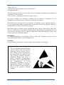
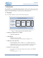
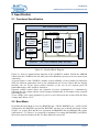
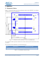
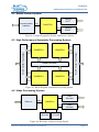
Hardware User Manual CM-BF561 V2.0 Tinyboards from Bluetechnix www.bluetechnix.com Contact Bluetechnix Mechatronische Systeme GmbH Waidhausenstr. 3/19 A-1140 Vienna AUSTRIA/EUROPE [email protected] http://www.bluetechnix.com Document No.: 100-1211-2.0 Document Revision 11 Date: 2009-03-19 Blackfin CM‐BF561 Hardware User Manual Table of Contents 1 Introduction ......................................................................................................................... 1 1.1 Overview ....................................................................................................................... 1 1.2 Differences between Board Versions V1.x ................................................................... 2 1.3 Key Features ................................................................................................................. 2 1.4 Target Applications ....................................................................................................... 2 1.5 Further Information ....................................................................................................... 3 2 Specification ........................................................................................................................ 4 2.1 Functional Specification ............................................................................................... 4 2.2 Boot Mode .................................................................................................................... 4 2.3 Memory Map ................................................................................................................ 5 2.4 Electrical Specification ................................................................................................. 5 2.4.1 Supply Voltage ....................................................................................................... 5 2.4.2 Supply Voltage Ripple ........................................................................................... 5 2.4.3 Input Clock Frequency ........................................................................................... 5 2.4.4 Supply Current ....................................................................................................... 5 2.4.5 Core Voltage and Frequency Requirements........................................................... 5 2.5 Environmental Specification ......................................................................................... 6 2.5.1 Temperature ........................................................................................................... 6 2.5.2 Humidity................................................................................................................. 6 3 CM-BF561 ........................................................................................................................... 7 3.1 Mechanical Outline ....................................................................................................... 7 3.1.1 Footprint ................................................................................................................. 8 3.1.2 Top Mounted Components ..................................................................................... 9 3.2 Schematic Symbol (Signals of P1 and P2) ................................................................. 10 3.3 Connector X1 – (1-60) ................................................................................................ 11 3.4 Connector X2 – (61-120) ............................................................................................ 12 3.5 Optional Expansion Connector X3 – (1-16) ............................................................... 14 3.6 Reset circuit ................................................................................................................ 15 4 Application Examples ....................................................................................................... 16 4.1 Sample Application ..................................................................................................... 16 4.2 Stereo Camera System ................................................................................................ 17 4.3 High Performance Symmetric Processing System ..................................................... 17 4.4 Video Processing System ............................................................................................ 17 4.5 Design Services ........................................................................................................... 18 Blackfin CM‐BF561 Hardware User Manual 5 Software Support ............................................................................................................... 19 5.1 BLACKSheep ............................................................................................................. 19 5.2 uClinux ........................................................................................................................ 19 6 Anomalies .......................................................................................................................... 20 7 Production Report for CM-BF561 (100-1211).................................................................. 21 8 Product Changes ................................................................................................................ 22 9 Document Revision History .............................................................................................. 23 A List of Figures and Tables ................................................................................................. 24 Blackfin CM‐BF561 Hardware User Manual Edition 2007-02 © Bluetechnix Mechatronische Systeme GmbH 2007 All Rights Reserved. The information herein is given to describe certain components and shall not be considered as a guarantee of characteristics. Terms of delivery and rights of technical change reserved. We hereby disclaim any warranties, including but not limited to warranties of noninfringement, regarding circuits, descriptions and charts stated herein. Bluetechnix makes and you receive no warranties or conditions, express, implied, statutory or in any communication with you. Bluetechnix specifically disclaims any implied warranty of merchantability or fitness for a particular purpose. Bluetechnix takes no liability for any damages and errors causing of the usage of this board. The user of this board is responsible by himself for the functionality of his application. He is allowed to use the board only if he has the qualification. More information is found in the General Terms and Conditions (AGB). Information For further information on technology, delivery terms and conditions and prices please contact Bluetechnix (http://www.bluetechnix.com). Warnings Due to technical requirements components may contain dangerous substances. The Core Modules and development systems contain ESD (electrostatic discharge) sensitive devices. Electrostatic charges readily accumulate on the human body and equipment and can discharge without detection. Permanent damage may occur on devices subjected to high-energy discharges. Proper ESD precautions are recommended to avoid performance degradation or loss of functionality. Unused Core Modules and Development Boards should be stored in the protective shipping package. Blackfin CM‐BF561 Hardware User Manual BLACKFIN Products Core Modules: CM-BF533: Blackfin Processor Module powered by Analog Devices single core ADSP-BF533 processor; up to 600MHz, 32MB RAM, 2MB Flash, 120 pin expansion connector and a size of 36.5x31.5mm CM-BF537E: Blackfin Processor Module powered by Analog Devices single core ADSP-BF537 processor; up to 600MHz, 32MB RAM, 4MB Flash, integrated TP10/100 Ethernet physical transceiver, 120 pin expansion connector and a size of 36.5x31.5mm CM-BF537U: Blackfin Processor Module powered by Analog Devices single core ADSP-BF537 processor; up to 600MHz, 32MB RAM, 4MB Flash, integrated USB 2.0 Device, 120 pin expansion connector and a size of 36.5x31.5mm (will be replaced by CM-BF527). TCM-BF537: Blackfin Processor Module powered by Analog Devices single core ADSP-BF537 processor; up to 500MHz, 32MB RAM, 8MB Flash, 28x28mm, 120 pin expansion connector, Ball Grid Array or Border Pads for reflow soldering, industrial temperature range -40°C to +85°C. CM-BF561: Blackfin Processor Module powered by Analog Devices dual core ADSP-BF561 processor; up to 2x 600MHz, 64MB RAM, 8MB Flash, 120 pin expansion connector and a size of 36.5x31.5mm. CM-BF527: The new Blackfin Processor Module is powered by Analog Devices single core ADSP-BF527 processor; key features are USB OTG 2.0 and Ethernet. The 2x60 pin expansion connectors are backwards compatible with other Core Modules. CM-BF548: The new Blackfin Processor Module is powered by Analog Devices single core ADSP-BF548 processor; key features are 64MB DDR SD-RAM 2x100 pin expansion connectors. Development Boards: EVAL-BF5xx: Low cost Blackfin processor Evaluation Board with one socket for any Bluetechnix Blackfin Core Module. Additional peripherals are available, such as an SD-Card. DEV-BF5xxDA-Lite: Get ready to program and debug Bluetechnix Core Modules with this tiny development platform including a USB Based Debug Agent. The DEV-BF5xxDA-Lite is a low cost starter development system including VDSP++ Evaluation Software License. Blackfin CM‐BF561 Hardware User Manual DEV-BF5xx-FPGA: Blackfin Development Board with two sockets for any combination of Blackfin Core Modules. Additional peripherals are available, such as SD-Card, Ethernet, USB host, multi-port JTAG including a USB based Debug Agent, connector for an LCD-TFT Display and connector for a digital camera system. A large on-board SPARTAN-3 FPGA and Soft IPs make this board the most flexible Blackfin development platforms ever developed. DEV-BF548DA-Lite: Get ready to program and debug Bluetechnix CM-BF548 Core Module with this tiny development platform including a USB Based Debug Agent. The DEV-BF548DA-Lite is a low cost starter development system including VDSP++ Evaluation Software License. EXT-Boards: The following Extender Boards are available: EXT-BF5xx-Audio, EXT-BF5xx-Video, EXT-BF5xx-Camera, EXT-BF5xx-Exp, EXTBF5xx-ETH-USB, EXT-BF5xx-AD/DA. Additional boards based on customer request are also available. Software Support: BLACKSheep: The BLACKSheep VDK is a multithreaded framework for the Blackfin processor family from Analog Devices that includes driver support for a variety of hardware extensions. It is based on the realtime VDK kernel included within the VDSP++ development environment. LabVIEW: LabVIEW embedded support for the CM-BF537E, CM-BF537U and TCM-BF537 Core Modules is based upon the BLACKSheep VDK driver Framework. uClinux: All the Core Modules are fully supported by uClinux. The required boot loader and uClinux can be downloaded from: http://blackfin.uClinux.org. Upcoming Products and Software Releases: Keep up-to-date with all the changes to the Bluetechnix product line and software updates at: www.bluetechnix.com BLACKFIN Design Service Based on more than five years of experience with Blackfin, Bluetechnix offers development assistance as well as custom design services and software development. Blackfin CM‐BF561 Hardware User Manual Tinyboards maximum performance at minimum size 1 Introduction The CM-BF561 is an outstanding high performance and low power dual core processor module incorporating Analog Devices Blackfin family of processors. The module allows easy integration into high demanding very space and power limited applications. 1.1 Overview The Core Module CM-BF561 consists of the following components: Dynami Core Voltage Contro BF 561 Up to 600 MHz 64 MByte SDRam 8 MByte Flash Low Voltage Rese 16 Pin Connector 60 Pin Expansion Connector 60 Pin Expansion Connector Figure 1-1: Main components of the CM-BF561 module Analog Devices Blackfin Processor BF561 o ADSP-BF561SKBCZ600 64 MB SDRAM o SDRAM Clock up to 133MHz o 2x MT48LC16M16A2BG-75IT:D (16Mx16, 256Mbit at 3.3V) 8 MB of Byte Addressable Flash o PF48F2000P0ZBQ0 (4Mx16, 64Mbit at 3.3V; all 8MByte addressable) o Additional flash memory can be connected through the expansion board as parallel Flash using asynchronous chip select lines or as a SPI flash. Dynamic Core Voltage Control o Core voltage can be adjusted by setting software registers on the Blackfin processor o Core voltage range: 0.8 – 1.2V Blackfin CM‐BF561 Hardware User Manual Page 1 Tinyboards maximum performance at minimum size Low Voltage Reset Circuit o Resets module if power supply goes below 2.93V for at least 140ms Connector P1 o o o o o o SPORT 0 JTAG UART SPI PPI-1 (Parallel Port Interface 1) GPIO’s Connector P2 o o o o Data Bus Address Bus, Control Signals PPI-2 (Parallel Port Interface 2) Power Supply Expansion Connector P3 o SPORT 1 o PF Flags 1.2 Differences between Board Versions V1.x Version 2.0 and higher differ from Version 1.x in the amount of RAM and FLASH. Both versions are size and PIN Compatible! An additional expansion connector P3 has been provided. The V1.x hardware is not supported any longer. Changes include the removal of the BGA pads and the increase in RAM memory (2x 32MB Chips, providing a total of 64MB) and FLASH memory (Intel P30 8MB instead of Intel J3 4MB) This document contains information of Version 2.x hardware only. See Chapter 7 for Software Changes. 1.3 Key Features The CM-BF561 is very compact and measures only 36.5x31.5 mm Allows quick prototyping of product that comes very close to the final design Reduces development costs, faster time to market Very cost effective for small and medium volumes 1.4 Target Applications Generic high performance signal processor module High performance web camera Robotics: Tiny processor module for mobile robots Blackfin CM‐BF561 Hardware User Manual Page 2 Tinyboards maximum performance at minimum size 1.5 Further Information Further information, and document updates are available on the product homepage: http://www.bluetechnix.com/goto/cm-bf561 Blackfin CM‐BF561 Hardware User Manual Page 3 Tinyboards maximum performance at minimum size 2 Specification 2.1 Functional Specification Mem. Control, Boot Mode, JTAG 32 Data Bus Power Supply Dynamic Core Voltage Control 64 MByte SDRam BF561 up to 600 MHz 2x32MB Chips Low Voltage Reset Clock 16 8 MByte Flash Address Bus Clock-out PPI-1, PPI-2, SPORT0, UART, SPI, GPIO Figure 2-1: Detailed Block Diagram Figure 2-1 shows a detailed block diagram of the CM-BF561 module. Beside the SDRAM control pins the CM-BF561 has all other pins of the Blackfin processor at its two main 60 pin connectors. A special feature of the CM-BF561 module is the availability of two parallel port interfaces (PPI) for different applications such as the simultaneous use of one camera and one display interface; the use of one stereo camera interface; or the use of two separate ports for bandwidth-hungry ADC and DAC interfaces. Dynamic voltage control allows the reduction of power consumption to a minimum by adjusting the core voltage and the clock frequency dynamically in accordance to the required processing power. A low voltage reset circuit guarantees a power on reset and resets the system when the input voltage drops below 2.93V. 2.2 Boot Mode By default the Boot Mode is set to 01 (BMODE0 pin = HIGH, BMODE1 pin = LOW). In this configuration the BMODE0 pin and the BMODE1 pin have an on-board pull-down resistor (Figure 3-4, resistor R10 and R11 are mounted) and BMODE0 has an additional 0R resistor connected to 3.3V (Figure 3-4, resistor R8 is mounted). For setting the BMODE1 pin HIGH a 0R resistor must be mounted at R9. For Boot Mode 00 remove R8. Blackfin CM‐BF561 Hardware User Manual Page 4 Tinyboards maximum performance at minimum size 2.3 Memory Map Memory Type FLASH *) SDRAM Start Address 0x20000000 0x00000000 End Address 0x207FFFFF 0x03FFFFFF Size 8MB 64MB Comment Intel PF48F2000P0ZBQ0 32Bit Bus, 2x Micron MT48LC16M16A2BG Table 2-1: Memory Map *) Please be aware that you have to unlock the flash before starting an erase process! 2.4 Electrical Specification 2.4.1 Supply Voltage 3.3V DC +/-10% 2.4.2 Supply Voltage Ripple 100mV peak to peak 0-20 MHz 2.4.3 Input Clock Frequency 25MHz 2.4.4 Supply Current Maximum supply current: 550mA at 3.3V and 1.2V Core Voltage Operating conditions: o Both core CPUs running at 600MHz, Core Voltage 1.21V, SDRAM 20% bandwidth utilization @ 120MHz: ca. 470mA o Both core CPUs running at 300MHz, Core Voltage 0.8V SDRAM 20% bandwidth utilization @ 100MHz: ca. 160mA o One core CPUs running at 500MHz, Core Voltage 1.16V SDRAM 20% bandwidth utilization @ 125MHz, other core idle: ca. 330mA All measurements done at an environmental temperature of 25°C. 2.4.5 Core Voltage and Frequency Requirements Core voltage: 1.21V Core clock frequency: 500 MHz (default setting) Be aware that the core voltage set in the VR_CTL register doesn’t match exactly with the effective core voltage measured. There is a difference of about 50mV, which is caused by the processor itself. Don’t operate the core module higher than these ratings without cooling otherwise there is a risk of overheating! Blackfin CM‐BF561 Hardware User Manual Page 5 Tinyboards maximum performance at minimum size 2.5 Environmental Specification 2.5.1 Temperature Operating at full 500MHz:: 0 to + 70° C Industrial temperature range on request only Please be aware to operate the CM-BF561 in an environment with enough cooling. If you mount the core module in an enclosure please be aware that there is enough air flow. If an adequate air flow cannot be guaranteed we recommend the use of a heat sink or to reduce the core voltage and/or the core clock frequency. 2.5.2 Humidity Operating: 10% to 90% (non condensing) Blackfin CM‐BF561 Hardware User Manual Page 6 Tinyboards maximum performance at minimum size 3 CM-BF561 3.1 Mechanical Outline Figure 3-1 shows the bottom view of the mechanical outline of the CM-BF561 Core Module. All dimensions are given in millimeters! Figure 3-1: Mechanical outline and Bottom Connectors (bottom view) The mechanical outline represents a bottom view of the connectors placed at the bottom of the core board. The connectors on the CM-BF561 are of the following type: Part X1, X2 X3 Manufacturer Hirose 3mm height Molex FCC/FPC Connector Manufacturer Part No. FX8‐60P‐SV(21) 527451696 Table 3-1: Core Module Connector Types Blackfin CM‐BF561 Hardware User Manual Page 7 Tinyboards maximum performance at minimum size Figure 3-2: Side view with connector mounted The total minimum mounting height including receptacle at the motherboard is 6.1mm. 3.1.1 Footprint The optional 16 pole extension connector may be omitted if there is no need for the additional GPIO pins (see chapter 3.5). Figure 3-3: Recommended footprint and spacing (top view) For the base board the following connectors have to be used. Matching Connector X1,X2 X3 Manufacturer Hirose Molex FCC/FPC Connector Manufacturer Part No. FX8‐60S‐SV 527451696 Table 3-2: Base Board Connector Types Info: A Library of the Baseboards module for the Altium Designer 6.x can be obtained from Bluetechnix upon request. Blackfin CM‐BF561 Hardware User Manual Page 8 Tinyboards maximum performance at minimum size 3.1.2 Top Mounted Components Figure 3-4: Top Overlay (top view) See section 2.2 for the Boot Mode settings. The resistors R1 and R2 switch between Clk_out (R1 mounted, default) and PF11 (R2 mounted) on pin 5 of the Core Module. By mounting a 0R resistor at R6 you can write-protect the on-board flash. Blackfin CM‐BF561 Hardware User Manual Page 9 Tinyboards maximum performance at minimum size 3.2 Schematic Symbol (Signals of P1 and P2) 1 60 2 59 3 58 4 57 5 56 6 55 7 54 8 53 9 52 10 51 11 50 12 49 13 48 14 47 15 46 16 45 17 44 18 43 19 42 20 41 21 40 22 39 23 38 24 37 25 36 26 35 27 34 28 33 29 32 30 31 RSCLK0 / PF28 RFS0 / PF19 DR0PRI DR0SEC / PF20 TSCLK0 / PF29 TFS0 / PF16 DT0PRI / PF18 DT0SEC / PF17 PF11 (CLK-out) PF10 PF9 PF8 PF7 / SPICS7 / TMR7 PF6 / SPICS6 / TMR6 PF5 / SPICS5 / TMR5 PF4 / SPICS4 / TMR4 Vin GND Vin GND PPI1D0 PPI1D1 PPI1D2 PPI1D3 PPI1D4 PPI1D5 PPI1D6 PPI1D7 PPI1D8 / PF40 PPI1D9 / PF41 PPI1D10 / PF42 PPI1D11 / PF43 PPI1D12 / PF44 PPI1D13 / PF45 PPI1D14 / PF46 PPI1D15 / PF47 PPI1Sy3 PPI1Sy2 / TMR9 PPI1Sy1 / TMR8 PPI1Clk PF3 / SPICS3 / TMR3 PF2 / SPICS2 / TMR2 PF1 / SPICS1 / TMR1 PF0 / SPISS / TMR0 RX / PF27 TX / PF26 MOSI MISO SCK ABE0 ABE2 ABE1 ARDY AMS3 TCK TDO TDI TMS TRST EMU CM-BF561 ABE3 A2 A3 A4 A5 A6 A7 A8 A9 A10 A11 A12 A13 A14 A15 PPI2Clk PPI2Sy1 PPI2Sy3 PPI2Sy2 PPI2D0 PPI2D1 PPI2D2 PPI2D3 PPI2D4 PPI2D5 PPI2D6 PPI2D7 PF32 / PPI2D8 PF33 / PPI2D9 PF34 / PPI2D10 PF35 / PPI2D11 PF36 / PPI2D12 PF37 / PPI2D13 PF38 / PPI2D14 PF39 / PPI2D15 N.C. GND AMS2 AMS1 ARE AWE AOE NMI_0 RESET D0 D1 D2 D3 D4 D5 D6 D7 D8 D9 D10 D11 D12 D13 D14 D15 61 120 62 119 63 118 64 117 65 116 66 115 67 114 68 113 69 112 70 111 71 110 72 109 73 108 74 107 75 106 76 105 77 104 78 103 79 102 80 101 81 100 82 99 83 98 84 97 85 96 86 95 87 94 88 93 89 92 90 91 Figure 3-5: Schematic Symbol of the CM-BF561 Module Blackfin CM‐BF561 Hardware User Manual Page 10 Tinyboards maximum performance at minimum size 3.3 Connector X1 – (1-60) Please mind the mounted pull up and pull down resistors on the Core Module (see the third column). Pin No. Signal Signal Type. I/O I I/O I/O I/O I/O I/O I/O PWR PWR I/O I/O I/O I/O I/O I/O I/O I/O I/O I/O I/O I/O I/O – 100k pull up I/O I/O O I – 10k pull up I – 10k pull up I – 10k pull up I – 4k7 pull down O I – 10k pull up O O O O I/O I/O I/O I/O I I/O 1 2 3 4 5 6 7 8 9 10 11 12 13 14 15 16 17 18 19 20 21 22 23 24 25 26 27 28 29 30 31 32 33 34 35 36 37 38 39 40 41 42 RSCLK0 / PF28 DR0PRI TSCLK0 / PF29 DT0PRI / PF18 PF11(Clk_out)* PF9 PF7 / SPISEL7 / TMR7 PF5 / SPISEL5 / TMR5 Vin 3V3 Vin 3V3 PPI1D0 PPI1D2 PPI1D4 PPI1D6 PPI1D8 / PF40 PPI1D10 / PF42 PPI1D12 / PF44 PPI1D14 / PF46 PPI1SYNC3 PPI1SYNC1 / TMR8 PF3 / SSEL3 / TM3 PF1 / SSEL1 / TMR1 RX / PF27 MOSI SCK ABE2 / SDQM2 ARDY TCK TDI TRST EMU TMS TDO AMS3 ABE1/SDQM1 ABE0/SDQM0 MISO TX / PF26 PF0/SPISS/TMR0 PF2/SSEL2/TMR2 PPI1CLK PPI1SYNC2 / TMR9 Blackfin CM‐BF561 Hardware User Manual Page 11 Tinyboards 43 44 45 46 47 48 49 50 51 52 53 54 55 56 57 58 59 60 PPI1D15 / PF47 PPI1D13 / PF45 PPI1D11 / PF43 PPI1D9 / PF41 PPI1D7 PPI1D5 PPI1D3 PPI1D1 GND GND PF4/SPISEL4/TMR4 PF6/SPISEL6/TMR6 PF8 PF10 DT0SEC / PF17 TFS0 / PF16 DR0SEC / PF20 RFS0 / PF19 maximum performance at minimum size I/O I/O I/O I/O I/O I/O I/O I/O PWR PWR I/O I/O I/O I/O O I/O I I/O Table 3-3: Connector P1 Pin Assignment All pin names of the connectors correspond to the names found in the Blackfin BF561 datasheet from Analog Devices. *Mount option R1 and R2: Default is R2 mounted - PF11 at the pin 5 of the connector; unmounting R2 and mounting to position R1 outputs the buffered clock on pin 5 of the connector. (See Figure 3-4) 3.4 Connector X2 – (61-120) Please mind the mounted pull up and pull down resistors on the Core Module (see the third column). Pin No. Signal Signal Type. O O O O O O O O I/O I/O I/O I/O I/O I/O 61 62 63 64 65 66 67 68 69 70 71 72 73 74 ABE3/SDQM3 A3 A5 A7 A9 A11 A13 A15 PPI2SYNC1 PPI2SYNC2 PPI2D1 PPI2D3 PPI2D5 PPI2D7 Blackfin CM‐BF561 Hardware User Manual Page 12 Tinyboards 75 76 77 78 79 80 81 82 83 84 85 86 87 88 89 90 91 92 93 94 95 96 97 98 99 100 101 102 103 104 105 106 107 108 109 110 111 112 113 114 115 116 117 118 119 120 PPI2D9 / PF33 PPI2D11 / PF35 PPI2D13 / PF37 PPI2D15 / PF39 GND AMS1 തതതതതത AWE NMI_0 D0 D2 D4 D6 D8 D10 D12 D14 D15 D13 D11 D9 D7 D5 D3 D1 തRESE തതതതതതതT തതതതത AOE തതതതത ARE തതതതതതത AMS2 N.C. PPI2D14 / PF38 PPI2D12 / PF36 PPI2D10 / PF34 PPI2D8 / PF32 PPI2D6 PPI2D4 PPI2D2 PPI2D0 PPI2SYNC3 PPI2CLK A14 A12 A10 A8 A6 A4 A2 maximum performance at minimum size I/O I/O I/O I/O PWR O O I ‐ 10k pull down I/O I/O I/O I/O I/O I/O I/O I/O I/O I/O I/O I/O I/O I/O I/O I/O I – see chapter 3.6 O O O ‐ I/O I/O I/O I/O I/O I/O I/O I/O I/O I O O O O O O O Table 3-4: Connector P2 Pin Assignment Blackfin CM‐BF561 Hardware User Manual Page 13 Tinyboards maximum performance at minimum size 3.5 Optional Expansion Connector X3 – (1-16) There is an optional expansion connector mounted on the bottom side of the Core Module. He makes accessible some more GPIO pins via a 16 pol FFC (flat flex cable). See the following Symbol and Table for detail information. Pin No. Signal Signal Type. 121 122 123 124 125 126 127 128 129 130 131 132 133 134 135 136 PWR I/O PWR I/O I/O I/O I/O I/O I/O I/O I/O I/O I/O I/O I/O PWR GND SCLK0 GND RSCLK1/PF30 RFS1/PF24 DR1PRI DR1SEC/PF25 TSCLK1/PF31 TFS1/PF21 DT1PRI/PF23 DT1SEC/PF22 PF15/EXTCLK PF14 PF13 PF12 GND Table 3-5: Optional Connector X3 Pin Assignment U1B 122 124 128 126 127 130 131 129 125 132 133 134 135 SCLK0 RSCLK1/PF30 TSCLK1/PF31 DR1PRI DR1SEC/PF25 DT1PRI/PF23 DT1SEC/PF22 TFS1/PF21 RFS1/PF24 PF15/EXTCLK PF14 PF13 PF12 GND GND GND 123 121 136 CM‐BF561‐X Figure 3-6: Optional Extension Connector Symbol Blackfin CM‐BF561 Hardware User Manual Page 14 Tinyboards maximum performance at minimum size 3.6 Reset circuit The reset of the flash and the processor are connected to a power monitoring IC. The output can be used as power on reset for external devices, see Figure 3-7. 3.3V RESET of Flash TCM809SENB713 3 1 VDD RESET GND 2 R12 RESET of ADSP-BF5xx 470R U5 Core Module 99 GND External RESET Figure 3-7: Schematic of reset circuit on the Core Module Blackfin CM‐BF561 Hardware User Manual Page 15 Tinyboards maximum performance at minimum size 4 Application Examples 4.1 Sample Application In this sample application the Core Module is used as a high performance SPI based coprocessor module. U1A 1 60 2 59 3 58 4 57 5 56 6 55 7 54 8 53 9 52 10 51 11 50 12 49 13 48 14 47 15 46 16 45 17 44 18 43 19 42 20 41 21 40 22 39 23 38 24 37 25 36 26 35 27 34 28 33 29 32 30 31 3.3V 3.3V P2 3.3V SPI INTERFACE R1 4k7 SPI_CS 5 4 3 2 1 MOSI MISO SCK MHDR1X5 P1 1 2 3 4 5 6 7 8 9 10 11 12 13 14 EMU TMS TCK TRST TDI TDO Header 7X2 RSCLK0 / PF28 RFS0 / PF19 DR0PRI DR0SEC / PF20 TSCLK0 / PF29 TFS0 / PF16 DT0PRI / PF18 DT0SEC / PF17 PF11 (CLK-out) PF10 PF9 PF8 PF7 / SPICS7 / TMR7 PF6 / SPICS6 / TMR6 PF5 / SPICS5 / TMR5 PF4 / SPICS4 / TMR4 Vin GND Vin GND PPI1D0 PPI1D1 PPI1D2 PPI1D3 PPI1D4 PPI1D5 PPI1D6 PPI1D7 PPI1D8 / PF40 PPI1D9 / PF41 PPI1D10 / PF42 PPI1D11 / PF43 PPI1D12 / PF44 PPI1D13 / PF45 PPI1D14 / PF46 PPI1D15 / PF47 PPI1Sy3 PPI1Sy2 / TMR9 PPI1Sy1 / TMR8 PPI1Clk PF3 / SPICS3 / TMR3 PF2 / SPICS2 / TMR2 PF1 / SPICS1 / TMR1 PF0 / SPISS / TMR0 RX / PF27 TX / PF26 MOSI MISO SCK ABE0 ABE2 ABE1 ARDY AMS3 TCK TDO TDI TMS TRST EMU CM-BF561 ABE3 A2 A3 A4 A5 A6 A7 A8 A9 A10 A11 A12 A13 A14 A15 PPI2Clk PPI2Sy1 PPI2Sy3 PPI2Sy2 PPI2D0 PPI2D1 PPI2D2 PPI2D3 PPI2D4 PPI2D5 PPI2D6 PPI2D7 PF32 / PPI2D8 PF33 / PPI2D9 PF34 / PPI2D10 PF35 / PPI2D11 PF36 / PPI2D12 PF37 / PPI2D13 PF38 / PPI2D14 PF39 / PPI2D15 N.C. GND AMS2 AMS1 ARE AWE AOE NMI_0 RESET D0 D1 D2 D3 D4 D5 D6 D7 D8 D9 D10 D11 D12 D13 D14 D15 61 120 62 119 63 118 64 117 65 116 66 115 67 114 68 113 69 112 70 111 71 110 72 109 73 108 74 107 75 106 76 105 77 104 78 103 79 102 80 101 81 100 82 99 83 98 84 97 85 96 86 95 87 94 88 93 89 92 90 91 CM‐BF561‐X JTAG INTERFACE Figure 4-1: Sample Application with SPI and JTAG Connector, no more pins required. Blackfin CM‐BF561 Hardware User Manual Page 16 Tinyboards maximum performance at minimum size 4.2 Stereo Camera System Communication Interface SPI PPI1 Camera LEFT PPI2 Camera RIGHT CM-BF561 UART Figure 4-2: Image Recognition System with Stereo Cameras 4.3 High Performance Symmetric Processing System PPI1 PPI5 CM-BF561 PPI2 PPI6 Quad Port RAM PPI7 PPI3 CM-BF561 Multi Channel Input/Output Multi Channel Input/Output CM-BF561 CM-BF561 PPI8 PPI4 Figure 4-3: Block Diagram: Symmetric Processing System 4.4 Video Processing System Ethernet D&A PPI1 Video Decoder PPI2 Video Encoder CM-BF561 Bus SD-Card CF-Card Figure 4-4: Real-time Video Processing System Blackfin CM‐BF561 Hardware User Manual Page 17 Tinyboards maximum performance at minimum size 4.5 Design Services Bluetechnix offers custom design services and software development. Blackfin CM‐BF561 Hardware User Manual Page 18 Tinyboards maximum performance at minimum size 5 Software Support 5.1 BLACKSheep The Core Module is delivered with a pre-flashed basic version of the BLACKSheep VDK multithreaded framework. It contains a boot-loader for flashing the Core Module via the serial port. Please mind the software development documents. 5.2 uClinux The Core Module is fully supported by the open source platform at http://blackfin.uclinux.org. Since the Core Modules are pre-flashed with BLACKSheep you have to flash uBoot first. To flash uBoot you can use the BLACKSheep boot-loader. Blackfin CM‐BF561 Hardware User Manual Page 19 Tinyboards maximum performance at minimum size 6 Anomalies For the latest information regarding anomalies for this product, please consult the product home page: http://www.bluetechnix.com/goto/cm-bf561 Blackfin CM‐BF561 Hardware User Manual Page 20 Tinyboards maximum performance at minimum size 7 Production Report for CM-BF561 (100-1211) Version V1.2 V2.0 R20-1000 to R20-2999 V2.0 R20-3000 to R20-3210 V2.0.5 Component Processor RAM FLASH Processor RAM FLASH Processor RAM FLASH Processor RAM FLASH Type ADSP-BF561SKBCZ600 (Rev 0.3) (Analog Devices) MT48LC16M16A2BG-75IT:D (Micron) PF48F2000P0ZBQ0 (Intel) ADSP-BF561SKBCZ600 (Rev 0.3) MT48LC16M16A2BG-75IT:D (Micron) PF48F2000P0ZBQ0 (Intel) ADSP-BF561SKBCZ600 (Rev 0.5) (Analog Devices) MT48LC16M16A2BG-75IT:D (Micron) PF48F2000P0ZBQ0 (Intel) ADSP-BF561SKBCZ600 (Rev 0.5) (Analog Devices) MT48LC16M16A2BG-75IT:D (Micron) PF48F2000P0ZBQ0 (Intel) Table 7-1: Production Report CM-BF561 Blackfin CM‐BF561 Hardware User Manual Page 21 Tinyboards maximum performance at minimum size 8 Product Changes For the latest product change information please consult the product web-page at: http://www.bluetechnix.com/goto/cm-bf561 Version V1.x to V2.0 Changes 64 Mbit Flash, 64MB RAM instead of 32Mbit Flash and 32MB RAM Additional optional bottom FFC connector with 13 Processor pins Table 8-1: Product Changes How do these changes affect the Software developed for V1.x Modules? Flash chip: The flash chip has changed on CM-BF561V2 to an Intel P30 Flash. If you use write accesses to the flash now you have to unlock the appropriate sectors first by using the unlock command as shown in the c-code segment below: nFlashAddr = (unsigned short *)(FLASH_START_ADDRESS + pa_nSectorAddr); *nFlashAddr = 0x0050; //reset statusregister asm("ssync;"); *nFlashAddr = 0x0060; // unlock command asm("ssync;"); *nFlashAddr = 0x00d0; // confirm unlock command Also be aware that the flash is a bottom Boot which means the first 4 sectors have 32kByte then all sectors have 128kByte as in the J3 Flash. This probably won’t affect your application at all, since you may have read only code in these sections anyway. SDRAM: The SDRAM size on V2 is 64MByte (32Mbyte on V1). If you want to be able to use the upper 32MByte you have to change an entry in the SDRAM BANK CONTROL REGISTER to enable the upper 32MByte: For CM-BF561-V2 (64MByte): EBIU_SDBCTL = 0x0015 For version 1 (32MByte): EBIU_SDBCTL = 0x0013 If 32Mbytes is enough you can leave your V1.x software unchanged. Blackfin CM‐BF561 Hardware User Manual Page 22 Tinyboards maximum performance at minimum size 9 Document Revision History Version 11 10 Date 2008-02-19 2008-12-02 9 8 7 6 5 4 3 2 1 2008-09-03 2008-09-03 2008-08-14 2008-04-30 2007-10-01 2007-05-31 2007-05-23 2007-05-15 2007-04-11 Document Revision NMI pull down added Pull up/down information added Reset circuit added Footprint and mechanical drawings updated Footprint and mechanical drawings updated English checked for spelling, grammar and clarity Chapter 2.2, boot mode settings P3 numbering – picture and table, Flash and SD RAM hints + Chip numbers Updated Fig.1 changed Ra, Rb to R1 R2 in Figures Added Chapter 7 description of possible software changes First release V1.0 of the Document Table 9-1: Revision History Blackfin CM‐BF561 Hardware User Manual Page 23 Tinyboards A maximum performance at minimum size List of Figures and Tables Figures Figure 1-1: Main components of the CM-BF561 module.......................................................... 1 Figure 2-1: Detailed Block Diagram .......................................................................................... 4 Figure 3-1: Mechanical outline and Bottom Connectors (bottom view)................................... 7 Figure 3-2: Side view with connector mounted ......................................................................... 8 Figure 3-3: Recommended footprint and spacing (top view) .................................................... 8 Figure 3-4: Top Overlay (top view) ........................................................................................... 9 Figure 3-5: Schematic Symbol of the CM-BF561 Module ...................................................... 10 Figure 3-6: Optional Extension Connector Symbol ................................................................. 14 Figure 3-7: Schematic of reset circuit on the Core Module ..................................................... 15 Figure 4-1: Sample Application with SPI and JTAG Connector, no more pins required. ....... 16 Figure 4-2: Image Recognition System with Stereo Cameras ................................................. 17 Figure 4-3: Block Diagram: Symmetric Processing System .................................................... 17 Figure 4-4: Real-time Video Processing System ..................................................................... 17 Tables Table 2-1: Memory Map ............................................................................................................ 5 Table 3-1: Core Module Connector Types ................................................................................. 7 Table 3-2: Base Board Connector Types ................................................................................... 8 Table 3-3: Connector P1 Pin Assignment ................................................................................ 12 Table 3-4: Connector P2 Pin Assignment ................................................................................ 13 Table 3-5: Optional Connector X3 Pin Assignment ................................................................ 14 Table 7-1: Production Report CM-BF561 ............................................................................... 21 Table 8-1: Product Changes ..................................................................................................... 22 Table 9-1: Revision History ..................................................................................................... 23 Blackfin CM‐BF561 Hardware User Manual Page 24