1
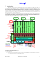
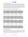
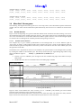
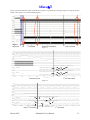
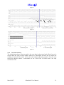
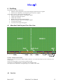
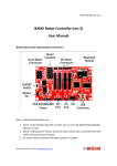
MimoStar3 User Manual MimoStar2 User Manual C. Colledani, W. Dulinski, H. Himmi, Ch. Hu, I.Valin Institut de Recherches Subatomiques IN2P3-CNRS / ULP Strasbourg – France CENTRE NATIONAL DE LA RECHERCHE SCIENTIFIQUE INSTITUT NATIONAL DE PHYSIQUE NUCLEAIRE P HYSIQUE DES P ARTICULES ET DE Mimo Document history Version Date Description 1.0 Based on MimoStar2 Version March 2007 MimoStar chip Version Date 3 Submitted June 06 2 Submitted:June 05 1 Submitted July 04 March 2007 Description AMS 035 Opto Version, 640 x 320 pixels AMS 035 Opto Version, 128 x 128 pixels TSMC 025 Version MimoStar3 User Manual Mimo3 1 2 Introduction ........................................................................................................................ 3 Control Interface ................................................................................................................ 4 2.1 JTAG Instruction Set.................................................................................................. 4 2.2 JTAG Register Set...................................................................................................... 5 2.2.1 Instruction Register ............................................................................................ 5 2.2.2 Bypass Register .................................................................................................. 5 2.2.3 Boundary Scan Register ..................................................................................... 5 2.2.4 ID_CODE Register ............................................................................................ 5 2.2.5 DIS_COL Register ............................................................................................. 6 2.2.6 RO_Mode Register0........................................................................................... 6 2.2.7 BIAS_DAC Register .......................................................................................... 6 3 Running MimoStar3........................................................................................................... 7 3.1 After reset................................................................................................................... 7 3.2 Biasing MimoStar3 .................................................................................................... 7 3.3 Setting the Readout_Mode Register........................................................................... 8 3.4 Readout....................................................................................................................... 8 3.4.1 Signal protocol ................................................................................................... 8 3.4.2 Successive frames and resynchronisation .......................................................... 8 3.5 Analogue Data Format ............................................................................................... 8 3.5.1 Normal mode data format .................................................................................. 9 3.5.2 Test mode data format........................................................................................ 9 3.6 MimoStar3 Chronograms......................................................................................... 10 3.6.1 Normal Readout ............................................................................................... 10 3.6.1.1 Readout synchronisation .............................................................................. 10 3.6.2 Test mode readout ............................................................................................ 12 3.6.3 Main Signal Specifications .............................................................................. 13 3.7 ADC ......................................................................................................................... 13 3.7.1 ADC_SEL register ........................................................................................... 13 4 Pad Ring ........................................................................................................................... 15 4.1 MimoStar3 Pad Ring and Floor Plan View.............................................................. 15 4.2 Pad List..................................................................................................................... 15 March 2007 MimoStar3 User Manual 2 Mimo3 1 Introduction Mimostar3, the third version of the MimoStar family, has been designed in C35B4O1, the AMS 0.35 µm opto process. Like MimoStar 1 and 2, it is a Monolithic Active Pixel Sensor prototype dedicated to vertex particle tracking in a future update of the STAR vertex detector. The matrix is composed by 320 x 640 pixels of 30 µm pitch and based on self biased diode architectures. It is organised in 10 matrices, or subframes, of 320 lines x 64 columns, accessed in parallel during the readout. The individual pixel architecture, should meet the radiation tolerance and the low leakage current requirements. Actually Mimostar3 prototype has the half size of the final circuit which is foreseen with 640 lines. The addressing of each subframe is sequential and starts from the upper left pixel up to the lower right pixel. The beginning of each subframe row is stamped by 2 pixels acting as makers and having programmable levels. The 10 subframes are gathered in 2 banks. Each bank has its own analogue serial output, a differential current output buffer running up to 50 MHz allowing a readout time of 2 ms/frame. Digital Supplies gnd! Bias Tests vdd! Vdd_ADC! gnd! Px<319,639> S u b f r a m e IFASTBUF IFASTINTBUF IAMP IREGAMP IPIX IKIMO 9 Analog Supplies ADC Supplies Vdd_diode! vdda! Px<319,320> Px<319,319> BANK1 S u b f r a m e 5 4 6 7 8 S u b f r a m e Px<319,0> S u b f r a m e BANK0 3 gnd! 2 1 0 ITEST Px<0,639> 5 Colum Address Reg<63:0> 5 Colum Address Reg<63:0> 5 A-Mux 64 to 2 5 A-Mux 64 to 2 Power Supplies CMOS Signals LVDS Signals Analogue Signals BIAS DAC Register<159:0> Disable Colum Register <639:0> BSR <9:0> ADC <7:0> Bias Generators RoMode <7:0> IDCODE JTAG Controller Mi S 3f 10 To 1 AMux ReadOut Controller CKRDP CKRDN SYNC StartADC CkADC 10 To 1 AMux VMUXout<1> AoutP<1> AoutN<1> VMUXin<1:0> M U X Current Refence i RSTMK SSYNC MXFIRST LASTCOL LASTROW CK10M AoutP<0> AoutN<0> VMUXout<0> A vddIn vddaIn Px<0,0> Row Address Register <319:0> RSTB VrpADC Temp Probe TDO TDI TMS TCK TEMP Px<0,320> Px<0,319> l i MimoStar3 is very simple to operate: • Power On Reset or Reset on RSTB pad • Setup of the chip It is performed with programmable registers accessed via an embedded slow control interface. It consists to: • Load the DACs which bias the analogue blocks March 2007 MimoStar3 User Manual 3 Mimo3 • If necessary, load the ReadOut Register with a specific configuration. The default setup on power on reset allows a normal readout once the biases have been set. • Readout of the chip • The chip is driven by a 50 MHz clock. The readout starts when the input "SYNC" token has its falling signal sampled by the internal 5 MHz clock. It happens at the first falling edge of the internal clock which follows the SYNC falling edge. • Readout synchronisation is achieved by the digital marker MxFirst which becomes active when the analogue signal of the first pixel appears • Other digital makers are available for the control of the readout process • Pixels are sequentially read out in a specific order explained later in the document • Successive pixel frames are read until the readout clock is stopped A frame resynchronisation can be performed at any time by setting up the "SYNC" token again. In addition some test features have been implemented in this version: • 2 single-ended voltage output buffers, one per bank, allows a simpler readout at low frequency. The purpose is to verify coarse parameters, like analogue baseline, directly on the wafer with a probe card. • An 8 bit ADC running at 100 kHz/word allows some parameter measurements like voltage supplies and current consumption. • An embedded temperature probe provides its analogue output via 2 output pads. 2 Control Interface The control interface of MimoStar3 complies with the Boundary Scan, JTAG, IEEE 1149.1 Rev 1999 standard. It allows the access to the internal registers of the chip like the bias register and the readout mode selection register. On Power-On-Reset, an internal reset for the control interface is generated. The finite state machine of the Test Access Port (TAP) of the controller enters in the Test-Logic-Reset state and the ID register is selected. 2.1 JTAG Instruction Set The Instruction Register of the JTAG controller is loaded with the code of the desired operation to perform or with the code of the desired data register to access. Instruction EXTEST HIGHZ INTEST CLAMP SAMPLE_PRELOAD ID_CODE BIAS_GEN DIS_COL ADC_SEL ADC_ROR NU1 NU2 NU3 NU4 NU5 NU6 NU7 NU8 NU9 NU10 RO_MODE1 RO_MODE0 BYPASS March 2007 5 Bit Code16 01 02 03 04 05 0E 0F 10 11 12 13 14 15 16 17 18 19 1A 1B 1C 1D 1E 1F Selected Register BSR BYPASS BSR BYPASS BSR ID register BIAS register Disable Columns AnalogIn Select reg ReadOut Register Read Out Mode1 Read Out Mode0 BYPASS Notes JTAG mandatory instruction JTAG optional instruction JTAG optional instruction JTAG optional instruction JTAG mandatory instruction JTAG optional instruction User instruction User instruction User instruction User instruction Reserved, Not Used Reserved, Not Used Reserved, Not Used Reserved, Not Used Reserved, Not Used Reserved, Not Used Reserved, Not Used Reserved, Not Used Reserved, Not Used Reserved, Not Used User instruction User instruction JTAG mandatory instruction MimoStar3 User Manual 4 Mimo3 2.2 JTAG Register Set JTAG registers are implemented with a Capture/Shift register and an Update register. JTAG standard imposes that the last significant bit of a register is downloaded/shifted first. Register Name INSTRUCTION REG BYPASS BSR ID_CODE BIAS_GEN (20 DACs) DIS_COL ADC_SEL ADC_ROR RO_MODE1 RO_MODE0 NU1, …, NU10 Size 5 1 11 32 160 640 20 11 8 8 0 Access R/W R Only R/W R Only R/W R/W R/W R Only R/W R/W Notes Instruction Register Pattern fixed at 0xFFFF0001 Previous value shifted out during write Previous value shifted out during write Previous value shifted out during write Previous ADC value shifted Previous value shifted out during write Previous value shifted out during write Not implemented. For future use 2.2.1 Instruction Register The Instruction register is a part of the Test Access Port Controller defined by the IEEE 1149.1 standard. The Instruction register of MimoStar2 is 5 bits long. On reset, it is set with the ID_CODE instruction. When it is read the 2 last significant bits are set with the markers specified by the standard, the remaining bits contain the current instruction. X X X 1 0 2.2.2 Bypass Register The Bypass register consists of a single bit scan register. It is selected when its code is loaded in the Instruction register, during some actions on the BSR and when the Instruction register contains an undefined instruction. 2.2.3 Boundary Scan Register The Boundary Scan Register, according with the JTAG instructions, tests and set the IO pads. The MimoStar3 BSR is 11 bits long and allows the test of the following input and output pads Bit # 10 9 8 7 6 5 4 3 2 1 0 Corresponding Pad LVDS CkRdP/CkRdN ASync CkADC StartADC SSync Ck5M Ck10M RstMk LastRow LastCol MxFirst Type Input Input Input Input Output Output Output Output Output Output Output Signal CkRd Sync CkADC StarADC SSync Ck5M Ck10M RstMk LastRow LastCol MxFirst Notes Resulting CMOS signal after LVDS Receiver 2.2.4 ID_CODE Register The Device Identification register is implemented is this third version. It is 32 bits long and has fixed value hardwired into the chip. When selected by the ID_CODE instruction or after the fixed value is shifted via TDO, the JTAG serial output of the chip. Mimostar3 ID_CODE register value is 0xFFFF0001 March 2007 MimoStar3 User Manual 5 Mimo3 2.2.5 DIS_COL Register The DIS_COL register is 640 bit wide. The purpose of this register is to disable the column current sources if a short circuit is suspected on a specific column. During the readout, even if a current source is disabled the corresponding column is selected, i.e. no columns are skipped. Obviously, the signal of the corresponding pixel has not signification. The default value of the DIS_COL register is 0; it means that all current sources can be activated by the readout logic. Setting a bit to 1 disables the corresponding current source. In MimoStar2, the column<639> is on the left hand side while column<0> is on the right hand side. The organisation of the chip in 10 subframes of 64 columns has no matter to do with the DIS_COL register. 640 (Msb) DisCol<639> 0 (Lsb) DisCol<0> 2.2.6 RO_Mode Register0 The RO_Mode registers are 8 bits large; they allow the user to select specific features of the chip. MimoStar3 only use RO_Mode Register0. Bit # Bit Name 7 SelJtagCk 6 SelFull 5 DisLVDS 4 SelMux 3 EnaGain3 2 1 0 Not used BufCopy EnaTstCol Purpose Select TCK as the ADC clock in place of the external CkADC signal Set the row shift register to 640 in place of 320 bits. This option is designed to emulate a 640 x 640 pixel matrix. Disable LVDS, readout clock is not active anymore. On MxFirst output, select MuxFirst signal or First_Pixel_of_First_Frame signal Select gain 3 for the serial differential output buffer Default value 0 Ext CkADC selected 0 Normal mode, 320 row shift register selected 0 LVDS selected 1 MuxFirst Signal, active See § 3.4 Readout 0 Gain 5 - Test Mode: Select the 2 Test Levels, IVTEST1 0 Normal mode and IVTEST0, which emulate a pixel output 2.2.7 BIAS_DAC Register The BIAS_DAC register is 160 bits large; it sets simultaneously the 20 DAC registers. As show bellow these 8-bit DACs set voltage and current biases. After reset the register is set to 0, a value which fixes the minimum power consumption of the circuit. The current values of the DACs are read while the new values are downloaded during the access to the register. The image of the value of some critical biases can be measured on corresponding test pads. Bit range 159-152 151-144 DAC # DAC19 DAC18 143-136 DAC17 135-128 127-120 DAC16 DAC15 119-112 111-104 103- 96 95- 88 DAC14 DAC13 DAC12 DAC11 March 2007 DAC Internal DAC purpose Name IKIMO External circuit monitoring I4PIX Pixel source follower bias. DAC with positive slope (0 to 255 µA; 1 µA step) V4TEST1 Test Level, emulates a pixel output. DAC with positive slope (0 to 2.55V; 10 mV step). Marker1 V4TEST0 IDEM. Marker0 V4REG9 Regulator voltage bias for the column amplifier (Gain 3 &5). DAC with negative slope ((3.3 to 0.75 V by step of 10 mV) V4REG8 Idem V4REG7 Idem V4REG6 Idem V4REG5 Idem MimoStar3 User Manual Corresponding Test Pad IKIMO IPIX No pad No pad No pad No pad No pad No pad No pad 6 Mimo3 87- 80 79- 72 71- 64 63- 56 55- 48 47- 40 39- 32 DAC10 DAC9 DAC8 DAC7 DAC6 DAC5 DAC4 V4REG4 V4REG3 V4REG2 V4REG1 V4REG0 I4REG1 I4AMP 31- 24 DAC3 I4INTBUF 23- 16 DAC2 V4BUF1 15- 8 7- 0 DAC1 DAC0 V4BUF0 I4BUF Idem Idem Idem Idem Idem Idem Bias of column amplifier. DAC with positive slope (0 to 255 µA; 1 µA step) Bias of the Intermediate Buffer. DAC with positive slope (0 to 255 µA; 1 µA step) Bias of the differential current Output Buffer. DAC with positive slope (0 to 2.55 V by step of 10 mV) Idem Bias of the two differential current output buffers. DAC with positive slope (0 to 255 µA; 1 µA step) No pad No pad No pad No pad No pad IREGAMP IAMP IFASTINTBUF No pad No pad IFASTBUF 3 Running MimoStar3 The following steps describe how to operate Mimostar3 3.1 After reset On RSTB active low signal: • All BIAS registers are set to the default value, i.e. 0 • DIS_COL is set to 0, i.e. all columns are selected • RO_Mode is set to 0 • JTAG state machine is in the Test-Logic-Reset state • JTAG ID_CODE instruction is selected Then the bias register has to be loaded. The same for the RO_MODE0 and DIS_COL registers if the running conditions differ from defaults. Finally the readout can be performed either in normal mode or in test mode. 3.2 Biasing MimoStar3 The BIAS_DAC register has to be loaded before operating MimoStar3. The 20 DACs constituting this register are built with the same 8 bits DAC current generator which has a 1 µA resolution. Specific interfaces like current mirror for current sourcing or sinking and resistors for voltages, customise each bias output. The following table shows the downloaded codes which set the nominal bias. Internal DAC Name Resol Simulation Code16 - DacInternal Output ution Code10 current-µA value Range Experimental (1) Code16 - Code10 IKIMO 64-100 100 1V 10 mV From 0 up to 2.55 V 0-0 I4PIX 1E-30 30 30 µA 1 µA From 0 up to 255 µA 1-1 V4TEST1 C3–195 195 1.95 V 10 mV From 0 up to 2.55 V FA-250 V4TEST0 B9–185 185 1.85 V 10 mV From 0 up to 2.55 V E6-230 V4REG 9-0 23–35 35 2.95 V 10 mV From 3.3 down to 0.75 V 80-128 I4REG1 21–33 33 33 µA 1 µA From 0 up to 255 µA 1-1 I4AMP 64–100 100 100 µA 1 µA From 0 up to 255 µA 80-128 I4INTBUF 64–100 100 100 µA 1 µA From 0 up to 255 µA 3-3 V4BUF1-0 5C–92 92 0.92 V 10 mV From 0 up to 2.55 V I4BUF 28–40 40 40 µA 1 µA From 0 up to 255 µA Note 1: The HRES polysilicon, used in the bias block, is missing for this submission. Experimental values correspond to the recalculated parameters that allow nevertheless the chip be operated. A new submission of the chip is in progress. March 2007 MimoStar3 User Manual 7 Mimo3 Bias synthetic block diagram I+ Vrefn G=3&5 I- Regulator I4PIX I4TNTBUF V4REGn + - I4REGAMP I4AMP * n = 0, 1, 2, …9 for 10 sub-matrices V4TEST1 + - + - V4BUFm + - I4BUF * m = 0, 1for 2 output buffers V4TEST0 Note1: Vrefn ~= V4REGn – 1V 3.3 Setting the Readout_Mode Register If the desired operating mode does not correspond to the default one, set the Readout_Mode register following the §2.2.6. 3.4 Readout 3.4.1 Signal protocol Ones JTAG registers have been loaded, the readout of MimoStar3 may initiate with the following signal protocol: • The readout clock is started. This allows the CK10M output pad to generate a 10 MHz clock. This clock follows the input clock with a 1/10 ratio if the 100 MHz is selected. • The SYNC signal is set. • The readout starts at the first rising edge of CK10M of after SYNC signal disappears. • Signal markers allow the readout monitoring and the analogue data sampling: o RstMk maker confirms the internal reset of the readout logic. o SSync marker shows that the readout starts. o 4 extra CK10M clock cycles, after SYNC sampling, are necessary before the first pixel analogue signal appears on the selected output(s). o The MxFirst digital signal helps for a better sampling of the analogue output signals. The way it acts is set by the RO_Mode[4] bit. RO_Mode[4] = 0: MxFirst is active only on the first pixel oft the frame RO_Mode[4] = 1: MxFirst is active on each pixel change on the parallel analogue output i.e. it is a10 MHz periodic signal. Used with the 100 MHz serial mode (see serial data format bellow), its period shows when one pixel index has been read in all the subframes (2 real + 8 virtual). o LastCol is active when the last column of the current row is selected o LastRow is active when the last row of the frame is selected 3.4.2 Successive frames and resynchronisation Successive pixel frames are read until the readout clock is stopped. A frame resynchronisation can be performed at any time by setting up the "SYNC" token again. 3.5 Analogue Data Format Two types of signal can be generated on the serial analogue outputs • Normal pixel signal • Test signal March 2007 MimoStar3 User Manual 8 Mimo3 3.5.1 Normal mode data format In order to improve the readout speed Mimostar3 is organized in subframes, i.e. 10 subframes for this prototype. During the readout, the 10 subframes are accessed in parallel. For each subframe the addressing is done row by row, each pixel is accessed sequentially from the left side to right side. Each row contains 2 makers (acting as dummy pixels), and 64 active pixels. One can use the adjustable level of the 2 markers as a pattern recogniser. If the pixel coordinate format is specified as Px<Line, Column>, then for each subframe, the upper left pixel is Px<319, 63> while the lower right is Px<0, 0> and the markers of each beginning row are named Mk1 and Mk0. The 10 subframes are themselves gathered in 2 banks. The two banks are readout in parallel; each one has its own analogue serial output. Thus in each bank, the readout consists to access successively one pixel of each of the 5 subframes and then turning back to the first subframe in order to read its next pixel. For Mimostar3 the left hand side subframe is named Sf9 and the right hand side is Sf0. Thus the normal data stream format for the bank1 on the analogue output<1> is: Sf9Mk1 ,Sf8Mk1 ,Sf7Mk1 ,Sf6Mk1 ,Sf5Mk1 , Sf9Mk0 ,Sf8Mk0 ,Sf7Mk0 ,Sf6Mk0 ,Sf5Mk0 , Sf9Px<319,63>,Sf8Px<319,63>,Sf7Px<319,63>,Sf6Px<319,63>,Sf5Px<319,63>, Sf9Px<319,62>,Sf8Px<319,62>,Sf7Px<319,63>,Sf6Px<319,62>,Sf5Px<319,62>, . . . . . . . . . . . . . . . . . . . . . . . . . . . . . . . . . . . Sf9Px<319, 0>,Sf8Px<319, 0>,Sf7Px<319, 0>,Sf6Px<319, 0>,Sf5Px<319, 0>, Sf9Mk1 ,Sf8Mk1 ,Sf7Mk1 ,Sf6Mk1 ,Sf5Mk1, Sf9Mk0 ,Sf8Mk0 ,Sf7Mk0 ,Sf6Mk0 ,Sf5Mk0, Sf9Px<318,63>,Sf8Px<318,63>,Sf7Px<318,63>,Sf6Px<318,63>,Sf5Px<318,63>, Sf9Px<318,62>,Sf8Px<318,62>,Sf7Px<318,63>,Sf6Px<318,62>,Sf5Px<318,62>, . . . . . . . . . . . . . . . . . . . . . . . . . . . . . . . . . . . Sf9Px<318, 0>,Sf8Px<318, 0>,Sf7Px<318, 0>,Sf6Px<318, 0>,Sf5Px<318, 0>, Sf9Mk1 ,Sf8Mk1 ,Sf7Mk1 ,Sf6Mk1 ,Sf5Mk1 , Sf9Mk0 ,Sf8Mk0 ,Sf7Mk0 ,Sf6Mk0 ,Sf5Mk0 , Sf9Px< 0,63>,Sf8Px< 0,63>,Sf7Px< 0,63>,Sf6Px< 0,63>,Sf5Px< 0,63>, Sf9Px< 0,62>,Sf8Px< 0,62>,Sf7Px< 0,63>,Sf6Px< 0,62>,Sf5Px< 0,62>, . . . . . . . . . . . . . . . . . . . . . . . . . . . . . . . . . . . Sf9Px< 0, 0>,Sf8Px< 0, 0>,Sf7Px< 0, 0>,Sf6Px< 0, 0>,Sf5Px< 0, 0>, For bank0 the format on the analogue output<0> is: Sf4Mk1 ,Sf3Mk1 ,Sf2Mk1 ,Sf1Mk1 ,Sf0Mk1 , Sf4Mk0 ,Sf3Mk0 ,Sf2Mk0 ,Sf1Mk0 ,Sf0Mk0 , Sf4Px<319,63>,Sf3Px<319,63>,Sf2Px<319,63>,Sf1Px<319,63>,Sf0Px<319,63>, Sf4Px<319,62>,Sf3Px<319,62>,Sf2Px<319,63>,Sf1Px<319,62>,Sf0Px<319,62>, . . . . . . . . . . . . . . . . . . . . . . . . . . . . . . . . . . . Sf4Px<319, 0>,Sf3Px<319, 0>,Sf2Px<319, 0>,Sf1Px<319, 0>,Sf0Px<319, 0>, Sf4Mk1 ,Sf3Mk1 ,Sf2Mk1 ,Sf1Mk1 ,Sf0Mk1, Sf4Mk0 ,Sf3Mk0 ,Sf2Mk0 ,Sf1Mk0 ,Sf0Mk0, Sf4Px<318,63>,Sf3Px<318,63>,Sf2Px<318,63>,Sf1Px<318,63>,Sf0Px<318,63>, Sf4Px<318,62>,Sf3Px<318,62>,Sf2Px<318,63>,Sf1Px<318,62>,Sf0Px<318,62>, . . . . . . . . . . . . . . . . . . . . . . . . . . . . . . . . . . . Sf4Px<318, 0>,Sf3Px<318, 0>,Sf2Px<318, 0>,Sf1Px<318, 0>,Sf0Px<318, 0>, Sf4Mk1 ,Sf3Mk1 ,Sf2Mk1 ,Sf1Mk1 ,Sf0Mk1 , Sf4Mk0 ,Sf3Mk0 ,Sf2Mk0 ,Sf1Mk0 ,Sf0Mk0 , Sf4Px< 0,63>,Sf3Px< 0,63>,Sf2Px< 0,63>,Sf1Px< 0,63>,Sf0Px< 0,63>, Sf4Px< 0,62>,Sf3Px< 0,62>,Sf2Px< 0,63>,Sf1Px< 0,62>,Sf0Px< 0,62>, . . . . . . . . . . . . . . . . . . . . . . . . . . . . . . . . . . . Sf4Px< 0, 0>,Sf3Px< 0, 0>,Sf2Px< 0, 0>,Sf1Px< 0, 0>,Sf0Px< 0, 0>, 3.5.2 Test mode data format During the test mode the pixel matrix is not connected to the multiplexing electronic. In place of it, two test levels V4TEST1 (V1), V4TEST0 (V0) are available. . They emulate the readout shift from one column of pixel to the other column of pixel.. Actually these levels correspond to those of Marker 1 and Marker 0. They are adjustable via 2 DACs. Even and odd columns amplifiers are alternatively connected to one of them. The V1 and V1 levels are connected to the multiplexing electronic with a specific patter. This pattern allows seeing the output signal changing Thus the test data stream has the following format: March 2007 MimoStar3 User Manual 9 Mimo3 Analogue output <1> format: Sf9V1, Sf8V0, Sf7V1, Sf6V0, Sf5V1, Sf9V0, Sf8V1, Sf7V0, Sf6V1, Sf5V0, Sf9V0, Sf8V1, Sf7V0, Sf6V1, Sf5V0, Sf9V1, Sf8V0, Sf7V1, Sf6V0, Sf5V1, . . . . . . . . . . Analogue output <0> format: Sf4V0, Sf3V1, Sf2V0, Sf1V1, Sf0V0, Sf4V1, Sf3V0, Sf2V1, Sf1V0, Sf0V1 Sf4V1, Sf3V0, Sf2V1, Sf1V0, Sf0V1, Sf4V0, Sf3V1, Sf2V0, Sf1V1, Sf0V0 . . . . . . . . . . 3.6 MimoStar3 Chronograms The following chronograms describe typical access to the chip; Reset, JTAG download sequence and then the readout. This one starts with the initialisation phase followed by the successive row readouts as showed in the zoom. 3.6.1 Normal Readout Figure 1 show the beginning of a typical normal data readout mode. After Reset and JTAG settings, one can see the initialisation phase of the readout of the first pixel row. The LastCol signal is active meanwhile the last pixel of a row is read. The last row of the frame makes the LastRow signal to be active. The 2 serial analogue outputs are showed. One can distinguish the 2 makers placed at the beginning of each row. 3.6.1.1 Readout synchronisation The simplest way to get a readout synchronisation on the analogue data is to use the MxFirst signal in “First_Pixel_of_Frame” mode which becomes active when the first pixel is ready on the analogue output. It makes the data acquisition independent of the latency which exists between the start of the readout (Sync) and the appearance of the data. Nevertheless if it is impossible for the user to use MxfFirst, the synchronisation on the analogue data is possible by counting the number of the CK10M cycles. The latency between the Sync signal falling edge and the rising edge of the MxFirst signal is: Latency = ( (Ck10Count +1) modulo 2) + 6 Where: • Latency is given in CK10M cycles. It begins at the first Ck10M rising edge which follows the Sync falling edge • Ck10Count is the value of a CK10M counter at the falling edge of SYNC Cursor – Baseline = 600ns 6 clock cycles of latency Baseline = 1212ns Cursor – Baseline = 700ns 400ns 800ns 1200ns 1600ns TimeA = 1912ns 2000ns 2400ns 7 clock cycles of latency Figure 2 zoom on the readout start. After a latency of 6 or 7 CK10M cycles, Mxfirst goes active and the analogue signal generated in respect with the serial format. Figure 3 zoom on the transition between 2 consecutive rows of the same frame. The markers are clearly showed. Figure 4 shows the end of the last row readout followed by the first row of the next frame. March 2007 MimoStar3 User Manual 10 Mimo3 Figure 5 show the alternate option of the MxFirst signal. It is permanently running, being active high on the first maker. This option is set via the RoMode register. <3:0> Reset + Jtag access Idle Init 1rstrow readout Successive row readouts Last row readout Figure 1 Sf4Px<319,63> Sf3Px<319,63> Sf3Px<319,63> Sf4M1,Sf3M1,Sf2M1,Sf1M1,Sf0M1 Sf4M0,Sf3M0,Sf2M0,Sf1M0,Sf0M0 Sf9Px<319,63> Sf8Px<319,63> Sf7Px<319,63> Sf9M1,Sf8M1,Sf7M1,Sf6M1,Sf5M1 <3> Sf9M0,Sf8M0,Sf7M0,Sf6M0,Sf5M0 Initialisation phase 1 rst row readout phase Figure 2 Sf0Px<319,0> Sf4M1,Sf3M1,Sf2M1,Sf1M1,Sf0M1 Sf3Px<318,63> Sf4Px<318,63> Sf5Px<319,0> Sf4M0,Sf3M0,Sf2M0,Sf1M0,Sf0M0 Sf8Px<318,63> Sf9Px<318,63> Sf5Px<319,0> Sf9M1,Sf8M1,Sf7M1,Sf6M1,Sf5M1 End of 1rst row readout March 2007 MimoStar3 User Manual 2nd row readout 11 Mimo3 Figure 3 S f 4 M 1 , S f 3 M 1 , S f 2 M 1 , S f 1 M 1 , S f 0 M1 Sf 1Px <0 ,0 > S f0P x<0 , 0> S f 4 M 0 , S f 3 M 0 , S f 2 M 0 , S f 1 M 0 , S f 0 M0 S f3P x<3 1 9,6 3 > Sf2 Px< 3 19,6 3 > Sf4 Px< 3 19, 63 > E n d o f last row re ado u t N ex t F ram e 1 rst row read ou t Figure 4 Initialisation phase 1rst row readout phase Figure 5 3.6.2 Test mode readout The initialisation phase if the test mode is the same than in the normal mode. But it has to be noticed than the LastCol and LastRow makers are unavailable because the test mode has nothing to deal with the matrix and its line and column addressing registers. For the same reason the MxFirst maker is unavailable in the “First Pixel of frame mode” but only continuous mode. March 2007 MimoStar3 User Manual 12 Mimo3 Sf4V0 Sf2V0 Sf0V0 Sf3V0 Sf1V0 Sf4V1 Sf3V1 Sf1V1 Sf4V1 Sf2V1 Sf0V1 Sf9V1 Sf7V1 Sf5V1 Sf8V1 Sf6MV1 Sf8V0 Sf6V0 Sf9V0 Sf7V0 Sf5V0 Initialisation phase 3.6.3 Repeated pattern Main Signal Specifications Parameter RSTB Pulse Width TCK Frequency JTAG TMS Setup/Hold Time TDI Setup/Hold Time READOUT CKRD Frequency CKRD Duty Cycle SYNC Setup/Hold Time INIT Typical Value >1 μS 10 MHz ~10 nS ~10 nS Up to 50 MHz 50% 5 nS Notes Active Low, Asynchronous Power on Reset Boundary Scan Clock Boundary Scan Control Signal Boundary Scan Serial Data In Readout Clock LVDS signal Chip Initialisation, CMOS signal. Starts after falling edge on 1rst CKRD sampling Input Dynamic range 0.7 up to 1.2 V @ 10-90%, for fully input dynamic range Rise time 5 nS Differential Fall time Simulated with Zload = 2*100 Ohm and 2*5pF 5 nS Current Bandwidth 245 MHz @ -3 dB Buffer (1) Transconductance gain 5.8 mS Output Current Range -2.2; 2.2 mA Note 1: The differential current output buffer can be modelled as an ideal current source. Its performances in terms of raising and falling times are limited by its load’s time constant (Rload x Cload) Note 2: Simple source follower 3.7 3.7.1 ADC ADC_SEL register Bit # 19 18 17 16 15 14 13 12 11 10 9 8 7 March 2007 Selected signal for the measure DAC V4FASTBUF1 DAC V4FASTBUF0 DAC V4REG9 DAC V4REG8 DAC V4REG7 DAC V4REG6 DAC V4REG5 DAC V4REG4 DAC V4REG3 DAC V4REG2 DAC V4REG1 DAC V4REG0 DAC VTEST1 MimoStar3 User Manual 13 Mimo3 6 5 4 3 2 1 0 March 2007 DAC VTEST0 VDDA chip Supply VDDA IN Pad VDDD Chip supply VDDD IN Pad VMUX<1> Pad VMUX<0> Pad MimoStar3 User Manual 14 Mimo3 4 Pad Ring The pad ring of the chip is build with • Pads full custom designed for some of the analogue signals and power supplies • Pads from the AMS library for the digital signals and power supplies The pad ring is split in 7 functional independent parts • Read out analogue output<1> & analogue supplies • CMOS JTAG & digital supplies • LVDS read out drivers • Digital read out control & digital supplies • Read out analogue output<0> & analogue supplies • Test ADC input signals • Test ADC control signals & supplies 4.1 MimoStar3 Pad Ring and Floor Plan View BANK 1 BANK 0 DAC 1 P_A1 P_D1 ADC RdO-Cntl P_L P_D2 P_A2 PAdc1 187 PAdc2 Foundry submission information Mimostar3 has been designed in AMS C35B4O1 CMOS 0.35 μm epitaxial and opto process with 2 poly and 4 metal layers. The Process Design Kit V3.70 has been provided by CMP CAD tools are CADENCE DFII 5.0 with DIVA and ASSURA rules The chip has been submitted in an engineering run via CMP the June 2006 4.2 Pad List March 2007 MimoStar3 User Manual 15 Mimo3 Pad 1 2 3 4 5 6 7 8 9 10 11 12 13 14 15 16 17 18 19 20 21 22 23 24 25 26 27 28 29 30 31 32 33 34 35 36 37 38 39 40 41 42 43 44 45 46 47 48 49 50 51 52 53 Name gnd gnd gnd TEMP IFASTBUF IFASTINBUF IAMP IREGAMP IPIX IKIMO ITEST vdda vdda vdda vdda vdda vdda vdda vdda gnd gnd gnd gnd gnd gnd gnd gnd vdd_diode vdd_diode vdd_diode vdd_diode vdd_diode vdd_diode gnd gnd vdda vdda vdda vdda vdda vdda vdda vdda gnd gnd Aout1P(pb) Aout1P Aout1N Aout1N(pb) VMUXout<1> gnd gnd gnd March 2007 Pad ring segment 1 – P_A1 Pad General Function PadType Core logic and periphery cells supply AGNDALLP Core logic and periphery cells supply AGNDALLP Core logic and periphery cells supply AGNDALLP Direct Pad, no protections DIRECTPAD APRIOP Analog I/O pad, 0 Ω serial APRIOP Analog I/O pad, 0 Ω serial APRIOP Analog I/O pad, 0 Ω serial APRIOP Analog I/O pad, 0 Ω serial APRIOP Analog I/O pad, 0 Ω serial APRIOP Analog I/O pad, 0 Ω serial APRIOP Analog I/O pad, 0 Ω serial Analogue Pad Supply AVDDALLP Analogue Pad Supply AVDDALLP Analogue Pad Supply AVDDALLP Analogue Pad Supply AVDDALLP Analogue Pad Supply AVDDALLP Analogue Pad Supply AVDDALLP Analogue Pad Supply AVDDALLP Analogue Pad Supply AVDDALLP Core logic and periphery cells supply AGNDALLP Core logic and periphery cells supply AGNDALLP Core logic and periphery cells supply AGNDALLP Core logic and periphery cells supply AGNDALLP Core logic and periphery cells supply AGNDALLP Core logic and periphery cells supply AGNDALLP Core logic and periphery cells supply AGNDALLP Core logic and periphery cells supply AGNDALLP Direct Pad, no protections DIRECTPAD Direct Pad, no protections DIRECTPAD Direct Pad, no protections DIRECTPAD Direct Pad, no protections DIRECTPAD Direct Pad, no protections DIRECTPAD Direct Pad, no protections DIRECTPAD Core logic and periphery cells supply AGNDALLP Core logic and periphery cells supply AGNDALLP Analogue Pad Supply AVDDALLP Analogue Pad Supply AVDDALLP Analogue Pad Supply AVDDALLP Analogue Pad Supply AVDDALLP Analogue Pad Supply AVDDALLP Analogue Pad Supply AVDDALLP Analogue Pad Supply AVDDALLP Analogue Pad Supply AVDDALLP Analogue Pad Supply AGNDALLP Analogue Pad Supply AGNDALLP Simple metal for probing Full Custom Empty pad with embedded buffer Full Custom Empty pad with embedded buffer Full Custom Simple metal for probing Full Custom Direct Pad, no protections DIRECTPAD Analogue Pad Supply AGNDALLP Analogue Pad Supply AGNDALLP Analogue Pad Supply AGNDALLP MimoStar3 User Manual Function for the chip Ground periphery & core Ground periphery & core Ground periphery & core Temperature probe output DAC Out, Test Purpose Only DAC Out, Test Purpose Only DAC Out, Test Purpose Only DAC Out, Test Purpose Only DAC Out, Test Purpose Only Gen Purpose DAC Output Internal Current Ref Source Supply periphery & core Supply periphery & core Supply periphery & core Supply periphery & core Supply periphery & core Supply periphery & core Supply periphery & core Supply periphery & core Ground periphery & core Ground periphery & core Ground periphery & core Ground periphery & core Ground periphery & core Ground periphery & core Ground periphery & core Ground periphery & core Pixel Diode Bias, 3.3V Pixel Diode Bias, 3.3V Pixel Diode Bias, 3.3V Pixel Diode Bias, 3.3V Pixel Diode Bias, 3.3V Pixel Diode Bias, 3.3V Ground periphery & core Ground periphery & core Supply periphery & core Supply periphery & core Supply periphery & core Supply periphery & core Supply periphery & core Supply periphery & core Supply periphery & core Supply periphery & core Ground periphery & core Ground periphery & core Differential parallel output<1> Differential parallel output<1> Probing Analogue out, test purpose only Ground periphery & core Ground periphery & core Ground periphery & core 16 Mimo3 54 gnd 55 gnd 56 gnd Pad 57 58 59 60 61 62 63 64 65 66 67 68 69 70 71 72 73 74 75 76 77 78 79 80 81 82 83 84 85 86 87 88 89 90 Pad 91 92 93 94 95 96 97 98 Analogue Pad Supply Analogue Pad Supply Analogue Pad Supply AGNDALLP Ground periphery & core AGNDALLP Ground periphery & core AGNDALLP Ground periphery & core Name vddd vddd vddd vddd vddd vddd RSTB(pb) RSTB vddd vddd TMS(pb) TMS vddd vddd TDI(pb) TDI vddd vddd TCK(pb) TCK gnd gnd TDO(pb) TDO gnd gnd RSTMK(pb) RSTMK gnd gnd gnd gnd gnd gnd Pad ring segment 2 – P_D1 Pad General Function PadType Core logic and periphery cells supply VDD3RP Core logic and periphery cells supply VDD3RP Core logic and periphery cells supply VDD3RP Core logic and periphery cells supply VDD3RP Core logic and periphery cells supply VDD3RP Core logic and periphery cells supply VDD3RP Simple metal for probing Full Custom Schmitt-Trigger Input Buffer, Pull Up ISUP Output buffer supply VDD3OP Output buffer supply VDD3OP Simple metal for probing Full Custom CMOS Input Buffer, Pull Up ICUP Output buffer supply VDD3OP Output buffer supply VDD3OP Simple metal for probing Full Custom CMOS Input Buffer, Pull Up ICUP Output buffer supply VDD3OP Output buffer supply VDD3OP Simple metal for probing Full Custom CMOS Clock Input Buffer, 2 mA ICCK2P Output buffer ground GND3OP Output buffer ground GND3OP Simple metal for probing Full Custom Tri-State Output Buffer, 4 mA BT4P Output buffer ground GND3OP Output buffer ground GND3OP Simple metal for probing Full Custom Tri-State Output Buffer, 2 mA BT2P Core logic and periphery cells gnd GND3RP Core logic and periphery cells gnd GND3RP Core logic and periphery cells gnd GND3RP Core logic and periphery cells gnd GND3RP Core logic and periphery cells gnd GND3RP Core logic and periphery cells gnd GND3RP Name gnd gnd CKRN(pb) CKRN CKRP CKRP(pb) vddd vddd Pad ring segment 3 – P_L Pad General Function PadType Analogue Pad Supply AGNDALLP Analogue Pad Supply AGNDALLP Simple metal for probing Full Custom LVDS In Full Custom LVDS In + Simple metal for probing Full Custom Analogue Pad Supply AVDDALLP Analogue Pad Supply AVDDALLP March 2007 MimoStar3 User Manual Function for the chip Digital supply, periphery & core Digital supply, periphery & core Digital supply, periphery & core Digital supply, periphery & core Digital supply, periphery & core Digital supply, periphery & core Probing Asynchronous Active Low Reset Output buffer supply Output buffer supply Probing JTAG Control Signal Output buffer supply Output buffer supply Probing JTAG Control Signal Output buffer supply Output buffer supply Probing JTAG Clock Output buffer ground Output buffer ground Probing JTAG Serial Data Out Output buffer ground Output buffer ground Probing Readout Reset Marker Digital ground, periphery & core Digital ground, periphery & core Digital ground, periphery & core Digital ground, periphery & core Digital ground, periphery & core Digital ground, periphery & core Function for the chip Ground periphery & core Ground periphery & core Probing Readout Clock Signal Probing Supply periphery & core Supply periphery & core 17 Mimo3 Pad 99 100 101 102 103 104 105 106 107 108 109 110 111 112 113 114 115 116 117 118 119 120 121 122 123 124 125 126 127 128 129 130 131 132 Pad 133 134 135 136 137 138 139 140 141 142 143 144 145 146 147 Name vddd vddd vddd vddd vddd vddd LastRow(pb) LastRow vddd vddd LastCol(pb) LastCol vddd vddd CK10M(pb) CK10M gnd gnd MxFirst(pb) MxFirst gnd gnd Ssync(pb) Ssync gnd gnd Sync(pb) Sync gnd gnd gnd gnd gnd gnd Pad ring segment – P_D2 Pad General Function PadType Core logic and periphery cells supply VDD3RP Core logic and periphery cells supply VDD3RP Core logic and periphery cells supply VDD3RP Core logic and periphery cells supply VDD3RP Core logic and periphery cells supply VDD3RP Core logic and periphery cells supply VDD3RP Simple metal for probing Full Custom Tri-State Output Buffer, 2 mA BT2P Output buffer supply VDD3OP Output buffer supply VDD3OP Simple metal for probing Full Custom Tri-State Output Buffer, 2 mA BT2P Output buffer supply VDD3OP Output buffer supply VDD3OP Simple metal for probing Full Custom Tri-State Output Buffer, 2 mA BT2P Output buffer ground GND3OP Output buffer ground GND3OP Simple metal for probing Full Custom Tri-State Output Buffer, 2 mA BT2P Output buffer ground GND3OP Output buffer ground GND3OP Simple metal for probing Full Custom Tri-State Output Buffer, 2 mA BT2P Output buffer ground GND3OP Output buffer ground GND3OP Simple metal for probing Full Custom CMOS Input Buffer ICP Core logic and periphery cells gnd GND3RP Core logic and periphery cells gnd GND3RP Core logic and periphery cells gnd GND3RP Core logic and periphery cells gnd GND3RP Core logic and periphery cells gnd GND3RP Core logic and periphery cells gnd GND3RP Name gnd gnd gnd gnd gnd gnd VMUX0 Aout0N(pb) Aout0N Aout0P Aout0P(pb) gnd gnd vdda vdda Pad ring segment – P_A2 Pad General Function PadType Analogue Pad Supply AGNDALLP Analogue Pad Supply AGNDALLP Analogue Pad Supply AGNDALLP Analogue Pad Supply AGNDALLP Analogue Pad Supply AGNDALLP Analogue Pad Supply AGNDALLP Direct Pad, no protections DIRECTPAD Simple metal for probing Full Custom Empty pad with embedded buffer Full Custom Empty pad with embedded buffer Full Custom Simple metal for probing Full Custom Analogue Pad Supply AGNDALLP Analogue Pad Supply AGNDALLP Analogue Pad Supply AVDDALLP Analogue Pad Supply AVDDALLP March 2007 MimoStar3 User Manual Function for the chip Digital supply, periphery & core Digital supply, periphery & core Digital supply, periphery & core Digital supply, periphery & core Digital supply, periphery & core Digital supply, periphery & core Probing Last Row Maker Output buffer supply Output buffer supply Probing Last Column Marker Output buffer supply Output buffer supply Probing 20 MHz Clock Out Output buffer ground Output buffer ground Probing First pixel maker Output buffer ground Output buffer ground Probing Readout Synchro. Start Marker Output buffer ground Output buffer ground Probing Readout Input token Digital ground, periphery & core Digital ground, periphery & core Digital ground, periphery & core Digital ground, periphery & core Digital ground, periphery & core Digital ground, periphery & core Function for the chip Ground periphery & core Ground periphery & core Ground periphery & core Ground periphery & core Ground periphery & core Ground periphery & core Analogue out, test purpose only Differential parallel output<0> Differential parallel output<0> Probing Ground periphery & core Ground periphery & core Supply periphery & core Supply periphery & core 18 Mimo3 148 149 150 151 152 153 154 155 156 157 158 159 160 161 162 163 164 165 166 167 168 169 170 171 172 173 174 175 vdda vdda vdda vdda vdda vdda gnd gnd vdd_diode vdd_diode vdd_diode vdd_diode vdd_diode vdd_diode gnd gnd gnd gnd gnd gnd vdda vdda vdda vdda vdda vdda vdda vdda Analogue Pad Supply Analogue Pad Supply Analogue Pad Supply Analogue Pad Supply Analogue Pad Supply Analogue Pad Supply Analogue Pad Supply Analogue Pad Supply Direct Pad, no protections Direct Pad, no protections Direct Pad, no protections Direct Pad, no protections Direct Pad, no protections Direct Pad, no protections Analogue Pad Supply Analogue Pad Supply Analogue Pad Supply Analogue Pad Supply Analogue Pad Supply Analogue Pad Supply Analogue Pad Supply Analogue Pad Supply Analogue Pad Supply Analogue Pad Supply Analogue Pad Supply Analogue Pad Supply Analogue Pad Supply Analogue Pad Supply Pad 176 177 178 179 180 181 182 Name vddain vdddin VMUXin1 VMUXin0 vdd_ADC vrpADC gnd Pad ring segment 3 – P_Adc1 Pad General Function PadType DIRECTPAD DIRECTPAD DIRECTPAD DIRECTPAD Analogue Pad Supply AVDDALLP DIRECTPAD Analogue Pad Supply AGNDALLP Function for the chip ADC input ADC input ADC input ADC input ADC supply ADC input ADC gnd Pad 183 184 185 186 187 Name vdd CkADC StartADC gnd gnd Pad ring segment 3 – P_Adc2 Pad General Function PadType Analogue Pad Supply AVDDALLP CMOS Clock Input Buffer, 2 mA ICCK2P CMOS Input Buffer, Pull Down ICDP Analogue Pad Supply AGNDALLP Analogue Pad Supply AGNDALLP Function for the chip ADC supply ADC Clock ADC start conversion ADC gnd ADC gnd March 2007 AVDDALLP AVDDALLP AVDDALLP AVDDALLP AVDDALLP AVDDALLP AGNDALLP AGNDALLP DIRECTPAD DIRECTPAD DIRECTPAD DIRECTPAD DIRECTPAD DIRECTPAD AGNDALLP AGNDALLP AGNDALLP AGNDALLP AGNDALLP AGNDALLP AVDDALLP AVDDALLP AVDDALLP AVDDALLP AVDDALLP AVDDALLP AVDDALLP AVDDALLP MimoStar3 User Manual Supply periphery & core Supply periphery & core Supply periphery & core Supply periphery & core Supply periphery & core Supply periphery & core Ground periphery & core Ground periphery & core Pixel Diode Bias, 3.3V Pixel Diode Bias, 3.3V Pixel Diode Bias, 3.3V Pixel Diode Bias, 3.3V Pixel Diode Bias, 3.3V Pixel Diode Bias, 3.3V Ground periphery & core Ground periphery & core Ground periphery & core Ground periphery & core Ground periphery & core Ground periphery & core Supply periphery & core Supply periphery & core Supply periphery & core Supply periphery & core Supply periphery & core Supply periphery & core Supply periphery & core Supply periphery & core 19