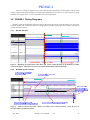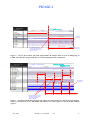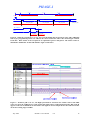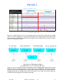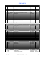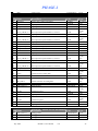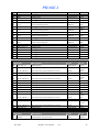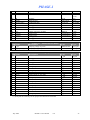
1
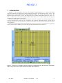
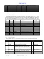
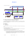
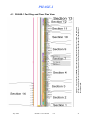
PHASE-1 User Manual PRELIMINARY VERSION A. Himmi, G. Bertolone, A. Brogna, W. Dulinski, C. Colledani, A. Dorokhov, Ch. Hu, F. Morel, I.Valin Institut de Recherches Subatomiques IN2P3-CNRS / ULP Strasbourg – France PHASE-1 Document history Version Date Description 1.0 Creation, based on Mimosa22 version July 2008 PHASE-1 chip Version Date 1.0 July 2008 Submitted 2008 Description Comments July AMS C35B4/Opto 640x640pixels, pitch Preliminary version 30µm, readout 160 MHz PHASE-1 User Manual v1.0 2 PHASE-1 1 2 Introduction .............................................................................................................................................. 4 Control Interface....................................................................................................................................... 5 2.1 JTAG Instruction Set....................................................................................................................... 5 2.2 JTAG Register Set........................................................................................................................... 5 2.2.1 Instruction Register .................................................................................................................... 6 2.2.2 DEV_ID Register ....................................................................................................................... 6 2.2.3 Bypass Register .......................................................................................................................... 6 2.2.4 Boundary Scan Register ............................................................................................................. 6 2.2.5 BIAS_DAC Register .................................................................................................................. 7 2.2.6 RO_MODE0 Register ................................................................................................................ 7 2.2.7 RO_MODE1 Register ................................................................................................................ 8 2.2.8 CONTROL_REG Register ......................................................................................................... 8 2.2.9 SEQUENCER_REG Register .................................................................................................... 9 2.2.10 DIS_DISCRI Register ......................................................................................................... 11 2.2.11 LINEPAT0_REG Register .................................................................................................. 11 2.2.12 LINEPAT1_REG Register .................................................................................................. 11 3 Running Phase1 ...................................................................................................................................... 12 3.1 After reset...................................................................................................................................... 12 3.2 Biasing Phase1 .............................................................................................................................. 12 3.3 Setting the Readout Configuration Registers ................................................................................ 13 3.4 Readout ......................................................................................................................................... 13 3.4.1 Signal protocol ......................................................................................................................... 13 3.4.2 Successive frames and resynchronisation................................................................................. 14 3.5 Analogue and digital Data Format ................................................................................................ 14 3.5.1 Normal mode data format......................................................................................................... 14 3.5.2 Test mode data format .............................................................................................................. 15 3.6 PHASE-1 Timing Diagrams.......................................................................................................... 16 3.6.1 Normal Readout ....................................................................................................................... 16 3.6.2 Readout synchronisation .......................................................................................................... 16 3.6.3 Main Signal Specifications....................................................................................................... 20 4 Pad Ring ................................................................................................................................................. 20 4.1 PHASE-1 Pad Ring and Floor Plan View ..................................................................................... 21 4.2 Pad List ......................................................................................................................................... 22 July 2008 PHASE-1 User Manual v1.0 3 PHASE-1 1 Introduction PHASE-1 is the intermediate version of the monolithic integrated detector to be used in the STAR experiment at RICH. The architecture is based on Mimosa22 with faster readout and larger matrix of pixels. The design process is Austria Mikrosysteme AMS-C35B4/OPTO which uses 4 metal- and 2 poly- layers. The thickness of the epitaxial layer is 14 µm. The design tools are provided by CMP (Cadence DFII, v5.1, IUS v 5.7, SoC v4.1 LDV v5) as well as the verification tools (Diva, Assura v3.17, Calibre v2007.02). The chip was submitted as Engineering Run on July 2008. The size of the chip is 19,52 mm x 20,93 mm, but the active area is 19.2mm x 19.2 mm and contains an array of 640 x 640 pixels with a pitch of 30 µm. An abstract view of the die is depicted in Figure 1 for the sake of clarity the picture is not in scale and does not reflect the real layout even if it shows all the main blocks and the chip architecture. Details how to program the internal functionalities of the chip are in Section 2, the information to operate the chip are in the Section 3 and the layout of the padring with chip bonding are in the Section 4. Figure 1 -- abstract view of the die, it does not reflect the real floorplan since the scale factor is altered for sake of clarity but it shows all the main blocks and the chip architecture July 2008 PHASE-1 User Manual v1.0 4 PHASE-1 2 Control Interface The control interface of PHASE-1 complies with Boundary Scan, JTAG, IEEE 1149.1 Rev1999 standard. It allows the access to the programmable internal registers. On power on, an internal reset Power-On –Reset is automatically generated for the control interface, the initial status of the Test Access Port (TAP) is Test-LogicReset and the ID register is selected. PHASE-1 has been designed in order to be fully tuneable via the control interface, nevertheless some voltages level might be forced from the external pads. 2.1 JTAG Instruction Set The Instruction Register of the JTAG controller is loaded with the code of the desired operation to perform or with the code of the desired data register to access. Instruction 5 Bit Code16 Selected Register EXTEST 01 BSR Notes JTAG mandatory instruction HIGHZ 02 BYPASS JTAG mandatory instruction INTEST 03 BSR JTAG mandatory instruction CLAMP 04 BYPASS JTAG mandatory instruction SAMPLE_PRELOA 05 BSR JTAG mandatory D instruction ID_CODE 0E DEV_ID register User instruction BIAS_GEN 0F BIAS_DAC User instruction PATTERNL0_REG 10 LINEPATL0_REG User instruction DIS_LATCH 11 DIS_DISCRI User instruction SEQ_REG 12 SEQUENCER_REG User instruction CTRL_REG 13 CONTROLER_REG User instruction PATTERNL1_REG 14 LINEPATL1_REG User instruction NU1 15 (1) Reserved, Not Used NU2 16 (1) Reserved, Not Used NU3 17 (1) Reserved, Not Used NU4 18 (1) Reserved, Not Used NU5 19 (1) Reserved, Not Used NU6 1A (1) Reserved, Not Used NU7 1B (1) Reserved, Not Used NU8 1C (1) Reserved, Not Used RO_MODE1 1D ReadOut Mode 1 User instruction RO_MODE0 1E ReadOut Mode 0 User instruction BYPASS 1F BYPASS JTAG mandatory instruction (1) Instruction codes implemented but not the corresponding registers. To be fixed in the next version. 2.2 JTAG Register Set JTAG registers are implemented with a Capture/Shift register and an Update register. JTAG standard imposes that the last significant bit of a register is downloaded/shifted first. Register Name Size Access Notes INSTRUCTION REG DEV_ID BYPASS 5 32 1 R/W R Only R Only Instruction Register July 2008 PHASE-1 User Manual v1.0 5 PHASE-1 BSR BIAS_DAC RO_MODE0 RO_MODE1 CONTROL_REG SEQUENCER_REG DIS_DISCRI LINEPATL0_REG LINEPATL1_REG NU1,NU2,…,NU8 2.2.1 10 120 8 8 40 128 640 640 640 0 R/W R/W R/W R/W R/W R/W R/W R/W R/W - Previous value shifted out during write Previous value shifted out during write Previous value shifted out during write Previous value shifted out during write Previous value shifted out during write Previous value shifted out during write Previous value shifted out during write Previous value shifted out during write Not implemented. For future use Instruction Register The Instruction register is a part of the Test Access Port Controller defined by the IEEE 1149.1 standard. The Instruction register of PHASE-1 is 5 bits long. On reset, it is set with the ID_CODE instruction. When it is read the 2 last significant bits are set with the markers specified by the standard, the remaining bits contain the current instruction. X 2.2.2 X X 1 0 DEV_ID Register The Device Identification register is a read-only 32-bit register. When selected by the ID_CODE instruction or after the fixed value is shifted via TDO, the JTAG serial output of the chip. PHASE-1 ID_CODE register value is 0x50483101. Bit # Bit Name Purpose Default value Code16 31-0 ID_CODE Device Identification register 50483101 2.2.3 ASCII ‘P’ ‘H’ ‘1’ <SOH> HEX 50 48 31 01 Bypass Register The Bypass register consists of a single bit scan register. It is selected when its code is loaded in the Instruction register, during some actions on the BSR and when the Instruction register contains an undefined instruction. 2.2.4 Boundary Scan Register The Boundary Scan Register, according with the Jtag instructions, tests and set the IO pads. The PHASE-1 BSR is 10 bits long and allows the test of the following input and outputs pads. Bit # Corresponding Pad Type Signal Notes 8 7 6 Input Input Input CkPLL CkCMOS ClkLvds PLL Clock CMOS Clock Resulting CMOS signal after LVDS Receiver CkPLL CkCMOS LVDS CkRdLn/CkRdLp July 2008 PHASE-1 User Manual v1.0 6 PHASE-1 5 START Input START Readout : Input synchronisation 4 3 2 1 0 SPEAK MK_CLK_A CLKA Tst2Pad Tst1Pad Input Ouput Ouput Ouput Ouput SPEAK MK_CLK_A CLKA Tst2Pad Tst1Pad Active Readout Marker & Clock Readout : Analogue Marker & Clock Readout Analogue Clock Readout Test Pad 2 Readout Test Pad 1 2.2.5 BIAS_DAC Register The BIAS_DAC register is 128 bit wide; it sets simultaneously the 16 DAC registers. As show bellow these 8-bit DACs set voltage and current bias. After reset the register is set to 0, a value which fixes the minimum power consumption of the circuit. The current values of the DACs are read while the new values are downloaded during the access to the register. An image of the value of each DAC can be measured on its corresponding test pad. Bit range DAC # DAC Internal Name DAC purpose Corresponding Test Pad 127-120 119-112 111-104 103-96 95-88 87-80 79-72 71-64 63-56 55-48 47-40 39-32 31-24 23-16 15-8 7-0 DAC15 DAC14 DAC13 DAC12 DAC11 DAC10 DAC9 DAC8 DAC7 DAC6 DAC5 DAC4 DAC3 DAC2 DAC1 DAC0 IKIMO IPIX IVTST2 IVTST1 IDIS2 IDIS1 IVDREF2 IVDREF1 IAnaBUF ILVDS ILVDSTX ID2PWRS ID1PWRS IBufBias IPwrSWBias ICLPDISC External circuit monitoring Pixel source follower bias Test Level, emulates a pixel output IDEM Discriminator bias 2 Discriminator bias 1 Discriminator Reference 2 Discriminator Reference 1 Analogue Buffer bias LVDS PAD bias LVDS PAD bias Discriminator bias 2 (mode low consp.) Discriminator bias 1 (mode low consp.) Ref&Tst Buffer bias Discriminator Power Pulse bias Discriminator Clamping bias VKIMO IPIX VTEST2 VTEST1 IDIS2 IDIS1 VDREF2 VDREF1 IAnaBUF ILVDS ILVDSTX 2.2.6 BUFBIAS PWRSWBIAS DISCLP RO_MODE0 Register The RO_MODE0 registers are 8 bits large; they allow the user to select specific digital mode of the chip. Bit # Bit Name Purpose Basic configuration value 7 En_TstBuf Enable the internal injection of VTEST 0 6 En_HalfMatrx Set the row shift register to 320 in place of 640 bits. 0 5 4 DisLVDS En_LineMarker 0 0 3 MODE_SPEAK 0 Marker signal active 2 Pattern_Only 0 Normal mode 1 En_ExtStart Disable LVDS and active clock CMOS. Add two rows at the end of matrix for a chip Readout: The LINEPAT_REG register is selected to emulate discriminators outputs. For analogue outputs, the 2 Test Levels, VTEST1 and VTEST2 are selected which emulate a pixel output. Select Marker signal or Readout Clock for digital and analogue data (MK_CLKA and MK_CLKD pads) Test Mode: Select LINEPAT_REG to emulate discriminators outputs Enable external START input synchronisation External injection of VTEST Normal mode, 640 row shift register selected LVDS selected Normal mode 0 Normal mode July 2008 PHASE-1 User Manual v1.0 7 PHASE-1 0 JTAG_Start (1) Enable Jtag START input synchronisation (2) 0 (1) The minimum wide of asynchronous external START is 2000 ns, and this signal is active at high level. (2) When En_ExtStart is disabled, it’s possible to generate internal START by accessing JTAG_Start bit. JTAG_Start signal is realized by three JTAG access: First step, this bit is set to 0, second step it is set to 1, and at last it is set to 0. 2.2.7 RO_MODE1 Register The RO_MODE1 registers are 8 bits large; they allow selecting specific analogue mode of the chip. Bit # Bit Name Purpose Basic configuration value 7 6 5 4 3 2 1 0 En_Pll En_AnaCol En_PixScan DisBufRef En_HS En_AOP_Disc En_Pulse_Discri En_TstDis Enable internal pll Enable analog output Enable scan pixel mode Disable the internal reference Enable High speed mode Enable the Power pulse Amplifier Enable the discri power pulse mode Enable the discri. test mode 0 0 0 0 0 0 0 0 2.2.8 Select Internal Buffer Select low speed mode Normal mode Normal mode Normal mode CONTROL_REG Register The CONTROL_REG registers are 40 bits large; they allow setting parameters of the readout controller. Bit # Bit Name Purpose Basic configuration value Code16 39-36 35-33 32-30 29-20 NU SelPad2 SelPad1 RowMkLast 0 0 0 027F 19-10 RowMkd 9-0 RowMka Reserved, Not Used Selection bit of Test2Pad Selection bit of Test1Pad Row number of the frame. It depends of readout mode. When the En_HalfMatrx mode is active, the value is 0x013F otherwise 0x027F. When the En_LineMarker mode is active, add two rows at the end of matrix. Selection parameter of row for digital marker (MK_Test_D) Selection parameter of row for analogue marker (MK_Test_A) 0 0 MK_Test_D signal MK_Test_A signal Normal mode, the number of row matrix is 640. Digital marker place is first row of matrix during the readout analogue marker place is first row of matrix during the readout The purpose of this array is to describe the internal signals which can be checked using 2 test pads (Tst1Pad and tst2Pad). The internal signals can be selected with SelPad1 and SelPad2 bits. SelPad1 Tst1Pad Purpose SelPad2 Tst2Pad Purpose 0 MK_Test_A Analogue marker is delayed of 500 ns respect to MK_A signal. This signal rises up at the beginning read phase and falls down at the end of Calib phase. It depends of RowMka selection 0 MK_Test_D Digital marker corresponding to last serialized digital data. It depends of RowMkd selection parameter. July 2008 PHASE-1 User Manual v1.0 8 PHASE-1 1 Mk_Rd 2 Mk_Calib 3 Ckdiv10 4 MK_A 5 Clp 6 Latch 7 CkDiv16 2.2.9 parameter. Analogue marker corresponding to Rd phase of readout pixel. It depends of RowMka selection parameter Analogue marker corresponding to Calib phase of readout pixel. It depends of RowMka selection parameter Main Clock is devised by 10 Analogue marker corresponding to readout pixel sequence. It depends of RowMka selection parameter. Set reference voltage for clamping Latch state of the discriminator Ckdiv10 is devised by 16 1 PwrOns Same signal as PwOn, but shifted of 16 main clock 2 PwOn Activate power supply for pixel 3 SlcRowInt 4 Clp Connect pixel output to common column Set reference voltage for clamping 5 RstDiode 6 Rd 7 Calib Set reference voltage for diode Sample before clamping Sample after clamping SEQUENCER_REG Register The SEQUENCER_REG registers are 128 bits large; this register contains all parameters to generate readout pixel and discriminator sequence. Bit # Bit Name Purpose Basic configuration value Code16 Signal Name 127-112 DataRdPix 7FFF Slct_Row_Int 111-96 DataRst1 0040 Rst 95-80 DataClp 01C0 Clamp 79-64 63-48 47-32 DataCalib DataRdDsc DataLatch 3C00 001C 6000 Calib Read Latch 31-0 DataPwrOn Connect pixel output to common column Set reference voltage for diode Set reference voltage for clamping Sample after clamping Sample before clamping Latch state of the discriminator Activate power supply for pixel July 2008 (1) 7FFFFFFF PHASE-1 User Manual v1.0 Pwr_On 9 PHASE-1 (1) Example: Generation of Latch Signal Msb • Lsb 15 14 13 12 11 10 9 8 7 6 5 4 3 2 1 0 0 1 1 0 0 0 0 0 0 0 0 0 0 0 0 0 Related timing with fCkdiv10=16 MHz (Read, Calib, Latch signals are used by the column readout circuitry). The Rst signal is not used for pixel. • This is readout sequence of the pixel and discriminator for 2 successive rows of matrix. In the wave form, the indexation of internal signal vectors is reversed compared with the Phase1 functional view (for example, the signal Pwr_On[639] corresponds to the row at the top of matrix). July 2008 PHASE-1 User Manual v1.0 10 PHASE-1 2.2.10 DIS_DISCRI Register The DIS_DISCRI register is 640 bits large. The purpose of this register is to disable the discriminator on a specific column if it is noisy, by gating Latch signal and setting the output discriminator at 0. The default value of the DIS_DISCRI register is 0; it means that all discriminators are activated. Setting a bit to 1 disables the corresponding discriminator. In Phase1, the DisableLatch<639> is on the left hand side while DisableLatch<0> is on the right hand side. 639 (Msb) DisableLatch<639> 0 (Lsb) DisableLatch<0> 2.2.11 LINEPAT0_REG Register The LINEPAT0_REG register is 640 bits large but only the first 630 are programmable. The purpose of this register is to emulate discriminators outputs rows in En_LineMarker and Pattern_Only modes. When Pattern_Only is active, the values stored in the pixel matrix are ignored and the value of LINEPAT0_REG is sent to the output. This is a test mode which emulates the (digital) pixel response with the contents programmed into the LINEPAT0_REG register in order to verify the digital processing. The pattern is alternated with the contents of the LINEPAT1_REG. In the En_LineMarker mode, it adds two rows at the end of matrix for a readout chip and the LINEPATL0_REG register is read to emulate the discriminators outputs of these two supplementary rows. This mode allows generating pattern marker in matrix data frame to detect chip readout desynchronization. Bit # Bit Name 639-630 Not used Purpose Reserved for the frame counter (read only) 629-0 LinePatL0Reg Emulate discriminators rows (1) This code is valid only after START (2) Example of pattern used in simulation. Basic configuration value Code16 200(1) 2AAAAA_AAAAAAAA_AAAAAAAA_AAAAAAAA(2) 2.2.12 LINEPAT1_REG Register The LINEPAT1_REG register is 640 bits large but only the first 630 are programmable. The purpose of this register is to emulate discriminators outputs rows in En_LineMarker and Pattern_Only modes. When Pattern_Only is active, the values stored in the pixel matrix are ignored and the value of LINEPAT0_REG is sent to the output. This is a test mode which emulates the (digital) pixel response with the contents programmed into the LINEPAT0_REG register in order to verify the digital processing. The pattern is alternated with the contents of the LINEPAT1_REG. In the En_LineMarker mode, it adds two rows at the end of matrix for a readout chip and the LINEPATL1_REG register is read to emulate the discriminators outputs of these two supplementary rows. This mode allows generating pattern marker in matrix data frame to detect chip readout desynchronization. Bit # Bit Name 639-630 Not used Purpose Reserved for the frame counter (read only) 629-0 LinePatL1Reg Emulate discriminators rows (1) This code is valid only after START (2) Example of pattern used in simulation. July 2008 Basic configuration value Code16 200(1) 155555_55555555_55555555_55555555(2) PHASE-1 User Manual v1.0 11 PHASE-1 3 Running Phase1 The following steps describe how to operate PHASE-1 3.1 After reset On RstB active low signal: • All BIAS registers are set to the default value, i.e. 0 • DIS_DISC is set to 0, i.e. all columns are selected • RO_MODE0 is set to 0 • RO_MODE1 is set to 0 • CONTROL_REG is set to 0 • SEQUENCER_REG is set to 0 • LINEPATL0_REG is set to 0 • LINEPATL1_REG is set to 0 • JTAG state machine is in the Test-Logic-Reset state • JTAG ID_CODE instruction is selected Then the bias register has to be loaded. The same for the RO_MODE0, RO_MODE1, CONTROL_REG, SEQUENCER_REG, LINEPATL0_REG, LINEPATL1_REG and DIS_DISC registers if the running conditions differ from defaults. Finally the readout can be performed either in normal mode or in test mode. 3.2 Biasing Phase1 The BIAS_DAC register has to be loaded before operating Phase1. The 16 DACs constituting this register are built with the same 8 bits DAC current generator which has a 1 µA resolution. Specific interfaces like current mirror for current sourcing or sinking and resistors for voltages, customise each bias output. The following table shows the downloaded codes which set the nominal bias. Internal DAC Name Simulation Resolu Range Code16 - DacInternal Output tion current-µA value Code10 Experimental Code16 - Code10 64-100 100 1V 10 mV 0 – 2.55 V 32-50 50 50 µA 1 µA 0 – 255 µA 71-118 118 1.18 V 10 mV 1 – 1.5 V 8C-118 118 1.18 V 250 µV -32 – 32 mV 20-32 32 5 µA 156 nA 0 – 255 µA 20-32 32 10 µA 312 nA 0 – 255 µA 71-118 118 1.18 V 10 mV 1 – 1.5 V 80-118 118 1.18 V 250 µV -32 – 32 mV(1) 32-50 50 500 µA 10 µA 0 – 255 µA 20-32 32 7 µA 218 nA 0 – 255 µA 28-40 40 40 µA 1 µA 0 – 255 µA A-10 10 100 nA 10 nA 0 – 255 µA A-10 10 100 nA 10 nA 0 – 255 µA A-10 10 10 µA 1 µA 0 – 255 µA A-10 10 10 µA 1 µA 0 – 255 µA 64-100 100 2.1 V 10 mV 1.2 – 3.2 V (1) Referenced with respect to IVDREF2. The threshold voltage of the discriminators is ΔVth = Vref1-Vref2 and the relationship is Vref1=Vref2+ΔVth IKIMO IPIX IVTST2 IVTST1 IDIS2 IDIS1 IVDREF2 IVDREF1 IAnaBUF ILVDS ILVDSTX ID2PWRS ID1PWRS IBufBias IPwrSWBias ICLPDISC July 2008 PHASE-1 User Manual v1.0 12 PHASE-1 Bias synthetic block diagram PIXELS SCAN IAnaBUF ... ... PAD Vref2 PAD Vref1 PAD Vtst2 PAD PAD Vtst1 IPIX VCLPDIS BUFFERS + - + - + - + - ... VTEST1 VTEST2 VDREF1 VDREF2 DISCLP 0 639 BUFBIAS DISCRIMINATORS + - POWER PULSE LVDS RECEIVER PWRSWBIAS LVDS DRIVER IDIS1 IDIS2 ID1PWRS ID2PWRS ILVDS ILVDSTX 3.3 Setting the Readout Configuration Registers If the desired operating mode does not correspond to the default one, set RO_MODE0, RO_MODE1, CONTROL_REG, SEQUENCER_REG, LINEPAT0_REG, LINEPAT1_REG registers following the §2.2.6, §2.2.7, §2.2.8, §2.2.9 and §2.2.11. 3.4 Readout 3.4.1 Signal protocol After JTAG registers have been loaded, the readout of PHASE-1 can be initialized with following signal protocol: • • • • Start readout clock (Master Clock 160 MHz); Initially set SPEAK signal to 0; Set to 1 the START signal for 2000 ns (minimum). During this step the internal reset is generated and then the clock dividers start to produce the clkdiv10 (16 MHz) and clkdiv (1 MHz); The readout controller starts at the first falling edge of clkdiv. Signal markers allow the readout monitoring and the data outputs (analogue and digital) sampling: CLKA and CLKD are running when readout controller starts. CLKA is a logic OR between Read and Calib signals and CLKD corresponds to 160 MHz (fast readout) or 40 MHz (slow readout); When SPEAK signal is active, markers of synchronisation for analogue and digital outputs are generated on MK_CLK_A and MK_CLK_D pads. July 2008 PHASE-1 User Manual v1.0 13 PHASE-1 3.4.2 Successive frames and resynchronisation Successive pixel frames are read meanwhile the readout clock is running. The frame resynchronisation can be performed at any time by setting up the “START” token again. SPEAK signal allows to generate markers signals which are used by DAQ. When SPEAK signal is set to 1 during the current frame an analogue marker appears on MK_SYNC_CLK_A pad and digital marker appears on MK_SYNC_CLK_D pad on next frame. In the MODE_SPEAK=’0’ (see Figure 9, Figure 10), the MK_SYNC_CLK_A marker corresponds to last row of the frame and the MK_SYNC_CLK_D marker corresponds to last bit frame. In the MODE_SPEAK=’1’, the MK_SYNC_CLK_A signal corresponds to a sampling clock for analogue outputs data (same as CLKA) which starts at the first row of frame. MK_SYNC_CLK_D signal corresponds to readout clock for digital data (same as CLKD) which starts at the first bit frame. When SPEAK signal is set to 0, MK_SYNC_CLK_A and MK_SYNC_CLK_D are set to 0. 3.5 Analogue and digital Data Format PHASE-1 uses the pads at the bottom edge for all its operations, whatever is collecting data from the pixels (using the pixels and the discriminators) or in test mode (reproducing at the outputs the pre-programmed patterns). All the digital signals to synchronize and programming the chip are necessary to operate successfully. Analog outputs located on the top edge of the chip are not used for the normal operations. The main purpose is to characterize the pixels or to check the dead pixels. Therefore measurements on these pads deal with normal pixel signals as well as test signals (but they still require the synchronization and the markers) and it is activated on demand by setting to 1 the En_AnaCol bit in the RO_MODE1 register. 3.5.1 Normal mode data format The digital part includes three blocks. One is JTAG controller interface which allows configure the internal registers used to readout chip. The second circuit generates the patterns necessary for addressing, resetting and double sampling of the signals in pixels in a column parallel way. The clock scans line by line at 1 MHz and latches the data in the output register which is divided in 4 parts each connected to one of the 4 main outputs. Figure 11 shows the internal structure of the output register and the serializer. There are 2 levels of multiplexing, first one runs at full speed of 160 MHz and the second one (4:1) which is used mainly for test purpose runs at lower speed of 40 MHz. Because of these additional multiplexing, the output data are scrambled. The Vref1 voltage is applied to the negative discriminator input during the read phase and the Vref2 voltage is applied during the Calib phase. The difference voltage Vref1 – Vref2 set the threshold of the discriminator. Voltages can be adjustable via 2 DACs or can be provided via 2 pads. When En_AnaCol bit is set to ‘1’ in the RO_MODE1 register, the rightmost 8 columns of pixels are connected to the analog outputs via a voltage follower and the signal is available on the pads. To start the analog test, the En_PixScan must be set to ‘1’ in the RO_MODE1. The scanning of the matrix now starts and stripes of 8 pixels are connected to the analog output. The analog test is performed considering a reduced size of the array (about 640 rows x 8 columns), therefore it takes 80 frame acquisitions to analyze the full matrix. Figure 1 shows how to do the analog characterization and which parts of the matrix are under test for each frame. The MK_CLKA is the synchronization marker for the analog outputs and it works like its digital homologue, see When En_AnaCol bit is set to ‘1’ it appears at the end of each frame, this signal is used to sample the analog July 2008 PHASE-1 User Manual v1.0 14 PHASE-1 8 bits 8 bits Frame N 8 bits Frame N +1 8 bits Frame N +2 8 bits Frame N +78 L0 Frame N +79 channel of the new frame on the next raising edge of CLKA. Further when the En_PixScan must be set to ‘1’, this marker appears at the end of the frame for each submatrix. L639 Figure 2 -- Analog characterization of the pixel: the matrix is divided in stripes of 8 columns and fully scanned at each frame, then swapped with the next block of 8 columns at right and so on until all the columns are analyzed. Data Ana Row 639 First Row add Vtest1 Vtest2 Data Ana Row 0 second Row add Vtest1 Vtest2 Figure 3 – Mode scan for analog output 3.5.2 Test mode data format This test readout mode allows obtain the transfer function of discriminator and calibrate the pixel readout chain. During the test mode the pixel matrix is not connected to discriminators and output analogue buffers. Instead of this, two test levels Vtst1, Vtst2 are connected to discriminator inputs to emulate pixel signal. July 2008 PHASE-1 User Manual v1.0 15 PHASE-1 The Vtst1 voltage is applied to the positive discriminator input during the Read phase and the Vtst2 voltage is applied during the Calib phase. Voltages can be adjustable via 2 DACs or can be provided via 2 pads. The difference voltage Vtst1 – Vtst2 corresponds to the pixel output signal. 3.6 PHASE-1 Timing Diagrams PHASE-1 needs an initialization step before starting the normal acquisition. After the master reset, the JTAG should be loaded with configuration and bias settings, then the START signal begins the automatic scanning ad readout of the pixel matrix. 3.6.1 Normal Readout Figure 4 – Beginning of readout mode. after Reset and JTAG settings the data are immediately available at the main outputs. Subsequent frames are automatically handled by the internal logic 3.6.2 Readout synchronisation Figure 5 – zoom on readout start, after a latency of 5 clkdiv cycles, readout of matrix starts, the zone on the right will be expanded for clarity July 2008 PHASE-1 User Manual v1.0 16 PHASE-1 Data Ana Row0 Data Ana Row1 Select low speed output Data Discri Row0 Select high speed output When EnaMux is rising, the serializer of data discriminators starts. Data are serialized on fall edge clock of CLKD Figure 6 – start of the serializer, the latch signal enables the outputs. Data are sent on falling edge of CLKD. It is visible the readout of the first row and the beginning of the serialization. En_LineMarker=1 MODE_SPEAK=0 Data Ana Row 639 Data Ana.Row 0 First Row add second Row add Vtest1 Vtest1 Vtest2 Last bit frame of serialization Vtest2 Last Row of frame During Read phase, Vtest1 is selected in analogue outputs, and during Calib phase, Vtest2 is selected Data Discri Row 639 LinePat0Reg LinePat1Reg Data Discri.Row0 Figure 7 – interframe timing diagram shows the ending of frame and first row digital data serialization, when En_LineMarker is set to 1 and MODE_SPEAK is set to 0. These options are set via the RO_MODE0 register. July 2008 PHASE-1 User Manual v1.0 17 PHASE-1 639 629 480 479 320 319 160 159 0 LINEPATL0Reg[629:0] or LINEPATL1Reg[629:0] Trame_id[9:0] START Frame n Frame n+1 B’10_0000_0000 B’01_0000_0000 Frame n+2 MK_LineMarker B’00_1000_0000 …… B’00_0000_0001 Trame_id[9:0] MK_LineMarker Latch Hx402AAA Hx401555 LinePat0Reg LinePat1Reg Figure 8 – When En_LineMarker is set to 1, the test of the digital data processing is active and 2 additional lines of pre-programmed patterns are added at the end of each frame. Then a new frame begins with the fresh data. Data format of the test-patterns is explained in §2.2.11 and §2.2.12. The frame counter is initialized to 0x200 after START and shifted to right at each frame. Figure 9 – When En_HS is set to 1, the High Speed mode is activated. The readout clock at 160 MHz comes out from the CLKD pad (or CLK_D internal signal) and a synchronization marker MK_CLK_D appears at the last serialized bit of each frame. This signal is used to sample the first bit of the new frame on the next raising edge of CLKD July 2008 PHASE-1 User Manual v1.0 18 PHASE-1 En_LineMarker=1 MODE_SPEAK=0 En_HS=0 Data Ana Row 0 Last bit frame of serialization first bit frame of serialization Figure 10 -- When En_HS is set to 0, the Low Speed mode is activated. The readout clock at 40 MHz comes out from the CLKD pad (or CLK_D internal signal) and a synchronization marker MK_CLK_D appears at the last serialized bit of each frame. This signal is used to sample the first bit of the new frame on the next raising edge of CLKD Figure 11 – There are 4 identical serializers in PHASE-1 one for each High Speed output. Here is the basic architecture of one of them which shows the 2 hierarchical levels of multiplexing. The first 40:1 generates the slow speed streams at 40 MHz (only for testing purpose) and the second one 4:1 assembles the data for the High Speed output at 160 MHz. Please observe the sequence at the output: this 2-levels architecture scrambles the data coming out from the high speed output . July 2008 PHASE-1 User Manual v1.0 19 PHASE-1 3.6.3 Main Signal Specifications INIT JTAG READOUT Analogue Driver Parameter Typical Value Notes RSTB Pulse Width TCK Frequency TMS Setup/Hold Time TDI Setup/Hold Time CKRD Frequency CKRD Duty Cycle START Setup/Hold Time SPEAK Setup/Hold Time Input Dynamic range Rise time Fall time Bandwidth Output Current Range >1 μS 10 MHz ~10 nS ~10 nS Up to 100 MHz 50% 5 ns 5 ns Active Low, Asynchronous Power on Reset Boundary Scan Clock Boundary Scan Control Signal Boundary Scan Serial Data In Readout Clock LVDS signal Chip Initialisation, CMOS signal. Active Readout Marker & Clock 4 Pad Ring The pad ring of PHASE-1 is build with • Pads full custom designed for some of the analogue signals and power supplies • Pads from the AMS library for the digital signals and power supplies The pad ring is split in 8 functional independent parts CMOS JTAG and Test purpose pads LVDS Read Out Drivers Digital outputs Read Out Analogue Outputs Bias Test Analogue and Digital Power supplies Test structure 1 Test structure 2 Each part has its own supply pads. July 2008 PHASE-1 User Manual v1.0 20 Figure 12 – The pad layout of PHASE-1. Only the top edge and the bottom edge are visible. The pads used for the test with a probe station are also drawn but not named because they reproduce the functionality of the adjacent pad. PHASE-1 4.1 PHASE-1 Pad Ring and Floor Plan View July 2008 PHASE-1 User Manual v1.0 21 PHASE-1 4.2 Pad List Pad Name 1 2 3 4 5 6 7 TEMP gnda! gnda!_Prob (*) v_clp! v_clp!_Prob (*) vdda!_Prob (*) vdda! Pad Name 8 9 10 --11 --12 --- Section 1 – Temperature sensor and Analog bias for pixels Description Cell temperature sensor analog ground analog ground clamping voltage for pixels clamping voltage for pixels analog power analog power DIRECTPAD AGND3ALLP AGND3ALLP DIRECTPAD DIRECTPAD AVDD3ALLP AVDD3ALLP Section 2 – JTAG control and Digital Output Channel 3 Description Cell vdd!_Prob (*) vdd! TCK digital power digital power JTAG clock TDI JTAG data input TMS JTAG mode state VDD3ALLP VDD3ALLP ICCK2P ProbePad ICUP ProbePad ICUP ProbePad 13 --14 15 16 TDO JTAG data output gnd!_Prob (*) gnd! gnd!_Prob (*) digital ground digital ground digital ground BT4P ProbePad GND3ALLP GND3ALLP GND3ALLP 17 18 OUT3_CMOS<3> gnd! data output slow speed channel 3, stream 3 digital ground BU4P GND3ALLP 19 20 --21 22 --23 OUT3_CMOS<2> gnd! data output slow speed channel 3, stream 2 digital ground OUT_LVDSp<3> OUT_LVDSn<3> data output fast speed, channel 3 data output fast speed, channel 3 vdd! digital power BU4P GND3ALLP probePad LVDS-TX LVDS-TX ProbePad VDD3ALLP 24 25 OUT3_CMOS<1> vdd! data output slow speed channel 3, stream 1 digital power BU4P VDD3ALLP 26 27 OUT3_CMOS<0> vdd!_Prob (*) data output slow speed channel 3, stream 0 digital power BU4P VDD3ALLP Type direct pad power power power power power power Type power power DI-clockin DI-pullup DI-pullup DO 3-state, 4mA probe power power power DO 3-state, 4mA power DO 3-state, 4mA power probe DO LVDS DO LVDS probe power DO 3-state, 4mA power DO 3-state, 4mA power Section 3 – Analog bias and DACs July 2008 PHASE-1 User Manual v1.0 22 PHASE-1 Pad Name Description Cell Type 28 29 30 31 32 33 34 35 --36 37 38 gnda!_Prob (*) gnda! vdda! vdda! vdda! vdda!_Prob (*) gnda! Itest analog ground analog ground analog power analog power analog power analog power analog ground gnda! VCLPDIS gnda! analog ground discriminator clamping, external injection analog ground AGND3ALLP AGND3ALLP AVDD3ALLP AVDD3ALLP AVDD3ALLP AVDD3ALLP AGND3ALLP APRIOP probePad AGND3ALLP DIRECTPAD AGND3ALLP 39 40 41 42 43 44 45 46 47 48 VKIMO gnda! VCLPDIS gnda! vdda!_Prob (*) vdda! vdda! vdda! gnda! gnda!_Prob (*) circuit monitoring analog ground discriminator clamping, external injection analog ground analog power analog power analog power analog power analog ground analog ground APRIOP AGND3ALLP DIRECTPAD AGND3ALLP AVDD3ALLP AVDD3ALLP AVDD3ALLP AVDD3ALLP AGND3ALLP AGND3ALLP Power Power Power Power Power Power Power Power Probe Power direct pad Power AIO 0 Ohm Power direct pad Power Power Power Power Power Power Power Pad Name 49 --50 Section 4 – Synchronization and Digital Output Channel 2 Description Cell SPEAK activate readout marker and clock vdd!_Prob (*) digital power 51 --52 --53 54 --55 56 START synchronize the outputs vdd! digital power MK_CLKD_p MK_CLKD_n marker and clock for digital data marker and clock for digital data gnd! gnd!_Prob (*) digital ground digital ground ICPD probePad VDD3ALLP probePad LVDS-TX LVDS-TX probePad GND3ALLP GND3ALLP 57 58 OUT2_CMOS<3> gnd! data output slow speed channel 2, stream 3 digital ground BU4P GND3ALLP 59 60 --61 62 OUT2_CMOS<2> gnd! data output slow speed channel 2, stream 2 digital ground OUT_LVDSp<2> OUT_LVDSn<2> data output fast speed, channel 2 data output fast speed, channel 2 BU4P GND3ALLP probePad LVDS-TX LVDS-TX July 2008 PHASE-1 User Manual ICPD probePad VDD3ALLP v1.0 Type DIpulldown Probe Power DIpulldown Probe Power Probe DO LVDS DO LVDS Probe Power power DO 3-state, 4mA power DO 3-state, 4mA power probe DO LVDS DO LVDS 23 PHASE-1 --63 vdd! digital power probePad VDD3ALLP digital ground ISUP probePad GND3ALLP probe power DO 3-state, 4mA power DO 3-state, 4mA power power probe DO LVDS DO LVDS probe power DI-pullup, schmitt probe power 64 65 OUT2_CMOS<1> vdd! data output slow speed channel 2, stream 1 digital power BU4P VDD3ALLP 66 67 68 --69 70 --71 OUT2_CMOS<0> vdd!_Prob (*) vdd! data output slow speed channel 2, stream 0 digital power digital power CLKD_p CLKD_n readout clock for digital data readout clock for digital data BU4P VDD3ALLP VDD3ALLP probePad LVDS-TX LVDS-TX probePad gnd! digital ground 72 --73 RSTB asynchronous reset, active low gnd!_Prob (*) Pad Name Section 5 – Analog bias for pixels Description Cell Type 74 75 76 analog ground clamping voltage for pixels analog power AGND3ALLP DIRECTPAD AVDD3ALLP power direct pad power Section 6 – Master clock (LVDS) Description Cell Type GND3ALLP GND3ALLP probePad LVDS-RX LVDS-RX probePad VDD3ALLP VDD3ALLP power power probe DI LVDS DI LVDS probe power power gnda! v_clp! vdda! Pad Name 77 78 --79 80 --81 82 gnd!_Prob (*) gnd! digital ground digital ground CKR_p CKR_n master clock, LVDS compatible master clock, LVDS compatible vdd! vdd!_Prob (*) digital power digital power Pad Name Section 7 – Master clock (PLL synthesizer) Description Cell Type 83 84 85 86 87 88 digital power digital ground master clock, low frequency analog ground analog power analog ground VDD3ALLP GND3ALLP ICCK2P AGND3ALLP AVDD3ALLP AGND3ALLP power power DI clockin power power power Pad Name Section 8 – Analog bias for pixels Description Cell Type 89 90 analog ground clamping voltage for pixels AGND3ALLP DIRECTPAD power direct pad VDDD GNDD REFCLK GNDA VDDA GNDV gnda! v_clp! July 2008 PHASE-1 User Manual v1.0 24 PHASE-1 91 vdda! Pad Name analog power AVDD3ALLP Section 9 –Digital Output Channel 1 and Readout clock Description Cell 92 --93 94 CKCMOS master clock, CMOS compatible vdd! gnd!_Prob (*) digital power digital ground ICCK2P probePad VDD3ALLP GND3ALLP 95 96 OUT1_CMOS<3> gnd! data output slow speed channel 1, stream 3 digital ground BU4P GND3ALLP 97 98 OUT1_CMOS<2> gnd! data output slow speed channel 1, stream 2 digital ground 99 100 --101 OUT_LVDSp<1> OUT_LVDSn<1> data output fast speed, channel 1 data output fast speed, channel 1 vdd! digital power BU4P GND3ALLP probePad LVDS-TX LVDS-TX ProbePad VDD3ALLP 102 103 OUT1_CMOS<1> vdd! data output slow speed channel 1, stream 1 digital power BU4P VDD3ALLP 104 105 OUT1_CMOS<0> vdd!_Prob (*) data output slow speed channel 1, stream 0 digital power BU4P VDD3ALLP 106 --- CLKA readout clock for analog data BT4P probePad 107 --108 MK_CLKA marker and clock for analog data gnda!_Prob (*) digital ground BT4P probePad GND3ALLP 109 --110 tst1pad readout test pad 1 vdd!_Prob (*) digital power 111 --112 tst2pad readout test pad 2 gnd! digital ground BT2P probePad VDD3ALLP BT2P probePad GND3ALLP power Type DI clockin probe power power DO 3-state, 4mA power DO 3-state, 4mA power probe DO LVDS DO LVDS probe power DO 3-state, 4mA power DO 3-state, 4mA power DO 3-state, 4mA probe DO 3-state, 4mA probe power DO 3-state, 2mA probe power DO 3-state, 2mA probe power Pad Name Section 10 – Analog test for discriminator Description Cell Type 113 114 115 analog ground analog ground analog power power power power gnda!_Prob (*) gnda! vdda! July 2008 PHASE-1 User Manual AGND3ALLP AGND3ALLP AVDD3ALLP v1.0 25 PHASE-1 116 117 118 119 120 vdda! vdda! vdda! vdda!_Prob (*) gnda! analog power analog power analog power analog power analog ground AVDD3ALLP AVDD3ALLP AVDD3ALLP AVDD3ALLP AGND3ALLP 121 122 Vtst1 gnda! vtest1, external injection analog ground APRIOP AGND3ALLP 123 124 Vtst2 gnda! vtest2, external injection analog ground APRIOP AGND3ALLP 125 126 Vref2 gnda! vref2, external injection analog ground APRIOP AGND3ALLP 127 128 129 130 131 132 133 134 Vref1 gnda! vdda!_Prob (*) vdda! vdda! vdda! gnda! gnda!_Prob (*) vref2, external injection analog ground analog power analog power analog power analog power analog ground analog ground APRIOP AGND3ALLP AVDD3ALLP AVDD3ALLP AVDD3ALLP AVDD3ALLP AGND3ALLP AGND3ALLP power power power power power AIO 0 Ohm power AIO 0 Ohm power AIO 0 Ohm power AIO 0 Ohm power power power power power power power Pad Name Section 11 – Digital Output Channel 0 Description Cell 135 gnd!_Prob (*) digital ground GND3ALLP 136 137 OUT0_CMOS<3> gnd! data output slow speed channel 0, stream 3 digital ground BU4P GND3ALLP 138 139 --140 141 --142 OUT0_CMOS<2> gnd! data output slow speed channel 0, stream 2 digital ground OUT_LVDSp<0> OUT_LVDSn<0> data output fast speed, channel 0 data output fast speed, channel 0 vdd! digital power BU4P GND3ALLP probePad LVDS-TX LVDS-TX ProbePad VDD3ALLP 143 144 OUT0_CMOS<1> vdd! data output slow speed channel 0, stream 1 digital power BU4P VDD3ALLP 145 146 OUT0_CMOS<0> vdd!_Prob (*) data output slow speed channel 0, stream 0 digital power BU4P VDD3ALLP Section 12 – Test: PLL synthesizer Description Cell Type ISUP DI-pullup, schmitt Pad Name 147 RESET July 2008 asynchronous reset, active low PHASE-1 User Manual v1.0 Type power DO 3-state, 4mA power DO 3-state, 4mA power probe DO LVDS DO LVDS probe power DO 3-state, 4mA power DO 3-state, 4mA power 26 PHASE-1 148 149 VDDD REFCLK digital power master clock, CMOS compatible VDD3ALLP ICCK2P 150 151 152 153 154 155 FB GNDD OUTCLOCKp OUTCLOCKn VDDAI GNDA feedback digital ground synthesized clock synthesized clock analog power analog ground BU4P GND3ALLP LVDS-TX LVDS-TX AVDD3ALLP AGND3ALLP 156 157 158 159 160 CTL VDDAO VDDVO VDDVI GNDV voltage control for oscillator analog power analog power analog power analog ground APRIOP AVDD3ALLP AVDD3ALLP AVDD3ALLP AGND3ALLP power DI clockin DO 3-state, 4mA power DO LVDS DO LVDS power power AIO 0 Ohm power power power power Pad Name Section 13 – Analog bias for pixels Description Cell Type 161 162 clamping voltage for pixels clamping voltage for pixels DIRECTPAD DIRECTPAD direct pad direct pad v_clp! v_clp!_Prob (*) Pad Name --163 --164 --165 --166 --167 --168 --169 --170 --171 --172 Section 14 – Test : Analog outputs from the matrix Description Cell gnd!_test analog ground vdda!_test analog power Out<0> analog output<0> test mode Out<1> analog output<1> test mode Out<2> analog output<2> test mode Out<3> analog output<3> test mode Out<4> analog output<4> test mode Out<5> analog output<5> test mode Out<6> analog output<6> test mode Out<7> analog output<7> test mode g_pad g_pad g_pad g_pad g_pad g_pad g_pad g_pad g_pad g_pad g_pad g_pad g_pad g_pad g_pad g_pad g_pad g_pad g_pad g_pad Type test pad test pad test pad test pad test pad test pad test pad test pad test pad test pad test pad test pad test pad test pad test pad test pad test pad test pad test pad test pad (*) Probe pads are used only for test purpose and should not be bonded July 2008 PHASE-1 User Manual v1.0 27