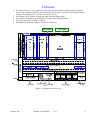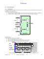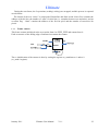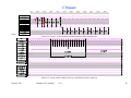
1
Ultimate User Manual A. Himmi, G. Doziere, G. Bertolone, W. Dulinski, C. Colledani, A. Dorokhov, Ch. Hu, F. Morel, H. Pham, I.Valin, J Wang Institut Pluridisciplinaire Hubert Curien IN2P3-CNRS / UdS Strasbourg – France Y. Degerli, F. Guilloux CEA Saclay DAPNIA/SEDI January 2011 Ultimate User Manual V.1.1 1 Document history Version Date 1.0 1.1 December 2010 January 2011 Ultimate chip Version Date 1.0 Description Based on Mimosa-26 Version Description Comments Submitted January 11 AMS 035 Opto Version, 928 x 960 pixels January 2011 Ultimate User Manual V.1.1 2 Ultimate 1 Suze and main sequencer ................................................................................................................. 5 1.1 General description of STAR CMOS pixel sensor .................................................................. 5 1.2 Architecture description ........................................................................................................... 5 1.3 Ultimate main synoptic ............................................................................................................ 7 1.4 Synoptic of SUZE .................................................................................................................... 8 1.5 SPARSE DATA SCAN (SDS) ................................................................................................ 8 1.5.1 Introduction ...................................................................................................................... 8 1.5.2 One block description....................................................................................................... 9 1.5.3 Timing diagram for control signals................................................................................ 10 1.5.4 Algorithm sparse data scan (SDS) description............................................................... 11 1.5.5 Synoptic.......................................................................................................................... 12 1.5.6 Coding ............................................................................................................................ 13 1.6 States multiplexer................................................................................................................... 14 1.6.1 Introduction .................................................................................................................... 14 1.6.2 Coding ............................................................................................................................ 15 1.6.3 Module 6 x 8 9 and module 6 x 7 9 ..................................................................... 15 1.6.4 Module 2 x 9 9 .......................................................................................................... 18 1.7 Memory management............................................................................................................. 19 1.7.1 Memory control + multiplexer test + RAM ................................................................... 19 1.7.1.1 Introduction ................................................................................................................ 19 1.7.1.2 Top view diagram....................................................................................................... 19 1.7.1.3 Working mode............................................................................................................ 21 1.7.2 Frame counter................................................................................................................. 22 1.7.3 Serializer and data format .............................................................................................. 23 2 Control Interface ............................................................................................................................ 24 2.1 Introduction ............................................................................................................................ 24 2.2 JTAG Instruction Set.............................................................................................................. 24 2.3 JTAG Register Set.................................................................................................................. 25 2.4 Instruction Register ................................................................................................................ 26 2.4.1 DEV_ID Register ........................................................................................................... 26 2.4.2 Boundary Scan Register (BSR)...................................................................................... 26 2.5 THE BIAS_GEN Register ..................................................................................................... 27 2.6 patt_line0 register................................................................................................................... 29 2.7 dis_disc register...................................................................................................................... 29 2.8 pix_seq Register ..................................................................................................................... 30 2.9 Monitoring1 register............................................................................................................... 30 2.10 patt_line1 Register.................................................................................................................. 31 2.11 suze_seq register .................................................................................................................... 32 2.12 header_trailer register............................................................................................................. 33 2.13 Monitor 2 Register ................................................................................................................. 34 2.14 RO_MODE4 Register ............................................................................................................ 36 2.15 RO_MODE3 Register ............................................................................................................ 36 2.16 RO_MODE2 Register ............................................................................................................ 37 2.17 RO_MODE1 Register ............................................................................................................ 37 2.18 RO_MODE0 Register ............................................................................................................ 38 2.19 BYPASS Register .................................................................................................................. 38 3 Running Ultimate ........................................................................................................................... 39 3.1 Reset initialization.................................................................................................................. 39 January 2011 Ultimate User Manual V.1.1 3 Ultimate 3.1.1 Introduction .................................................................................................................... 39 3.1.2 Sequence......................................................................................................................... 39 3.2 After reset............................................................................................................................... 39 3.3 Setting the bias_gen register .................................................................................................. 40 3.4 Analogue and digital Data Format ......................................................................................... 42 3.4.1 Main Introduction........................................................................................................... 42 3.4.2 Normal mode data format .............................................................................................. 42 3.4.2.1 Introduction ................................................................................................................ 42 3.4.2.2 The Clock ................................................................................................................... 43 3.4.2.3 Marker ........................................................................................................................ 43 3.4.2.4 Header trailer.............................................................................................................. 43 3.4.2.5 Frame counter............................................................................................................. 43 3.4.2.6 Data Length ................................................................................................................ 43 3.4.2.7 Useful data (States/Line, State) .................................................................................. 43 3.4.3 Test mode ....................................................................................................................... 48 3.4.3.1 Analogue outputs, Normal pixel signal...................................................................... 48 3.4.4 Transfer function of discriminator and pixel digital readout calibration ....................... 50 3.4.4.1 Introduction ................................................................................................................ 50 3.4.4.2 Transfer function of discriminator: ............................................................................ 50 3.4.4.3 Pixel digital readout calibration: ................................................................................ 50 3.4.4.4 Synoptic...................................................................................................................... 50 3.4.4.5 Transfer function of discriminator and pixel digital readout calibration ................... 51 3.4.4.6 Timing diagram .......................................................................................................... 51 3.4.5 SUZE multiplexer test.................................................................................................... 53 3.4.5.1 Introduction ................................................................................................................ 53 3.4.5.2 Configuration test....................................................................................................... 53 3.4.5.3 Synoptic...................................................................................................................... 53 3.4.5.4 MUX scanning word description ............................................................................... 54 3.5 Main sequencer ...................................................................................................................... 55 3.5.1 Introduction .................................................................................................................... 55 3.5.2 Main phases for ultimate ................................................................................................ 55 3.5.3 Synchronization for stop and re-start readout ................................................................ 56 3.5.4 Chronograms for a the first frame readout ..................................................................... 57 3.5.5 Line synchronization for pixel and discriminator .......................................................... 60 3.5.6 Line synchronization for suze ........................................................................................ 60 3.5.7 Pipeline of the readout chain.......................................................................................... 61 3.6 Pixel and analog core sequencer ............................................................................................ 61 3.6.1 Pixel and discriminator read out sequence synchronization .......................................... 61 3.6.2 Disable discriminator output sequence .......................................................................... 67 3.6.3 Analog discriminators sequence test .............................................................................. 67 3.7 Main Signal Specifications..................................................................................................... 68 3.8 Pad Ring ................................................................................................................................. 69 3.9 Pad List................................................................................................................................... 70 4 Glossary, abbreviations and acronyms tables. .............................................................................. 77 January 2011 Ultimate User Manual V.1.1 4 Ultimate 1 1.1 Suze and main sequencer General description of STAR CMOS pixel sensor Ultimate is the final sensor chip for the upgrade of STAR inner layer of the vertex detector. Its architecture integrates main function of Mimosa26 (Monolithic Active Pixel Sensor (MAPS) with fast binary readout) and including a zero suppression logic. The sensor consists of a matrix composed by 928 (rows) x 960 (columns) pixels of 20.7 µm pitch for a size of the chip of 20.22 mm x 22.71 mm. The design process Austria Micro System AMS-C35B4/OPTO uses 4 metal- and 2 poly- layers. The thickness of the epitaxial layer stretches out up to 15 µm in Hi-Resistivity substrate (400 Ohm.cm). The design tools follow the CADENCE DFII 5.1 with DIVA, ASSURA, CALIBRE rules. The chip has been submitted in an Engineering Run via CMP on 20 January 2011 In the STAR vertex detector, the hit rate is evaluated at 2.4 x 10⁵ hits/s/cm². The design of the sensor is driven by the high readout frequency in order to keep the track multiplicity per frame at a low level. It is done by read out pixel columns in parallel, row by row. The chip readout time is 185.6 µs. Each pixel includes an amplification and Correlated Double Sampling (CDS) and each end of column is equipped with a discriminator. The threshold of the discriminator is programmable by slow control. After analogue to digital conversion, digital signals pass through the zero suppression block. The digital signals are processed in parallel on 15 banks, then arranged and stored in a memory row by row. Two memories banks have been implemented in the sensor to perform read and write operations simultaneously (see §Memory management). At each frame, the circuit sends a specific marker to initialize the formatted readout and inside the data, some specifics words give also synchronization markers to begin and start the readout. The chip offers the choice of the output bit rate of the communication. 160 or 80 Mbits /second. The configuration by JTAG protocol allows the programming of the test, the masking and the control of the discriminator. A self in built test is included in the chip for debug of all main digital parts. (see Figure 1 : Ultimate functional view). 1.2 Architecture description The core digital includes two main parts called ult_manager and suze. The first part ult_manager contains: the jtag controller treating the configuration registers for the matrix readout (both analog and digital part), for testability the command of the possibility to disable the discriminators, the pixel sequence read-out block managing the sampling of the pixel, the matrix analog readout sequence, the mode selection for suze input, the user choices the readout of the analog matrix, the virtual matrix generated by the repetition of 2 lines pattern given, or the synchronization test frame. The second part suze contains: the sparse data scan (sds) extracting by block up to 6 hits (for the line up to 6 x15), the second stage the mux6x15 to 9 retains 9 states from the previous one, January 2011 Ultimate User Manual V.1.1 5 Ultimate the main sequencer a key component of the chip generates all the synchronization signals for the line the operations inside the line and for the whole frame. It produces also the line address counter. In running mode, it reaches maximum 928 lines. the boundary scan chain for testing the main input and output pads, the memory management sequencing the writing and reading operation, the ram (4 memories of 2048 x 16 bits) additional test structure acting as a probe for each block, Figure 1 : Ultimate functional view January 2011 Ultimate User Manual V.1.1 6 Ultimate 1.3 Ultimate main synoptic The following synoptic shows the implementation of SUZE into Ultimate. Figure 2: top view implementation of SUZE in ULTIMATE This digital part manages sequentially each line for the whole frame composed of 928 lines x 960 columns. The main sequencer gives to the structure the address of lines and all synchronizations and controls signals. A JTAG controller brings the configuration information. (Table of configurations registers) A test structure simulates a matrix of pixel in order to check the functions of SUZE. January 2011 Ultimate User Manual V.1.1 7 Ultimate 1.4 Synoptic of SUZE This digital part includes 3 main parts: The Sparse Data Scan (SDS), The multiplexer, And the memory management. 1 status + 6 states 960 bits 9 states & status Tests PADS 1 status + 6 states Figure 3: SUZE block diagram 1.5 1.5.1 SPARSE DATA SCAN (SDS) Introduction 8 7 6 5 895 -832 831 – 768 767 – 704 703 – 640 639 – 960 575 – 512 511 – 448 447 – 384 383 – 320 4 3 2 1 0 63-0 9 127- 64 10 191 -128 11 255 -192 12 319 -256 13 Pixels per block Block 14 959 – 896 Based on a sparse data scan algorithm to find hit pixels (discriminator output = “1”), this module Sparse Data Scan (SDS) receives a line constituted of 960 pixels (959 to 0) divided in 15 blocks of 64 pixels. Up to 4 contiguous pixel signals above Vthreshold of the discriminator will be encoded in a 2 bits state word following the address of the 1st pixel Each block extracts of the 64 pixels bus: 1 status group, 6 states, (column addresses + encoded state) 1 overlapping. These 15 blocks works in parallel and give 6 x 15 states to the next stage. January 2011 Ultimate User Manual V.1.1 8 Ultimate One block description The next figure shows the different steps of the sparse data scan for one block. 1.5.2 Figure 1: Schematic view of sparse data scan for one block The algorithm proceeds through four consecutive steps, summarized below: In the first step, the data inputs for the process are extracted from 64 discriminators; The second step consists in encoding groups of hit pixels. This logic provides Enable bits and Code bits for each column composing a bank. The Enable bit is set to 1 for the first hit pixel in a group. The number of Enable bits set to 1 characterizes the state; January 2011 Ultimate User Manual V.1.1 9 Ultimate The third step selects the “states”; each “state” is selected successively by a sparse data scan. It uses a chain of alternated NAND and NOR gates for the priority management during the sparse-scan. The generation of “states” requires several instructions. The number of “states” (N) in a bank is related to M “states” in a row. The algorithm manages up to N = 6 instructions or “states” in a bank; At each instruction, the column address of the “state” is decoded. The last digital step stores the N “states” and generates “status” information indicating the number of “states” per bank. Each bank has its own address encoded in 5 bits. Timing diagram for control signals These inputs signal are given by the main sequencer 1.5.3 Figure 4: Synchronization signals for SDS timing diagram January 2011 Ultimate User Manual V.1.1 10 1.5.4 Algorithm sparse data scan (SDS) description C63 C0 0 0 0 0 0 1 1 1 1 1 0 0 0 0 0 0 0 0 0 1 1 1 0 0 0 latch C0 E0 ckrdpix rstpix State1 64 Discriminators at bottom of bank (Read row by row ) Discriminators Row C63 …… Coding Coding (Data compression) E1 …… E63 Rd1 …… Pixel in group State selection This is the sequence used to decode column address of first hit pixel in group, it’s corresponding to read enable bit which is set to ‘1’. The number of instruction is limited at 6 Col. address Bank Results …. 8b H I T 5 5b 4b A D R Bank Adr. 8b 8b H I T 0 State 5 January 2011 Each state is composed of 6 bits Column address plus 2 bits code State 0 State: Data 8 bits Storing of N states by bank and generating status register 1er Inst 2 Inst 3 Inst … 6 Inst Rd63 Column Address decoder (64 to 6) ckmemlatch Enable bit is set to 1 for first hit Code: 2 bits C1 Selection of column address of first hit pixel in group (Sparse Data Scan algorithm) Rd0 State3 State2 By Colum n: Enable : 1 bit Maximum 6 States registers of 8 bits Bank address register of 5 bits Status register of 3 bits (number of states by bank) Sm STATUS[2:0] STATUS[2:0] Ovf Ultimate User Manual V.1.1 11 1.5.5 Synoptic Figure 5: SDS block diagram January 2011 Ultimate User Manual V.1.1 12 Ultimate Coding 1.5.6 The following table shows the format of the result for one block. State 0 0 1 2 0 1 2 Status block 3 4 0 1 coding State 3 5 6 0 7 State 1 8 State 2 9 10 11 12 13 14 15 16 17 18 19 20 21 22 23 24 25 26 1 2 3 4 5 0 1 0 1 2 3 4 5 0 1 0 1 2 3 4 5 Column address coding Column address coding Column address State 4 State 5 new_bit210j 27 28 29 30 31 32 33 34 35 36 37 38 39 40 41 42 43 44 45 46 47 48 49 50 51 52 53 0 1 0 1 2 3 4 5 0 1 0 1 2 3 4 5 0 1 0 1 2 3 4 5 0 1 2 coding Column address coding Column address coding Column address Overlapping Figure 6: format of the SDS results For the whole line, we have 15 x (1 status blocks and 6 states). January 2011 Ultimate User Manual V.1.1 13 Ultimate 1.6 States multiplexer Introduction The states multiplexer reads out the outcomes of the 15 banks x 6 states and keep up maximum 9 states from the previous stage SDS. Three objects constitute this block: 2 identical modules (Mux 6x8 9) which extract each one 9 states and 1 status for an half line 1 module (Mux 2 x 9 9) which retains 9 states and a status from these 2 modules 1.6.1 Figure 7: Multiplexor top view Sample signals This synchronous module uses 3 signals The first one initiate the process: rstline The second one samples the selection of the hit kept: ckrdpix The third one en_fsm_mux signal latches the record states. Figure 8: Synchronization signals for MUX 6 x 8 9 , MUX 6 x 7 9top view January 2011 Ultimate User Manual V.1.1 14 Ultimate Figure 9: Module 6 x 9 9 top view Coding The following table shows the format of the result for the line given to the memory management. 1.6.2 State 0 3 4 5 6 7 8 State 1 9 10 11 12 13 14 3 4 5 6 7 8 9 A B C D E 3 0 1 2 3 4 5 6 7 8 9 Row 15 16 17 18 19 20 21 22 28 29 30 31 F 0 1 2 3 4 5 6 7 8 9 A B C 15 0 1 0 1 2 3 4 5 6 7 8 9 OVF Coding Column D E F State 2 35 36 37 38 39 40 23 24 25 26 27 State 3 41 42 43 44 45 46 47 48 49 50 51 52 53 54 60 61 62 63 3 4 5 6 7 8 9 A B C 1 2 3 4 5 6 7 8 9 Column D E F 0 1 2 3 4 5 6 7 8 9 A B C 0 1 0 1 2 3 4 5 6 7 8 9 Column Coding D E F 76 77 78 79 80 92 93 94 95 3 4 5 6 7 8 9 A B C 1 2 3 4 5 6 7 8 9 Column D E F 0 1 2 3 4 5 6 7 8 9 A B C 0 1 0 1 2 3 4 5 6 7 8 9 Column Coding D E F State 4 67 68 69 70 71 72 55 56 57 58 59 State 5 73 74 75 81 82 83 84 85 86 State 6 87 88 89 90 91 State 7 99 100 101 102 103 104 105 106 107 108 109 110 111 112 113 114 115 116 117 118 119 120 121 122 123 124 125 126 127 3 4 5 6 7 8 9 A B C 1 2 3 4 5 6 7 8 9 Column D E F 0 1 2 3 4 5 6 7 8 9 A B C 0 1 0 1 2 3 4 5 6 7 8 9 Column Coding State 8 D E F State 9 131 132 133 134 135 136 137 138 139 140 141 142 143 144 145 146 147 148 149 150 151 152 153 154 155 156 157 158 159 3 4 5 6 7 8 9 A B C 1 2 3 4 5 6 7 8 9 Column D E F 0 1 2 3 4 5 6 7 8 9 A B C 0 1 0 1 2 3 4 5 6 7 8 9 Column Coding D E F Figure 10: format of the multiplexer results 1.6.3 Module 6 x 8 9 and module 6 x 7 9 8 Banks (6 states/Bank) SELECTION OF BANKS TOKEN rstline enable ckrdpixmux Bank Token, Next1, Next2 ckrdpixmux enable rstline 9 Status (1/Bank) STATES MULTIPLEXER MAIN STATES MACHINE (Calculation of next Banks to read, and selection states to output) Figure 11: Module 6 x 8 (or 6 x 7) 9 top view January 2011 Ultimate User Manual V.1.1 15 Ultimate Construction of the address column of the hit state: Each block of 64 pixels gives an address on 6 bits (0:5) added with the address of a group on 4 bits (0:3). The total of the line address includes 10 bits (0:9). Given the critical timing constraints, we subdivide the line (960pixels) in 2 block of (8 banks x 64 pixels) working in parallel with the same constraints in the layout.(1 bank is inactive). To respect this symmetry, little craftiness consists of adding the value 512 (8 x 64) to the column address for each state inside the module states multiplexer 6x8 9. Systematically, the next module (mux 9 x 2 to 9)will correct the address column of each calculated state coming from the first bank Mux 6x8 9 by the removal of 512. Column address pixel address into the block address of the block Calculation of the number of states hit per half line A function totals up all the number of state per bank given by the previous stage SDS. If the total exceeds 9, the result will keep this value and the overflow flag will print 1.The equation below resumes the calculation. Nb _ states / line 8i 0 Nb _ states Bank 9 i Selection of the 9 states inside the module Mux 6x8 9 First between each rising edge of ckrdpix signal, three successive token identifies each one asynchronously the position of the next hit state according to a pyramidal structure from the left significant position of the pixel (position 0 of the column) to the most significant position (position 512). Token 1: it points at the first state hit not taken in account before whatever the location inner and inter bank (from column 0 to 959). Token 2: it locates the fourth hit state following the token 1 if this state is included into the same bank of the cursor 1. The third or second hit state if the state belongs to another bank of the token 1. On the last hit state if no hit happens. Token 3: it points at the third hit state following the token 2 if this hit state belongs to the same bank as token 2. On the last hit state if no hit exists anymore. This process allows the management and recording of three ready states for the next rising edge of the signal enable_mux done on next module. January 2011 Ultimate User Manual V.1.1 16 Ultimate The picture below illustrates the token’s processing according to the synchronization signals. 8i 0 Nb _ states Bank 9 i Figure 12: token’s processing according to the synchronization signal January 2011 Ultimate User Manual V.1.1 17 Ultimate 1.6.4 Module 2 x 9 9 This component collects the first 9 states from the two module Mux 6x89 A state machine (fsm) initiated by the synchronization line event signal (rstline low level active), records the 9 states in 3 times latched by the signal enable_mux (3 states each rising edge of enable_mux signal). rst_n rstline Enable_mux 1 status line/ 9 states 1 status half line A / 9 states 1 status half line B/ 9 states Figure 13: Module 6 x 9 9 top view January 2011 Ultimate User Manual V.1.1 18 Ultimate 1.7 Memory management Memory control + multiplexer test + RAM 1.7.1.1 Introduction This stage bufferizes the data coming from the previous stage before their transmission to outside. The management of the memory is a classic one, using single access RAM. The writing and reading are totally separated. The minimum writing cycle time is 25 ns and the reading 100 ns. The worst specification of these RAM (IP AMS) is 5 ns for both read/write mode cycle. The paths with the worst constraints (75°C, 3V & 2.7V) are controlled. 1.7.1 The relative complexity of the writing mode is dictated by the optimization of the memory depth and the stored data flow, variable according to the number of hits by row. No possible crash of the reading by the writing operation. Only one frame top start information toggles the writing from the reading mode. The pipeline of the writing mode minimizes the consumption as lower as possible.(160 bits in 200 ns) The writing time of the whole matrix is extended at maximum, i.e. a frame time operation (185 µs) minimizing the delay constraints (technology and layout) and the consumption. Only the final block (shift registers: less than 50 flipflops) is sampled with 160 MHz frequency. 1.7.1.2 Top view diagram The top view diagram or synoptic represents how the architecture is structured around the memory. A latch receives the data from the multiplexer stage (9 states, 1 status line). The memory writing module manages the writing into the memory according to the contents of the data. A special sequence is done to optimize the space into the memory, critical part of this design for the implementation (timing constraints) . January 2011 Ultimate User Manual V.1.1 19 Ultimate Figure 14: Memory management top view NB: The multiplexer test explained later in the test part uses the first stage of the memory manager. January 2011 Ultimate User Manual V.1.1 20 Ultimate 1.7.1.3 Working mode Initialisation of the memory adr. counter n =0 Figure 15: Odd/even swapping working mode procedure The memory space includes four single access RAM 2048 words of 16 bits (IP from AMS) to ensure the continuous read-out. The writing and reading mode represent two independent blocks. The process fills up the memory only when the data appears. The memory stops to fill up when no new hit is detected, the memory is full or at the end of the frame. According to the data received, the completion rate of the memory can change from a frame to another one. During the current frame, the writing mode uses 2 SRAM’s while the reading mode works with 2 others SRAM’s. The writing process is realized by the writing of word of 2x16 bits. In order to reduce the useful memory space (see Figure 13), if the last word of 16 bits is not written (in case of even number of hit states in the current row), next row processing status is written in that location. At the end of the frame, a state machine memorizes the number of written words given by the address writing counter. January 2011 Ultimate User Manual V.1.1 21 Ultimate During the next frame, the 2 operations (reading/ writing) are swapped, and this process is repeated at each frame. The format of the row “states” is composed of Status/line and State words. States/Line contains the address of the hit line, the number of “state” for this line (i.e. a number between one and nine), and an overflow flag. “State” contains the address of the first hit pixel and the number of successive hit pixels. Frame counter This frame counter initialized at the reset works from 0 to FFFF_FFFF and restarts from 0. Each occurrence of the falling edge of rstframe increments the counter. 1.7.2 The re-initialization of the counter is done by setting the register en_startframe to 1 and to 0 (ro_mode1 register). January 2011 Ultimate User Manual V.1.1 22 Ultimate 1.7.3 Serializer and data format This stage formats the data to the output ports, and selects the normal working or test mode. If en_scan: = 0 please refer to the normal mode data format paragraph 3.5.1 = 1, please refer to the test mode paragraph 3.5.3, en_scan Test output startframe From frame counter From RAM Headers, trailers format frame number From memory writing clk160MHz Words written in frame Multiplexer From Configuration Registers PADS Delay 16 times clock Do0 reading output f÷16 clk160MHz January 2011 clkout Do1 f÷8 clkrate dualchannel syncout Multiplexer From Mux test Output f÷8 Address reading cs ad f÷16 Clock divider f÷16 Ultimate User Manual V.1.1 23 Ultimate 2 Control Interface 2.1 Introduction The JTAG controller works independently of the main external clock and asynchronously. AT the end of the JTAG communication, the user can access to the initialization of the sequencer by the start sequence. The control interface of Ultimate complies with Boundary Scan, JTAG, IEEE 1149.1 Rev1999 standard. It allows the access to the internal registers of the chip like the bias Register and the different registers control. 2.2 JTAG Instruction Set After the main reset sequence, the user must load into the Instruction Register of the JTAG controller the code of the desired operation to perform or with the code of the desired data register to access. Instruction extest highz intest clamp sample_preload id_code bias_gen patt_line0 dis_disc pix_seq monitoring1 patt_line1 suze_seq header_trailer Monitoring2 NU1 NU2 ro_mode4 ro_mode3 ro_mode2 ro_mode1 ro_mode0 bypass 5 Bit Code16 01 02 03 04 05 0E 0F 10 11 12 13 14 15 16 17 18 19 1A 1B 1C 1D 1E 1F Selected Register bsr bypass bsr Bypass bsr dev_id the bias_gen Pattern_line0 Disable discriminator line seq_pix monitoring1 Pattern_line1 sequencer_suze Headers ctrl_suze Read out mode 4 Read out mode 3 Read out mode 2 Read out mode 1 Read out mode 0 BYPASS Notes JTAG mandatory instruction JTAG mandatory instruction JTAG mandatory instruction JTAG mandatory instruction JTAG mandatory instruction User instruction datareg0 datareg1 datareg2 datareg3 datareg4 datareg5 datareg6 datareg7 datareg8 datareg9 datareg10 datareg11 datareg12 datareg13 datareg14 datareg15 JTAG mandatory instruction (1) Instruction codes implemented but not the corresponding registers. To be fixed in the next version. January 2011 Ultimate User Manual V.1.1 24 Ultimate 2.3 JTAG Register Set JTAG registers are implemented with a Capture/Shift register and an Update register. JTAG standard imposes that the last significant bit of a register is downloaded/shifted first. Register Name INSTRUCTION REG id_code Bsr bias_gen patt_line0 dis_disc pix_seq monitoring1 patt_line1 seq_suze header_trailer monitoring2 NU1…..NU2 ro_mode4 ro_mode3 ro_mode2 ro_mode1 ro_mode0 BYPASS January 2011 Size (bits) 5 32 11 148 960 960 112 30 960 160 64 8 0 8 8 8 8 8 1 Access Notes R/W R Only R/W R/W R/W R/W R/W R/W R/W R/W R/W R/W Instruction Register R/W R/W R/W R/W R/W R Only Boundary scan register Previous value shifted out during write Previous value shifted out during write Previous value shifted out during write Previous value shifted out during write Previous value shifted out during write Previous value shifted out during write Previous value shifted out during write Previous value shifted out during write Previous value shifted out during write Not implemented. For future use Previous value shifted out during write Previous value shifted out during write Previous value shifted out during write Previous value shifted out during write Previous value shifted out during write Ultimate User Manual V.1.1 25 Ultimate 2.4 Instruction Register The test Access Port Controller defined by the IEEE 1149.1 standard includes the instruction register (5 bits long). On reset, it is set with the ID_CODE instruction. During its reading, the 2 last significant bits are set with the markers specified by the standard; the remaining bits contain the current instruction. X 2.4.1 X X 1 0 DEV_ID Register The Device Identification register (32 bits long) allows the reading of the fixed hardware value into the chip. The selection of the ID_CODE instruction causes the shifting of this fixed value to TDO, the JTAG serial output of the chip.Ultimate ID_CODE register value for ULTIMATE is : UT11. 0x55543101 Bit Register name Purpose Default value Code16 31-0 ID_CODE Device Identification register 55543101 ASCII HEXA ‘U’ “55” ‘T’ “54” ‘1’ “31” <SOH> “01” 2.4.2 Boundary Scan Register (BSR) The Boundary Scan Register, according to the JTAG instructions, tests and set the IO pads. The Ultimate BSR (11 bits long) allows the test of the following input and outputs pads. Bit 10 Corresponding Pad Type ext_disc_line Input Signal ext_disc_line 9 8 7 6 5 4 3 2 1 0 ext_pwr_pulse clkc start speak clka_mk clka pad_syncout pad_clkout pad_do0 pad_do1 ext_pwr_pulse clk_lvds start speak clka_mk Clka Syncout Clkout pad_do0 pad_do1 January 2011 Input Input Input Input Input Input Output Output Output Output Ultimate User Manual Notes Hit emulation (during minimum or x lines) one line CMOS Clock Readout : Input synchronization Initial control for JTAG communication Clock marker for analog part Clock for analog part Synchronization output Clock output Data output pad 0 Data output pad 1 V.1.1 26 Ultimate 2.5 THE BIAS_GEN Register The BIAS_GEN register (148 bits wide) sets simultaneously the 19 DAC registers. After reset the register is set to 0, a value which fixes the minimum power consumption of the circuit. The current values of the DACs are read while the new values are downloaded during the access to the register. An image of the value of some DAC can be measured on its corresponding test pad. Bit range 147-144 143-136 135-128 127-120 119-112 111-104 103-96 95-88 87-73 79-72 71-64 63-56 55-48 47-40 39-32 N° DAC18 DAC17 DAC16 DAC15 DAC14 DAC13 DAC12 DAC11 DAC10 DAC9 DAC8 DAC7 DAC6 DAC5 DAC4 Internal Name v_clp_pix i_pix i_disc2 i_disc1 v_disc_ref2 v_disc_ref1A v_disc_ref1B v_disc_ref1C v_disc_ref1D i_ana_buf v_tst2 v_tst1 i_lvds_rx i_lvds_tx i_disc_pwrs2 31-24 DAC3 i_disc_pwrs1 23-16 15-8 7-0 DAC2 DAC1 DAC0 i_bufbias i_pwrs_bias i_disc_clp purpose Pixel clamping voltage Pixel source follower bias Discriminator bias 2 Discriminator bias 1 Discriminator Reference 2 Discriminator Reference 1 (Bank A) Discriminator Reference 1 (Bank B) Discriminator Reference 1 (Bank C) Discriminator Reference 1 (Bank D) Analogue Buffer bias Test Level, emulates a pixel output IDEM LVDS PAD bias LVDS PAD bias Discriminator bias 2 (mode low consp.) Discriminator bias 1 (mode low consp.) Ref&Tst Buffer bias Discriminator Power Pulse bias Discriminator Clamping bias Corresponding Test Pad v_clp (1) v_disc_ref2 (2) v_disc_ref1 (2) v_disc_ref1 (2) v_disc_ref1 (2) v_disc_ref1 (2) v_disc_clp (3) (1) The clamping voltage in pixel can be provided either by the 4 bit DAC in the range of 1.92.275 V or in an external way (v_clp pads). In this case, the regulator has to be disabled by JTAG access (disvclp). (2) The voltage v_disc_ref2 are bufferized four times and applied to each group of discriminators A, B, C and D. These four voltages are multiplexed and output on one pad named v_disc_ref2. In the same way, the four voltages v_disc_ref1A, B, C and D are bufferized and applied to each group of discriminators. These four voltages are multiplexed and output on one pad named v_disc_ref1. The group can be selected by JTAG access (en_anamux_sel_1, en_anamux_sel_0). In normal mode, the analog multiplex is disabled (en_anamux = 0). January 2011 Ultimate User Manual V.1.1 27 Ultimate (3) The voltage v_disc_clp is bufferized and output on the pad named v_disc_clp. January 2011 Ultimate User Manual V.1.1 28 Ultimate 2.6 patt_line0 register This register “patt_line0” (960 bits large) emulates discriminators outputs. Two registers control the using of the content of this register: en_patt_only and en_linemarker. With en_patt_only active (high level), the pixel matrix is ignored and replaced by a virtual matrix constituted only of “patt_line0” and”patt_line1”. This test mode emulates the (digital) pixel response with the contents of the patt_line0 register in order to verify the digital processing. The pattern alternates the contents of the patt_line0 and patt_line1. In the en_linemarker mode, it adds two rows at the end of matrix for a readout chip. The patt_line0 register is read to emulate the discriminators outputs of these two supplementary rows. The initialisation phase (reset) presets this register to 0. Bits range 0-959 register name patt_line0 Purpose Basic configuration value Code16 Emulate discriminators rows AAA……………..A(1) (1) Example of pattern used in simulation. In Ultimate, the patt_line0 <0> is on the left hand side while patt_line0 <959> is on the right hand side. 2.7 dis_disc register The dis_disc register (960 bits large) disables the discriminator on a specific column, by gating Latch signal and setting the output discriminator at 0. The default value (0) of the dis_disc register activates all discriminators. Setting a bit to 1 disables the corresponding discriminator. In Ultimate, the reading of the discriminator is given from left (dis_disc<0> )to the right (dis_disc<959>). 0 959 (Msb) dis_disc<0> January 2011 (Lsb) dis_disc<959> Ultimate User Manual V.1.1 29 Ultimate 2.8 pix_seq Register The pix_seq register (112 bits large) contains all parameters to generate readout pixel and discriminator sequence. Bits range 111-96 register name dsel_row_int 95-80 dclp 79-64 63-48 47-32 dcalib drd dlatch 31-0 dpwr_on Purpose Basic configuration value Signal Code16 name ffff sel_row_int Set reference voltage for diode Set reference voltage for 01C0 clamping Sample after clamping 3C00 Sample before clamping 001C Latch state of the 6000 discriminator Activate power supply for ffffffff pixel clp (1) calib rd latch pwr_on After the load of the parameters into the rotate shift register clocked at 80 MHz , each result signal from the table outputs from the last D fliflop. The cycle lasts 16 times clock excepted for the pwr_on. 2.9 Monitoring1 register The monitoring1 register (30 bits large) gives the setting parameters of the readout controller. Bit 29-20 Register name Purpose jtg_sel_rowscan Row to scan for test. 19-10 jtg_row_mkb 9-0 jtg_row_mka January 2011 Basic configuration value Code16 928 Normal mode, the number of row decimal matrix is 928. Selection parameter of row 002 Digital marker SDS is first row of for digital marker matrix during the readout Selection parameter of row 0001 analogue marker SDS is first row of for analogue marker matrix during the readout Ultimate User Manual V.1.1 30 Ultimate 2.10 patt_line1 Register The patt_line1 register (960 bits large) emulates discriminators outputs rows in en_linemarker and en_patt_only modes. When en_patt_only is active, the values stored in the pixel matrix are ignored and the value of patt_line1 is sent to the discriminators outputs. This is a test mode which emulates the (digital) pixel response with the contents programmed into the patt_line0 register in order to verify the digital processing. The pattern is alternated with the contents of the patt_line1. In the en_linemarker mode, it adds two rows at the end of matrix for a readout chip and the patt_line1 register is read to emulate the discriminators outputs of these two supplementary rows. Bit range 0-959 register name patt_line1 Purpose Emulate discriminators rows (1) Example of pattern used in simulation. Basic configuration value Code16 5555……………………..55555(1) In Ultimate, the patt_line1 <0> is on the left hand side while patt_line1 <959> is on the right hand side. With patt_line1 together these two signals will form the elements of the simulated frame given to SUZE part. Figure 16 : Generation of the test frame pattern January 2011 Ultimate User Manual V.1.1 31 Ultimate 2.11 suze_seq register The suze_seq registers (160 bits large) contains all parameters to generate readout zero suppression (suze) sequence. Bit range register name Purpose 159144 143128 127112 111-96 dckrdpixmux Sample signal for multiplexer after SDS dcklatch 95-80 dckrdpix5ns 79-64 dckrdpix 63-48 dstartline 47-32 drstline 31-16 15-0 drstpix drstframe Synchronization signal every line for SDS Synchronization signal every line for memory management Synchronization signal every line for SDS Synchronization signal 6 times every line for memory management shifted of 5 ns compared with Ckrdpix Synchronization signal 6 times every line for memory management Synchronization signal every line for memory management Synchronization signal every line for all SUZE part Reset signal 6 times every line for SDS Reset frame signal for memory management dcklatchmem dckmemlatch Basic configuration value Code16 0555 Signal Name ckrdpixmux 3000 cklatch 1000 cklatchmem 0555 ckmemlatch 82aa ckrdpix5ns 0555 ckrdpix e001 startline 6000 rstline 0555 2000 rstpix rstframe Related timing with fclk=80 MHz (Theses signals are used by zero suppression circuit). January 2011 Ultimate User Manual V.1.1 32 Ultimate 2.12 header_trailer register The register called header_trailer includes 4 registers of 16 bits as shown below. Bit range Bit Name 63-48 header0 47-32 header1 Purpose Synchronization header for serial output0 Synchronization header for serial output1 Basic configuration value 5555 5555 31-16 15-0 Synchronization trailer serial output0 Synchronization trailer serial output1 AAAA AAAA trailer0 trailer1 For both modes according to the register DUALCHANNEL the header and the trailer of each data frame can be different. The following table shows the possible Header and the Trailer which ensure the unicity in the data frame. The unicity is guaranteed without the Frame counter. Bits Possible Header or Trailer 0-3 (in hexa) 1 2 3 4 5 6 7 8 A B C D E F 4-13 X X X X X X X X X X X X X X 14 1 1 1 1 1 1 1 1 1 1 1 1 1 1 15 X X X X X X X X X X X X X X Table 1: possible Header and Trailer for mode 0 and 1 to ensure unicity (or mode 2 with 32 bits) January 2011 Ultimate User Manual V.1.1 33 Ultimate 2.13 Monitor 2 Register The Monitor2 register (8 bits large) allows setting parameters of the test pads. Bit range Bit Name 7-4 Sel_tstpad1 3–0 Sel_tstpad2 Purpose Basic configuration value Code16 Selection of the synchronization 0 signal on test pad1 Selection of the synchronization 0 signal on test pad2 The internal following signals can be selected with SelPad1 and SelPad2 (4 bits). Cfg multiplexors configuration This configuration register selects the output signals on the external pads. The following tables describe the different capabilities. SelPad1 Tst1Pad Purpose 0 MK_Test_D 1 2 3 4 5 6 7 8 pwr_ons pwr_on sel_row_int clp gnd rd calib mk_test_a Digital marker corresponding to last serialized digital data. It depends of RowMkd selection parameter. Same signal as PwOn, but shifted of 16 main clock Activate power supply for pixel Connect pixel output to common column Set reference voltage for clamping 9 mk_rd 10 mk_calib 11 12 ckdivx2 mk_a 13 14 15 latch + vdd Gnd January 2011 Sample before clamping Sample after clamping Analogue marker is shifted of 80 ns to MK_A signal. This signal rises up at the beginning of the reading phase and falls down at the end of Calib phase. It depends of RowMka selection parameter Analogue marker corresponding to Rd phase of readout pixel. It depends of RowMka selection parameter Analogue marker corresponding to Calib phase of readout pixel. It depends of RowMka selection parameter Clock divided by 2 Analogue marker corresponding to readout pixel sequence. It depends of RowMka selection parameter. Latch state of the discriminator Ultimate User Manual V.1.1 34 Ultimate SelPad2 0 1 2 3 4 5 6 7 8 9 10 11 12 13 14 15 Tst2Pad Purpose cklatch cklatchmem ckmemlatch ckrdpix ckrdpix5ns ckrdpixmux latch clkdiv8 startline rstline startframe rstframe clp rstpix synmux seqrstb cf. suze_seq § cf. suze_seq § cf. suze_seq § cf. suze_seq § cf. suze_seq § cf. suze_seq § cf. suze_seq § Main Clock devided by 16 cf. suze_seq § cf. suze_seq § cf. suze_seq § cf. suze_seq § Figure 17: Cfg multiplexors configuration January 2011 Ultimate User Manual V.1.1 35 Ultimate 2.14 RO_MODE4 Register Bit range 7 6 5 4 3 2 1 0 register Name Not used dis_pstart dis_pspeak dis_ppll dis_pdo1 dis_pdo0 dis_mkd dis_pclkd Purpose Rst status configuration value Disable the start pad disable the speak pad Disable the pll pad Disable the D1 pad Disable the D1 pad Disable the marker pad Disable the clkd pad 0 0 0 0 0 0 0 0 0 0 0 0 0 0 2.15 RO_MODE3 Register Bit range 7 6 5 4 3 2 1 0 Register name Purpose en_anamux_sel_0 Select the group of discriminators for the reference voltages (A,B,C or D) en_anamux_sel_1 IDEM en_anamux Enable the analog multiplexor en_rd_delay Enable the delay for reading dis_vclppix Disable the internal clamping voltage for pixel en_cfg_cmdgen Enable the command generation configuration clkrateout Determines the clock rate of the outputs channel or in one channel dualchannelout Determines the data stream on the channel or in one channel Rst configuration status value 0 0 0 0 0 0 0 1 1 0 0 1 0 1 0 1 Data stream output Clkrateout Dualchannelout Cfg Description 0 0 0 0 1 1 1 0 2 1 1 3 January 2011 The data are sampled by the frequency output clock 80 MHz. The data are sampled by the frequency output clock 160 MHz. Ultimate User Manual V.1.1 The data stream is output on data line 1 only, Data line 0 stay to low level The data stream is output on both data line 0 and 1. The data stream is output on data line 1 only, Data line 0 stay to low level The data stream is output on both data line 0 and 1. 36 Ultimate 2.16 RO_MODE2 Register Bit range 7 6 5 4 3 2 1 0 Register name Purpose Rst status en_tstpad Enable the pad test 0 en_disc_line enable the line discriminator 0 en_gateckmod Gating clock mode ON/Off 0 Not used 0 en_aftermuxtst Enable mode scan test for multiplexer 0 of suze en_disc_d_tst Enable mode scan test discriminators 0 en_scan Enable mode scan test 0 en_disc_autoscan Enable mode scan test discriminators, 0 all matrix Basic configuration value 0 0 0 0 0 0 0 0 2.17 RO_MODE1 Register The RO_MODE1 registers (8 bits large) allow selecting specific analogue mode of the chip. Bit Bit Name range 7 en_startframe 6 en_ana_tst 5 4 3 2 1 0 Rst status Reinitializes the frame counter to 0. 0 Enable the 8 columns at right of the 0 matrix for the analog outputs en_anadriver_scan Enable scan pixel mode 0 dis_bufref Disable the reference buffers 0 en_pll Use the PLL clock as main clock 0 en_disc_aop Enable the power pulse amplifier 0 en_disc_pwrsave Enable the discriminator power pulse 0 mode en_disc_tst Enable the discriminator test mode 0 January 2011 Purpose Ultimate User Manual V.1.1 Basic configuration value 0 0 0 0 0 0 0 0 37 Ultimate 2.18 RO_MODE0 Register The RO_MODE0 registers (8 bits large) allow the user to select specific digital mode of the chip. Bit Register name range 7 en_v_disc_digtst 6 en_sel8outs 5 dis_lvds 4 en_linemarker 3 en_mode_speak 2 en_patt_only 1 en_extstart 0 en_start_jtag Purpose Enable the internal injection of VTEST Enable the 8 columns in the middle of the matrix for the analog outputs Disable the input LVDS clock and active clock CMOS. Add two rows at the end of matrix for the chip readout: The LINEPAT_REG register is selected to emulate discriminators outputs. For analogue outputs, the 2 Test Levels, VTEST1 and VTEST2 are selected which emulate a pixel output in RD and CALIB phases. Select Marker signal or Readout Clock for digital and analogue data (MK_CLKA and MK_CLKD pads) Test Mode: Select LINEPAT_REG to emulate discriminators outputs Enable external START input synchronization (1) Enable JTAG START input synchronization (2) Rst status 0 0 Working mode 0 0 0 0 0 1 0 0 0 1 0 0 0 0 (1) The minimum wide of asynchronous external START signal is 500 ns the maximum 1 µs, and this signal is active at high level. (2) When en_extstart is disabled, it’s possible to generate internal START by accessing JTAG_Start bit. JTAG_Start signal is realized by three JTAG access: First step, this bit is set to 0, second step it is set to 1, and at last it is set to 0. 2.19 BYPASS Register The Bypass register consists of a single bit scan register. Its selection loads the code in the Instruction register: during this load the instruction register contains an undefined instruction. January 2011 Ultimate User Manual V.1.1 38 Ultimate 3 Running Ultimate The following steps describe how to operate Ultimate 3.1 Reset initialization Introduction The asynchronous reset (rstb power reset) controls all the parts of chip including the configuration (slow control by JTAG). A start signal independently of this signal generates an internal synchronous reset without modifying the configuration.(No slow control reset) 3.1.1 Sequence The sequence is the following one: a) Power supply switch on: Vdd b) power reset signal coming (asynchronous reset), c) supply of the clock clk_cmos or clk_lvds. g) internal synchronous reset generation 3.1.2 1μs min Vdd Power reset (rstb) 8μs internal_rst start clocks Figure 18: timing diagram of the reset sequence 3.2 After reset On RSTB active low signal: All BIAS registers are set to the default value, i.e. 0 dis_disc is set to 0, i.e. all columns are selected, ro_mode0, ro_mode1, ro_mode2, ro_mode3, ro_mode4 are set to 0 pix_seq is set to 0, pix_seq is set to 0, seq_suze is set to 0, header_trailer is set to 0, patt_line0 is set to 0, patt_line1 is set to 0, monitoring1 and monitoring2 are set to 0, JTAG state machine is in the Test-Logic-Reset state JTAG ID_CODE instruction is selected January 2011 Ultimate User Manual V.1.1 39 Ultimate Then the initial sequence controls the load of the bias register and all the previously quoted registers are set in the running conditions. According to the settings, the readout can be performed either in normal mode or in test mode. 3.3 Setting the bias_gen register The BIAS_GEN register must be loaded before operating Ultimate. For biasing the Ultimate chip, there are 18 DACs building with the same current mode 8 bits DAC (1 µA of resolution) and 1 specific 4 bits DAC for setting the pixel clamping voltage. Interfaces as current mirrors for current sourcing or sinking, resistors or current-voltage converter circuit customize each bias output. The following table shows the downloaded codes which set the nominal bias. Internal Simulation Resolution Range DAC Code16 – Dac Internal Output Name Code10 current-µA value VPIXCLP 0-0 1.9 V 25 mV From 1.9 V to 2.275 V IPIX 32-50 50 50 µA 1 µA From 0 up to 255 µA IDIS2 20-32 32 5 µA 156 nA From 0 up to 255 µA IDIS1 20-32 32 10 µA 312 nA From 0 up to 255 µA IVDISREF2 76-118 100 1.01 V 10 mV From 1 up to 1.5 V IVDISREF1A 80-128 128 1.01 V 250 µV From -32 up to 32 mV (1) IVDISREF1B 80-128 128 1.01 V 250 µV From -32 up to 32 mV (1) IVDISREF1C 80-128 128 1.01 V 250 µV From -32 up to 32 mV (1) IVDISREF1D 80-128 128 1.01 V 250 µV From -32 up to 32 mV (1) IAnaBUF 32-50 50 500 µA 10 µA From 0 up to 255 µA IVTEST2 76-118 100 1.01 V 10 mV From 1 up to 1.5 V IVTEST1 80-128 128 1.01 V 250 µV From -32 up to 32 mV (1) ILVDSRX 20-32 32 7 µA 218 nA From 0 up to 255 µA ILVDSTX 28-40 40 40 µA 1 µA From 0 up to 255 µA IDis2PwrS A-10 10 100 nA 10 nA From 0 up to 255 µA IDis1PwrS A-10 10 100 nA 10 nA From 0 up to 255 µA IBufBias A-10 10 10 µA 1 µA From 0 up to 255 µA IPwrSWBias A-10 10 10 µA 1 µA From 0 up to 255 µA IVDISCLP 64-100 100 2.1 V 10 mV From 1.2 up to 3.2 V (1) Referenced with respect to IVDREF2. The threshold voltage of the discriminators Vth is defined as Vref1-Vref2 (Vref1=Vref2+Vth). January 2011 Ultimate User Manual V.1.1 40 Ultimate i_ana_buf Bias-DACs Analog readout i_pix Sources of Pixel SF VPIXCLP IPIX Multiplexer Row Pix IDIS2 IDIS1 IVDISREF2 IVDISREF1A IVDISREF1B IVDISREF1C IVDISREF1D VTEST1 IAnaBUF IVTEST2 IDis2PwrS v_disc_ref1A v_disc_ref1B v_disc_ref1C v_disc_ref1D IDis1PwrS v_disc_ref2 VTEST2 IBufBias IPwrSWBias v_disc_clp VDiscriRef2A VDiscriRef2B VDiscriRef2C VDiscriRef2D VDiscriRef1A VDiscriRef1B VDiscriRef1C VDiscriRef1D VDiscriRef2A VDiscriRef2B VDiscriRef2C VDiscriRef2D VDiscriClp i_bufbias i_disc1 i_disc2 i_disc_pwrs1 i_disc_pwrs2 Power Pulse IVDISCLP VDiscriRef1A VDiscriRef1B VDiscriRef1C VDiscriRef1D IDIS1 IDIS2 i_pwrs_bias Clamping Voltage Discriminators V_pix_clp ILVDSTX v_tst1 v_tst2 Buffers ILVDSRX Interfaces IVTEST1 Ctrl Pixel + SuZe Current DAC Ref. + interfaces i_lvds_rx i_lvds_tx LVDS Rx PADS LVDS Tx Figure 19: Bias synthetic bank diagram January 2011 Ultimate User Manual V.1.1 41 Ultimate 3.4 3.4.1 Analogue and digital Data Format Main Introduction The analogue outputs, dedicated for test purpose offer two kinds of output signals: pixel signals, synchronization signals. For digital outputs, the IC generates two types of signals: digital pixel signal after zero suppression processing test discriminator and test zero suppression logic: Digital pixel signal by discriminator Test pattern used by zero suppression logic, reading the LINEPAT_REG register Ultimate uses the pads at the bottom edge for all its operations, whatever is collecting data from the pixels (using the pixels and the discriminators) or in test mode (reproducing at the outputs the preprogrammed patterns). All the digital signals to synchronize and programming the chip are necessary to operate successfully. Analog outputs located on the top edge of the chip are not used for the normal operations. The main purpose is to characterize the pixels or to check the dead pixels. Therefore measurements on these pads deal with normal pixel signals as well as test signals (but they still require the synchronization and the markers) and it is activated on demand by setting to 1 the en_ana_tst bit in the RO_MODE1 register. Normal mode data format 3.4.2.1 Introduction This chip includes the main features of Mimosa 26. The inputs are the main clock, the reset and an input synchronization signal (START) for initializing the readout control. The sparsified output data of the previous frame are sent during the acquisition of the current frame. The data of SUZE are serialized on two output pads and two other signals are provided for the DAQ: A clock (clkd), Two data lines (pad_do0 and pad_do1), and A marker (mkd). The serial output has four configuration modes according to 2 registers clkrate and dualchannel (see §2.3.12 as shown later). All the words (16 bits) are read from the LSB to the MSB. The different part of the data frame is the Header, Frame counter, Data Length, States/Line, State, and Trailer. The 2 words elements (ie Header, Frame counter, Data Length and Trailer) are divided into two parts. For instance, the header includes Header0 (corresponds to the 16 bits LSB) and header1 (corresponds to the 16 bits MSB). The Header, the Trailer and the Marker signal could be used together to detect loss of synchronization. 3.4.2 January 2011 Ultimate User Manual V.1.1 42 Ultimate 3.4.2.2 The Clock The clock is always present even if the data transmission is finished. Its rate depends on the clkrate register. 160 MHz or 80 MHz 3.4.2.3 Marker The marker (mkd) is available in all modes. The Marker signal set to one during 4 clock’s rising edges can also be used to detect the beginning of a data transmission. 3.4.2.4 Header trailer The Header and the Trailer composed of 2 x 16 bits (header0 –header1),(trailer0 –trailer1) allow the detection of the beginning and the end of a data transmission respectively.. The Header and the Trailer are totally configurable by JTAG (the header and the trailer can be different). The Table 1 (see §2.3.11) shows the possible Header and Trailer values. 3.4.2.5 Frame counter Frame counter is the number of frames since the chip was reset. This counter (32 bits) is reset to 0 when the maximum is reached (FFFFFFFF in hexadecimal) and continues to work. The JTAG register startframe receives successively to 1 and 0 reinitializing the counter to 0. The Frame counter when separated into 2 words is given in the Data line 0 (Frame counter 0) with the LSB’s and in the Data line 1 (Frame counter 1) the MSB’s. 3.4.2.6 Data Length Data Length is the number of word of 16 bits of the useful data. Data Length is written on 32 bits. In the case of one data line, the number of words is repeated 2 times. The sum determines the real value of the useful data In the case of no hit during a frame, Data Length 0 and Data Length 1 are set to zero. 3.4.2.7 Useful data (States/Line, State) The useful data is the daisy chain of States/Line and States. The maximum number of the useful data bits sent during one frame is (1850 words of 32 bits) 59200 bits. In some rare case, the number of data generated by the suppression of zeros exceeds the maximum bits capable to be sent, thus the data frame will be truncated. The data are periodically sent at the beginning of each new frame. The number of bits sent between two headers is variable and depends on the numbers of the words recorded during the last frame. Each data lines have the same number of bits. Consequently Data Length 0 and Data Length 1 are the same. States/Line and State have exactly the same meaning whatever the selected mode. The number of words sent in a data frame depends of the number of hits. If the number of words for the two data lines is even, the last Status of Data line 1 is false. This operating way allows having the same number of bits (Data length) in the both DO0 and DO1 in every case. This false Status can be detect by the last Status/Line, because the number of State sent is one more than the Status/Line expected. January 2011 Ultimate User Manual V.1.1 43 Ultimate States/Line contains the address of the hit line, and the number of State for this line (between one and nine) and an overflow flag. The following table describes the signification of the bits in Status/Line word. 0 1 2 3 Bit(0-3) number of States 4 5 Status/ line 6 7 8 9 10 11 12 13 Bit(0-9) The address of the line 14 15 Not OVF used Table 2 : Description of States/line word State contains the address of the first hit pixel and the number of successive hit pixels as shown on the table below. State 0 1 2 3 4 5 6 7 8 9 10 11 12 13 14 15 Bit(0 -1) Bit(0-9) number of hit pixels the address of the column not used Table 3 : Description of State word January 2011 Ultimate User Manual V.1.1 44 Ultimate The table below resumes the maximum length of the output frame according to the selected mode. Clk Dual Config. Out rate channel out out Header Cptframe D00 0 0 0 0 1 1 1 0 2 1 1 3 Header0 D01 & Header1 D00 Header0 D01 Header1 D00 Header0 D01 & Header1 D00 Header0 D01 Header1 Cptframe0 & Cptframe1 Cptframe0 Cptframe1 Cptframe0 & Cptframe1 Cptframe0 Cptframe1 Datalength Number of useful data (words of 16 bits) Unused = 0 Datalength0 459 & + Datalength1 459 Datalength0 918 Datalength1 918 Unused = 0 Datalength0 922 + & 922 Datalength1 Datalength0 1850 Datalength1 1850 trailer Total Nb of words empty words Trailer0 924 & Trailer1 Trailer0 926 Trailer1 926 Trailer0 1852 & Trailer1 Trailer0 1854 Trailer1 1854 4 2 2 4 2 2 The figure below describes the format of data send by Ultimate in the one data line mode. Figure 20: Detail of the beginning of a data frame January 2011 Ultimate User Manual V.1.1 45 Ultimate Mode 80 MHz Mono channel (clkrate= 0 and dualchannel = 0) The maximum number of data generated by the suppression of zeros is (459 x 2 x 16) bits for the output. This overflow implies the truncation of the data frame. This mode 0 giving too little information (thus irrelevant) can be used as test only. Figure 21: Format of the output Data of Ultimate Mono Channel and 80 MHz Mode 80 MHz Dua l channel (clkrate= 0 and dualchannel = 1) The maximum number of data generated by the suppression of zeros is (918 x 16) bits for each output. This overflow implies the truncation of the data frame. Figure 22: Format of the output Data of Ultimate Dual Channel and 80 MHz January 2011 Ultimate User Manual V.1.1 46 Ultimate Mode 160 MHz Mono channel (clkrate= 1 and dualchannel = 0) The maximum number of data generated by the suppression of zeros is (922 x 2 x 16) bits for the output. This overflow implies the truncation of the data frame. Figure 23: Format of the output Data of Ultimate Mono Channel and 160 MHz Mode 160 MHz dualchannel (clkrate= 1 and dualchannel = 1) The maximum number of data generated by the suppression of zeros is (1850 x 16) bits for each output. This overflow implies the truncation of the data frame. January 2011 Figure 24: Format of the output data: Mode 160 MHz dual channel Ultimate User Manual V.1.1 47 Design Review- Digital Core documentation – Preliminary version G. Doziere , A. Himmi, Test mode 3.4.3.1 Analogue outputs, Normal pixel signal 3.4.3 The en_ana_tst bit set to ‘1’ in the RO_MODE1 register implies the connection of the rightmost 8 columns of pixels to the 8 voltage buffers, the outcoming signals are available on output pads at the top of the matrix . The en_anadriver_scan set to ‘1’ starts the analog test, in the RO_MODE1. The scanning of the matrix now starts and stripes of 8 pixels are connected to the analog outputs. The analog test is performed considering a reduced size of the array (about 928 rows x 8 columns), it requires therefore acquisitions of 120 frames to analyze the full matrix. The next figure shows how to realize the analog characterization and which parts of the matrix are under test for each frame. The MKA is the synchronization marker for the analog outputs. When “en_ana_tst” bit set to ‘1’, it appears at the end of each frame, sampling the analog channel of the new frame on the next rising edge of CLKA. Further with “en_anadriver_scan” set to ‘1’, this marker appears at the end of the frame for each sub matrix. L0 8 pixels 8 pixels 8 pixels 8 pixels 8 pixels L927 Figure 25: Analog characterization of the pixel The matrix of pixels divided in stripes of 8 columns is fully scanned at each frame, and then swapped with the next block of 8 columns at right and so on until the complete analyze of all the columns. January 2011 Ultimate User Manual V.1.1 48 Ultimate Data Ana Row 927 Data Ana Row 0 First Row add second Row add Vtest1 Vtest2 Vtest1 Vtest2 Figure 26 Mode scan for analog output January 2011 Ultimate User Manual V.1.1 49 Ultimate 3.4.4 Transfer function of discriminator and pixel digital readout calibration 3.4.4.1 Introduction This test readout mode allows obtaining the transfer function of discriminator and calibrating the digital readout (Pixel + discriminator). 3.4.4.2 Transfer function of discriminator: During the test mode (en_disc_tst bit set to ‘1’ in the RO_MODE2 register), the pixel matrix is not connected to the discriminators. Only one test level Vtest2 is applied to the discriminator input to emulate pixel base line. The DAC offers the possibility of adjustment of this voltage. The Vtest2 voltage is chosen closed to the VDISREF2 voltage. The VDISREF1 voltage scan allows performing the transfer function of the discriminator. There are 4 DACs corresponding to the four banks of discriminators (A, B, C and D). 3.4.4.3 Pixel digital readout calibration: During the test mode (en_disc_d_tst bit set to ‘0’ in the RO_MODE1 register), the pixels are connected to the discriminators. This mode allows obtaining pixel digital readout calibration. During one frame, one row is processed and the outputs of discriminators are serialized with falling edge of CLKD (CLKL/8) and send off chip via DO0 and DO1 pads. The synchronisation marker for digital data outputs on MKD pad and corresponds to first bit serialized. The pixel array calibration can be realized in automatic mode (when En_disc_autoscan is set to 1, §RO_MODE2 Register). In this mode, the scanning of the pixel array takes 928 frames long (One frame per line). 3.4.4.4 Synoptic According to the synoptic, the scanning of the whole line (960 bits) outputs from one shift register of 512 bits and one of 448 wide. January 2011 Ultimate User Manual V.1.1 50 Ultimate 3.4.4.5 Transfer function of discriminator and pixel digital readout calibration Figure 27: discriminator test block diagram 3.4.4.6 Timing diagram Last Frame i-1 rstframe startframe startline ckrdpix5ns scan_load scan_clk clk80 3 3 12.5 ns 2 1 2 Current Frame i 1 0 0 100 ns f = 10 MHz Figure 28: Start of scan load and scan_clk January 2011 Ultimate User Manual V.1.1 51 Ultimate Figure 29: Sequence of the line reading The jtg_sel_rowscan of the monitor1 Register gives the row address into the frame. For both modes, the table below shows the following bits of the ro_mode2 registers: Bit Name en_scan en_aftermuxtst en_disc_d_tst Value configuration 1 0 1 Two modes are defined: When en_disc_autoscan is set to 0, we select one row defined into jtg_sel_rowscan (0 to 927). When this mode is started, at each frame, the selected row is scanned (the readout process is continuous). To change the row address, we define other scan line into jtg_sel_rowscan and generate a new START signal. When en_disc_autoscan is set to 1, we select the row automatic scanning (from line 0 to 927) and the process stops when last row is scanned (see the Figure below), but line 0 and line 511 are not scanned. Figure 30: scanning automatic test of the Data discriminator (en_disc_autoscan = 1) January 2011 Ultimate User Manual V.1.1 52 Ultimate 3.4.5 SUZE multiplexer test 3.4.5.1 Introduction The SDS results are combined by a multiplexer. This test allows validating the multiplexer. To realize this test, we emulate inside the chip a matrix of 960 rows. For this purpose, the patt_line0 and patt_line1 must be used as exSDSined on paragraphs §2.3.5 and §2.3.9. We select one address row defined into jtg_sel_rowscan(0 to 23F) of the “suze_seq” register. During each frame, the selected row is processed and the data outputs after multiplexer (data frame is 160 bits wide) are serialized with falling edge of CLKD (CLKL/8) and transmit off chip via DO0 pad (DO1 pad is not used). The synchronisation marker for digital outputs is generated on MKD pad and corresponds to first bit serialized. 3.4.5.2 Configuration test Register suze_seq ro_mode0 patt_line0 patt_line1 Bit Name En_scan En_auto_scan_discri Test_after_mux En_patt_only 959-0 959-0 Value configuration 1 0 1 1 User defined. User defined same as patt_line0 to simplify the checking of this test 3.4.5.3 Synoptic Figure 31: MUX test structure block diagram January 2011 Ultimate User Manual V.1.1 53 Ultimate 3.4.5.4 MUX scanning word description The first bit outputting from the shift register is the LSB of the word (160 bits) analyzed as following. State 0 0 1 2 3 4 5 6 7 8 State 1 9 10 11 12 13 14 0 1 2 3 4 5 6 7 8 9 A B C D E 0 1 2 3 0 1 2 3 4 5 6 7 8 9 Number Row 15 28 29 30 31 F 0 1 2 3 4 5 6 7 8 9 A B C 15 0 1 0 1 2 3 4 5 6 7 8 9 OVF Coding Column 16 17 18 19 20 21 22 D E F State 2 32 33 34 35 36 37 38 39 40 23 24 25 26 27 State 3 41 42 43 44 45 46 47 48 49 50 51 52 53 54 60 61 62 63 0 1 2 3 4 5 6 7 8 9 A B C 0 1 0 1 2 3 4 5 6 7 8 9 Coding Column D E F 0 1 2 3 4 5 6 7 8 9 A B C 0 1 0 1 2 3 4 5 6 7 8 9 Coding Column D E F 76 77 78 79 80 92 93 94 95 0 1 2 3 4 5 6 7 8 9 A B C 0 1 0 1 2 3 4 5 6 7 8 9 Coding Column D E F 0 1 2 3 4 5 6 7 8 9 A B C 0 1 0 1 2 3 4 5 6 7 8 9 Coding Column D E F State 4 64 65 66 67 68 69 70 71 72 97 98 56 57 58 59 State 5 73 74 75 81 82 83 84 85 State 6 96 55 86 87 88 89 90 91 State 7 99 100 101 102 103 104 105 106 107 108 109 110 111 112 113 114 115 116 117 118 119 120 121 122 123 124 125 126 127 0 1 2 3 4 5 6 7 8 9 A B C 0 1 0 1 2 3 4 5 6 7 8 9 Coding Column D E F 0 1 2 3 4 5 6 7 8 9 A B C 0 1 0 1 2 3 4 5 6 7 8 9 Coding Column State 8 D E F State 9 128 129 130 131 132 133 134 135 136 137 138 139 140 141 142 143 144 145 146 147 148 149 150 151 152 153 154 155 156 157 158 159 0 1 2 3 4 5 6 7 8 9 A B C 0 1 0 1 2 3 4 5 6 7 8 9 Coding Column D E F 0 1 2 3 4 5 6 7 8 9 A B C 0 1 0 1 2 3 4 5 6 7 8 9 Coding Column D E F Figure 32: Format of the MUX word Test Caution: The following range of bits unused (29:31), (45:47 ) (61:63) (77:79) (93:95) (109:111) (125:127) (141:143) (157:159) are undefined. January 2011 Ultimate User Manual V.1.1 54 Ultimate 3.5 Main sequencer Introduction After the power external reset, and after the configuration of the JTAG registers, the external user sends a start sequence. The unit first generates an internal low active reset “seqrstb_a”(or seqrstb_d), and starts all the internal finite states machines (fsm) for the schedule and the synchronization of ultimate chip. All internal functions are set to the initial states, and the internals registers receives the values from JTAG. 3.5.1 If the desired operating mode does not correspond to the default one, set all configuration registers following to the appropriate settings cf. configuration registers in annex §JTAG Register Set . For main synchronization signals, we use the following process: At the reset mode, the value of each parameter is latched on a shift register. At the working mode, this shift register works as a circular shift register (looped on itself). For a signal synchronized On a line, the cycle takes 16 times clock. On a frame, the cycle takes 928 x one line time. time _ clock 3.5.2 1 12,5ns 80 MHz Main phases for ultimate After the loading of the JTAG registers, the readout of Ultimate can initiated with the following sequence: Signal markers allow the readout monitoring and the data outputs (analogue and digital) sampling: “clka and clka_mk are running when the main sequencer starts. January 2011 Ultimate User Manual V.1.1 55 Ultimate When “speak” signal is active, marker of synchronization for analogue outputs is generated on “clka_mk” pad. Marker of synchronization for digital outputs is generated on “pad_syncout”, this signal is shifted of 2 times clock (clk80) from “startframe” signal, “pad_syncout” is set during 4 times ”clk80” independently of the signal “speak”. 3.5.3 Synchronization for stop and re-start readout Successive pixel frames are read until the readout clock is stopped. A frame resynchronization can be performed at any time by setting up the “start” token again. January 2011 Ultimate User Manual V.1.1 56 Design Review- Digital Core documentation – Preliminary version G. Doziere , A. Himmi, 3.5.4 Chronograms for a the first frame readout Figure 33: readout start initial phase a) After 2 rising edge of the clkl when start = 1, the internal seqrstb_a and seqrstb_d are generated. b) After the falling edge of START signal, when the first falling edge of clkrow, the sequence of sequencer_pix_reg is actived for state machine Readout Controller when load_h is staying at the high level, c) The data sequencer_suze_reg is loaded to a state machine Readout Controller during line-5 phase. d) At the falling edge of “load_h”, the sequencer “fsm for pixel” generates all useful signals for pixel and discriminators e) The readout of the matrix starts. January 2011 Ultimate User Manual V.1.1 57 Ultimate starts. Figure 34: zoom 1 on the readout synchronization of the internal reset Figure 35: zoom on the readout clock row and latency before read-out January 2011 Ultimate User Manual V.1.1 58 Design Review- Digital Core documentation – Preliminary version G. Doziere , A. Himmi, Figure 36: Pipeline of the readout processing from analog to memory part simulation timing diagram January 2011 Ultimate User Manual V.1.1 59 Design Review- Digital Core documentation – Preliminary version G. Doziere , A. Himmi, Line synchronization for pixel and discriminator The sequencer generates the signals for all lines. A block below will distribute them for each line independently. Cf. § Pixel and discriminator read out sequence synchronization For the configuration registers see §pix_seq Register 3.5.5 Figure 37 : Simulation timing diagram for the pixel part Related timing with fclk=80 MHz (rd, calib, latch signals are used by the column readout circuitry). 3.5.6 Line synchronization for suze The picture below resumes the synchronization signals used for all suze part, output of the discriminator, sds, mux and memory management for each line. Figure 38: synchronization periodic signals for “suze” part January 2011 Ultimate User Manual V.1.1 60 Ultimate Pipeline of the readout chain Each stage of the chip is complex from analogical acquisition (pixel) to the storage of the pixel data and requires time for achievement of all function. The operation of each block lasts one line time (given by the following equation). 3.5.7 linetime 16 1 200ns 80 MHz The schematic below shows very simplified the pipeline given by the main operations. We introduce a margin of minimum 10 ns between the end of the achievement of the functions and the rising edge of the synchronization line of each stage to increase the reliability of the readout. The chip switches 2752 latch boxes (960 +960+720+112) at the same time. With the experience on Mimosa26 and the separation of the analog and digital supply voltages, the experiment shows that these switches present low influence and do not disturb the pixel stage. 3.6 Pixel and analog core sequencer Pixel and discriminator read out sequence synchronization The digital core realizes the switching sequence for the matrix of pixels and the discriminators. The following succinct synoptic illustrates where the signals act during the line in each pixel of the row and one discriminator per column in the matrix. The pwr_on is activated when the start signal (high level) is sent to the chip and stays at the high level. 3.6.1 Figure 39: pixel and discriminator synchronization structure January 2011 Ultimate User Manual V.1.1 61 Ultimate The following picture represents the cycle of one row of 960 pixels. That means that 960 pixels are sampled at the same time then 960 discriminators works in parallel at the same time. Figure 40: the cycle of one row of 960 pixels and discriminators For the whole matrix the schematic below shows the switching applied to the pixel into the row and into the lines. January 2011 Ultimate User Manual V.1.1 62 Ultimate Pixel(0,0) Pixel(0,959) row0 S(0,0) S’(0,0) S(0,959) sel_row_int(0) S’(0,959) sel_gr(0) Pixel(15,0) S(15,0) Pixel(912,0) row15 S(912,0) row912 S’(57,0) Pixel(927,0) Pixel(15,959) sel_row_int(15) row15 Pixel(912,959) S(912,959) row912 sel_row_int(912) S’(57,959) sel_gr(57) Pixel(927,959) S(911,959) row927 S(911,0) rd calib latch S(15,959) sel_row_int(927) rd calib Discri.0 latch Dis_latch Discri.959 Dis_latch Column959 Column 0 Figure 41: matrix of pixels and discriminators for switching The following picture shows the initialization phase of the synchronizations signal applied to the discriminator. January 2011 Ultimate User Manual V.1.1 63 Ultimate Figure 42: matrix of pixels and discriminators The following pictures show the synchronization signal for the readout of the matrix, note the generation of the different clock like clkrow (frequency line), clkrowevod (frequency every 2 lines) and the clp (one per line) (clamping of the pixel frequency). January 2011 Ultimate User Manual V.1.1 64 Design Review- Digital Core documentation – Preliminary version G. Doziere , A. Himmi, Figure 43: timing diagram after the start matrix of pixels and discriminators frame 0 January 2011 Ultimate User Manual V.1.1 65 Design Review- Digital Core documentation – Preliminary version G. Doziere , A. Himmi, Figure 44: timing diagram after the start matrix of pixels and discriminators others successive frames January 2011 Ultimate User Manual V.1.1 66 Ultimate Disable discriminator output sequence The ASIC offers the possibility to disable one or several discriminators outputs by a configurable register of 960 bits. Cf. §2.7 dis_disc register The change can be done each new JTAG and start sequence. 3.6.2 3.6.3 Analog discriminators sequence test This block is only used for test and calibration. Cf. annex § 2.18 RO_MODE0 Register January 2011 Ultimate User Manual V.1.1 67 Ultimate 3.7 Main Signal Specifications Parameter INIT RSTB Pulse Width TCK Frequency JTAG TMS Setup/Hold Time TDI Setup/Hold Time READOUT CKRD Frequency Typical Value >1 µs Notes 10 MHz ~10 ns Boundary Scan Clock Boundary Scan Control Signal ~10 ns Boundary Scan Serial Data In Up to 160 MHz CKRD Duty Cycle 50% SYNC Setup/Hold 5 ns Time January 2011 Active Low, Asynchronous Power on Reset Readout Clock LVDS signal Chip initialisation, CMOS signal. Starts after falling edge on 1rst CKRD sampling Ultimate User Manual V.1.1 68 Ultimate 3.8 Pad Ring The pad ring of Ultimate is built with • Pads full custom designed with analogue signals and power supplies • Pads from the AMS library for the digital signals and power supplies January 2011 Ultimate User Manual V.1.1 69 Ultimate 3.9 Pad List Pad Location x y Name Description temp gnda! gnda! gnda! gnda_probe gnda_probe vdda_probe vdda_probe vdda! vdda! Temperature sensor analogue ground analogue ground analogue ground analogue ground analogue ground Analogue power Analogue power Analogue power Analogue power Part Direction Cell Type DirectPad_140 AGND3ALLP140 AGND3ALLP140 AGND3ALLP140 AGND3ALLP140 AGND3ALLP140 AVDD3ALLP140 AVDD3ALLP140 AVDD3ALLP140 AVDD3ALLP140 Direct pad Power Power Power Power Power Power Power Power 1 2 3 4 5 6 7 8 9 10 64.35 164.35 264.35 364.35 464.35 564.35 664.35 764.35 864.35 964.35 75.4 75.4 75.4 75.4 75.4 75.4 75.4 75.4 75.4 75.4 11 12 13 14 15 16 17 18 19 20 1064.35 1164.35 1264.35 1364.35 1464.35 1564.35 1664.35 1764.35 1864.35 1964.35 75.4 vdda! Analogue power 75.4 v_disc_ref1 VdiscriRef1, . Test pad (1) 75.4 v_disc_ref1_probe VdiscriRef1, . Test pad (1) 75.4 v_disc_ref2 VdiscriRef2, Test pad (1) 75.4 v_disc_ref2_probe VdiscriRef1, . Test pad (1) 75.4 i_test Current reference of DAC, test pad 75.4 gnda! analogue ground 75.4 v_disc_clp VdiscriClp, Test pad (1) 75.4 vdda! Analogue power 75.4 vdda! Analogue power 21 22 23 24 25 26 27 28 29 30 2064.35 2164.35 2264.35 2364.35 2464.35 2564.35 2664.35 2764.35 2864.35 2964.35 75.4 75.4 75.4 75.4 75.4 75.4 75.4 75.4 75.4 75.4 vdda! vdda! gnda! gnda! v_clp v_clp vdda! vdda! vdda! gnda! Analogue power Analogue power analogue ground analogue ground Clamping voltage for pixels Clamping voltage for pixels Analogue power Analogue power Analogue power analogue ground AVDD3ALLP140 AVDD3ALLP140 AGND3ALLP140 AGND3ALLP140 DirectPad_140 DirectPad_140 AVDD3ALLP140 AVDD3ALLP140 AVDD3ALLP140 AGND3ALLP140 Direct pad Direct pad Power Power Power Power 31 32 33 34 35 36 37 38 39 40 3064.35 3164.35 3264.35 3389.35 3489.35 3589.35 3689.35 3814.35 3913.85 4013.85 75.4 75.4 75.4 75.4 75.4 75.4 75.4 75.4 75.4 75.4 gnda! gnda! gnda! gnd_latch! gnd_latch! vdd_latch! vdd_latch! vdd! vdd! gnd! analogue ground analogue ground analogue ground latch ground latch ground Digital power Digital power Digital power Digital power ground AGND3ALLP140 AGND3ALLP140 AGND3ALLP140 AGND3ALLP140 AGND3ALLP140 AVDD3ALLP140 AVDD3ALLP140 VDD3ALLP140 VDD3ALLP140 GND3ALLP140 Power Power Power Power Power Power Power Power Power Power January 2011 Ultimate User Manual I/O I/O I/O I/O V.1.1 I/O I/O O I/O Power AVDD3ALLP140 Power APRIOP140 ProbePadL140 APRIOP140 ProbePadL140 APRIOP140 AGND3ALLP140 Power APRIOP140 AVDD3ALLP140 Power AVDD3ALLP140 Power Power Power Power Power 70 Ultimate Pad 41 42 43 44 45 46 47 48 49 50 x 4114.35 4239.35 4339.35 4439.35 4539.35 4664.35 4764.35 4864.35 4964.35 5064.35 y 75.4 75.4 75.4 75.4 75.4 75.4 75.4 75.4 75.4 75.4 gnd! vddra_reg! vddra_reg! vddra_reg! vddra_reg! en_bandgap dis_vdda1 vddregin! vddregin! vddregin! 51 52 53 54 55 56 57 58 59 60 5164.35 5264.35 5364.35 5464.35 5589.35 5689.35 5789.35 5889.35 5989.35 6089.35 75.4 75.4 75.4 75.4 75.4 75.4 75.4 75.4 75.4 75.4 vddregin! gnd! VBG VB_REG gnd! ext_pwrpulse vdd! vdd! ext_disc_line gnd! 61 62 63 64 65 66 67 68 69 70 6189.35 6289.35 6389.35 6489.35 6589.35 6689.35 6789.35 6889.35 6989.35 7089.35 75.4 gnd! ground 75.4 speak_p_probe 75.4 speak_p Active readout marker and clock for analog. 75.4 speak_n 75.4 speak_n_probe 75.4 vdd! digital power 75.4 vdd! digital power 75.4 gnd_probe! ground 75.4 gnd! ground 75.4 start_p_probe 71 7189.35 75.4 72 73 74 75 76 77 78 7289.35 7389.35 7489.35 7589.35 7689.35 7789.35 7889.35 Name start_p 75.4 start_n 75.4 start_n_probe 75.4 vdd! 75.4 vdd_probe! 75.4 gnd! 75.4 gnd! 75.4 clkl_p_probe 79 7989.35 75.4 January 2011 clkl_p I/O Description Part ground output voltage of VDDA regulator Regulator output voltage of VDDA regulator output voltage of VDDA regulator (optional) output voltage of VDDA regulator enable band gap disable the regulator input digital power input digital power input digital power input digital power Regulator digital ground bandgap voltage, test pad (optional) voltage of reference current, test pad ground external power pulse enable digital power external line discriminator digital ground Main I I Inputs I Synchronize the outputs I digital power digital power ground ground Cell Type GND3ALLP140 DirectPad_140 DirectPad_140 DirectPad_140 DirectPad_140 ICDP140 ICUP140 VDD3ALLP140 VDD3ALLP140 VDD3ALLP140 Power Power Power Power Power VDD3ALLP140 GND3ALLP140 DirectPad_140 DirectPad_140 GND3ALLP140 ICDP140 VDD3ALLP140 VDD3ALLP140 ICDP140 GND3ALLP140 Power Power GND3ALLP140 ProbePadL140 PAD_LVDS_Rcv140 PAD_LVDS_Rcv140 ProbePadL140 VDD3ALLP140 VDD3ALLP140 GND3ALLP140 GND3ALLP140 ProbePadL140 Power Power Power Power Power Power Power Power Power Power Power Power DIPAD_LVDS_Rcv140 pulldown DIPAD_LVDS_Rcv140 pulldown ProbePadL140 Power VDD3ALLP140 Power VDD3ALLP140 Power GND3ALLP140 Power GND3ALLP140 ProbePadL140 Master clock, LVDS compatible Ultimate User Manual V.1.1 I LVDSPAD_LVDS_Rcv140 RX 71 Ultimate Pad x y Name 80 8089.35 75.4 clkl_n 81 82 83 84 85 86 75.4 clkl_n_probe 75.4 vdd! 75.4 vdd! 75.4 gnd! 75.4 gnd! 75.4 clkd_n_probe 8189.35 8289.35 8389.35 8489.35 8589.35 8689.35 87 8789.35 75.4 clkd_n 88 8889.35 75.4 clkd_p 89 8989.35 90 9089.35 75.4 clkd_p_probe 75.4 vdd! Cell Type LVDSPAD_LVDS_Rcv140 RX ProbePadL140 Power VDD3ALLP140 Power VDD3ALLP140 Power GND3ALLP140 Power GND3ALLP140 Description I Master clock, LVDS compatible digital power digital power ground ground ProbePadL140 digital O LVDS-TX O LVDS-TX Readout clock for digital data main ProbePadL140 VDD3ALLP140 digital power DO LVDS DO LVDS Power output 91 9189.35 75.4 do0_n_probe 92 9289.35 75.4 93 94 95 96 75.4 do0_p 75.4 do0_p_probe 75.4 ground 75.4 do1_n_probe 9389.35 9489.35 9589.35 9689.35 97 9789.35 75.4 do0_n do1_n 98 9889.35 75.4 do1_p 99 9989.35 75.4 do1_p_probe 100 10089.35 75.4 vdd! ProbePadL140 O Data output, channel 0 O 103 104 105 106 107 108 109 110 10389.35 10489.35 10589.35 10689.35 10789.35 10889.35 11014.35 11114.35 January 2011 mkd_n 75.4 mkd_p 75.4 mkd_p_probe 75.4 gnd! 75.4 gnd! 75.4 vdd! 75.4 vdd! 75.4 gnd! 75.4 gnd! LVDS-TX ProbePadL140 GND3ALLP140 ProbePadL140 ground O Data output, channel 1 O LVDS-TX LVDS-TX ProbePadL140 VDD3ALLP140 digital power 101 10189.35 75.4 mkd_n_probe 102 10289.35 75.4 LVDS-TX DO LVDS DO LVDS Power DO LVDS DO LVDS Power ProbePadL140 O Marker for digital data O LVDS-TX ProbePadL140 GND3ALLP140 GND3ALLP140 VDD3ALLP140 VDD3ALLP140 GND3ALLP140 GND3ALLP140 ground ground digital power digital power ground Memory ground Memory Ultimate User Manual LVDS-TX V.1.1 DO LVDS DO LVDS Power Power Power Power Power Power 72 Ultimate Pad 111 112 113 114 115 116 117 118 119 120 x 11214.35 11314.35 11414.35 11514.35 11639.35 11739.35 11839.35 11939.35 12039.35 12139.35 y 75.4 75.4 75.4 75.4 75.4 75.4 75.4 75.4 75.4 75.4 Name 121 122 123 124 125 126 127 128 129 130 12264.35 12364.35 12464.35 12564.35 12664.35 12764.35 12864.35 12964.35 13064.35 13164.35 75.4 75.4 75.4 75.4 75.4 75.4 75.4 75.4 75.4 75.4 gnd! clka clka_probe vdd! mka mka_probe gnd! vdd! vdd! vdd! ground Readout clock for analogue data 131 13264.35 75.4 132 13364.35 75.4 133 13464.35 75.4 vdd! gnd! gnd! 134 13564.35 75.4 135 13664.35 75.4 tdo tdo_probe 136 13764.35 75.4 137 13864.35 75.4 tdi tdi_probe 138 13964.35 75.4 139 14064.35 75.4 140 14164.35 75.4 tms tms_probe tck January 2011 gnd! vdd! vdd! vdd! gnda! gnda! gnda! vdda! vdda! vdda! Cell Description ground Memory digital power Memory digital power Memory digital power Memory GND3ALLP140 VDD3ALLP140 VDD3ALLP140 VDD3ALLP140 AGND3ALLP140 AGND3ALLP140 AGND3ALLP140 AVDD3ALLP140 AVDD3ALLP140 AVDD3ALLP140 analogue ground analogue ground analogue ground Analogue power Analogue power Analogue power Type Power Power Power Power Power Power Power Power Power Power Power 3-state, 4 mA ground digital power digital power digital power GND3ALLP140 BT4P140 ProbePadL140 VDD3ALLP140 BT4P140 ProbePadL140 GND3ALLP140 VDD3ALLP140 VDD3ALLP140 VDD3ALLP140 digital power ground ground VDD3ALLP140 GND3ALLP140 GND3ALLP140 Power Power Power digital power Analog marker O O JTAG data output O JTAG data input I BT4P140 ProbePadL140 ICUP 140 Power Power Power Power Power 3-state, 4 mA pullup ProbePadL140 JTAG mode state I JTAG clock Ultimate User Manual I V.1.1 ICUP 140 pullup ProbePadL140 ICCK2P140 clockin 73 Ultimate Name Pad 141 142 143 144 145 146 147 148 149 150 x 14264.35 14364.35 14464.35 14564.35 14664.35 14764.35 14864.35 14964.35 15064.35 15164.35 y 75.4 75.4 75.4 75.4 75.4 75.4 75.4 75.4 75.4 75.4 tck_probe vdd! vdd_probe! rstb rstb_probe gnd! gnd! gnd! gnd! vdd! 151 152 153 154 155 156 157 158 159 160 15264.35 15364.35 15464.35 15589.35 15689.35 15789.35 15889.35 16014.35 16114.35 16214.35 75.4 75.4 75.4 75.4 75.4 75.4 75.4 75.4 75.4 75.4 vdd! clkc clkc_probe vdd_latch! vdd_latch! gnd_latch! gnd_latch! gnd! gnd! gnd! digital power digital power ground ground ground Memory ground Memory ground Memory 161 162 163 164 165 166 167 168 16314.35 16414.35 16514.35 16639.35 16739.35 16839.35 16939.35 17039.35 75.4 75.4 75.4 75.4 75.4 75.4 75.4 75.4 vdd! vdd! vdd! gnda! gnda! gnda! gnda! gnda! digital power Memory digital power Memory digital power Memory analogue ground analogue ground analogue ground analogue ground analogue ground 169 17139.35 75.4 v_clp Clamping voltage for pixels 170 17239.35 75.4 v_clp Clamping voltage for pixels January 2011 Cell Description ground ground ground ground digital power ProbePadL140 VDD3ALLP140 VDD3ALLP140 ISUP140 ProbePadL140 GND3ALLP140 GND3ALLP140 GND3ALLP140 GND3ALLP140 VDD3ALLP140 digital power clock CMOS VDD3ALLP140 ICCK2P140 digital power digital power Asynchronous reset, active low Ultimate User Manual I I ProbePadL140 AVDD3ALLP140 AVDD3ALLP140 AGND3ALLP140 AGND3ALLP140 GND3ALLP140 GND3ALLP140 GND3ALLP140 VDD3ALLP140 VDD3ALLP140 AGND3ALLP140 AGND3ALLP140 AGND3ALLP140 AGND3ALLP140 AGND3ALLP140 Type Power Power pullup, schmitt Power Power Power Power Power Power Power Power Power Power Power Power Power Power Power Power Power Power Power Power Power DIRECTPAD_140 Direct pad DIRECTPAD_140 Direct pad V.1.1 74 Ultimate Name Pad 171 172 173 174 175 176 177 178 179 180 x 17339.35 17439.35 17539.35 17639.35 17739.35 17839.35 17964.35 18064.35 18164.35 18264.35 y 75.4 75.4 75.4 75.4 75.4 75.4 75.4 75.4 75.4 75.4 181 182 183 184 185 186 187 188 189 190 18389.35 18489.35 18589.35 18689.35 18789.35 18889.35 19014.35 19114.35 19214.35 19314.35 75.4 dis_vdda2 75.4 gnd! 75.4 vddregin! 75.4 vddregin! 75.4 vddregin! 75.4 vddregin! 75.4 vdd! 75.4 dis_vcopll 75.4 seloutpll_tst 75.4 gnd! disable the regulator ground input digital power input digital power input digital power input digital power PLL digital power disable pll vco select pll output PLL digital ground 191 192 193 194 195 196 197 198 19439.35 19539.35 19639.35 19739.35 19864.35 19964.35 20064.35 20164.35 75.4 LVDS_gnd 75.4 clk_pll_n 75.4 clk_pll_p 75.4 LVDS_vdd 75.4 gnd 75.4 i_test_pll 75.4 vctl_pll 75.4 vdda LVDS ground supply pll clock pll clock LVDS power supply PLL analogue ground pll test voltage, test pad pll voltage control, test pad PLL Analogue power January 2011 vdda! vdda! vdda! vdda! vdda! vdda! vdda_reg vdda_reg vdda_reg vdda_reg Description Analogue power Analogue power Analogue power Analogue power Analogue power Analogue power Part I/O Regulator Ouput voltage of VDDA regulator Ultimate User Manual (optional) Cell Type AVDD3ALLP140 AVDD3ALLP140 AVDD3ALLP140 AVDD3ALLP140 AVDD3ALLP140 AVDD3ALLP140 DirectPad140 DirectPad140 DirectPad140 DirectPad140 Power Power Power Power Power Power ICUP 140 PLL I I I GND3ALLP140 VDD3ALLP140 VDD3ALLP140 VDD3ALLP140 VDD3ALLP140 VDD3ALLP140 ICDP 140 ISUP 140 GND3ALLP140 O O PLL V.1.1 Power Power Power AGND3ALLP140 Power pad_lvds_transmitter140 g_pad140 g_pad140 AVDD3ALLP140 Power AGND3ALLP140 Power APRIOP140 APRIOP140 AVDD3ALLP140 Power 75 Ultimate Pad x 200a 10138.75 200b 9993.75 201a 9828.75 201b 9683.75 202a 9518.75 202b 9373.75 203a 9208.75 203b 9063.75 204a 8898.75 204b 8753.75 205a 8588.75 205b 8443.75 206a 8278.75 206b 8133.75 207a 7968.75 207b 7823.75 208a 7658.75 208b 7513.75 209a 7348.75 209b 7203.75 January 2011 Name y 22657 gnd_probe 22657 gnd! 22657 vdda_test_probe 22657 vdda_test 22657 anadriver_out0_probe 22657 anadriver_out0 22657 anadriver_out1_probe 22657 anadriver_out1 22657 anadriver_out2_probe 22657 anadriver_out2 22657 anadriver_out3_probe 22657 anadriver_out3 22657 anadriver_out4_probe 22657 anadriver_out4 22657 anadriver_out5_probe 22657 anadriver_out5 22657 anadriver_out6_probe 22657 anadriver_out6 22657 anadriver_out7_probe 22657 anadriver_out7 Description Part I/O analogue ground analogue test power For analogue driver test out 0 analogue driver test out 1 O analogue analogue driver test out 2 analogue driver test out 3 O O test O analogue driver test out 4 O analogue driver test out 5 O analogue driver test out 6 O analogue driver test out 7 O Ultimate User Manual V.1.1 Cell Type g_pad140 g_pad140 g_pad140 g_pad140 g_pad140 g_pad140 g_pad140 g_pad140 g_pad140 g_pad140 g_pad140 g_pad140 g_pad140 g_pad140 g_pad140 g_pad140 g_pad140 g_pad140 g_pad140 g_pad140 76 Ultimate 4 Glossary, abbreviations and acronyms tables. Abbreviation Meaning or acronym ad adc ana_ buf ce clk clp cs ct_ ctrl cur d dac dig_ dis_ disc en_ etu fifo jtg ld lvds Description Address Analog to digital converter analog buffer Chip enable clock clamp Chip select counter control current Data Digital to analog converter digital disable disable the internal signal high level active discriminateur enable Notation for internal signal high level active 1 Elementary Time Unit ETU 1timeclock mk mux First in first out jtag load Low voltage differential signaling marker Multiplexer patt pix pwr pwrs rd ref rst rst_n rx SDS pattern pixel power Power save read reference reset reset reception Sparse data scan sel_ selection January 2011 main _ chip _ frequency 1 12.5ns 80 MHz Memory First In first Out, Cf. JTAG interface IEEE 1149 Structure that catches only nine groups of pixels among 6 x 15 groups. The first 9 states are kept. Here pattern of image. Reset high level active Reset low level active Asynchronous way to access from a hit to another hit. The next one has the priority Ultimate User Manual V.1.1 77 Ultimate seq suze sync tck tdi tdo tms tst tx wr sequencer Suppression of zeroes synchronization Test clock Test Data Input Test Data Output Test Management System test transmission write Cf. JTAG interface IEEE 1149 Cf. JTAG interface IEEE 1149 Cf. JTAG interface IEEE 1149 Cf. JTAG interface IEEE 1149 Word or locution Description Pixel bank Line, row Frame Line duration Sensor unit element (surface: 20.7 x 20.7 μm ) set of 64 pixels Set of 15 successive jointed bank (960 pixels) The frame is a set of 928 lines. In default mode, 200 ns i.e. 16 times the period of the main internal clock 80 MHz.(12.5 ns) = duration line x the content of the cycle Max register. Frame duration January 2011 Ultimate User Manual V.1.1 78