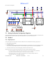
1
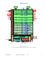
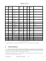
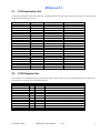
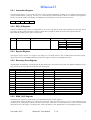
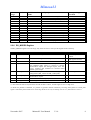
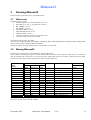
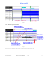
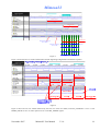
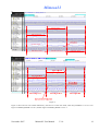
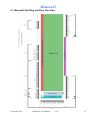
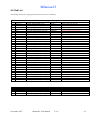
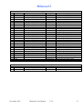
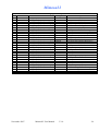
Mimosa22 User Manual (Preliminary version) A. Himmi, G. Bertolone, A. Brogna, W. Dulinski, C. Colledani, A. Dorokhov, Ch. Hu, F. Morel, I.Valin Institut de Recherches Subatomiques IN2P3-CNRS / ULP Strasbourg – France Y. Degerli, F. Gilloux CEA Saclay DAPNIA/SEDI CENTRE NATIONAL DE LA RECHERCHE SCIENTIFIQUE INSTITUT NATIONAL DE PHYSIQUE NUCLEAIRE P HYSIQUE DES P ARTICULES ET DE Document history Version Date Description 1.0 Based on Mimosa16 Version November 2007 Mimosa22 chip Version Date 1.0 Description Submitted October 07 AMS 035 Opto Version, 576 x 136 pixels CENTRE NATIONAL DE LA RECHERCHE SCIENTIFIQUE INSTITUT NATIONAL DE PHYSIQUE NUCLEAIRE P HYSIQUE DES P ARTICULES ET DE Comments Preliminary version Mimosa22 1 2 Introduction ........................................................................................................................ 3 Control Interface ................................................................................................................ 5 2.1 JTAG Instruction Set.................................................................................................. 6 2.2 JTAG Register Set...................................................................................................... 6 2.2.1 Instruction Register ............................................................................................ 7 2.2.2 DEV_ID Register ............................................................................................... 7 2.2.3 Bypass Register .................................................................................................. 7 2.2.4 Boundary Scan Register ..................................................................................... 7 2.2.5 BIAS_DAC Register .......................................................................................... 7 2.2.6 RO_MODE0 Register ........................................................................................ 8 2.2.7 RO_MODE1 Register ........................................................................................ 9 2.2.8 CONTROL_REG Register................................................................................. 9 2.2.9 SEQUENCER_REG Register .......................................................................... 10 2.2.10 DIS_DISCRI Register ...................................................................................... 12 2.2.11 LINEPAT_REG Register................................................................................. 12 3 Running Mimosa22 .......................................................................................................... 13 3.1 After reset................................................................................................................. 13 3.2 Biasing Mimosa22.................................................................................................... 13 3.3 Setting the Readout Configuration Registers ........................................................... 14 3.4 Readout..................................................................................................................... 14 3.4.1 Signal protocol ................................................................................................. 14 3.4.2 Successive frames and resynchronisation ........................................................ 15 3.5 Analogue and digital Data Format ........................................................................... 15 3.5.1 Normal mode data format ................................................................................ 15 3.5.2 Test mode data format...................................................................................... 16 3.6 Mimosa22 Chronograms .......................................................................................... 16 3.6.1 Normal Readout ............................................................................................... 16 3.6.2 Readout synchronisation .................................................................................. 17 3.6.3 Main Signal Specifications............................................................................... 20 4 Pad Ring ........................................................................................................................... 20 4.1 Mimosa22 Pad Ring and Floor Plan View............................................................... 21 4.2 Pad List..................................................................................................................... 22 November 2007 Mimosa22 User Manual V.1.0 2 Mimosa22 1 Introduction Mimosa22 is intermediate prototype before the final sensor chip of EUDET JRA1 beam telescope for the ILC vertex detector studies. Its architecture is based on the Mimosa16 which is a fast binary readout Monolithic Active Pixel Sensor (MAPS). Mimosa22 has been designed in AMSC35B4O1 CMOS-Opto 0.35 µm.This CMOS-Opto process has 4 metal layers and 2 poly layers, and uses 14 µm epitaxial wafers. The Process Design Kit V3.70 has been provided by CMP. The design tools are CADENCE DFII 5.1 with DIVA, ASSURA, CALIBRE rules. The chip has been submitted in a Multi Chip Run via CMP the 26 October 2007 in the run # A35C5-4. The sensor matrix is composed by 576 x 136 pixels of 18.4 µm pitch which are based on self biased diode and the reset diode architectures. The chip consists of seventeen sub- array of pixels, 128 column-level discriminators for signal sparsification, a fully programmable digital sequencer and output multiplexers for binary outputs. The operation sequence of Mimosa22 is: 1. 2. Power On Reset or Reset on RstB pad (active at low level) Setup of the chip with programmable registers accessed via an embedded slow control Jtag interface: • • 3. Load the DACs which bias the analogue blocks If necessary, load the ReadOut Register with a specific configuration. The default setup on power on reset allows a normal readout once the biases have been set. Readout of the chip • The chip is driven by a 100 MHz clock. The readout starts when the input “START” token has its rising signal sampled by the internal 100 MHz clock. • Few digital markers are available for the control of the readout process • Pixels are sequentially read out in a specific order explained later in the document • Successive pixel frames are read until the readout clock is stopped. A frame resynchronisation can be performed at any time by setting up the “START” token again. November 2007 Mimosa22 User Manual V.1.0 3 November 2007 Mimosa22 User Manual V.1.0 Aout <0> Aout <7> Dout <0> Dout <7> SPEAK CkCMOS CkRdLp CkRdLn START MK_CLK_D MK_CLK_A CLKA CLKD Tst2Pad Tst1Pad RstB TCK TDI TMS TDO Dout <8> Dout <15> AnaDriver <7:0> MUX 8 to1 MUX 8 to1 MUX 8 to1 MUX 8 to1 Rows Address Registre<575:0> Multiplexer Row Pix Mimosa22 Mimosa22 functional view Does not correspond to the floorplan neither for the core, neither for the pad ring 4 Mimosa22 Test matrix S1 S2 S3 S4 S5 Row addresses range 15-0 31-16 79-32 95-80 159-96 S6 223-160 S7 287-224 S8 303-288 S9 319-304 S10 351-320 S11 383-352 S12 415-384 S13 S14 447-416 479-448 S15 S16 S17 511-480 543-512 575-544 Circuit type High gain CS + Time-variant feedback High gain CS +Time-variant feedback High gain CS + Time-variant feedback High gain CS + Time-variant feedback High gain CS + Time-variant feedback High gain CS + Self-biased High gain CS + Self-biased High gain CS + Self-biased High gain CS + Self-biased High gain CS + Reset High gain CS + Time-variant feedback High gain CS + Reset CS + Reset CS + Timevariant feedback CS + Reset CS + Reset CS + Reset Diode area (µm2) V_Clp (V) Vdd_ diode (V) Row Number 4.5x4.5 2.1-2.4 - 16 3.8x3.8 2.1-2.4 - 16 3.8x3.8 2.1-2.4 - 48 Name CSTVF_tst1 CSTVF_tst2 CSTVF_RadTol (1) CSTVF_RadTol_poverlap 3.8x3.8 2.1-2.4 - 16 (1) CSTVF_STD 3.8x3.8 2.1-2.4 - 64 4.3x3.4 2.1-2.4 - 64 4.3x3.4 2.1-2.4 - 64 4.4x4.4 2.1-2.4 - 16 3.4x3.4 2.1-2.4 - 16 3.85x3.95 2.1 0.9 32 3.375x4.5 2.1 - 32 3.375x4.5 2.1 0.9 32 3.85x3.95 2.1 0.9 32 3.375x4.5 2.1 - 32 3.375x4.5 3.375x4.5 3.45x3.625 2.1 2.1 2.1 0.9 1.05 1.05 32 32 32 CSFB_RadTol (1) CSFB_STD CSFB_tst1 CSFB_tst2 Pix_CSG10_D2RadTol Pix_CSG10ActRst_D2 Pix_CSG10_D2 Pix_CSG7_D2RadTol Pix_CSG7ActRst_D2 Pix_CSG7_D2 Pix_CSG5_D2 Pix_CSG5_D1 Summary of pixel matrix (1) For the RadTol pixel, the Voltage name RadTolPixGate is set to 0 V by default value or can be adjustable. 2 Control Interface The control interface of Mimosa22 complies with Boundary Scan, JTAG, IEEE 1149.1 Rev1999 standard. It allows the access to the internal registers of the chip like the bias Register and the different registers control. On Power-On -Reset, an internal reset for the control interface is generated. The finite state machine of the Test Access Port (TAP) of the controller enters in the Test-Logic-Reset state and the ID register is selected. Mimosa22 has been designed in order to be fully adjustable via the control interface. Nevertheless several voltages level can be set both via the control interface a via a pad. November 2007 Mimosa22 User Manual V.1.0 5 Mimosa22 2.1 JTAG Instruction Set The Instruction Register of the JTAG controller is loaded with the code of the desired operation to perform or with the code of the desired data register to access. Instruction 5 Bit Code16 Selected Register Notes EXTEST 01 BSR JTAG mandatory instruction HIGHZ 02 BYPASS JTAG mandatory instruction INTEST 03 BSR JTAG mandatory instruction CLAMP 04 BYPASS JTAG mandatory instruction SAMPLE_PRELOAD 05 BSR JTAG mandatory instruction ID_CODE 0E DEV_ID register User instruction BIAS_GEN 0F BIAS_DAC User instruction PATTERN_REG 10 LINEPAT_REG User instruction DIS_LATCH 11 DIS_DISCRI User instruction SEQ_REG 12 SEQUENCER_REG User instruction CTRL_REG 13 CONTROLER_REG User instruction NU1 14 (1) Reserved, Not Used NU2 15 (1) Reserved, Not Used NU3 16 (1) Reserved, Not Used NU4 17 (1) Reserved, Not Used NU5 18 (1) Reserved, Not Used NU6 19 (1) Reserved, Not Used NU7 1A (1) Reserved, Not Used NU8 1B (1) Reserved, Not Used NU9 1C (1) Reserved, Not Used RO_MODE1 1D ReadOut Mode 1 User instruction RO_MODE0 1E ReadOut Mode 0 User instruction BYPASS 1F BYPASS JTAG mandatory instruction (1) Instruction codes implemented but not the corresponding registers. To be fixed in the next version. 2.2 JTAG Register Set JTAG registers are implemented with a Capture/Shift register and an Update register. JTAG standard imposes that the last significant bit of a register is downloaded/shifted first. Register Name Size Access Notes INSTRUCTION REG DEV_ID BYPASS BSR BIAS_DAC RO_MODE0 RO_MODE1 CONTROL_REG SEQUENCER_REG DIS_DISCRI LINEPAT_REG NU1,NU2,…,NU9 5 32 1 10 120 8 8 40 128 128 128 0 R/W R Only R Only R/W R/W R/W R/W R/W R/W R/W R/W - Instruction Register November 2007 Previous value shifted out during write Previous value shifted out during write Previous value shifted out during write Previous value shifted out during write Previous value shifted out during write Previous value shifted out during write Previous value shifted out during write Not implemented. For future use Mimosa22 User Manual V.1.0 6 Mimosa22 2.2.1 Instruction Register The Instruction register is a part of the Test Access Port Controller defined by the IEEE 1149.1 standard. The Instruction register of Mimosa22 is 5 bits long. On reset, it is set with the ID_CODE instruction. When it is read the 2 last significant bits are set with the markers specified by the standard, the remaining bits contain the current instruction. X X X 1 0 2.2.2 DEV_ID Register The Device Identification register is implemented. It is 32 bits long and has fixed value hardwired into the chip. When selected by the ID_CODE instruction or after the fixed value is shifted via TDO, the JTAG serial output of the chip. Mimosa22 ID_CODE register value is 0x4D323201. Bit # Bit Name Purpose Default value Code16 31-0 ID_CODE Device Identification register 4D323201 ASCII ‘M’ ‘2’ ‘2’ <SOH> HEX 4D 32 32 01 2.2.3 Bypass Register The Bypass register consists of a single bit scan register. It is selected when its code is loaded in the Instruction register, during some actions on the BSR and when the Instruction register contains an undefined instruction. 2.2.4 Boundary Scan Register The Boundary Scan Register, according with the Jtag instructions, tests and set the IO pads. The Mimosa22 BSR is 10 bits long and allows the test of the following input and outputs pads. Bit # Corresponding Pad Type Signal Notes 9 8 7 6 SPEAK CkCMOS START LVDS CkRdLn/CkRdLp Input Input Input Input SPEAK CkCMOS START ClkLvds 5 4 3 2 1 0 MK_CLK_D MK_CLK_A CLKD CLKA Tst2Pad Tst1Pad Ouput Ouput Ouput Ouput Ouput Ouput MK_CLK_D MK_CLK_A CLKD CLKA Tst2Pad Tst1Pad Active Readout Marker & Clock CMOS Clock Readout : Input synchronisation Resulting CMOS signal after LVDS Receiver Readout : Digital Marker & Clock Readout : Analogue Marker & Clock Readout Digital Clock Readout Analogue Clock Readout Test Pad 2 Readout Test Pad 1 2.2.5 BIAS_DAC Register The BIAS_DAC register is 120 bit wide; it sets simultaneously the 15 DAC registers. As show bellow these 8-bit DACs set voltage and current bias. After reset the register is set to 0, a value which fixes the minimum power consumption of the circuit. The current values of the DACs are read while the new values are downloaded during the access to the register. An image of the value of each DAC can be measured on its corresponding test pad. November 2007 Mimosa22 User Manual V.1.0 7 Mimosa22 Bit range DAC # DAC Internal Name DAC purpose Corresponding Test Pad 119-105 111-104 103-96 95-88 87-73 79-72 71-64 63-56 55-48 47-40 39-32 31-24 23-16 15-8 7-0 DAC14 DAC13 DAC12 DAC11 DAC10 DAC9 DAC8 DAC7 DAC6 DAC5 DAC4 DAC3 DAC2 DAC1 DAC0 IKIMO IPIX IVTST2 IVTST1 IDIS2 IDIS1 IVDREF2 IVDREF1 IAnaBUF ILVDS ID2PWRS ID1PWRS IBufBias IPwrSWBias ICLPDISC External circuit monitoring Pixel source follower bias Test Level, emulates a pixel output IDEM Discriminator bias 2 Discriminator bias 1 Discriminator Reference 2 Discriminator Reference 1 Analogue Buffer bias LVDS PAD bias Discriminator bias 2 (mode low consp.) Discriminator bias 1 (mode low consp.) Ref&Tst Buffer bias Discriminator Power Pulse bias Discriminator Clamping bias VKIMO IPIX VTEST2 VTEST1 IDIS2 IDIS1 VDREF2 VDREF1 IAnaBUF ILVDS BUFBIAS PWRSWBIAS DISCLP 2.2.6 RO_MODE0 Register The RO_MODE0 registers are 8 bits large; they allow the user to select specific digital mode of the chip. Bit # Bit Name Purpose Basic configuration value 7 En_TstBuf Enable the internal injection of VTEST 0 6 En_HalfMatrx Set the row shift register to 320 in place of 576 bits. 0 5 4 DisLVDS En_LineMarker 0 0 3 MODE_SPEAK 0 Marker signal active 2 Pattern_Only 0 Normal mode 1 0 En_ExtStart JTAG_Start Disable LVDS and active clock CMOS. Add two rows at the end of matrix for a chip Readout: The LINEPAT_REG register is selected to emulate discriminators outputs. For analogue outputs, the 2 Test Levels, VTEST1 and VTEST2 are selected which emulate a pixel output. Select Marker signal or Readout Clock for digital and analogue data (MK_CLKA and MK_CLKD pads) Test Mode: Select LINEPAT_REG to emulate discriminators outputs Enable external START input synchronisation (1) Enable Jtag START input synchronisation (2) External injection of VTEST Normal mode, 576 row shift register selected LVDS selected Normal mode 0 0 Normal mode (1) The minimum wide of asynchronous external START is 500 ns, and this signal is active at high level. (2) When En_ExtStart is disabled, it’s possible to generate internal START by accessing JTAG_Start bit. JTAG_Start signal is realized by three JTAG access: First step, this bit is set to 0, second step it is set to 1, and at last it is set to 0. November 2007 Mimosa22 User Manual V.1.0 8 Mimosa22 2.2.7 RO_MODE1 Register The RO_MODE1 registers are 8 bits large; they allow selecting specific analogue mode of the chip. Bit # Bit Name Purpose 7 6 5 4 3 2 1 0 NU4 NU3 NU2 DisBufRef NU1 En_AOP_Disc En_Pulse_Discri En_TstDis Reserved, Not Used Reserved, Not Used Reserved, Not Used Disable the internal reference Reserved, Not Used Enable the Power pulse Amplifier Enable the discri power pulse mode Enable the discri. test mode Basic configuration value 0 Select Internal Buffer 0 0 0 Normal mode Normal mode Normal mode 2.2.8 CONTROL_REG Register The CONTROL_REG registers are 40 bits large; they allow setting parameters of the readout controller. Bit # Bit Name Purpose Basic configuration value Code16 39-36 35-33 32-30 29-20 NU SelPad1 SelPad2 RowMkLast 0 0 0 023F 19-10 RowMkd 9-0 RowMka Reserved, Not Used Selection bit of Test1Pad Selection bit of Test2Pad Row number of the frame. It depends of readout mode. When the En_HalfMatrx mode is active, the value is 0x013F otherwise 0x023F. When the En_LineMarker mode is active, add two rows at the end of matrix. Selection parameter of row for digital marker (MK_Test_D) Selection parameter of row for analogue marker (MK_Test_A) November 2007 Mimosa22 User Manual 0 0 V.1.0 MK_Test_A signal MK_Test_D signal Normal mode, the number of row matrix is 576. Digital marker place is first row of matrix during the readout analogue marker place is first row of matrix during the readout 9 Mimosa22 The purpose of this array is to describe the internal signals which can be checked using 2 test pads (Tst1Pad and tst2Pad). The internal signals can be selected with SelPad1 and SelPad2 bits. SelPad1 Tst1Pad Purpose SelPad2 Tst2Pad Purpose 0 MK_Test_A 0 MK_Test_D Digital marker corresponding to last serialized digital data. It depends of RowMkd selection parameter. 1 Mk_Rd 1 PwrOns Same signal as PwOn, but shifted of 16 main clock 2 Mk_Calib 2 PwOn Activate power supply for pixel 3 CkDiv32 3 SlcRowInt 4 MK_A 4 Clp Connect pixel output to common column Set reference voltage for clamping 5 Clp 5 RstDiode 6 Latch 6 Rd 7 CkDiv16 Analogue marker is shifted of 80 ns to MK_A signal. This signal rises up at the beginning read phase and falls down at the end of Calib phase. It depends of RowMka selection parameter. Analogue marker corresponding to Rd phase of readout pixel. It depends of RowMka selection parameter Analogue marker corresponding to Calib phase of readout pixel. It depends of RowMka selection parameter CkDiv16 signal is devised by 2 Analogue marker corresponding to readout pixel sequence. It depends of RowMka selection parameter. Set reference voltage for clamping Latch state of the discriminator Main Clock is devised by 16 7 Calib Set reference voltage for diode Sample before clamping Sample after clamping 2.2.9 SEQUENCER_REG Register The SEQUENCER_REG registers are 128 bits large; this register contains all parameters to generate readout pixel and discriminator sequence. Bit # Bit Name Purpose 127-112 DataRdPix 111-96 DataRst1 95-80 DataClp 79-64 63-48 47-32 DataCalib DataRdDsc DataLatch 31-0 DataPwrOn Connect pixel output common column Set reference voltage diode Set reference voltage clamping Sample after clamping Sample before clamping Latch state of discriminator Activate power supply pixel November 2007 Basic configuration value Code16 Signal Name to 7FFF Slct_Row_Int for 0040 Rst for 01C0 Clamp the 3C00 001C 6000 Calib Read Latch for 7FFFFFFF Mimosa22 User Manual (1) Pwr_On V.1.0 10 Mimosa22 (1) Example: Generation of Latch Signal Msb • Lsb 15 14 13 12 11 10 9 8 7 6 5 4 3 2 1 0 0 1 1 0 0 0 0 0 0 0 0 0 0 0 0 0 Related timing with fClkL=100 MHz (Read, Calib, Latch signals are used by the column readout circuitry). For Sub arrays S6-S9, S11 and S14, the Rst signal is not used for pixel. • This is readout sequence of the pixel and discriminator for 2 successive rows of matrix. In the wave form, the indexation of internal signal vectors is reversed compared with the Mimosa22 functional view (for example, the signal Pwr_On[575] corresponds to the row at the top of matrix). For Sub arrays S10-S17, the Pwr_On signal is not used for pixel. November 2007 Mimosa22 User Manual V.1.0 11 Mimosa22 2.2.10 DIS_DISCRI Register The DIS_DISCRI register is 128 bits large. The purpose of this register is to disable the discriminator on a specific column if it is noisy, by gating Latch signal and setting the output discriminator at 0. The default value of the DIS_DISCRI register is 0; it means that all discriminators are activated. Setting a bit to 1 disables the corresponding discriminator. In Mimosa22, the DisableLatch<127> is on the left hand side while DisableLatch<0> is on the right hand side. 127 (Msb) 0 (Lsb) DisableLatch<127> DisableLatch<0> 2.2.11 LINEPAT_REG Register The LINEPAT_REG register is 128 bits large. The purpose of this register is to emulate discriminators outputs rows in En_LineMarker and Pattern_Only modes. When Pattern_Only is active, during the readout of matrix, the value of LINEPAT_REG is read to emulate discriminators outputs of each matrix row. This mode corresponds to debug mode, it allows verify the digital processing. In the En_LineMarker mode, it adds two rows at the end of matrix for a readout chip and the LINEPAT_REG register is read to emulate the discriminators outputs of these two supplementary rows. This mode allows generating pattern marker in matrix data frame to detect chip readout desynchronization. Bit # Bit Name Purpose Basic configuration value Code16 127-0 LinePatReg Emulate discriminators rows AAFFFFFF_AAAAAAAA_55555555_22FFFF11 (1) (1) Example of pattern used in simulation. November 2007 Mimosa22 User Manual V.1.0 12 Mimosa22 3 Running Mimosa22 The following steps describe how to operate Mimosa22 3.1 After reset On RstB active low signal: • All BIAS registers are set to the default value, i.e. 0 • DIS_DISC is set to 0, i.e. all columns are selected • RO_MODE0 is set to 0 • RO_MODE1 is set to 0 • CONTROL_REG is set to 0 • SEQUENCER_REG is set to 0 • LINEPAT_REG is set to 0 • JTAG state machine is in the Test-Logic-Reset state • JTAG ID_CODE instruction is selected Then the bias register has to be loaded. The same for the RO_MODE0, RO_MODE1, CONTROL_REG, SEQUENCER_REG, LINEPAT_REG and DIS_DISC registers if the running conditions differ from defaults. Finally the readout can be performed either in normal mode or in test mode. 3.2 Biasing Mimosa22 The BIAS_DAC register has to be loaded before operating Mimosa22. The 15 DACs constituting this register are built with the same 8 bits DAC current generator which has a 1 µA resolution. Specific interfaces like current mirror for current sourcing or sinking and resistors for voltages, customise each bias output. The following table shows the downloaded codes which set the nominal bias. Internal DAC Name IKIMO IPIX IVTST2 IVTST1 IDIS2 IDIS1 IVDREF2 IVDREF1 IAnaBUF ILVDS ID2PWRS ID1PWRS IBufBias IPwrSWBias ICLPDISC Code16 Code10 64-100 32-50 71-113 8C-140 20-32 20-32 71-113 80-128 32-50 20-32 A-10 A-10 A-10 A-10 64-100 Simulation DacInternal current-µA 100 50 113 140 32 32 113 128 50 32 10 10 10 10 100 Resolution Output value 1V 50 µA 1.182 V 1.183 V 5 µA 10 µA 1.182 V 1.182 V 500 µA 7 µA 100 nA 100 nA 10 µA 10 µA 2.1 V 10 mV 1 µA 10 mV 250 µV 156 nA 312 nA 10 mV 250 µV 10 µA 218 nA 10 nA 10 nA 1 µA 1 µA 10 mV Range Experimental Code16 Code10 From 0 up to 2.55 V From 0 up to 255 µA From 1 up to 1.5 V From -30 up to 34 mV From 0 up to 255 µA From 0 up to 255 µA From 1 up to 1.5 V From -30 up to 34 mV (1) From 0 up to 255 µA From 0 up to 255 µA From 0 up to 255 µA From 0 up to 255 µA From 0 up to 255 µA From 0 up to 255 µA From 1.2 up to 3.2 V (1) Referenced with respect to IVDREF2. The threshold voltage of the discriminators ∆Vth is defined as Vref1-Vref2 (Vref1=Vref2+∆Vth). November 2007 Mimosa22 User Manual V.1.0 13 Mimosa22 3.3 Pad Pad Pad Pad Pad Pad Pad Pad Pad Pad Bias synthetic block diagram Setting the Readout Configuration Registers If the desired operating mode does not correspond to the default one, set RO_MODE0, RO_MODE1, CONTROL_REG, SEQUENCER_REG, LINEPAT_REG registers following the §2.2.6, §2.2.7, §2.2.8, §2.2.9, §2.2.11. 3.4 Readout 3.4.1 Signal protocol After JTAG registers have been loaded, the readout of Mimosa22 can be initialized with following signal protocol: • • • Start readout clock (CK100M); Set SPEAK signal to 0; Set START signal to 1 during 500 ns (minimum).The internal reset is created after 15 ns on the rising edge of START. After this reset, Clk50M (input clock with a ½ ratio) and CkDiv16 (input clock with 1/16 ratio) are generated; • The readout controller starts at the first falling edge of CkDiv16 after START set to 0. Signal markers allow the readout monitoring and the data outputs (analogue and digital) sampling: CLKA and CLKD are running when readout controller starts. CLKA is signal which is generated by logic OR between Read and Calib signals. And CLKD corresponds to Clk50M; When SPEAK signal is active, markers of synchronisation for analogue and digital outputs are generated on MK_CLK_A and MK_CLK_D pads. November 2007 Mimosa22 User Manual V.1.0 14 Mimosa22 3.4.2 Successive frames and resynchronisation Successive pixel frames are read until the readout clock is stopped. A frame resynchronisation can be performed at any time by setting up the “START” token again. SPEAK signal allows to generate markers signals which are used by DAQ. When SPEAK signal is set to 1 during the current frame, analogue marker appears on MK_SYNC_CLK_A pad and digital marker appears on MK_SYNC_CLK_D pad during next frame. In the MODE_SPEAK=’0’ (see Figure 5.a), the MK_SYNC_CLK_A marker corresponds to last row of the frame and the MK_SYNC_CLK_D marker corresponds to last bit frame. In the MODE_SPEAK=’1’ (see Figure 5.b), MK_SYNC_CLK_A signal corresponds to a sampling clock for analogue outputs data (same as CLKA) which starts at the first row of frame. MK_SYNC_CLK_D signal corresponds to readout clock for digital data (same as CLKD) which starts at the first bit frame. When SPEAK signal is set to 0, MK_SYNC_CLK_A and MK_SYNC_CLK_D are set to 0. 3.5 Analogue and digital Data Format Two Types of signal can be generated on analogue outputs: • Normal pixel signal • Test signal In concern to digital outputs, two types of signal can be generated: • Digitalization pixel signal by discriminator • Test pattern , read to LINEPAT_REG register 3.5.1 Normal mode data format The chip has columns parallel process readout. The first 128 columns are connected to discriminators, multiplexed onto 16 outputs. The last 8 columns of 136 are connected to output analogue buffers. Their analogue outputs can be observed directly on the output pads. The digital part includes three blocks. One is JTAG controller interface which allows configure the internal registers used to readout chip. The second circuit generates the patterns necessary for addressing, resetting and double sampling of the signals in pixels in a column parallel way. The rows are selected sequentially using a multiplexer every 16 clock cycles. The last circuit realizes a temporal multiplexing of the binary outputs at a frequency value half that of the main clock frequency. For Mimosa22, Col.127 is at the left of matrix and Col.0 is at the right. The row at the top of matrix is read out first. 16 multiplexers (8:1) serialize the digital row data onto 16 output pads. The bit which is first selected in the serial 8 bits stream corresponds to the Msb bit (see the table below). Data are serialized on falling edge clock of CLKD. The Vref1 voltage is applied to the negative discriminator input during the read phase and the Vref2 voltage is applied during the Calib phase. The difference voltage Vref1 – Vref2 set the threshold of the discriminator. Voltages can be adjustable via 2 DACs or can be provided via 2 pads. November 2007 Mimosa22 User Manual V.1.0 15 Mimosa22 Output pad Digital output (Msb) (Lsb) Dout<15> Col.127 Col.126 Col.125 Col.124 Col.123 Col.122 Col.121 Col.120 Dout<14> Col.119 Col.118 Col.117 Col.116 Col.115 Col.114 Col.113 Col.112 Dout<13> Col.111 Col.110 Col.109 Col.108 Col.107 Col.106 Col.105 Col.104 Dout<12> Col.103 Col.102 Col.101 Col.100 Col.99 Col.98 Dout<11> Col.95 Col.94 Col.93 Col.92 Col.91 Col.90 Col.89 Col.88 Dout<10> Col.87 Col.86 Col.85 Col.84 Col.83 Col.82 Col.81 Col.80 Dout<9> Col.79 Col.78 Col.77 Col.76 Col.75 Col.74 Col.73 Col.72 Dout<8> Col.71 Col.70 Col.69 Col.68 Col.67 Col.66 Col.65 Col.64 Dout<7> Col.63 Col.62 Col.61 Col.60 Col.59 Col.58 Col.57 Col.56 Dout<6> Col.55 Col.54 Col.53 Col.52 Col.51 Col.50 Col.49 Col.48 Dout<5> Col.47 Col.46 Col.45 Col.44 Col.43 Col.42 Col.41 Col.40 Dout<4> Col.39 Col.38 Col.37 Col.36 Col.35 Col.34 Col.33 Col.32 Dout<3> Col.31 Col.30 Col.29 Col.28 Col.27 Col.26 Col.25 Col.24 Dout<2> Col.23 Col.22 Col.21 Col.20 Col.19 Col.18 Col.17 Col.16 Dout<1> Col.15 Col.14 Col.13 Col.12 Col.11 Col.10 Col.9 Col.8 Dout<0> Col.7 Col.6 Col.5 Col.4 Col.2 Col.1 Col.0 Col.3 Col.97 Col.96 3.5.2 Test mode data format This test readout mode allows obtain the transfer function of discriminator and calibrate the pixel readout chain. During the test mode the pixel matrix is not connected to discriminators and output analogue buffers. Instead of this, two test levels Vtst1, Vtst2 are connected to discriminator inputs to emulate pixel signal. The Vtst1 voltage is applied to the positive discriminator input during the Read phase and the Vtst2 voltage is applied during the Calib phase. Voltages can be adjustable via 2 DACs or can be provided via 2 pads. The difference voltage Vtst1 – Vtst2 corresponds to the pixel output signal. 3.6 Mimosa22 Chronograms The following chronograms describe typical access to the chip; Reset, JTAG download sequence and then the readout. 3.6.1 Normal Readout Figure 1 show the beginning of typical data readout mode. After Reset and JTAG setting, one can see the initialisation phase of the readout of the first pixel row. November 2007 Mimosa22 User Manual V.1.0 16 Mimosa22 Figure 1 3.6.2 Readout synchronisation Figure 2 Figure 2 zoom on the readout start. After a latency of 5 CkDiv16 cycles, readout of matrix starts. November 2007 Mimosa22 User Manual V.1.0 17 Mimosa22 Data Ana. Row 0 Data Ana. Row 1 Data Discri Row 0 Data Discri Row 1 Col. 122 Col. 121 Col. 120 Col. 1 Col. 0 Col. 123 Dout<15> Col. 2 Col. 124 Col. 4 Col. 5 Col. 6 Col. 7 …. Dout<0> …. Col. 3 Col. 125 Col. 126 Sample after clamping of Row 0 (Calib) Col. 127 Sample before clamping of Row 0 (Read) Figure 3 Figure 3 shows the first row of the readout matrix and the beginning of digital data serialization sequence. Figure 4 Figure 4 shows the last row readout followed by the first row of the next frame, when En_LineMarker is set to 1 and MODE_SPEAK is set to 0. These options are set via the RO_MODE0 register. November 2007 Mimosa22 User Manual V.1.0 18 Mimosa22 a) En_LineMarker = 0 MODE_SPEAK = 0 Data Ana. Row 0 Data Ana. Row 575 Last bit frame of serialization Last Row of frame Data Discri. Row 574 Data Discri. Row 575 Data Discri. Row 0 b) Figure 5 Figure 5 shows the last row readout followed by the first row of the next frame, when En_LineMarker is set to 0. For Figure 5.a MODE_SPEAK is set to 0, and for Figure 5.b MODE_SPEAK is set to 1. November 2007 Mimosa22 User Manual V.1.0 19 Mimosa22 3.6.3 Main Signal Specifications Parameter INIT RSTB Pulse Width TCK Frequency JTAG TMS Setup/Hold Time TDI Setup/Hold Time READOUT CKRD Frequency CKRD Duty Cycle START Setup/Hold Time SPEAK Setup/Hold Time Input Dynamic range Rise time Analogue Fall time Driver Bandwidth Output Current Range Typical Value >1 µS 10 MHz ~10 nS ~10 nS Up to 100 MHz 50% 5 nS 5 nS Notes Active Low, Asynchronous Power on Reset Boundary Scan Clock Boundary Scan Control Signal Boundary Scan Serial Data In Readout Clock LVDS signal Chip Initialisation, CMOS signal. Active Readout Marker & Clock 4 Pad Ring The pad ring of Mimosa22 is build with • Pads full custom designed for some of the analogue signals and power supplies • Pads from the AMS library for the digital signals and power supplies The pad ring is split in 8 functional independent parts CMOS JTAG and Test purpose pads LVDS Read Out Drivers Digital outputs Read Out Analogue Outputs Bias Test Analogue and Digital Power supplies Test structure 1 Test structure 2 Each part has its own supply pads. November 2007 Mimosa22 User Manual V.1.0 20 Mimosa22 4.1 Mimosa22 Pad Ring and Floor Plan View November 2007 Mimosa22 User Manual V.1.0 21 Mimosa22 4.2 Pad List The bonding of the power supply pads specified in red colour is mandatory Pad 1 2 3 4 5 6 7 8 9 10 11 12 13 14 15 16 17 18 19 20 21 22 23 24 25 26 27 28 29 30 31 173 174 Name Dout<15> Dout<14> gnd Dout<13> gnd Dout<12> gnd Dout<11> vdd Dout<10> gnd Dout<9> gnd Dout<8> gnd Dout<7> gnd Dout<6> gnd Dout<5> vdd Dout<4> gnd Dout<3> gnd Dout<2> gnd Dout<1> gnd Dout<0> vdd CkCMOS vdd Pad Name 32 vdd_latch 33 gnd November 2007 Pad ring segment 1 – P_D1 Pad General Function PadType Tri-State Output Buffer, 2 mA BT2P Tri-State Output Buffer, 2 mA BT2P Output buffer ground GND3OP Tri-State Output Buffer, 2 mA BT2P Core logic and periphery cells gnd GND3RP Tri-State Output Buffer, 2 mA BT2P Output buffer ground GND3OP Tri-State Output Buffer, 2 mA BT2P Output buffer supply VDD3OP Tri-State Output Buffer, 2 mA BT2P Core logic and periphery cells gnd GND3RP Tri-State Output Buffer, 2 mA BT2P Output buffer ground GND3OP Tri-State Output Buffer, 2 mA BT2P Core logic and periphery cells gnd GND3RP Tri-State Output Buffer, 2 mA BT2P Output buffer ground GND3OP Tri-State Output Buffer, 2 mA BT2P Core logic and periphery cells gnd GND3RP Tri-State Output Buffer, 2 mA BT2P Output buffer supply VDD3OP Tri-State Output Buffer, 2 mA BT2P Output buffer ground GND3OP Tri-State Output Buffer, 2 mA BT2P Core logic and periphery cells gnd GND3RP Tri-State Output Buffer, 2 mA BT2P Output buffer ground GND3OP Tri-State Output Buffer, 2 mA BT2P Core logic and periphery cells gnd GND3RP Tri-State Output Buffer, 2 mA BT2P Core logic and periphery cells supply VDD3RP Clock buffer, 2 mA ICCK2P Core logic and periphery cells supply VDD3RP Function for the chip Digital Output ch. 127-120 Digital Output ch. 119-112 Output buffer ground Digital Output ch. 111-104 Digital ground, periphery & core Digital Output ch. 103-96 Output buffer ground Digital Output ch. 95-88 Output buffer supply Digital Output ch. 87-80 Digital ground, periphery & core Digital Output ch. 79-72 Output buffer ground Digital Output ch. 71-64 Digital ground, periphery & core Digital Output ch. 63-56 Output buffer ground Digital Output ch. 55-48 Digital ground, periphery & core Digital Output ch. 47-40 Output buffer supply Digital Output ch. 39-32 Output buffer ground Digital Output ch. 31-24 Digital ground, periphery & core Digital Output ch. 23-16Output buffer ground Digital Output ch. 15-8 Digital ground, periphery & core Digital Output ch. 7-0 Digital supply, periphery & core CMOS clock Digital supply, periphery & core Pad ring segment 1 – P_D2 Pad General Function PadType Function for the chip Core logic and periphery cells supply AVDD3ALLP Supplies periphery & core only for LATCH Core logic and periphery cells ground AGND3ALLP Ground periphery & core only for LATCH Mimosa22 User Manual V.1.0 22 Mimosa22 Pad 34 35 36 37 38 39 40 41 42 43 44 45 46 47 48 49 50 51 52 53 54 55 56 57 58 59 60 61 62 Name vdda gnd gnd v_clp vdda vdda gnd Vtst2 vdd_diode Vtst1 Aout<0> vdda Aout<1> gnd Aout<2> vdda Aout<3> gnd Aout<4> vdda Aout<5> gnd Aout<6> vdda Aout<7> gnd VCLPDIS Vref1 Vref2 Pad Name 63 vdd 64 gnd November 2007 Pad ring segment 1 – P_A1 Pad General Function PadType Core logic and periphery cells supply AVDD3ALLP Core logic and periphery cells gnd AGND3ALLP Core logic and periphery cells gnd AGND3ALLP DIRECTPAD Core logic and periphery cells supply AVDD3ALLP Core logic and periphery cells supply AVDD3ALLP Core logic and periphery cells gnd AGND3ALLP DIRECTPAD DIRECTPAD DIRECTPAD DIRECTPAD Core logic and periphery cells supply AVDD3ALLP DIRECTPAD Core logic and periphery cells gnd AGND3ALLP DIRECTPAD Core logic and periphery cells supply AVDD3ALLP DIRECTPAD Core logic and periphery cells gnd AGND3ALLP DIRECTPAD Core logic and periphery cells supply AVDD3ALLP DIRECTPAD Core logic and periphery cells gnd AGND3ALLP DIRECTPAD Core logic and periphery cells supply AVDD3ALLP DIRECTPAD Core logic and periphery cells gnd AGND3ALLP DIRECTPAD DIRECTPAD DIRECTPAD Function for the chip Analogue Supplies periphery & core Analogue Ground periphery & core Analogue Ground periphery & core Clamping voltage for pixel array Analogue Supplies periphery & core Analogue Supplies periphery & core Analogue Ground periphery & core External injection of Vtest2 Detection diode supply (Dapnia Design) External injection of Vtest1 Analogue output Analogue Supplies periphery & core Analogue output Analogue Ground periphery & core Analogue output Analogue Supplies periphery & core Analogue output Analogue Ground periphery & core Analogue output Analogue Supplies periphery & core Analogue output Analogue Ground periphery & core Analogue output Analogue Supplies periphery & core Analogue output Analogue Ground periphery & core External injection of Discri clamping External injection of Discri Ref1 External injection of Discri Ref2 Pad ring segment 1 – P_D3 Pad General Function PadType Function for the chip Core logic and periphery cells ground AVDD3ALLP Ground periphery & core only for DAC Core logic and periphery cells supply AGND3ALLP Supplies periphery & core only for DAC Mimosa22 User Manual V.1.0 23 Mimosa22 Pad 65 66 67 68 69 70 71 72 73 74 75 76 77 78 79 80 81 82 83 84 85 86 87 88 89 90 91 92 Name ITEST gnd DISCLP vdda PWRSWBIAS gnd BUFBIAS vdda ILVDS gnd IAnaBUF vdda VDR2 gnd VDR1 vdda IDIS2 gnd IDIS1 vdda VTEST2 VTEST1 gnd IPIX vdda VKIMO RADTOLPIXGATE gnd November 2007 Pad ring segment 1 – P_A2 Pad General Function PadType APRIOP Analog I/O pad, 0 Ω serial Core logic and periphery cells gnd AGND3ALLP APRIOP Analog I/O pad, 0 Ω serial Core logic and periphery cells supply AVDD3ALLP APRIOP Analog I/O pad, 0 Ω serial Core logic and periphery cells gnd AGND3ALLP APRIOP Analog I/O pad, 0 Ω serial Core logic and periphery cells supply AVDD3ALLP APRIOP Analog I/O pad, 0 Ω serial Core logic and periphery cells gnd AGND3ALLP APRIOP Analog I/O pad, 0 Ω serial Core logic and periphery cells supply AVDD3ALLP APRIOP Analog I/O pad, 0 Ω serial Core logic and periphery cells gnd AGND3ALLP APRIOP Analog I/O pad, 0 Ω serial Core logic and periphery cells supply AVDD3ALLP APRIOP Analog I/O pad, 0 Ω serial Core logic and periphery cells gnd AGND3ALLP APRIOP Analog I/O pad, 0 Ω serial Core logic and periphery cells supply AVDD3ALLP APRIOP Analog I/O pad, 0 Ω serial APRIOP Analog I/O pad, 0 Ω serial Core logic and periphery cells gnd AGND3ALLP APRIOP Analog I/O pad, 0 Ω serial Core logic and periphery cells supply AVDD3ALLP APRIOP Analog I/O pad, 0 Ω serial APRIOP Analog I/O pad, 0 Ω serial Core logic and periphery cells gnd AGND3ALLP Mimosa22 User Manual V.1.0 Function for the chip Reference current (1µA) Analogue Ground periphery & core DAC Output for Discri Clamping Analogue Supplies periphery & core Discri Power Pulse Voltage Bias Analogue Ground periphery & core DAC output: Ref&Tst Buffer voltage bias Analogue Supplies periphery & core DAC output: LVDS PAD voltage bias Analogue Ground periphery & core Analogue Output Buffer bias Analogue Supplies periphery & core DAC output: Discriminator Reference 2 Analogue Ground periphery & core DAC output: Discriminator Reference 1 Analogue Supplies periphery & core DAC output: Discriminator Bias 2 Analogue Ground periphery & core DAC output: Discriminator Bias 1 Analogue Supplies periphery & core DAC output: VTEST2 DAC output: VTEST1 Analogue Ground periphery & core DAC output: Pixel Array Bias Analogue Supplies periphery & core A reference voltage from DAC output POLY Gate voltage for Andrei RadTol Pix Analogue Ground periphery & core 24 Mimosa22 Pad 125 126 127 128 129 130 131 132 133 134 135 136 137 138 139 140 141 142 143 144 145 146 147 148 149 150 151 152 153 154 155 156 157 158 159 160 161 Name vdd gnd vdd gnd START gnd vdd RstB gnd TDI vdd TDO gnd TCK vdd TMS gnd vdd gnd gnd vdd vdd SPEAK gnd MK_CLK_A Vdd MK_CLK_D gnd CLKD vdd CLKA gnd Tst2Pad vdd Tst1Pad gnd vdd Pad ring segment 1 – P_D4 Pad General Function PadType Core logic and periphery cells supply VDD3RP Core logic and periphery cells gnd GND3RP Output buffer supply VDD3OP Output buffer ground GND3OP CMOS Input Buffer ICP Core logic and periphery cells gnd GND3RP Core logic and periphery cells supply VDD3RP Schmitt-Trigger Input Buffer, Pull Up ISUP Output buffer ground GND3OP CMOS Input Buffer, Pull Up ICUP Output buffer supply VDD3OP Tri-State Output Buffer, 4 mA BT4P Core logic and periphery cells gnd GND3RP CMOS Clock Input Buffer, 2 mA ICCK2P Core logic and periphery cells supply VDD3RP CMOS Input Buffer, Pull Up ICUP Output buffer ground GND3OP Output buffer supply VDD3OP Core logic and periphery cells gnd GND3RP Output buffer ground GND3OP Core logic and periphery cells supply VDD3RP Output buffer supply VDD3OP CMOS Input Buffer ICP Core logic and periphery cells gnd GND3RP Tri-State Output Buffer, 2 mA BT2P Core logic and periphery cells supply VDD3RP Tri-State Output Buffer, 2 mA BT2P Output buffer ground GND3OP Tri-State Output Buffer, 2 mA BT2P Output buffer supply VDD3OP Tri-State Output Buffer, 2 mA BT2P Core logic and periphery cells gnd GND3RP Tri-State Output Buffer, 2 mA BT2P Core logic and periphery cells supply VDD3RP Tri-State Output Buffer, 2 mA BT2P Output buffer ground GND3OP Output buffer supply VDD3OP Pad 162 163 164 165 166 Name TempOut gnd vdda vdda gnd Pad ring segment 1 – P_A3 Pad General Function PadType Direct Pad, no protections DIRECTPAD Core logic and periphery cells ground AGND3ALLP Core logic and periphery cells supply AVDD3ALLP Core logic and periphery cells supply AVDD3ALLP Core logic and periphery cells ground AGND3ALLP Function for the chip Temperature probe output Ground periphery & core Supplies periphery & core Supplies periphery & core Ground periphery & core Pad ring segment 1 – P_D5 Pad General Function PadType Core logic and periphery cells supply VDD3ALLP Core logic and periphery cells gnd GND3ALLP Function for the chip Supplies periphery & core for DAC Ground periphery & core for DAC Pad Name 167 vdd 168 gnd November 2007 Mimosa22 User Manual V.1.0 Function for the chip Digital supply, periphery & core Digital ground, periphery & core Output buffer supply Output buffer ground Readout: Input synchronisation Digital ground, periphery & core Digital supply, periphery & core Asynchronous Active Low Reset Output buffer ground JTAG Control Signal Output buffer supply JTAG Serial Data Out Digital ground, periphery & core JTAG Clock Digital supply, periphery & core JTAG Control Signal Output buffer ground Output buffer supply Digital ground, periphery & core Output buffer ground Digital supply, periphery & core Output buffer supply Active Readout Marker & Clock Digital ground, periphery & core Readout: Analogue Marker & Clock Digital supply, periphery & core Readout: Digital Marker & Clock Output buffer ground Readout Digital clock Output buffer supply Readout Analogue clock Digital ground, periphery & core Readout Test Pad Digital supply, periphery & core Readout Test Pad Output buffer ground Output buffer supply 25 Mimosa22 Pad 169 170 171 172 Name gnd CkRdLp CkRdLn vdd Pad ring segment 1 – P_D6 Pad General Function PadType Core logic and periphery cells ground GND3ALLP LVDS In + Full Custom LVDS In Full Custom Core logic and periphery cells supply VDD3ALLP Function for the chip Ground periphery & core Readout Clock Signal Readout Clock Signal Supplies periphery & core Pad ring segment P_T1 (Pad 94 to 112) and Pad ring segment P_T2 (Pad 113 to 124) are used only for internal test. November 2007 Mimosa22 User Manual V.1.0 26