1
AN4194
Application note
Flash Programming for
SPC560xx, SPC56APxx and SPC563M64xx devices
Introduction
This document describes the operations needed to perform a Flash Programming on
SPC560Bxx, SPC560Cxx, SPC560Dxx, SPC560Pxx, SPC56APxx and SPC563M64xx
Flash.
Supported devices list:
●
SPC560D30xx
●
SPC560D40xx
●
SPC560B40xx
●
SPC560B50xx
●
SPC560C40xx
●
SPC560C50xx
●
SPC560B54xx
●
SPC560B60xx
●
SPC560B64xx
●
SPC560P34xx
●
SPC560P40xx
●
SPC560P44xx
●
SPC560P50xx
●
SPC560P54xx
●
SPC560P60xx
●
SPC56AP54xx
●
SPC56AP60xx
●
SPC563M64xx
September 2013
Doc ID 023880 Rev 2
1/19
www.st.com
Contents
AN4194
Contents
1
Flash memory architecture . . . . . . . . . . . . . . . . . . . . . . . . . . . . . . . . . . . 4
1.1
Code Flash . . . . . . . . . . . . . . . . . . . . . . . . . . . . . . . . . . . . . . . . . . . . . . . . . 5
1.1.1
1.2
Data Flash . . . . . . . . . . . . . . . . . . . . . . . . . . . . . . . . . . . . . . . . . . . . . . . . . 5
1.2.1
2
Main features . . . . . . . . . . . . . . . . . . . . . . . . . . . . . . . . . . . . . . . . . . . . . . 5
Main features . . . . . . . . . . . . . . . . . . . . . . . . . . . . . . . . . . . . . . . . . . . . . . 5
Programming . . . . . . . . . . . . . . . . . . . . . . . . . . . . . . . . . . . . . . . . . . . . . . . 6
2.1
Double word program . . . . . . . . . . . . . . . . . . . . . . . . . . . . . . . . . . . . . . . . . 6
2.2
Sector erase . . . . . . . . . . . . . . . . . . . . . . . . . . . . . . . . . . . . . . . . . . . . . . . . 7
3
Operation modes . . . . . . . . . . . . . . . . . . . . . . . . . . . . . . . . . . . . . . . . . . . . 9
4
Using the Flash library . . . . . . . . . . . . . . . . . . . . . . . . . . . . . . . . . . . . . . 10
4.1
Performing the programming . . . . . . . . . . . . . . . . . . . . . . . . . . . . . . . . . . 10
4.1.1
5
Sample code . . . . . . . . . . . . . . . . . . . . . . . . . . . . . . . . . . . . . . . . . . . . . 11
Library reference . . . . . . . . . . . . . . . . . . . . . . . . . . . . . . . . . . . . . . . . . . . 14
5.1
FlashInit() . . . . . . . . . . . . . . . . . . . . . . . . . . . . . . . . . . . . . . . . . . . . . . . . . 14
5.2
FlashProgram() . . . . . . . . . . . . . . . . . . . . . . . . . . . . . . . . . . . . . . . . . . . . 15
Appendix A Document references . . . . . . . . . . . . . . . . . . . . . . . . . . . . . . . . . . . . 17
Revision history . . . . . . . . . . . . . . . . . . . . . . . . . . . . . . . . . . . . . . . . . . . . . . . . . . . . 18
2/19
Doc ID 023880 Rev 2
AN4194
List of tables
List of tables
Table 1.
Table 2.
Table 3.
Table 4.
Table 5.
Table 6.
Table 7.
Arguments for FlashInit() . . . . . . . . . . . . . . . . . . . . . . . . . . . . . . . . . . . . . . . . . . . . . . . . . . 14
Return values for FlashInit() . . . . . . . . . . . . . . . . . . . . . . . . . . . . . . . . . . . . . . . . . . . . . . . . 14
Troubleshooting for FlashInit . . . . . . . . . . . . . . . . . . . . . . . . . . . . . . . . . . . . . . . . . . . . . . . 14
Arguments for FlashProgram() . . . . . . . . . . . . . . . . . . . . . . . . . . . . . . . . . . . . . . . . . . . . . . 15
Return values for FlashProgram() . . . . . . . . . . . . . . . . . . . . . . . . . . . . . . . . . . . . . . . . . . . 15
Troubleshooting for FlashProgram() . . . . . . . . . . . . . . . . . . . . . . . . . . . . . . . . . . . . . . . . . . 16
Document revision history . . . . . . . . . . . . . . . . . . . . . . . . . . . . . . . . . . . . . . . . . . . . . . . . . 18
Doc ID 023880 Rev 2
3/19
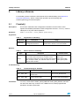
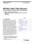
Flash memory architecture
1
AN4194
Flash memory architecture
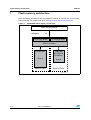
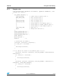
In the SPC560xx, SPC56APxx and SPC563M64xx families we can find one or more Code
Flash block and one of Data Flash block (see Appendix A: Document references).
Figure 1.
SPC560B50 Flash memory architecture
")#$SPTTCBS4XJUDI
")#QPSUT
Y1BHF#VGGFS
Y1BHF#VGGFS
1'MBTI$POUSPMMFS
,#'MBTI
%BUB'MBTI
GPS&&130.
FNVMBUJPO
"SSBZ
"SSBZ
#BOL$'MBTI
#BOL$'MBTI
("1($'5
4/19
Doc ID 023880 Rev 2
AN4194
1.1
Flash memory architecture
Code Flash
The primary function of the Code Flash module is to serve as electrically programmable and
erasable non-volatile memory.
1.1.1
Main features
●
High read parallelism (128 bits)
●
Error correction code (SEC-DED) to enhance Data Retention
●
Double word program (64 bits)
●
Sector erase
●
Single bank
–
1.2
Read-While-Write (RWW) not available an individual module
●
Erase suspend available (program suspend not available)
●
Software programmable program/erase protection to avoid unwanted writings
●
Censored mode against piracy
●
Shadow sector available
●
One-Time Programmable (OTP) area in test Flash block
Data Flash
The primary function of the Data Flash module is to serve as electrically programmable and
erasable non-volatile memory.
1.2.1
Main features
●
High read parallelism (128 bits)
●
Error correction code (SEC-DED) to enhance data retention
●
Double word program (64 bits)
●
Sector erase
●
Single bank—Read-While-Write (RWW) not available
●
Erase suspend available (program suspend not available)
●
Software programmable program/erase protection to avoid unwanted writings
●
Censored mode against piracy
●
Not usable as main code memory of the device
●
Shadow sector not available
●
One-Time Programmable (OTP) area in test Flash block
Doc ID 023880 Rev 2
5/19
Programming
2
AN4194
Programming
As described in the Reference Manual (see Appendix A: Document references) to write into
the Flash you have to follow several steps during you write in some Flash module registers
especially in the Module Configuration Register (MCR)
As described in the Flash chapter of the reference manual, each modify operation is started
through a sequence of three steps:
1.
The first instruction is used to select the desired operation by setting its corresponding
selection bit in MCR (PGM or ERS) or UT0 (MRE or EIE).
2.
The second step is the definition of the operands: the Address and the Data for
programming or the Sectors for erase or margin read.
3.
The third instruction is used to start the modify operation, by setting EHV in MCR or AIE
in UT0.
In general each modify operation is completed through a sequence of four steps:
2.1
1.
Wait for operation completion: wait for bit MCR.DONE (or UT0.AID) to go high.
2.
Check operation result: check bit MCR.PEG (or compare UMISR0-4 with expected
value).
3.
Switch off FPEC by resetting MCR.EHV (or UT0.AIE).
4.
Deselect current operation by clearing MCR.PGM/ERS (or UT0.MRE/EIE).
Double word program
The user may program the values in any or all of two words, of a Double Word, with a single
program sequence.
Double Word-bound words have addresses which differ only in address bit 2. The Program
operation consists of the following sequence of events:
1.
Change the value in the MCR.PGM bit from 0 to 1.
2.
Ensure the block that contains the address to be programmed is unlocked.
Write the first address to be programmed with the program data. The Flash module
latches address bits (22:3) at this time.
The Flash module latches data written as well.
This write is referred to as a program data interlock write. An interlock write may be as
large as 64 bits, and as small as 32 bits (depending on the CPU bus).
3.
If more than 1 word is to be programmed, write the additional address in the Double
Word with data to be programmed. This is referred to as a program data write.
The Flash module ignores address bits (22:3) for program data writes.
The eventual unwritten data word default to 0xFFFFFFFF.
6/19
4.
Write logic 1 to the MCR.EHV bit to start the internal program sequence or skip to step
9 to terminate.
5.
Wait until the MCR.DONE bit goes high.
Doc ID 023880 Rev 2
AN4194
Programming
6.
Confirm MCR.PEG = 1.
7.
Write logic 0 to the MCR.EHV bit.
8.
If more addresses are to be programmed, return to step 2.
9.
Write logic 0 to the MCR.PGM bit to terminate the program operation.
Program may be initiated with the 0 to 1 transition of the MCR.PGM bit or by clearing the
MCR.EHV bit at the end of a previous program.
The first write after a program is initiated determines the page address to be programmed.
This first write is referred to as an interlock write. The interlock write determines if the
shadow, test or normal array space will be programmed by causing MCR.PEAS to be
set/cleared.
An interlock write must be performed before setting MCR.EHV. The user may terminate a
program sequence by clearing MCR.PGM prior to setting MCR.EHV.
After the interlock write, additional writes only affect the data to be programmed at the word
location determined by address bit 2. Unwritten locations default to a data value of
0xFFFFFFFF. If multiple writes are done to the same location the data for the last write is
used in programming.
While MCR.DONE is low and MCR.EHV is high, the user may clear EHV, resulting in a
program abort.
A Program abort forces the module to step 8 of the program sequence.
An aborted program will result in MCR.PEG being set low, indicating a failed operation.
MCR.DONE must be checked to know when the aborting command has completed.
The data space being operated on before the abort will contain indeterminate data. This
may be recovered by repeating the same program instruction or executing an erase of the
affected blocks.
Example 1:
Double word program of data 0x55AA55AA at address 0x00AAA8 and data 0xAA55AA55 at
address 0x00AAAC
MCR = 0x00000010; /* Set PGM in MCR: Select Operation */
(0x00AAA8) = 0x55AA55AA; /* Latch Address and 32 LSB data */
(0x00AAAC) = 0xAA55AA55; /* Latch 32 MSB data */
MCR = 0x00000011; /* Set EHV in MCR: Operation Start */
do /* Loop to wait for DONE=1 */
{ tmp = MCR; /* Read MCR */
} while ( !(tmp & 0x00000400) );
status = MCR & 0x00000200; /* Check PEG flag */
MCR = 0x00000010; /* Reset EHV in MCR: Operation End */
MCR = 0x00000000; /* Reset PGM in MCR: Deselect Operation */
2.2
Sector erase
Erase changes the value stored in all bits of the selected block(s) to logic 1.
Doc ID 023880 Rev 2
7/19
Programming
AN4194
An erase sequence operates on any combination of blocks (sectors) in the low, mid or high
address space, or the shadow block (if available). The test block cannot be erased.
The erase sequence is fully automated within the Flash. The user only needs to select the
blocks to be erased and initiate the erase sequence.
Locked/disabled blocks cannot be erased.
If multiple blocks are selected for erase during an erase sequence, no specific operation
order must be assumed.
The erase operation consists of the following sequence of events:
1.
Change the value in the MCR.ERS bit from 0 to 1.
2.
Select the block(s) to be erased by writing ‘1’s to the appropriate register(s) in LMS or
HBS registers. If the shadow block is to be erased, this step may be skipped, and LMS
and HBS are ignored.
Note that Lock and Select are independent. If a block is selected and locked, no erase
will occur.
3.
Write to any address in Flash. This is referred to as an erase interlock write.
4.
Write a logic 1 to the MCR.EHV bit to start the internal erase sequence or skip to step 9
to terminate.
5.
Wait until the MCR.DONE bit goes high.
6.
Confirm MCR.PEG = 1.
7.
Write a logic 0 to the MCR.EHV bit.
8.
If more blocks are to be erased, return to step 2.
9.
Write a logic 0 to the MCR.ERS bit to terminate the erase operation.
After setting MCR.ERS, one write, referred to as an interlock write, must be performed
before MCR.EHV can be set to ‘1’. Data words written during erase sequence interlock
writes are ignored.
The user may terminate the erase sequence by clearing ERS before setting EHV.
An erase operation may be aborted by clearing MCR.EHV assuming MCR.DONE is low,
MCR.EHV is high and MCR.ESUS is low.
An erase abort forces the module to step 8 of the erase sequence.
An aborted erase will result in MCR.PEG being set low, indicating a failed operation.
MCR.DONE must be checked to know when the aborting command has completed.
The block(s) being operated on before the abort contain indeterminate data. This may be
recovered by executing an erase on the affected blocks.
The user may not abort an erase sequence while in erase suspend.
Example 2
Erase of sectors B0F1 and B0F2
MCR = 0x00000004; /* Set ERS in MCR: Select Operation */
LMS = 0x00000006; /* Set LSL2-1 in LMS: Select Sectors to erase */
(0x000000) = 0xFFFFFFFF; /* Latch a Flash Address with any data */
MCR = 0x00000005; /* Set EHV in MCR: Operation Start */
do /* Loop to wait for DONE=1 */
8/19
Doc ID 023880 Rev 2
AN4194
3
Operation modes
Operation modes
To program the Flash it is possible use different strategy:
1.
Using the JTAG/NEXUS to access directly any addressable space so it is possible
programming the Flash configuration registers and access directly the Flash areas to
write.
2.
Download a code in RAM using the BAM features of the device. In that case through a
serial communication link as UART or CAN, it is possible download a loader in RAM
that will be executed after the BAM code and that will program the Flash.
In the second case the Loader code can access directly the Flash configuration registers or
can use the Flash driver provided by ST.
In the following chapter will be described the use of the Software drivers that by calls to
specific functions allow programming the Flash without directly use of the Flash
configuration register.
Doc ID 023880 Rev 2
9/19
Using the Flash library
4
AN4194
Using the Flash library
The Standard Software Driver (SSD) is a set of API’s that enables user application to
operate on the Flash module embedded on a microcontroller. The C90LC SSD contains a
set of functions to program/erase C90LC Flash modules on STMicroelectronics SPC56xx
microcontrollers.
The C90LC Standard Software Driver (SSD) provides the following API’s:
●
FlashInit
●
FlashErase
●
BlankCheck
●
FlashProgram
●
ProgramVerify
●
CheckSum
●
FlashSuspend
●
FlashResume
●
GetLock
●
SetLock
●
FlashArrayIntegrityCheck
●
FlashECCLogicCheck
●
FactoryMarginReadCheck
The C90LC SSD provides the following features:
4.1
●
Two sets of driver binaries using 16-bit and 32-bit instruction set built on Power
Architecture technology.
●
Three sets of driver binaries built with three different tool chains.
●
Drivers released in binary c-array format to provide compiler-independent support for
non-debug-mode embedded applications.
●
Drivers released in s-record format to provide compiler-independent support for debugmode/JTAG programming tools.
●
Each driver function is independent of each other so the end user can choose the
function subset to meet their particular needs.
●
Support page-wise programming for fast programming.
●
Position-independent and ROM-able
●
Concurrency support via callback
Performing the programming
In order to use the Flash drivers to program the Flash, it is necessary execute the following
steps:
10/19
1.
Initializes the Flash library by calling FlashInit.
2.
Remove the default lock of the Flash sector that you want program.
3.
Run the Program command of the API by calling pFlashProgram().
Doc ID 023880 Rev 2
AN4194
4.1.1
Using the Flash library
Sample code
void DoFlashProgram (rppaddress StartAddress, rppaddress EndAddress, const
unsigned char *buffer)
{
SSD_CONFIG ssdConfig = {
C90FL_REG_BASE,
/* C90FL control register base */
MAIN_ARRAY_BASE,
/* base of main array */
0,
/* size of main array */
SHADOW_ROW_BASE,
/* base of shadow row */
SHADOW_ROW_SIZE,
/* size of shadow row */
0,
/* block number in low address space */
0,
/* block number in middle address space */
0,
/* block number in high address space */
C90FL_PAGE_SIZE,
/* page size */
FALSE
/* debug mode selection */
};
UINT32lowEnabledBlocks = ;
UINT32midEnabledBlocks = ;
UINT32highEnabledBlocks = ;
UINT8 addrSeq = ;
MISR misrValue = ;
UINT32rc
= 0;
/* Initializes the FLASH */
returnCode = pFlashInit( &ssdConfig );
if( C90FL_OK != returnCode )
{
ErrorTrap(returnCode);
}
/*====== Unlock all blocks in low address space ======*/
returnCode = pGetLock( &ssdConfig, LOCK_LOW_PRIMARY, &blkLockEnabled,
&blkLockState );
if ( C90FL_OK != returnCode )
{
ErrorTrap(returnCode);
}
returnCode = pSetLock( &ssdConfig, LOCK_LOW_PRIMARY, (blkLockState &
0xFFFFFFC0), FLASH_LMLR_PASSWORD);
if ( C90FL_OK != returnCode )
{
ErrorTrap(returnCode);
}
Doc ID 023880 Rev 2
11/19
Using the Flash library
AN4194
returnCode = pGetLock( &ssdConfig, LOCK_LOW_SECONDARY, &blkLockEnabled,
&blkLockState );
if ( C90FL_OK != returnCode )
{
ErrorTrap(returnCode);
}
returnCode = pSetLock( &ssdConfig, LOCK_LOW_SECONDARY, (blkLockState &
0xFFFFFFC0), FLASH_SLMLR_PASSWORD);
if ( C90FL_OK != returnCode )
{
ErrorTrap(returnCode);
}
/*====== Unlock all blocks in mid address space ======*/
returnCode = pGetLock( &ssdConfig, LOCK_MID_PRIMARY, &blkLockEnabled,
&blkLockState );
if ( C90FL_OK != returnCode )
{
ErrorTrap(returnCode);
}
returnCode = pSetLock( &ssdConfig, LOCK_MID_PRIMARY, (blkLockState &
0xFFFFFFFC), FLASH_LMLR_PASSWORD);
if ( C90FL_OK != returnCode )
{
ErrorTrap(returnCode);
}
returnCode = pGetLock( &ssdConfig, LOCK_MID_SECONDARY,
&blkLockEnabled, &blkLockState );
if ( C90FL_OK != returnCode )
{
ErrorTrap(returnCode);
}
returnCode = pSetLock( &ssdConfig, LOCK_MID_SECONDARY, (blkLockState &
0xFFFFFFFC), FLASH_SLMLR_PASSWORD);
if ( C90FL_OK != returnCode )
{
ErrorTrap(returnCode);
}
/*====== Unlock all blocks in high address space ======*/
returnCode = pGetLock( &ssdConfig, LOCK_HIGH, &blkLockEnabled,
&blkLockState );
12/19
Doc ID 023880 Rev 2
AN4194
Using the Flash library
if ( C90FL_OK != returnCode )
{
ErrorTrap(returnCode);
}
returnCode = pSetLock( &ssdConfig, LOCK_HIGH, (blkLockState &
0xFFFFFFFC), FLASH_HLR_PASSWORD);
if ( C90FL_OK != returnCode )
{
ErrorTrap(returnCode);
}
/* Performs programming */
returnCode = pFlashProgram( &ssdConfig, (UINT32)StartAddress,
((UINT32)EndAddress - (UINT32)StartAddress)+(UINT32)1, (UINT32)buffer,
pfnCallback);
if( C90FL_OK != returnCode ) {
ErrorTrap(returnCode);
}
/* All done */
}
Doc ID 023880 Rev 2
13/19
Library reference
5
AN4194
Library reference
For all details, please consider the User Manual of the software library (see Appendix A:
Document references). Just for example are reported only the FlashInit() and
FlashProgramming() functions decription.
5.1
FlashInit()
Description:
This function reads the Flash configuration information from the Flash control
registers and initialize parameters in SSD configuration structure. ‘FlashInit()’ must be
called prior to any other Flash operations.
Definition:
UINT32 FlashInit (PSSD_CONFIG pSSDConfig);
Arguments:
Table 1.
Arguments for FlashInit()
Argument
pSSDConfig
Description
Pointer to the SSD
Configuration Structure
Range
The values in this structure are chip-dependent.
Please refer to Section 2.3 for more details.
Returns:
Table 2.
Return values for FlashInit()
Type
UINT32
Description
Possible values
Indicates either success or failure type. It is a bit mapped
C90FL_OK
return code so that more than one condition can be
returned with a single return code. Each bit in the returned C90FL_INFO_EER
value, except for C90FL_OK, indicates a kind of current
C90FL_INFO_RWE
status of C90FL module
Troubleshooting:
Table 3.
Troubleshooting for FlashInit
Error codes
Comments:
14/19
Possible causes
Solution
C90FL_INFO_EER
An ECC Error occurred during a
previous read
Clear FLASH_MCR-EER bit
C90FL_INFO_RWE
A Read While Write Error occurred
during a previous read
Clear the FLASH_MCR-RWE bit
‘FlashInit()’ will check the C90FL_MCR_RWE and C90FL_MCR_EER bit, but does
not clear them when any of them is set. If RWE bit is set, Flash program/erase
operations can still be performed.
Doc ID 023880 Rev 2
AN4194
5.2
Library reference
FlashProgram()
Description:
This function will program the specified Flash areas with the provided source data.
Input arguments together with relevant Flash module status will be checked, and
relevant error code will be returned if there is any error.
Definition:
UINT32 FlashProgram (PSSD_CONFIG pSSDConfig,
UINT32 dest,
UINT32 size,
UINT32 source,
void (*CallBack)(void));
Arguments:
Table 4.
Arguments for FlashProgram()
Argument
Description
pSSDConfig
Pointer to the SSD
Configuration Structure.
Range
The values in this structure are chip-dependent.
Dest
Destination address to be
Any accessible address aligned on double word
programmed in Flash memory. boundary in main array or shadow row.
Size
Size, in bytes, of the Flash
region to be programmed.
If size = 0, C90FL_OK will be returned.
It should be multiple of 8 and its combination with
dest should fall in either main array or shadow row.
Source program buffer
address.
This address must reside on word boundary.
Address of void call back
function pointer.
Any addressable void function address. To disable
it use NULL_CALLBACK macro.
source
CallBack
Returns:
Table 5.
Text
UINT32
Return values for FlashProgram()
Description
Successful completion or error value.
Doc ID 023880 Rev 2
Possible values
C90FL_OK
C90FL_ERROR_BUSY
C90FL_ERROR_ALIGNMENT
C90FL_ERROR_RANGE
C90FL_ERROR_PGOOD
15/19
Library reference
AN4194
Troubleshooting:
Table 6.
Troubleshooting for FlashProgram()
Returned Error Bits
Description
Solution
C90FL_ERROR_BUSY
New program
operation cannot be
performed because
the Flash module is
busy with some
operation and cannot
meet the condition for
starting a program
operation.
Wait until the current operations finish.
Conditions that program cannot start are:
1. program in progress (MCR-PGM high);
2. program not in progress (MCR-PGM
low), but:
a). erase in progress but not suspended;
b). erase on main array is suspended but
program is targeted to shadow row;
c). erase on shadow row is suspended.
C90FL_ERROR_ALIGNMENT
This error indicates
that dest/size/source
isn’t properly aligned
Check if dest and size are aligned on
double word (64-bit) boundary. Check if
source is aligned on word boundary.
C90FL_ERROR_RANGE
The area specified by
dest and size is out of
the valid C90LC
address range.
Check dest and dest+size. Both should fall
in the same C90LC address ranges, i.e.
both in main array or both in shadow row
C90FL_ERROR_PGOOD
Program operation
Repeat the program operation. Check if the
failed because this
C90LC is invalid or high voltage applied to
operation cannot pass
C90LC is unsuitable.
PEG check.
Comments:
If the selected main array blocks or the shadow row is locked for programming, those
blocks or the shadow row will not be programmed, and ‘FlashProgram()’ will still
return C90FL_OK. User needs to verify the programmed data with ‘ProgramVerify()’
function.
It is impossible to program any Flash block or shadow row when a program or erase
operation is already in progress on C90LC module. ‘FlashProgram()’ will return
C90FL_ERROR_BUSY when doing so. However, user can use the ‘FlashSuspend()’
function to suspend an on-going erase operation on one block to perform a program
operation on another block. An exception is that once the user has begun an erase
operation on the shadow row, it may not be suspended to program the main array and
vice-versa.
It is unsafe to read the data from the Flash partitions having one or more blocks being
programmed when ‘FlashProgram()’ is running. Otherwise, it will cause a ReadWhile-Write error.
Assumptions:
16/19
It assumes that the Flash block is initialized using a ‘FlashInit()’ API.
Doc ID 023880 Rev 2
AN4194
Document references
Appendix A
Document references
1.
Standard software driver for C90LC Flash in SPC560xx, SPC56APxx and
SPC563M64xx (UM1584, Doc ID 023871)
2.
SPC560D30L1, SPC560D30L3, SPC560D40L1, SPC560D40L3 32-bit MCU family
built on the embedded Power Architecture® (RM0045, DocID 16886)
3.
SPC560B4x, SPC560B50, SPC560C4x, SPC560C50 32-bit MCU family built on the
embedded Power Architecture® (RM0017, DocID 14629)
4.
Support microcontrollers SPC560B54x, SPC560B60x and SPC560B64x (RM0037,
DocID 15700)
5.
SPC560P34/SPC560P40 32-bit MCU family built on the embedded Power
Architecture® (RM0046, Doc ID 16912)
6.
32-bit MCU family built on the Power Architecture® embedded category for automotive
chassis and safety electronics applications (RM0022, DocID 14891)
7.
32-bit MCU family built on the Power Architecture® embedded category for automotive
chassis and safety electronics applications (RM0083, DocID 018714)
8.
SPC563M64xx - 32-bit Power Architecture® based MCU with up to 1.5 Mbyte Flash
and 111 Kbyte RAM memories (RM0015, DocID 14499)
Doc ID 023880 Rev 2
17/19
Revision history
AN4194
Revision history
Table 7.
18/19
Document revision history
Date
Revision
Changes
12-Nov-2012
1
Initial release.
13-Sep-2013
2
Updated disclaimer.
Doc ID 023880 Rev 2
AN4194
Please Read Carefully:
Information in this document is provided solely in connection with ST products. STMicroelectronics NV and its subsidiaries (“ST”) reserve the
right to make changes, corrections, modifications or improvements, to this document, and the products and services described herein at any
time, without notice.
All ST products are sold pursuant to ST’s terms and conditions of sale.
Purchasers are solely responsible for the choice, selection and use of the ST products and services described herein, and ST assumes no
liability whatsoever relating to the choice, selection or use of the ST products and services described herein.
No license, express or implied, by estoppel or otherwise, to any intellectual property rights is granted under this document. If any part of this
document refers to any third party products or services it shall not be deemed a license grant by ST for the use of such third party products
or services, or any intellectual property contained therein or considered as a warranty covering the use in any manner whatsoever of such
third party products or services or any intellectual property contained therein.
UNLESS OTHERWISE SET FORTH IN ST’S TERMS AND CONDITIONS OF SALE ST DISCLAIMS ANY EXPRESS OR IMPLIED
WARRANTY WITH RESPECT TO THE USE AND/OR SALE OF ST PRODUCTS INCLUDING WITHOUT LIMITATION IMPLIED
WARRANTIES OF MERCHANTABILITY, FITNESS FOR A PARTICULAR PURPOSE (AND THEIR EQUIVALENTS UNDER THE LAWS
OF ANY JURISDICTION), OR INFRINGEMENT OF ANY PATENT, COPYRIGHT OR OTHER INTELLECTUAL PROPERTY RIGHT.
ST PRODUCTS ARE NOT DESIGNED OR AUTHORIZED FOR USE IN: (A) SAFETY CRITICAL APPLICATIONS SUCH AS LIFE
SUPPORTING, ACTIVE IMPLANTED DEVICES OR SYSTEMS WITH PRODUCT FUNCTIONAL SAFETY REQUIREMENTS; (B)
AERONAUTIC APPLICATIONS; (C) AUTOMOTIVE APPLICATIONS OR ENVIRONMENTS, AND/OR (D) AEROSPACE APPLICATIONS
OR ENVIRONMENTS. WHERE ST PRODUCTS ARE NOT DESIGNED FOR SUCH USE, THE PURCHASER SHALL USE PRODUCTS AT
PURCHASER’S SOLE RISK, EVEN IF ST HAS BEEN INFORMED IN WRITING OF SUCH USAGE, UNLESS A PRODUCT IS
EXPRESSLY DESIGNATED BY ST AS BEING INTENDED FOR “AUTOMOTIVE, AUTOMOTIVE SAFETY OR MEDICAL” INDUSTRY
DOMAINS ACCORDING TO ST PRODUCT DESIGN SPECIFICATIONS. PRODUCTS FORMALLY ESCC, QML OR JAN QUALIFIED ARE
DEEMED SUITABLE FOR USE IN AEROSPACE BY THE CORRESPONDING GOVERNMENTAL AGENCY.
Resale of ST products with provisions different from the statements and/or technical features set forth in this document shall immediately void
any warranty granted by ST for the ST product or service described herein and shall not create or extend in any manner whatsoever, any
liability of ST.
ST and the ST logo are trademarks or registered trademarks of ST in various countries.
Information in this document supersedes and replaces all information previously supplied.
The ST logo is a registered trademark of STMicroelectronics. All other names are the property of their respective owners.
© 2013 STMicroelectronics - All rights reserved
STMicroelectronics group of companies
Australia - Belgium - Brazil - Canada - China - Czech Republic - Finland - France - Germany - Hong Kong - India - Israel - Italy - Japan Malaysia - Malta - Morocco - Philippines - Singapore - Spain - Sweden - Switzerland - United Kingdom - United States of America
www.st.com
Doc ID 023880 Rev 2
19/19