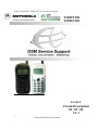
1
T200 / T2688
Level 1 & 2
Service Manual
Rev 1.2
T200 / T2688
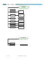
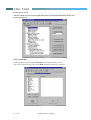
CONTENTS
Page Number
SECTION 1: GENERAL
1.1
1.2
1.3
Introduction
Motorola service policy for T200 in warranty
General Safety Information
v
vi
vii
SECTION 2: T200 DESCRIPTION
2.1
2.2
2.3
2.4
2.5
Specifications of T200
T200 Overview
Connector Pinout
Talk time, Weight and Volume Matrix
Battery Charging Times
2
3
6
6
8
SECTION 3: FEATURE LIST
3.1
List of Features available
9
3.2
3.3
3.4
3.5
3.6
3.7
3.8
3.9
3.10
Menu
Phone Book
Messages
Call Services
Phone Settings
Networks
Security
Audio Settings
Tools
9
9
10
11
12
12
13
13
14
SECTION 4: DISASSEMBLY & PARTS
4.1
4.2
4.3
4.4
4.5
4.6
Dissasembly Introduction
Recommended Tools
Disassembly Procedure
Assembly procedure
Exploded Parts diagram
Part Numbers
16
16
16
16
19
20
SECTION 5: SIM CARDS AND SECURITY
5.1
5.2
5.3
5.4
5.5
ii
of 51
Manual test mode
Live Sim Card
Personality Transfer
GSM Test Command
Identity and Security
42
42
42
44
45
GSM Field Service Support
T200 / T2688
SECTION 6: REPAIR & TEST PROCEDURES
6.1
6.2
6.3
6.4
6.5
6.6
Repair introduction
Mechanical repairs
Basic modular troubleshooting
Software Upgrade
Flexing
Testing on DM Tools
26
26
26
28
28
29
SECTION 7: ACCESSORIES
7.1
Accessory Introduction
35
SECTION 8: SALES MODELS
8.1
Sales Models Numbers
37
SECTION 9: GLOSSARY OF TERMS
9.1
iii
of 51
List of Abbreviations
41
GSM Field Service Support
T200 / T2688
SECTION 1: GENERAL
iv
of 51
GSM Field Service Support
T200 / T2688
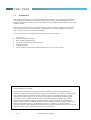
1.1
Introduction
This manual is intended for use by technicians familiar with similar types of equipment. It contains all
service information required for the equipment described and is current as of the printing date. This
manual is intended for use with the T200. The T200 is electrically and physically identical to the Asian
model the T2688.
The scope of this document is to provide the reader with basic information relating to the T200, and
also to provide procedures and processes for repairing the units up to and including Level 2 repair.
That is a repair that does not involve any soldering.
Level 1 and 2 repairs involve the following activities that can be carried out: •
•
•
•
•
•
•
Unit swap out
Repairing of mechanical faults
Basic modular troubleshooting
Testing and verification of unit functionality
Upgrading software
Flexing of product
Initiate warranty claims and send faulty modules to Level 3 or 4 repair centres.
Computer Software Copyrights
The Motorola products described in this instruction manual may include copyrighted Motorola
computer programs stored in semi-conductor memories or other media. Laws in the United States and
other countries preserve for Motorola certain exclusive rights for copyrighted computer programs,
including the exclusive right to copy or reproduce in any form the copyrighted computer program.
Accordingly, any copyrighted Motorola computer programs contained in the Motorola products
described in this instruction manual may not be copied or reproduced in any manner without the
express written permission of Motorola. Furthermore, the purchase of Motorola products shall not be
deemed to grant either directly or by implication, estoppel, or otherwise, any license under the
copyrights, patents or patent applications of Motorola, except for the normal non-exclusive, royalty free
license to use that arises by operation of law in the sale of a product.
v
of 51
GSM Field Service Support
T200 / T2688
1.2
Motorola Service Policy for T200 in warranty
1.2.1
Warranty:
Product will be sold with the standard 12 months warranty terms and conditions. Accidental damage
misuse, retailers extended warranties will not be supported under warranty. Non warranty repairs will
be available at agreed fixed repair prices.
Proof of purchase will be required to validate warranty claims.
1.2.2
Out of Box Failure Policy
The standard OOB failure criteria will apply. Customer units that fail very early on, after date of sale,
are to be returned to Manufacturing for root cause analysis, to guard against epidemic criteria.
Manufacturing to bear the costs of early life failure.
1.2.3
Product Support
Customers original units will be repaired but not refurbished as standard. Appointed Motorola Service
Hubs will perform warranty and non-warranty field service for level 2 (assemblies) and level 3 (limited
PCB component). The Motorola HTC centres will perform level 4 (full component) repairs.
1.2.4
Customer Support:
This will be available through dedicated Call Centres and In Country Help Desks.
Product Service training should be arranged through the local Motorola Support Centre.
1.2.5
Replacement Parts Ordering
Only centres authorized to carry out repairs will be able to purchase spare parts. Orders for spare parts
from Hub’s and Hi-Tech Centres should be placed with the regional Motorola Parts Distribution
Centre.
vi
of 51
GSM Field Service Support
T200 / T2688
1.3
General Safety Information
1.3.1 Portable Operation
• DO NOT hold the radio so that the antenna is very close to, or touching, exposed parts of the body,
especially the face or eyes whilst transmitting. The radio will perform best if it is held in the same
manner as you would hold a ‘land’ telephone handset, with the antenna angled up and over your
shoulder.
•
DO NOT operate the portable phone in an aircraft. Switch off your telephone. The use of a cellular
telephone in an aircraft may be dangerous to the operation of the aircraft, disruption of the Cellular
Network may occur, and is illegal. Failure to observe this instruction may lead to a suspension or
denial of Cellular Telephone Service to the offender, or legal action, or both.
1.3.2 Mobile/Portable Operation - Telephone use in Vehicles:
• All equipment must be properly grounded according to installation instructions for safe operation.
•
Users are advised to turn off their equipment when at a refueling point.
•
Safety is every driver’s responsibility. Cellular telephones should only be used in situations in
which the driver considers it safe to do so.
1.3.3 General
• DO NOT allow children to play with any radio equipment containing a transmitter.
•
DO NOT operate this equipment near electrical blasting caps or in an explosive atmosphere.
Mobile Telephones are, under certain conditions, capable of interfering with blasting operations.
When you are in the vicinity of such work, look out for and observe signs cautioning against
mobile radio transmission. If transmission is prohibited, you must turn off your mobile telephone
to prevent any transmission.
In standby mode the mobile telephone will automatically transmit to acknowledge a call if it is not
turned off.
•
Refer to the appropriate section of the product user manual for additional pertinent safety
information
•
All equipment should be serviced only by a Motorola qualified technician.
vii
of 51
GSM Field Service Support
T200 / T2688
SECTION 2:
T200
DESCRIPTION
1
of 51
GSM Field Service Support
T200 / T2688
2.1
Specifications of T200
General
Function
Frequency Range GSM
Frequency Range DCS
Channel Spacing
Channels
Modulation
Transmitter Phase Accuracy
Duplex Spacing
Frequency Stability
Operating Voltage
Transmit Current
Stand-by Current
Dimensions
Size (Volume)
Weight
Temperature Range
Transmitter
Function
RF Power Output
Output Impedance
Spurious Emissions
Receiver
Function
RF Level
RX bit error rate (100 k bits)
Channel Hop Time
Time to Camp
Speech Coding
Function
Speech Coding Type
Bit Rate
Frame Duration
Block Length
Classes
Bit Rate with FEC Encoding
2
of 51
Specification
890-915 MHz TX
915-960 MHz RX
1710-1785 MHz Tx
1805-1880 MHz Rx
200 kHz
124GSM/374 DCS carriers with 8 channels per carrier
GMSK at BT = 0.3
5 Degrees RMS, 20 Degrees peak
45 MHz GSM 95MHz DCS
+ 0.10 ppm of the (Uplink TX)
Battery Operating Voltage 2.7V – 4.2V (Li-Ion)
3.3V – 4.2V (NiMH)
Typically 250 ma avg, 1.0A peak
Typically 7.0 ma (DRX2)
112mm x 46mm x 18.5mm
78cc
90g with Battery
-20C to +55C
Specification
33 dBm + 2dB GSM/ 30 dBm + 2 dB DCS
50 ohms (nominal)
-36 dBm from 0.1 to 1 Ghz
-30 dBm from 1 to 4 Ghz
Specification
<-120 dBm GSM <-100 dBm DCS
< 2%
500 microseconds
Approximately 5-10 seconds
Specification
Regular Pulse Excitation / Linear Predictive Coding with Long
Term Prediction. (RPE LPC with LTP).
13.0 k bps
20 ms
260 bits
Class 1 bits = 182 bits. Class 2 bits = 78 bits
22.8 k bps
GSM Field Service Support
T200 / T2688
2.2
T200 Overview
The T200 is of the Dual Band technology range allowing roaming using the GSM 900 / 1800 bands.
The unit is an OEM product, and is the same product, mechanicaly and physically as the Asian T2688.
The unit will still be marketed within the Talkabout brand;
TalkAbout positioning statement:
“For those who want to stay in touch with friends and family within their busy lives, Motorola provides
mobile communications products that provide the peace of mind of staying connected to those
important to you, even when you’re apart, with hassle free features designed specifically for personal
connections.”
The following are a few of the main selling features that will be included with the unit.
•
•
•
•
•
•
•
•
•
•
•
•
•
•
•
•
•
New, slim and light form factor
SMS arriving indication
SMS overflow indication
Voice Mail arriving indication
SMS Cell Broadcast
CLI presentation
Date and time stamp for last 10 calls
USSD MO and Network Originated ALS
Calendar
Vibrator
Phone book holds 100 entries in memory and another 120 in the SIM Card
New animatated graphics
Calender & Calculator functions
VibracallTM
WAP 1.1. compliant
Calling Name Presentation
New Ringer Tones
Phase 2 USSD (Unstructured Supplementary Services Data) – This is an application whereby
pressing a certain key or combination of keys whilst in idle mode ie not in a call can access certain
network functions such as helplines etc...
•
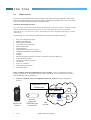
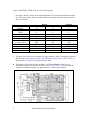
WAP 1.1 Compliancy (Wireless Application Protocol) - WAP 1.1 Wireless Application
Protocol
Simplified WAP
Architecture
‘The Internet’
Content Servers
Phone with
browser
3
of 51
Wireless
connection
(GSM Data call
is preferred)
WAP
Gateway
ISP
account
GSM Field Service Support
T200 / T2688
•
In the WAP environment this is how the access is made.
1. The request for information is made in WML (Wireless Markup Language) derived from HTML.
2. Request is passed to WAP Gateway, which retrieves the information from the server in standard
HTML (which is then filtered to WML) or if available WML format.
3. The information is then passed the cellular user, via the cellular network provider.
•
There will be 5 Data parameters that the user will be able to edit:
-Baud rate - between 2400 and 14400
-Idle time out
-Line type
-Phone Number
-Connection type
•
For image download, the bitmap image will be downloaded as text and if the image is larger than
the screen then only part of the image will be displayed
• Ways to access Browser - Quick access key and Feature Menu
During browser mode, if incoming call is received then the browser will be paused with the user having
the option to resume after the call.
Calling Name Presentation - This is an improvement on the existing name presentation.
• At present name from phone book is displayed by comparing last 8 digits of Number
• New feature will show name as sent by the network. This is up to 80 characters, but will be
shortened to 12 for the phonebook.
• This functionality must be subscribed to with network.
• Caller can restrict this
• On call arrival phone Number is compared to phonebook if match is found but name is not
allocated then callers name will be stored.(However if there is any text against that number it will
not be overwritten)
Display Animation - Aimed at physically showing the customer is executing commands.
Existing animations are for Power up and Down sequences.
• New animations • Incoming / sending call
• Incoming / sending SMS
• WAP Browsing
Call Divert Interrogation - This function is just a more accurate way of ensuring that the caller is
diverted to the correct number, this is mainly achieved through the co-operation of the network
providers.
Connectivity – The t200 supports Windows 95 / 98 / NT in data service. No PCMCIA card is required
4
of 51
GSM Field Service Support
T200 / T2688
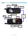
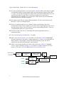
Lens w/
Talkabout
logo
Fig 2.1 Mechanical
pictorial Overview
Menu
access key
Microphone
Socket
Speaker Ports
Antenna
Volume
Keys
Screw
Locations
Lanyard
Loop
Battery
Contacts
5
of 51
SIM
Contacts
GSM Field Service Support
SIM
Retaining
slide
Accessory
and
Charger
Port
T200 / T2688
2.3 Connector Pinouts
• I06
• CHGERP
• GND
14
1
Charger Socket Pin Layout
1.Ext AUD MIC IN / JTAG TMS Use
3.GND / JTAG TMK Use
5.RS232 – DSR
7.RS232_TXD
9.DATA ID
11.IOPN11 – EXT. Power
13.ACCIN
2.4
2.JTAG TRST Use
4.Auxiliary Audio Out / JTAG TDI
6.RS232_RXD
8.RS232 - DTR
10.I06 / JTAG TDO Use
12.ACCID – Accessory ID
14.GND
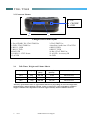
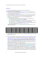
Talk Times, Weight and Volume Matrix
Volume (cc)
Weight (g)
Talk Time
(min)*
Standby Time
(hours)*
with Battery
78 cc
90 g
152-376
70-92
600 mAh LiIon
87cc
104g
164-408
76-99
650mAh Ni MH
86cc
107g
228-565
105-138
900 mAh LiIon
All battery performance times are approximate and will vary depending on network configuration,
band and status, and the functions selected. Times are quoted as a range from DRX=2 to DRX=9.
Support of DTX mode is dependent on network support and may not be available in all areas.
6
of 51
GSM Field Service Support
T200 / T2688
2.5
Battery Charging Times
Identical to Leap, maximum charge times shown.
Charge time with Switch
Battery
Mode Travel charger to 95%
7
Charge time with Linear
Travel charger to 95%
600 mAh LiIon
95 minutes
160 minutes
650mAh Ni MH
175 minutes
210 minutes
900 mAh LiIon
220 minutes
260 minutes
of 51
GSM Field Service Support
T200 / T2688
SECTION 3: FEATURE LIST
8
of 51
GSM Field Service Support
T200 / T2688
3.1
List of Features Available
Below is the list of Menu functions available at present. Pressing the following key can access the
menu option:
Menu
1st Generation Menu
Phone Book
Messages
Call
Services
Phone
Settings
Network
Security
Audio
Settings
Tools
nd
2 Generation Menu
3rd Generation Menu
4th Generation Menu
Th Generation Menu
6th Generation Menu
PHONE BOOK
Dialed
Last Number
Find Record
Name
1.Send
2.Edit
3.Delete
4.Move
Received
Missed
Delete All
Add Record
Delete
1.By Name
2.Delete All
Memory
1.SIM
2.Phone
Own Number
9
of 51
GSM Field Service Support
1.Dialed
2.Received
3.Missed
4.All
1.Delete all?
T200 / T2688
MESSAGES
Inbox
New Message
Outbox
Voicemail
Settings
Delete All
Topics
Route Center
Valid Period
1….1 Hour
2….6 Hours
3….12 Hours
4….1 day
5….1 Week
Reply path
1.On
2.Off
Notification
1.On
2.Off
Alert Beep
1.On
2.Off
Format
of 51
1.English
↓
16.Chinese
Language
Voice Mail
10
1.On
2.Off
Receive
Broadcast
GSM Field Service Support
1. Text
2. Paging
3. E-mail
4. Fax
5. Voice
6. Ermes
7. Telex
8. Grp4 Fax
T200 / T2688
CALL
SERVICES
Call Divert
Call Barring
Divert Voice
When Busy
All Outgoing
If No Reply
Number
Int’l Out
Unreachable
message
Int’l Exc. Home
Number
Divert Cond.
All Incoming
message
Divert Fax
message
Cancel All
Cancel All
Activate
message
Cancel
Status
Call Record
Last
1.Time
2.Cost
Call
All Calls
1.Time
2.Cost
3.Clear Time
4.Clear Cost
Call Rate
1.Currency
2.Charge Unit
Cost Limit
11
of 51
Line in Use
1. Line 1
2. Line 2
Next Call
1. Voice
2. Data
3. Fax
1.Activate
2.Cancel
Divert Data
In when Roam
Call Waiting
1.Activate
2.Cancel
3.Status
GSM Field Service Support
Cancel All?
T200 / T2688
PHONE
SETTINGS
Backlight
Auto Redial
1.Automatic
2.Prompt
3.Off
Answer by
1.Auto
2.Any Key
3.Send Key
Key Lock
Confirm?
Language
1.English
↓
3.Indonesian
Time Alert
1.On
2.Off
Restore
Phone Code?
Display
1.On
2.Animation 1
3.Animation 2
NETWORKS
Automatic
Manual
12
of 51
1.Available Networks
GSM Field Service Support
T200 / T2688
=
SECURITY
Code Status
Pin Code
Change Code
Pin Code
PIN 2
1.On
2.Off
Enter Code
Phone Code
Network Code
Fixed Dial
SIM Lock
Enter Password
View
Set Status
1.On
2.Off
Modify
Enter PIN 2
Set Status
1.On
2.Off
Change Code
Unlock code
AUDIO
SETTINGS
Ring Volume
Ring Type
Keypad Tone
Alarm Type
13
of 51
1.Ring 1
↓
6.Melody 1
↓
18.Melody 13
19.Vibrate
20.Vib → Ring
1.On
2.Off
1.Ring 1
↓
6.Melody 1
↓
18.Melody 13
19.Vibrate
20.Vib → Ring
GSM Field Service Support
T200 / T2688
TOOLS
Set Alarm
Set Time
1.On
2.Off
1.On
2.Off
Calender
Calculator
14
of 51
GSM Field Service Support
T200 / T2688
SECTION 4: DISASSEMBLY &
PARTS
15
of 51
GSM Field Service Support
T200 / T2688
4.1 Disassembly Introduction
The T200 is held together by 4 screws. 1 of these screws should be placed under the warranty seal, on
the RH side of the phone rear facing towards you, antenna up).
Ensure that a properly grounded high impedance conductive wrist strap is used whilst performing any
tasks during the disassembly and assembly of the unit
Avoid stressing the plastics in any way to avoid damage to either the plastics or internal components.
!! CAUTION !!
Many of the intergrated devices used in this equipment are vulnerable to damage from
electro-static charges. Ensure that adequate static protection is in place when handling,
shipping and servicing the internal components of this equipment.
4.2
Recommended Tools
The following tools are recommended for use during the assembly / disassembly of the T200.
•
Anti-static Mat Kit - 0180386A82, includes:
Antistatic mat 66-80387A95
Ground Cord 66-80334B36
Wrist Band 42-80385A59
•
•
Plastic Bladed Tool SLN7223A
T6 Torx Driver
4.3
Disassembly Procedure
The following set of diagrams will demonstrate the correct sequence and action required to disassemble
the T200
The use of the exploded diagram on pages 19 may be of some assistance for part recognition.
4.4
Assembly Procedure
Once the unit is disassembled and the repair is carried out, the unit must then be reassembled, this is
carried out in the exact reverse order as the disassembly. Although the housings are put back together
parrallel to each other not ‘hinged’ apart as in disassembly.
16
of 51
GSM Field Service Support
T200 / T2688
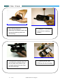
1. Turn off the telephone.
s
2. Slide down the battery latch, and
remove the battery pack from
the housing.
4. Unclip the 2 snap fits from the
left and right hand sides of the
unit and separate the rear from
the front housings.
17
of 51
GSM Field Service Support
3. Using a T5 Torx driver
remove the 4 retaining
screws.
5. Carefully lift the main
PCB from the front housing
T200 / T2688
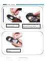
6. Insert the pointed end of plastic tool
below speaker and pull upwards.
Replace with new speaker after removal.
5. Remove Volume buttons
by pulling upwards.
9. Remove keypad from front
housing.
18
of 51
GSM Field Service Support
T200 / T2688
4.5
19
Exploded Parts Diagram
of 51
GSM Field Service Support
T200 / T2688
4.6 Part Numbers
*For Part numbers of other variants please consult Level 1&2 parts list)
Item
1.
2.
3.
4.
5.
6.
7.
8.
9.
10.
11.
12.
13.
14.
15.
16.
17.
18.
19.
20.
21.
22.
23.
24.
25.
26.
27.
28.
29.
30.
Part number
20.F0075.014
22.10128.006
22.80019.051
23.40046.001
23.60016.041
23.42007.031
25.90012.001
34.G0110.001
34.G0510.002
42.G0102.003
42.G0101.001
47.G0101.001
47.G0101.011
47.G0104.001
47.G0109.001
47.G0105.001
56.07249.071
60.G0105.001
60.G0109.003
60.G0108.003
60.G0108.021
60.G0108.011
60.G0108.041
60.G0108.051
60.G0108.061
60.G0108.071
86.1A52P.3R5
55.G0501.006
50.25001.021
90.25030.001
Description
System connector
SIM card connector
Vibrator motor
Speaker
Buzzer
Microphone
Antenna
Holder vibrator
Dome switches
LCD Holder
LCD cover
Keypad
Keypad (Chinese)
Microphone holder
Buzzer cap
Speaker cushion
LCD module
Volume-key switch
Lower case
Upper case(Blank)
Upper case(Yellow)
Upper case(Red)
Upper case(Blue)
Upper case(Silver)
Upper case(Titanium)
Upper case(Radar Blue)
Screw M1.6x6.5L
Main board (PCB)
RF cable
Downloader + cable
* The numbers on this part list to not correspond with the part
numbers on the exploded diagram.
20
of 51
GSM Field Service Support
T200 / T2688
SECTION 5: SIM CARDS AND
SECURITY
21
of 51
GSM Field Service Support
T200 / T2688
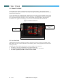
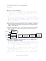
5.1 Manual Test Mode
The GSM Motorola T200 is equipped with a manual test mode capability. This capability allows
service personnel to take control of the unit, and by entering certain keypad commands, make the unit
performs desired functions.
To enter the manual test command mode, a GSM / DCS test sim (Part No 8102430Z04) must be used.
The test sim is inserted into the SIM slot beneath the battery (See figure 6.1), the battery should then
be re-inserted and the unit powered on. The # button should then be pressed for approximatly 3
second until ‘test’ appears on the display, and the correct commands must then be followed.
Figure 6.1 SIM Card insertion
SIM Retaining
slide
SIM Card
Slot
5.2 Live Sim Card
A SIM (Subscriber Identity module) card will be required to access the existing local GSM / DCS /
PCS cellular network, or remote networks when travelling. (If the roaming agreement has been made
with the provider.)
The SIM card contains all the data necessary to access GSM services, and also:
• The ability to store user information such as phone numbers etc…
• All information required by the network provider to provide use to the network
• For WAP Capability the SIM card must be Data enabled
22
of 51
GSM Field Service Support
T200 / T2688
5.4
GSM Test Commands
This is a list of Level 1 and 2 Manaul Test commands available to the T2688 / T200
GSM Test Commands
1)*#300# OK
List the Software and Hard ware version
2)*#301# OK
Full Keypads functional Test
3)*#307# OK
Engineering Test Mode
4)*#402# OK
Adjust Display Intensity/ Contrast
5)*#403# OK
List the Manufacturing Informations
6)1998 0722OKMaster Unlock code for Phone and Sim Lock
7)*#302# OK
Acoustic test*
1. Greeting
2. Main VlmGain
3. Input Cal
4. Output Cal
5. Side In Gain
6. Vox Gain
7. Min Mic Engy
8. More
(a) In vlm Gain
(b) Aux Vlm Gain
(c) Silence Prd
(d) Supp Prd
(e) In Volume
(f) Out Volume
(g) Icon
(h) Image
(i) Animation
8)#303# OK
Settings Saved*
9)#400# OK
ADC, Cal val*
•
•
Use with care - Contains Calibration factors
Please see DM Tools section for other test features.
23
of 51
GSM Field Service Support
T200 / T2688
5.5
Identity and Security
Each Motorola GSM Cellular Cassette will be labelled with various number configurations. The
following information describes what these configurations mean.
MSN
The mechanical Serial Number (MSN) is an individual unit identity number and will remain with the
unit throughout the life of the unit.
The MSN can be used to log and track a unit on Motorola’s EPPRS system.
The MSN is divided into 4 sections.
MSN 10 Digits
3 digits
APC
Account Product Code
I.e. Startac 130
1 digit
DC
Distribution Center
I.e. Easter Inch
2 digits
DC
4 digits
SNR
Date Code: Year and
Month of Shipment
Units individual serial
number
Figure 5.2 MSN label breakdown
IMEI
The International Mobile station Equipment Identity (IMEI) number is an individual number unique to
the PCB and is stored within the unit’s memory. The following figure gives a description of the make
up of this number.
IMEI 15 Digits
Type Approval code
6 digits
2 digits
6 digits
1 digits
TAC
FAC
SNR
IU
Distribution Center
factory code
Individual PCB Serial
Number
Internal use – spare
digits
Figure 5.3 IMEI label breakdown
Some other label number configurations that will be present will be: XCVR NUMBER: Identifies type of product. i.e. T200 (Usually SWF / SUG number)
PACKAGE / MODEL NUMBER: Determines type of equipment, mode in which it was shipped and
language with which it was shipped. e.g SA1255XXXXX
24
of 51
GSM Field Service Support
T200 / T2688
SECTION 6: REPAIR AND TEST
PROCEDURES
25
of 51
GSM Field Service Support
T200 / T2688
6.1 Repair Introduction
The T200 is divided into 2 main sections when it comes to part replacability: The housings which
contains the speaker, keypad and the Volume Buttons , the main PCB which contains RF / Logic
circuitry and the keypad interface and the display. If the RF / Logic board is required to be changed
then a full service tranceiver should be ordered as there is no replacement PCB available.
6.2
Mechanical repairs
Assembly replacement level troubleshooting and repair of the T200 is limited to isolation and
replacement of the main mechanical parts only (See Exploded parts diagram and associated parts list
p19)
6.3
Basic Modular Troubleshooting
The troubleshooting information in Table 2 shows some typical malfunction symptoms, and for the
corresponding verification and repair procedures refer to the disassembly instructions located in the
disassembly section of this manual. (Section 4).
NOTE
26
of 51
Defective Logic/RF assemblies must be replaced
with pre-tested, pre-phased assemblies
GSM Field Service Support
T200 / T2688
Repair Chart
Table 2. GSM T200 Cellular Telephone: Troubleshooting and Repair Chart. (Assembly Replacement
Level).
SYMPTOM
Personal telephone will not turn on or
stay on
PROBABLE CAUSE
VERIFICATION AND
REMEDY
a) Battery pack either
discharged or defective
Measure battery. If the battery voltage is <3.6V dc,
recharge the battery using the appropriate battery
charger. If the battery will not recharge, replace the
battery.
If battery is not at fault, proceed to b.
b) Battery connectors open
or misaligned.
Visually inspect the 4 battery connectors on both the
battery assembly and the portable telephone.
If necessary, replace the battery. If battery is not at
fault, proceed to c
c) Logic/RF Board
Assembly
Defective.
Remove the Logic/RF Assembly. Substitute a known
good assembly and temporarily reassemble the unit.
Depress the PWR button; if unit turns on and stays
on, disconnect the dc power source replace the faulty
unit.(see personality transfer).
a) Antenna is defective
Check to make sure that the antenna pin is properly
connected into the Logic/ RF assembly. If OK,
substitute a known good antenna and test in a call. If
the fault is still present, proceed to b.
b) Logic/RF Board
Assembly
Defective.
Replace Logic/RF Assembly (refer to symptom 1c).
Verify that fault has been cleared and replace faulty
unit.
3. Display is erratic, or provides
Partial or no display.
a) Logic/RF Board
Assembly
Defective.
Replace Logic/RF Assembly (refer to symptom 1c).
Verify that fault has been cleared and replace faulty
unit.
4. Incoming call alert transducer audio
distorted or volume is too low.
a) Logic/RF Board
Assembly
Defective.
Replace Logic/RF Assembly (refer to symptom 1c).
Verify that fault has been cleared and replace faulty
unit.
5. Personal telephone transmit audio is
weak, (usually indicated by called parties
complaining of difficulty in hearing
voice from personal phone).
6. Personal telephone receive audio is
weak and/or distorted. (From speaker)
a) Logic/RF Board
Assembly
Defective.
Replace Logic/RF Assembly (refer to symptom 1c).
Verify that fault has been cleared and replace faulty
unit.
a) Connections to/from
speaker and Logic/RF
Circuit board defective.
Gain access to Logic/RF board as described in the
DISASSEMBLY instructions in this manual. Check
contact springs on the Logic/RF circuit board. Clean
pads if necessary. If spring is at fault proceed to d. If
connection is not at fault, Proceed to b.
Remove speaker from front housing and insert
known good speaker. Place a call and verify
improvement in earpiece audio. If better, reassemble
the phone with the good speaker. If it was no better
then proceed to c.
2. Personal telephone exhibits poor
reception and/or erratic operation
(such as calls frequently dropping,
Weak and/or distorted audio, etc.).
b) Earpiece Speaker
defective.
c) Antenna assembly is
defective.
d) Logic/RF Board
Assembly
Defective.
27
of 51
Check to make sure that the antenna pin is properly
connected into the Logic/ RF assembly. If OK,
substitute a known good antenna and test in a call. If
the fault is still present, proceed to d.
Replace Logic/RF Assembly (refer to symptom 1c).
Verify that fault has been cleared and replace faulty
unit.
GSM Field Service Support
T200 / T2688
SYMPTOM
7. Personal telephone will not
recognize/accept SIM card
PROBABLE CAUSE
a) SIM card defective
b) SIM retention latch
defective
9. Internal Charger not working
c) Logic/RF Board
Assembly
Defective.
a) Faulty Charger
10. Weak or No vibrate Function
b) Logic/RF Board
Assembly
Defective.
a) Defective Vibrate motor
b) Logic/RF Board
Assembly
Defective.
6.4
VERIFICATION AND
REMEDY
Initially check that the contacts on the card are not
dirty and that the SIM retention latch is pushed fully
across. Clean if necessary, and check if fault has
been eliminated. If the contacts are clean, insert a
Known good SIM card into the portable telephone.
Power up the unit and confirm whether or not the
card has been accepted. If the fault no longer
Exists, the defective SIM card should be replaced. If
the SIM card is not at fault, proceed to b.
Remove rear housing as per DISASSEMBLY
instructions and replace with known good rear
housing, ensure the latch is pushed fully across, if
unit now tests OK, replace faulty rear housing. If not
proceed to c)
Replace Logic/RF Assembly (refer to symptom 1c).
Verify that fault has been cleared and replace faulty
unit.
Attempt to charge unit with known good charger, if
OK replace charger. If fault still exists, proceed to b)
Replace Logic/RF Assembly (refer to symptom 1c).
Verify that fault has been cleared and replace faulty
unit.
Access Vibrate motor using DISASSEMBLY
procedure, unplug and replace vibrator with known
good assembly. If unit now vibrates OK, build unit
back up with good vibrator. If fault still exists
proceed to b)
Replace Logic/RF Assembly (refer to symptom 1c).
Verify that fault has been cleared and replace faulty
unit.
Software Upgrade
See DM Tool section
6.5
Flexing
See DM Tools section
28
of 51
GSM Field Service Support
T200 / T2688
6.6
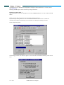
Testing on DM TOOLS
Below is the power up screen on selecting DM Tools.
File Types:
Boot file is of type .mot and the naming protocol is of the form r_amdt.mot
Flash file is of type .mot and the naming protocol is taken from the s/w version
As seen above 70131411.mot
Database file is a binary (.bin)type and the naming protocol is also derived from
The s/ware version e.g. 701314.bin
First select options from tool bar then:
Set comm port either 1 or 2 (the gray dot indicates selected port).
Set baud rate 19200 to allow flexing access.
Set eeprom mode default.
Remove charger jack from download box.
Note:
To upgrade the s/w from 701205 to 701214 you must use the database file, associated with the older
version (701205). So in the Choose Database File you would choose 701205.bin instead of 701214.bin
To then use flexing tools, the database should be changed to the later version, in this case 701214.bin
The software for the T205 is 7013xx and for the T200 it is 7012xx
The selection of the Boot file is as above
The Flash file is derived from the s/w version as above
29
of 51
GSM Field Service Support
T200 / T2688
The database file is a filename.bin configuration, and again is derived from the s/w version. (In this
case 701314.bin)
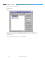
Selecting the Files option on the tool bar may change all the files.
Flashing Procedure STEP 1
After selecting the correct files, plug phone into cable but DO NOT power on. Then hit the download
button.
When you get to this point you have 10 seconds to power the phone on
If you don’t power the phone on in the 10 seconds then DM Tools will see this as a flash fail.
Assuming no problems the following screen should be seen during the flashing procedure
Screen dump during flash
The flashing procedure also flexes the phone. At the end of the download the following screen can be
seen.
30
of 51
GSM Field Service Support
T200 / T2688
Follow instruction’s above to flex phone.
Flexing Procedure
Select Service from tool bar and choose the Flex option to obtain the following screen.
The flex settings are loaded from a file with designation (.fle ) and is known as FlexOption Profile. The
load option is obtained by right clicking the mouse on the DM Tools’s window, and then selecting
Load from Profile.
The U.U.T. should be powered on first for all flexing operations
31
of 51
GSM Field Service Support
T200 / T2688
Flexing options screen.
*The flex options are password protected and can not be changed manually unless the key and
password are known.
TEST COMMANDS
Select View from tool bar and highlight MMI Test to obtain the following screen.
Then tick the appropriate test and press the MMI Test button and follow instructions.
32
of 51
GSM Field Service Support
T200 / T2688
SECTION 7: ACCESSORIES
33
of 51
GSM Field Service Support
T200 / T2688
7.1 Introduction: The following is a short description of accessories available for the T200 that
are currently available.
Switch mode Travel Charger
•
•
Input: 90-260V, varies by plug type for each country, AC
Output: 6V, 750 mA
Linear Travel Charger
•
Input: voltage and plug requirements per each
country, AC
Cigarette Charger
•
•
Input: 12-24V, DC
Output: 6V, 750 mA
Portable Hands-free
(plugs into butt plug)
Desktop charger base – conceptual design.
Picture
not
available
Picture
not
available
Simple car kit.
Data Cable
Switch mode and linear travel chargers with these plug types are required: US (without holes
in prongs for the PRC), UK, Euro, Aust/NZ, India.
34
of 51
GSM Field Service Support
T200 / T2688
SECTION 8: SALES MODEL
NUMBERS
35
of 51
GSM Field Service Support
T200 / T2688
8.1
Sales Model Numbers
Part Number of T200 with T-options
Country
Australia
Telstra
Australia
Optus
Australia
Vodafone
Australia
OneTel
Australia
Distributors
NZ
NZ
36
of 51
T-option
API p/n
Color
Moto p/n
Descripton
T948UB
99.G0521.BOF Copper Orange SA2143AE5B1 SA2143AE5B1,AU ORG
T948UB
99.G0521.BGF Misty Green
SA2143AF5B1 SA2143AF5B1,AU GRN
T948UB
99.G0521.BIF
SA2143AG5B1 SA2143AG5B1,AU ICE
T948UB
99.G0521.BBF Elec Blue
T948UC
99.G0521.COF Copper Orange SA2143AE5B1 SA2143AE5B1,AU ORG
T949UC
99.G0521.CGF Misty Green
SA2143AF5B1 SA2143AF5B1,AU GRN
T950UC
99.G0521.CIF
SA2143AG5B1 SA2143AG5B1,AU ICE
T951UC
99.G0521.CBF Elec Blue
T948UD
99.G0521.DOF Copper Orange SA2143AE5B1 SA2143AE5B1,AU ORG
T948UD
99.G0521.DGF Misty Green
SA2143AF5B1 SA2143AF5B1,AU GRN
T948UD
99.G0521.DIF
SA2143AG5B1 SA2143AG5B1,AU ICE
T948UD
99.G0521.DBF Elec Blue
T948UE
99.G0521.EOF Copper Orange SA2143AE5B1 SA2143AE5B1,AU ORG
T948UE
99.G0521.EGF Misty Green
SA2143AF5B1 SA2143AF5B1,AU GRN
T948UE
99.G0521.EIF
SA2143AG5B1 SA2143AG5B1,AU ICE
T948UE
99.G0521.EBF Elec Blue
T948UF
99.G0521.FOF Copper Orange SA2143AE5B1 SA2143AE5B1,AU ORG
T948UF
99.G0521.FGF Misty Green
SA2143AF5B1 SA2143AF5B1,AU GRN
T948UF
99.G0521.FIF
SA2143AG5B1 SA2143AG5B1,AU ICE
T948UF
99.G0521.FBF Elec Blue
T948UG
99.G0521.GOD Copper Orange SA2147AE5B1 SA2147AE5B1,NZ ORG
T948UG
99.G0521.GGD Misty Green
SA2147AF5B1 SA2147AF5B1,NZ GRN
T948UG
99.G0521.GID
SA2147AG5B1 SA2147AG5B1,NZ ICE
T948UG
99.G0521.GBD Elec Blue
T948UH
99.G0521.HOD Copper Orange SA2147AE5B1 SA2147AE5B1,NZ ORG
T948UH
99.G0521.HGD Misty Green
SA2147AF5B1 SA2147AF5B1,NZ GRN
T948UH
99.G0521.HID Teal Ice
SA2147AG5B1 SA2147AG5B1,NZ ICE
T948UH
99.G0521.HBD Elec Blue
SA2147AJ3B1 SA2147AJ3B1,NZ EBU
Teal Ice
Teal Ice
Teal Ice
Teal Ice
Teal Ice
Teal Ice
SA2143AJ3B1 SA2143AJ3B1,AU EBU
SA2143AJ3B1 SA2143AJ3B1,AU EBU
SA2143AJ3B1 SA2143AJ3B1,AU EBU
SA2143AJ3B1 SA2143AJ3B1,AU EBU
SA2143AJ3B1 SA2143AJ3B1,AU EBU
SA2147AJ3B1 SA2147AJ3B1,NZ EBU
GSM Field Service Support
T200 / T2688
Maly/SGP
Maly/SGP
Maly/SGP
Maly/SGP
Maly/SGP
Maly/SGP
Maly/SGP
Maly/SGP
37
of 51
T948UP
99.G0521.POH Copper Orange SA2150AE5B1 SA2150AE5B1,SG ORG
T948UP
99.G0521.PGH Misty Green
SA2150AF5B1 SA2150AF5B1,SG GRN
T948UP
99.G0521.PIH
SA2150AG5B1 SA2150AG5B1,SG ICE
T948UP
99.G0521.PBH Elec Blue
T948UQ
99.G0521.QOH Copper Orange SA2150AE5B1 SA2150AE5B1,SG ORG
T948UQ
99.G0521.QGH Misty Green
SA2150AF5B1 SA2150AF5B1,SG GRN
T948UQ
99.G0521.QIH Teal Ice
SA2150AG5B1 SA2150AG5B1,SG ICE
T948UQ
99.G0521.QBH Elec Blue
SA2150AJ3B1 SA2150AJ3B1,SG EBU
T948UR
99.G0521.ROH Copper Orange SA2150AE5B1 SA2150AE5B1,SG ORG
T948UR
99.G0521.RGH Misty Green
SA2150AF5B1 SA2150AF5B1,SG GRN
T948UR
99.G0521.RIH
SA2150AG5B1 SA2150AG5B1,SG ICE
T948UR
99.G0521.RBH Elec Blue
T948US
99.G0521.SOH Copper Orange SA2150AE5B1 SA2150AE5B1,SG ORG
T948US
99.G0521.SGH Misty Green
SA2150AF5B1 SA2150AF5B1,SG GRN
T948US
99.G0521.SIH
SA2150AG5B1 SA2150AG5B1,SG ICE
T948US
99.G0521.SBH Elec Blue
T948UW
99.G0521.WOH Copper Orange SA2150AE5B1 SA2150AE5B1,SG ORG
T948UW
99.G0521.WGH Misty Green
SA2150AF5B1 SA2150AF5B1,SG GRN
T948UW
99.G0521.WIH Teal Ice
SA2150AG5B1 SA2150AG5B1,SG ICE
T948UW
99.G0521.WBH Elec Blue
SA2150AJ3B1 SA2150AJ3B1,SG EBU
T948UX
99.G0521.XOH Copper Orange SA2150AE5B1 SA2150AE5B1,SG ORG
T948UX
99.G0521.XGH Misty Green
SA2150AF5B1 SA2150AF5B1,SG GRN
T948UX
99.G0521.XIH Teal Ice
SA2150AG5B1 SA2150AG5B1,SG ICE
T948UX
99.G0521.XBH Elec Blue
SA2150AJ3B1 SA2150AJ3B1,SG EBU
T948UY
99.G0521.YOH Copper Orange SA2150AE5B1 SA2150AE5B1,SG ORG
T948UY
99.G0521.YGH Misty Green
SA2150AF5B1 SA2150AF5B1,SG GRN
T948UY
99.G0521.YIH Teal Ice
SA2150AG5B1 SA2150AG5B1,SG ICE
T948UY
99.G0521.YBH Elec Blue
SA2150AJ3B1 SA2150AJ3B1,SG EBU
T948UZ
99.G0521.ZOH Copper Orange SA2150AE5B1 SA2150AE5B1,SG ORG
T948UZ
99.G0521.ZGH Misty Green
SA2150AF5B1 SA2150AF5B1,SG GRN
T948UZ
99.G0521.ZIH
SA2150AG5B1 SA2150AG5B1,SG ICE
T948UZ
99.G0521.ZBH Elec Blue
Teal Ice
Teal Ice
Teal Ice
Teal Ice
SA2150AJ3B1 SA2150AJ3B1,SG EBU
SA2150AJ3B1 SA2150AJ3B1,SG EBU
SA2150AJ3B1 SA2150AJ3B1,SG EBU
SA2150AJ3B1 SA2150AJ3B1,SG EBU
GSM Field Service Support
T200 / T2688
Part Number of T200 with SIM Lock
Country
Thailand
Thailand
Philippines
Philippines
Philippines
Philippines
Philippines
Philippines
38
of 51
T-option
API p/n
Color
Moto p/n
Descripton
AIS/DPC
99.G0521.AOB Copper Orange SA2145AE5X3
SA2145AE5X3,THA ORG
AIS/DPC
99.G0521.AGB Misty Green
SA2145AF5X3
SA2145AF5X3,THA GRN
AIS/DPC
99.G0521.AIB
SA2145AG5X3
SA2145AG5X3,THA ICE
AIS/DPC
99.G0521.ABB Elec Blue
SA2145AJ3X3
SA2145AJ3X3,THA EBU
TAC
99.G0521.BOB Copper Orange SA2151AE5X3
SA2151AE5X3,THA ORG
TAC
99.G0521.BGB Misty Green
SA2151AF5X3
SA2151AF5X3,THA GRN
TAC
99.G0521.BIB
SA2151AG5X3
SA2151AG5X3,THA ICE
TAC
99.G0521.BBB Elec Blue
SA2151AJ3X3
SA2151AJ3X3,THA EBU
T948UJ
99.G0521.JOC Copper Orange SA2148AE5B1
SA2148AE5B1,PHI ORG
T948UJ
99.G0521.JGC
Misty Green
SA2148AF5B1
SA2148AF5B1,PHI GRN
T948UJ
99.G0521.JIC
Teal Ice
SA2148AG5B1
SA2148AG5B1,PHI ICE
T948UJ
99.G0521.JBC
Elec Blue
SA2148AJ3B1
SA2148AJ3B1,PHI EBU
T948UK
99.G0521.KOC Copper Orange SA2148AE5B1
SA2148AE5B1,PHI ORG
T948UK
99.G0521.KGC Misty Green
SA2148AF5B1
SA2148AF5B1,PHI GRN
T948UK
99.G0521.KIC
SA2148AG5B1
SA2148AG5B1,PHI ICE
T948UK
99.G0521.KBC Elec Blue
SA2148AJ3B1
SA2148AJ3B1,PHI EBU
T948UL
99.G0521.LOC Copper Orange SA2148AE5B1
SA2148AE5B1,PHI ORG
T948UL
99.G0521.LGC Misty Green
SA2148AF5B1
SA2148AF5B1,PHI GRN
T948UL
99.G0521.LIC
SA2148AG5B1
SA2148AG5B1,PHI ICE
T948UL
99.G0521.LBC Elec Blue
SA2148AJ3B1
SA2148AJ3B1,PHI EBU
T948UM
99.G0521.MOC Copper Orange SA2148AE5B1
SA2148AE5B1,PHI ORG
T948UM
99.G0521.MGC Misty Green
SA2148AF5B1
SA2148AF5B1,PHI GRN
T948UM
99.G0521.MIC Teal Ice
SA2148AG5B1
SA2148AG5B1,PHI ICE
T948UM
99.G0521.MBC Elec Blue
SA2148AJ3B1
SA2148AJ3B1,PHI EBU
T948UN
99.G0521.NOC Copper Orange SA2148AE5B1
SA2148AE5B1,PHI ORG
T948UN
99.G0521.NGC Misty Green
SA2148AF5B1
SA2148AF5B1,PHI GRN
T948UN
99.G0521.NIC
SA2148AG5B1
SA2148AG5B1,PHI ICE
T948UN
99.G0521.NBC Elec Blue
SA2148AJ3B1
SA2148AJ3B1,PHI EBU
T948VD
99.G0521.VOC Copper Orange SA2148AE5B1
SA2148AE5B1,PHI ORG
T948VD
99.G0521.VGC Misty Green
SA2148AF5B1
SA2148AF5B1,PHI GRN
T948VD
99.G0521.VIC
SA2148AG5B1
SA2148AG5B1,PHI ICE
T948VD
99.G0521.VBC Elec Blue
SA2148AJ3B1
SA2148AJ3B1,PHI EBU
Teal Ice
Teal Ice
Teal Ice
Teal Ice
Teal Ice
Teal Ice
GSM Field Service Support
T200 / T2688
SECTION 9: GLOSSARY OF
TERMS
39
of 51
GSM Field Service Support
T200 / T2688
9.1 List of Abbreviations
Those marked ** are Motorola specific abbreviations.
µBGA
Micro Ball Grid Array
A Interface
A3
A5
A8
AB
A-bis
ACCH
ACSE
AGCH
AMPS
AOC
ARFCN
ARQ
ASIC
AUC
AUT (H)
Interface between MSC and BSS
Authentication algorithm
Stream cipher algorithm
ciphering key generating algorithm
Access Burst
Interface between BSC and BTS
Associated Control Channel
Association Control Service Element
Access Grant Channel
Advance Mobile Phone System
Advice of charge
Absolute Radio Frequency Channel Number
Automatic Request for retransmission
Application Specific Integrated Circuit
Authentication Center
Authentication
BA
BAIC
BAOC
BCC
BCCH
BCD
BGA
BCU
Bm
BN
BS
BSC
BSIC
BSS
BSSAP
BSSC
BSSMAP
BSSOMAP
BSU
BTS
BCCH Allocation
Barring of All Incoming Calls
barring of all Outgoing Calls
Base Transceiver Station (BTS) Color Code
Broadcast Control Channel
Binary Coded Decimal
Ball Grid Array
BTS Control Unit **
Full-rate traffic channel
Bit Number
Base Station
Base Station Controller
Base Transceiver Station Identity Code
Base Station System
BSS Application Part (DTAP and BSSMAP)
Base Station System Control Cabinet **
Base Station Systems Management Application Part
BSS Operation and Maintenance Application Part
Base Site Controller Unit **
Base Transceiver Station
CA
CBCH
cc
cc
CC
CCBS
CCH
CCCH
CDMA
CFS
CFU
CLIP
CLIR
CM
40
of 51
Call Allocation
Call Broadcast Channel
Call Control
Country Code
Cellular Cassette
Completion of Calls to Busy Subscribers
Control Channel
Common Control Channel
Code Division Multiple Access
Call Forwarding on mobile Subscriber busy
Call Forwarding Unconditional
Calling Line Identification Presentation
Calling Line Identification Restriction
Connection Management
GSM Field Service Support
T200 / T2688
COLP
COLR
CONF
Connected Line identification Presentation
Connected Line identification Restriction
Conference Call add on
CSPDN
CUG
CW
Circuit Switched Public Data Network
Closed User Group
Call Waiting
DB
DBS
DCCH
DET
DFE
DISC
DL
Dm
Dm
Dp
DRCU
DRX
DTAP
DTE
DTMF
DTX
Dummy Burst
Distributed Base Station **
Dedicated Control Channel
Detach
Decision Feedback Equalizer
Disconnect
Data Link (layer)
Control Channel (ISDN terminology applied to mobile service)
Signaling channel
Dialed Pulse
Diversity Radio Channel Unit**
Discontinuous Reception
Direct Transfer Application Part
Data Terminal Equipment
Dual Tone Multi-Frequency (tone signaling type)
Discontinuous Transmission
E
Eb/No
EC
Ec/No
EGSM
EFR
EIR
EIRP
EMC
EMX
ETSI
erlang
Energy per Bit/Noise floor
Echo Canceller
Ratio of energy per modulating bit to the noise spectral density
Extended Group special Mobile
Enhanced Full Rate
Equipment Identity Register
Effective Isotropic Radiated Power
Electromagnetic Compatibility
Electronic Mobile Exchange **
European Telecommunications Standards Institute
FACCH
FACCH/F
FACCH/H
FB
FCCH
FEC
FN
FR
FTAM
GCC
GMSC
GMSK
GSM
GSM MS
GSM PLMN
HANDO
HATIS
HDLC
HLR
HOLD
41
of 51
Fast Associated Control channel
Full rate Fast Associated Control channel
Half rate fast Associated Control channel
Frequency correction burst
Frequency Correction Channel
Forward Error Correction
Frame Number
Full Rate
File Transfer Access Management
Global Call Center
Gateway Mobile Services Switching Center
Gaussian Minimum Shift Keying
Group Special Mobile
GSM Mobile Station
GSM Public Land Mobile Network
Handover
Hearing Aid Telephone Interconnection System
High Level Data Link Control
Home Location Register
Call Hold (Supplementary Service)
GSM Field Service Support
T200 / T2688
HPLMN
HPU
HR
HSN
Home PLMN
Hand Portable Unit
Half Rate
Hopping Sequence Number
I
IA5
ID
IMEI
IMM
IMSI
IN
INDY
IrDA
ISC
ISU
ISDN
ISUP
IWF
Information (frames)
International Alphanumeric 5
Identification
International Mobile Equipment Identity
Immediate assignment message
International Mobile Subscriber Identity
Intelligent Network
Iridium 9500 handset
Infra Red Data Association
International Switching Center
Iridium Subscriber Unit
Integrated Services Digital Network
ISDN User Part
Interworking Function
Kc
Ki
ciphering Key
Individual subscriber authentication key
LAC
LAI
LAPB
LAPDm
Lm
LPC
LR
Location Area Code
Location Area Identification (Identity)
Link Access Procedure ‘B’ (balanced) channel
Link Access Procedure ‘DM’ (mobile ‘D’) channel
Traffic channel (with capacity lower than Bm)
Linear Predictive Code
Location Register
MA
MAH
MAI
MAIO
MAP
MCC
MCI
MD
ME
MF
MLSE
MM
MMI
MNC
MO
MO/PP
MoU
MRN
MS
MSC
MSCM
MSIN
MSISDN
MSRN
MT
MTP
MT/PP
Mobile Allocation
Mobile Access Hunting
Mobile Allocation Index
Mobile Allocation Index Offset
Mobile Application Part
Mobile Country Code
Malicious Call Identification
Mediation Device
Mobile Equipment
Multi-Frequency (tone signaling type)
Maximum Likelihood Sequence Estimator
Mobility Management
Man Machine Interface
Mobile Network Code
Mobile Originated
Mobile Originated Point to Point messages
Memorandum of Understanding
Mobile Roaming Number
Mobile Station
Mobile Services Switching Center
Mobile Station Class Mark
Mobile Station Identification Number
Mobile Station international ISDN number
Mobile Station Roaming Number
Mobile Termination
Message Transfer Part
Mobile Terminated Point to Point messages
42
of 51
GSM Field Service Support
T200 / T2688
NAMPS
NB
NE
NET
NM
NHC
North American-Advance Mobile Phone System
Normal Burst
Network Elements
Norme European de Telecommunications
Network Management
Network Management Center
O&M
OACSU
OCB
OMAP
OMC
OMCR
OMCS
OSI
Operations and Maintenance
Off Air Call Set-Up
Outgoing Calls Barred
Operations and Maintenance Application Part (previously was OAMP)
Operations and Maintenance Center
Operations and Maintenance Center -Radio Part
Operations and Maintenance Center -Switch Part
Open System Interconnection
PAD
PCH
PDN
PIN
PLMN
POTS
PSPDN
PSTN
PTO
Packet Assembly Disassembly facility
Paging Channel
Public Data Networks
Personal Identification Number
Public Land Mobile Network
Plain Old Telephone Service (basic telephone services)
Public Switched Packet Data Network
Public Switched Telephone
Public Telecommunications Operator
QOS
Quality of Service
RAB
RACH
RBDS
RBU
RCU
REC
REL
RELP-LTP
REQ
RFCH
RFN
RLP
ROSE
RXCDR
RXLEV
RXQUAL
SABM
SACCH
SAPI
SB
SC
SCCP
SCH
SCP
SDCCH
SDL
SFH
SIM
SMS
43
of 51
Random Access Burst
Random Access Channel
Remote BSS Diagnostic Subsystem **
Remote Base Station Unit (PCN) **
Radio Channel Unit **
Recommendation
Release
Regular Pulse Excitation - Long Term Prediction
Request
Radio Frequency Channel
Reduced TDMA Frame Number
Radio Link Protocol
Remote Operations Service Element (a CCITT specification for O&M)
Remote Transcoder Unit **
Received signal level
Received signal quality
Set Asynchronous Balance Model
Slow Associated Control Channel
Service Access Point Indicator (Identifier)
Synchronization Burst
Service Center
Signaling Connection Control Part
Synchronization Channel
Service Control Point - an intelligent network entity
Stand-alone Dedicated Control Channel
Specification Description Language
Slow Frequency Hopping
Subscriber Identity Module
Short Message Service
GSM Field Service Support
T200 / T2688
SMSCB
SND
SP
SRES
SS
SS
STP
Short Message Service Call Broadcast
SeND
Signaling Point
Signed RESponse (authentication)
Supplementary Service
System Simulator
Signaling Transfer Point
SYSGEN
SYStem GENeration
TA
TA
TCAP
TCH
TCH/F
TCH/FS
TCH/HS
TCP
TDMA
TE
TMN
TMSI
TN
TRX
TTY
TS
TUP
Terminal Adapter
Timing Advance
Transaction Capabilities Application Part
Traffic Channel
A full rate TCH
A full rate speech TCH
A half rate speech TCH
Transmission Control Protocol
Time Division Multiple Access
Terminal Equipment
Telecommunications Management Network
Temporary Mobile Subscriber Identity
Timeslot Number
Transceivers
TeleTYpe (refers to any terminal)
Time Slot
Telephone Users Part
UI
Um
USSD
Unnumbered Information frame
Air Interface
Unstructured Supplementary Services Data
VAD
VLR
VLSI
VPLMN
Voice Activity Detection
Visited Location Register
Very Large Scale Integration (IC)
Visited PLMN
XC
XCDR
Transcoder
Transcoder **
3PTY
Three party service
44
of 51
GSM Field Service Support
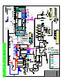
Topaz T2688/T200, T2988/T205 L3 Circuit Description
T2688/T200
T2988/T205
Level 3
Circuit Description
01 / 03 / 01
V1.3
1
Motorola Proprietary Information
Topaz T2688/T200, T2988/T205 L3 Circuit Description
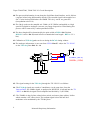
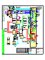
RECEIVE
1. Received GSM 900 frequency enters the unit at the Antenna ANT1
2. L501 / L502 / L503 provide matching
3. The signal then enters mechanical Auxiliary RF port U113. When a load (50? is
placed into the socket the RF will be diverted into or out of U113). This socket will
be used for phasing, testing purposes.
4. From U113 Pin 1 to RF Switch U501 Pin 9 (ANT), where through control voltages
the Rx path is isolated from the TX path. The following voltages control the RF
Switch: VC1 – VC4, which are all 0V or 3.6V Low or High respectively.
The controlling input signals are:
? BS (Band Select), this signal determines GSM (Logic 0) or DCS (Logic 1) –
2.8V (originates as BANDSW from Gemini Pin 65)
? PA_ON, this signal determines if the TX burst is on progress (for use with the
RF Switch only) – 2.8V (originates as TXPA from Gemini Pin 119)
? VBAT, is the battery voltage and supports both U502 which is the Logic control
for the RF switch and the inverter IC501 - 3.3V – 3.6V
Below are the states of VC1 – VC4 and the relative states of BS and PA_ON for
each of the 4 scenarios.
GSM RX
GSM TX
DCS RX
DCS TX
VC1
0V
3.6V
0V
0V
VC2
3.6V
0V
3.6V
3.6V
VC3
3.6V
3.6V
3.6V
0V
VC4
0V
0V
0V
3.6V
BS
0V
0V
2.8V
2.8V
PA_ON
0V
2.8V
0V
2.8V
5. The appropriate frequency is then fed out from U501 Pin 5 (GSM) GSM_RX or from
Pin 7 (DCS) DCS_RX.
6. The received frequency is then fed into a Dual Band select SAW (Standing Acoustic
Wave) filter U602 (Loss approximately 5dB). The GSM received frequency is then
applied to the base of Low Noise amplifier Q601, with input matching supplied by
C613 / L608 / C616 and the collector output matching elements supplied by C614 /
L607 / C606. The support voltage for Q601 and Q602 is from TX / RX IC U603 (see
Figure 1 for Block Schematic) Pin 3 (RFOUT ) and is 2.1V when active. The bias
voltage that is approximately 1.4V will be used to switch the correct LNA on or off
dependant upon band selected, or mode of operation.
Q601 and Q602 are switched independently dependent upon the mode of the phone to
save power, this is provided by the 3 signals RXON1, RXON2 and TXON, U603
Pins 44, 45 & 46 respectively. (These signals originate as RXON, CALBRA and
TXEN from Gemini, Pins 70, 69 & 118 respectively) The signal BS, U603 Pin 35
selects the current operating band of the receiver. In addition, these signals allow the
phone to go into ‘Calibrate mode’ in between Receiver timeslots to allow the gain of
the PGA (Programmable Gain Amplifier) (this is internal to the IC) to be adjusted. It
2
Motorola Proprietary Information
Topaz T2688/T200, T2988/T205 L3 Circuit Description
also allows the DC offsets of the IQ demodulator to be measured and then cancelled
out. The below matrix shows the truth table for the signals involved and the states of
the receiver path.
Receive
RXON1
RXON2
TXON
BS
LNA Bias (GSM)
LNA Bias (DCS)
1st Mixer (GSM)
1st Mixer (DCS)
2nd Mixer
PGA
I/Q Demodulator
GSM
H
H
L
L
ON
OFF
ON
OFF
ON
ON
ON
Calibrate
DCS
H
H
L
H
OFF
ON
OFF
ON
ON
ON
ON
L
H
L
Don’t Care
OFF
OFF
OFF
OFF
ON
ON
ON
7. The gain of the Low Noise Amplifiers is approximately 18dB. The amplified signal is
then fed onto Dual Image rejection SAW (Standing Acoustic Wave) filter U601, an
identical filter to U602. (Loss approximately 2dB).
8. The output is fed out of the filter on Pin 7 for GSM and Pin 5 for DCS, as an
unbalanced output. The discrete circuitry C604 / C652 / C612 / L605 then split the
signal into 2 balanced signals. (at approximately +11dB of input signal)
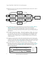
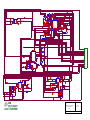
Figure 1. U603 Block Schematic
3
Motorola Proprietary Information
Topaz T2688/T200, T2988/T205 L3 Circuit Description
9. The balanced signal is then fed into U603 Pins1&2 for GSM and Pins 47 & 48 DCS.
Within the U603 the received signal will now be mixed with the RX VCO to produce
the 1st IF Frequency of 225.067Mhz. This signal is out put from U603 as a balanced
1st IF output on Pins 42 & 43 (At approximately +25dB from input signal). These are
output on the signal lines MOX and MO.
10. The RX VCO frequency is generated by the RX Dual Band Oscillator U401, which is
controlled by the Frequency Synthesiser IC, IC401 (see page ??), this is fed into U603
on Pin 39 (LO1)
11. Once the 1 st IF frequency has been fed out, it is fed through Channel select SAW
filter U604 on Pins 1&2, and fed back out on Pins 7&8 the IF then re-enters U603 on
Pin 29(IFINB) and Pin 30 (IFIN). Internal to the U603, the 1st will now be downconverted to a 2nd IF.
12. The creation of the 2nd IF is achieved in the following way: A tuning voltage
IF_TUNE, is sent from the Synthesiser IC, IC401 which drives the Varactor D601, at
approximately 1.5V IF_TUNE will drive D601 to produce an output frequency of
540Mhz. This is then fed into U603 Pin 33.
13. Within the U603 the 540Mhz will be go through a ‘Divide by 2’ divider to give
270Mhz, this will be mixed with the incoming 1st IF of 225Mhz, to give a resultant
2nd IF of 45Mhz, this is then tuned by the 45Mhz tank Circuit consisting of C637 and
L616. The 45Mhz signal carrying the modulation, will then be fed into a phase
comparator, where it will be demodulated by a reference 45 MHz signal created form
the 540Mhz signal which has passed through the ‘divide by 2’ and then though a
‘divide by 6’ divider.
14. We now have our balanced demodulated RXI and RXQ signals, which are fed out on
Pins 20, 21, 22 and 23 are fed to the VEGA IC on Pins 51, 52, 53 & 54.
15. The VEGA IC is split into 3 sections:
? The Voice Processing portion of the IC includes the microphone and speaker
amplifiers, ADC and DAC, speech digital filtering and a serial port.
? The Base-band processing section includes a 2-channel uplink and Downlink
path, a serial port and a parallel port.
The uplink path performs GMSK modulation, D/A Conversion and smoothing
filters to provide the RF circuit with I & Q signals.
The Downlink path performs anti-aliasing (this is where we filter out signals that
are lower than our expected frequency, which are created through under
sampling.) A/D Conversion and channel separation filtering of the I and Q
signals. The serial port allows base-band data exchange with the DSP, with the
Parallel port controlling timing signals.
? The VEGA also performs auxiliary RF functions such as AFC (Automatic
Frequency Control) and AGC (Automatic Gain Control)
4
Motorola Proprietary Information
Topaz T2688/T200, T2988/T205 L3 Circuit Description
16. Within the VEGA IC the path of the base-band RXI & Q data from the TX / RX IC
takes the following route.
Calibration
Offset
RXI
RXQ
Anti-Aliasing
Filter
Sigma / Delta
ADC @ 6.5MHz
Digital
Filters: ? 24
Anti-Aliasing
Filter
Sigma / Delta
ADC @ 6.5MHz
Digital
Filters: ? 24
To Baseband Serial
Interface
Calibration
Offset
17. The RXI and Q signals from the RX/TX IC enter the VEGA IC (BDLIP / BDLIN /
BDLQP / BDLQN) and follow identical paths. The first stage is through a
continuous-time second order anti-aliasing filter, which serves 2 functions: 1) to
interface between RF logic and on-chip circuitry and 2) to prevent aliasing during the
ADC process.
18. The signal is then fed into a Sigma – Delta ADC sampling at 6.5MHz, and is fed out
as a 3-bit word. This is then fed into a set of digital filters, that will decimate (break
the signal into piece parts) to give us an overall sampling rate of 270.8KHz (? 24).
This gives us a low enough frequency for adjacent channel rejection and therefore
channel separation.
19. Calibration of the IQ paths is achieved by internally shorting out the 2 input I paths,
and then the same again on the 2 input Q paths the digital value measured will then be
stored in a register. Once the RXI and Q paths are reconnected to the circuitry, again
the calibration process takes place and the offset value is calculated.
20. From the VEGA IC, the information is looped through to the GEMINI IC on the
Base-band serial interface, consisting of BDX, (Base-band Data Transmit) BCLKX
(Base-band Transmit Clock) and BFSX (Base-band Transmit Frame synch). See
below for timing diagram:
BCLKX
BFSX
A15
5
A1
A0
Motorola Proprietary Information
BDX
Topaz T2688/T200, T2988/T205 L3 Circuit Description
21. Within Gemini general GSM processing takes place, such as:
? De-Interleaving : Interleaving is a way in which the information that is to be
transmitted is jumbled around before it is sent i.e.
If we wish to send the information ‘They must read this’
T H
M U
R E
T H
?
E
S
A
I
Y
T
D
S
And we lose the information during the time
that ‘must’ is being sent. Then we will lose a
whole word.
However if we jumble the bits around that make up the words, i.e. transmit in a
different order.
T
M
R
T
H
U
E
H
E
S
A
I
Y
T
D
S
If now during the same time frame we lose the same
amount of information, and then we will only lose a small
part of each word
?
Channel De-Multiplexing – this is where we decode the signal that was transmitted,
encryption at the transmitter ends is usually done by X-ORing the information.
?
Forward Error Correction Decoding – This is where the redundant bits of data that
were added in the transmitter are removed, and the information that is received can be
processed. The redundant bits are added in various quantities dependent upon the
signal quality. This means if some data is lost whilst travelling OTA then, for
example, instead of 8 bits of speech data being lost, only 4 bits of speech and 4 bits of
redundant data.
?
De-Segmentation and CRC Attachment analysis. – During the transmission
process the data is broken into packets of various lengths (No of bits). These packets
are then processed to give a checksum of what should be expected at the receiver.
Once in the GEMINI the information received is processed, and the two checksums
compared. From the analysis, the correct algorithm for repairing any data corruption
can be implemented.
22. The processed digital audio from the Gemini is then returned to the VEGA IC on the
Voice-band serial interface VDX (GEMINI Pin 85 to VEGA Pin 14) clock,
VCLKRX and Frame synchronisation signal, VFSRX.
6
Motorola Proprietary Information
Topaz T2688/T200, T2988/T205 L3 Circuit Description
23. The processed digital audio is received from the Gemini at 8Khz, from here the signal
is interpolated within a speech-digital infinite duration impulse response filter (IIR)
(i.e. that is, for the data coming in, the adjacent bits of the data being looked at are all
synchronised and an average taken. From this a prediction of events can be
calculated) also the sampling rate is increased to 1Mhz and the speech bandwidth is
limited by high and Low pass responses.
24. The signal is then fed into a Sigma-Delta Modulator for D/A conversion this will
then give a 1 bit over-sampled signal
25. This over-sampled signal (we over-sample to allow much cheaper and easier
reconstruction of the received signal) is now D/A’d and a high frequency noise tone is
injected into the signal. This noise will be used for programming the PGA. There are
7 programmable gains and 1 mute function.
26. The noise is then removed in a smoothing filter and the appropriate gains or
attenuations made.
27. The converted speech can then take 1 of 2 paths.
28. Path 1 to the Internal speaker LS1, the audio is fed out of the VEGA on Pins 32 &
33, and fed directly to the speaker, voltage suppressers U4 and U5 are responsible for
ESD protection. The speaker is situated in the front housing of the unit and is
connected to the main PCB through 2 contact springs.
29. Path 2 to an External Speaker, the audio is fed out from the VEGA IC on Pin 34
AUXO, it passes through Connector 3, J10 which is a jumper connector for JTAG
purposes. From here it is fed to Pin 4 of the External Connector J40.
From Serial
Interface
IIR
Filter
Interpolation
filter
Sigma – Delta
Modulator
1 Bit
DAC
Side-tone
AUX0
Auxiliary
Amp
EARP
Ear-piece
Amp
EARN
7
Motorola Proprietary Information
Smoothing
Filter & PGA
Topaz T2688/T200, T2988/T205 L3 Circuit Description
TRANSMIT
30. There are 2 sources of input audio:
31. Auxiliary Microphone is fed in through J40 External Connector Pin1 and is fed
through Jumper Connector J8 (JTAG Use), and is amplified through the BQ5 circuit,
supported by the voltage DVCC. The input signal is fed onto the base of Audio
AmpBQ5, amplified, and fed out of the collector as AUXI.
32. The Internal Microphone X1, uses the circuit R14 / R15 / C22 / C23 / R17 / R18 to
provide microphone biasing, the biasing support voltage being fed from the VEGA IC
from Pin 26. (Gain approximately 27dBm)Voltage suppressers U48 and U49 provide
ESD protection to the circuit.
33. If both inputs are active then, output signal from the internal microphone will be used.
34. The input analogue audio is then routed to the VEGA IC Pins 28 & 29. Within the
VEGA the analogue signal will be driven through a PGA with a gain of between –
12dB to +12dB in 1dB steps.
35. A Sigma-Delta Modulator converts the signal from analogue to Digital, sampled at
1Mhz. The signal is the decimated and the sampling rate taken down to signal
samples at 8Khz.
MICBIAS
MICIN
Bias
Generator
MICIP
Microphone
Amp
AUXI
Auxiliary
Amp
PGA
Sigma -Delta
Modulator
Decimation
Band-pass
Filters
To Voice
Serial
Interface
36. Once again, as in RECEIVE, the loop between the VEGA IC and the GEMINI IC is
put in place for standard data processing.
37. The transmitted signal is sent to the Gemini IC over the Voice-band VDR Line
VEGA Pin 14 and is clocked by VCLKRX Pin 16. The signals are then received by
the Gemini IC on Pins 97 & 98 respectively. Synchronisation is achieved using the
frame synch signal VFSRX (VEGA Pin 13 / GEMINI Pin 96.
38. After processing, the Base-band signal information is transferred back to the VEGA
IC using the base-band lines, BFSR / BDR / BCLKR / (VEGA Pins 6, 4 & 5 and
GEMINI Pins 74 / 75 / 76 respectively)
39. Within the VEGA IC, the received information will now be modulated by GMSK.
8
Motorola Proprietary Information
Topaz T2688/T200, T2988/T205 L3 Circuit Description
40. The processed information is sent along the Serial Base-band interface, and is fed into
a register before being differentially encoded. The encoded signal is then applied to a
Sin / Cosine look up ROM where the GMSK TX I & Q ‘words’ are generated
(interpolation ratio of 16)
41. The I & Q words are the sampled at 4.33Mhz (16 X 270Khz) and applied to a high
speed 8 bit digital to Analogue converter, any image frequencies created during this
process will be removed by a subsequent Bessel Filter.
42. The burst length will be determined by the pulse width of BENA Pin 71 (when
BULON is active Pin 74, actual effective transmission burst length = BENA +32 ¼
bits)
43. Calibration of TXI & Q paths can be set during the BCAL timing window.
44. The analogue information, is now sent from VEGA Pins 57 – 60, to the TX / RX IC
on the TX I & Q lines Pins 13 – 16
BS
/
135MHz, (DCS)
540MHz, (GSM)
TXI
TXQ
45. The signal routing for the TX I & Q through the TX / RX IC is as follows:
46. The TXI & Q signals are routed to 2 modulators. At the same time, from the
Varactor D601, the 540Mhz signal, as produced in RECEIVE, is injected into the TX
/ RX IC on Pin 33, the signal is then amplified and divided by 2 (for GSM).
47. The 270MHz is then fed into a band select switch, and onto a phase splitter / shifter
which contains a 90o offset circuit. The resultant signal is then fed into the 2
modulators to be modulated by the TXI & Q data.
9
Motorola Proprietary Information
Topaz T2688/T200, T2988/T205 L3 Circuit Description
48. These 2 paths are then summed to give a single IF modulated signal, which is then
amplified.
49. From here the output current used to drive the TXVCO will be generated. The
feedback from the TXVCO (DCS or GSM) is mixed with the RXVCO frequency to
produce a reference frequency of 270Mhz. This is then mixed with the modulated IF
with the phase comparator giving an output proportional to the difference between the
phase vales of the 2 frequencies.
50. This output current is fed out on TX / RX IC Pin 11 (PLLOUT). R614 is used to
control the current out from PLLOUT.
51. The VCO driving current is then passed through the loop filter made up of R626 and
R627, C645 and C647. (C647 is a polyester capacitor used to ensure low noise). The
purpose of the loop filter is to prevent any overshoots due to channel changes, being
transmitted to the TXVCO. The TXVCO driving voltage is between 0.8V – 2.0V.
52. The drive current is fed into the TXVCO U606 on Pin 6, with the TX frequency
being fed out on Pin 1. The voltage TX2V8, which is switched by the signal
TXVCO_OFF, supports the TXVCO. The signal BS Pin 5 controls whether the
TXVCO produces a DCS or GSM output.
53. As the TXVCO produces both GSM900 or DCS1800 frequencies from the same
output line, the signal must be fed into a diplexer U605, this circuit uses inductive
properties to effectively delay 1 frequency compared to the other and therefore split
the paths, between the GSM and DCS frequencies.
54. The output frequency then takes 2 paths:
55. Path 1: The output signal is attenuated through R615-R622, coupled through C631
and C632 and fed into the TX /RX IC on Pin 8 (DCS) and Pin 9 (GSM). This will
then be used as the feedback for the TXVCO Phase lock loop as discussed in point
49.
56. Path 2: The signal is output as TX_GSM or TX_DCS to the PA.
57. The PA U201 is a Dual package three stage PA that is split into the GSM and DCS
part. The supply for the PA is VBAT 3.6V(depends on battery charge level) on Pin 6
(front stage) and Pin 8 (back stage).
58. Band selection is done with BS (Band Select). DCS high and GSM low level.
Signal inputs on pin 2 and 4 from the TXVCO diplexer U605 are TXDCS and
TXGSM. Amplified outputs are Pins 10 and 12.
10
Motorola Proprietary Information
Topaz T2688/T200, T2988/T205 L3 Circuit Description
59. Power Control is achieved in the following way:
60. RAMP is connected to the Gain Control circuit U202 Pin 3. This is the positive input
of the comparator. This is the same ideology as the AOC line in Whitecap products.
VBAT is connected to the negative comparator input on Pin 4 to compare changes on
the battery level that causes lower or higher gain of the PA
Output of the Comparator U202 is the signal APC (Automatic Power Control) Pin 1
that drives the gain input of the PA U201 Pin 14. This is fed through Q202, which is
implemented as a safety latch. In TX Mode, the right side of Q202 is biased on from
VBAT on Pin 4; this allows the APC voltage to vary the PA Drive.
In TX Background mode or RX mode, PA_ON is low, this shorts the left side of
R298 (VBAT) is shorted to Earth.
APC is also controlled in unison with the handset temperature. Thermister TR1
(which is supported by the voltage AVCC ) gives a voltage reading, which is
proportional to the current handset temperature. This is fed back to VEGA Pin 40. As
the temperature goes up the APC line is backed down slightly.
61. Sensing the high current flow to the PA back stage, Pin 8, controls the PA power
saturation. The Sense Resistor, R203 (0.033 ohm) is used to sense the voltage
variations on the VBAT line when the PA draws more or less current and is
connected to Pin 4 of Q201. The transistor is biased on using VBAT (Pin 5) and the
change in voltage over the sense resistor is throughput from Pin 4 to Pin 3. From here
it will vary the non-inverting input of U202 therefore changing the APC level.
62. Expected DC level at Pin 3 Q201 is 3.4V for PA off, 3.3V for Power step 15 and
3.2V for power step 5.
63. The second part of Q201 Pin 1 to 3 is used to inverse the TXON on signal as
TXVCO_OFF to switch Q603.
If TXVCO_OFF is low the TX VCO is on.
64. From the PA, the RF is fed out to the RF Switch U501 on Pins 1 (GSM) GSMPA, or
Pin 11 DCSPA. The operation of the RF Switch is explained in Point 4.
65. The appropriate RF signal will then be fed out to either the Antenna ANT 1 or to the
Auxiliary RF connector U113.
Synthesiser IC IC401
66. The synthesiser IC is responsible for outputting control signals to both the RX and
TX VCO’s. The IC is divided into an IF section Pins 2 - 7 and an RF Sectio n Pins 8 –
12.
67. Before any outputs from the IC can be used a reference must be made available. For
this we use the system clock. This clock is a 13Mhz clock which is generated in the
13Mhz crystal oscillator, the tuning voltage is generated as the signal AFC from the
11
Motorola Proprietary Information
Topaz T2688/T200, T2988/T205 L3 Circuit Description
VEGA IC and has a range of approximately 1.2V – 1.5V. The Oscillator supply is
generated from the Base-band Voltage Regulator U27 Pin 24 (VTCXO 2.8V). The
13Mhz is buffered by IC402 before being O/P as 13MHz to VEGA for use as the
system clock.
68. At the same time it is input to the Synthesiser IC on Pin 1 OSCin, from here the IF
tuning voltage IF_TUNE as spoken about in points 12 (RECEIVE) and 46
(TRANSMIT) to drive the 540 / 135MHz Varactor diode.
69. All the controlling signals for the IC are generated from Gemini and enter on Pin 14
DATA, the signals are clocked in (Pin 15 CLK) and the IC is enabled using the
control logic SYNPRG on Pin 13(LE)
70. The IF Support voltage for the IC is SYN2V8, a 2.8V support, generated in the RF
Voltage Regulator IC301 Pin 2 (OUTC). A sample of this voltage is taken to ensure
the synthesiser IC is switched off during idle time. This sample is fed into Pins 6 and
7.
71. The Feedback from the 540 / 135MHz Varactor diode is returned to the IC as the
signal LO2 and is fed in on Pin 3 (finif). To complete the phase lock loop.
72. On the RF side, the supporting voltage is again SYN2V8 and enters on Pin 11
(vccrf). The charge pump output for the TXVCO is fed out on Pin 8 (Dorf) to the
RXVCO U401 Pin 3. U401 is supported by SYN2V8.
73. The band select signal BS enters U401 on Pin 4 and will select the appropriate output
to either GSM or DCS on Pin 1. The output will then be fed out to the TX / RX IC as
LO1 to create the 1st IF, and also a sample will be fed back into the Synthesiser IC to
provide Phase Lock Loop feedback.
Power up Sequence
74. The main core of the power up sequence next to the operating software is the Power
Management IC U27. U27 contains 4 Voltage regulators.
? DVCC – 2.765V @ 100mA and provides the Base-band logic supplies. Pin 2
? AVCC – 2.765V @ 130mA and provides for analogue voltage supplies. Pin
27
? VTCXO – 2.765V @ 5mA – for use to drive the system 13Mhz clock. Pin 24
? VRTC – To charge to the Real Time Clock battery U32 (when battery voltage
falls below 1.2V). Pin 8
75. The battery voltage VBAT on Pin 1 supplies U27.
76. Once power is supplied to the unit, there are a number of ways that the unit can be
powered up. The input pulse is a 40mS +ve going pulse through U53 and U54 and
onto U27 inputs Pins 4&5,
12
Motorola Proprietary Information
Topaz T2688/T200, T2988/T205 L3 Circuit Description
These are:
? Power on generated by set alarm, which is generated from the RTC (the alarm
is set into the menu structure of the phone). U54 Pin 2
? IO2, software originated power on from Gemini Pin 112. U54 Pin 1
? From depressing the Power On key giving the signal PWR. U53 Pin 2
? From the External Charger (CHGERP). U53 Pin 1
77. As the unit begins to power up the reset signal is generated, again a +ve going signal.
Charging C57 generates the charge for the reset signal.
78. As for the GCAP the Power Control IC also interfaces with the SIM Card, VCC for
the SIM card is provided by Pin 20, onto SIM Block Pins 4 & 5. However the
occasional need for 5V SIM is provided using the input from the scaled DVCC on
Pin 17 and the charge pump C53 Pins 21 & 9.
79. Data is read from the SIM card on pin 2 of the SIM block I/O into U27 Pin 15 (IO)
and transmitted to the Gemini from U27 Pin 11 (S-IO). Also from Gemini are the
SIM CLK U27 Pin 13[in] & Pin 19 [out] (SIM Block Pin 1) and the SIM Reset U27
Pin 12 [in] and Pin 16 [out] (SIM Block Pin 3)
80. SIM I/O also ac ts as a SIM Presence detect signal.
81. Power for the unit can be taken from either internal Battery or from an external
source. The battery has 4 contacts, from battery connector JP2
? Pin 1 Supplies VBAT directly
? Pin 2 BATEMP is used to monitor Battery temperature during charging, and is
fed to VEGA for A / D processing.
? Pin 3 BAID is Battery ID and is used for the detection of different types of
batteries.
? Pin4 is ground
Alternatively the VBAT source can be taken from an external power source, this
originates at the I/O connector U40 Pin A3, with U36 providing ESD protection, the
signal is then fed as CHGERP, and through Fuse F1. As mentioned in Point 76 this
will ensure the unit powers up but will also pass through BQ3 and protection diode
D14 to provide VBAT. D15 limits input voltage to <6V
82. U30 is used to detect the charger and is supported by DVCC, once detected an
interrupt is sent to Gemini as IO9
83. For the Initial charge at low battery voltage, as before the input voltage at CHGERP
is approximately 6V,CHGERP originates at U40 Pin T3 with T1 as its respective
Ground
84. NOTE: If a desktop charger then I06 is used to communicate to the Gemini the status
of the charging indicator on the charger.
13
Motorola Proprietary Information
Topaz T2688/T200, T2988/T205 L3 Circuit Description
85. This will began to charge the battery through BQ3. (BQ3 fully open) The voltage
divider R111 and R112 puts a voltage of 4V onto the source of BQ6. During this time
C81 will be charged (approximate charging time is 3 – 5 Seconds.
86. When the charge in C81 reaches 4V the, the S-G bias on BQ6 will be 0V, which will
effect ively turn off BQ6, this in turn has the effect to switch Charging Control IC U29
off which will turn off BQ3.
87. For Normal charge the phased charging values stored in the EEprom will be D/A’d
then sent as signal IO11 which will control the gate of Charging Control IC U29
which will vary the gate of BQ3. This allows us to vary the charge onto the battery.
88. An exception to the above exists if a car kit is being used in which case, Ext. Power
will be input into the phone on the I/O connector Pin 11, with U19 provide ESD
protection as the signal IOPN11.
89. It will then be fed through Fuse F2, and onto the source (S1) of Dual FET U26, the
amount of current that is passed through to VBAT is controlled via software IO1 by
U25
90. For Power output when using the data cable, VBAT is fed onto the source (S2) of
U26, with U29 providing gate bias. D12 is forward biased for this 1 application.
91. The real time clock is generated by crystal X2 and runs at 32.768MHz. It is driven by
the charge pump from U46 Pin 1 (OSC1).
Synchronisation is achieved by IO14, which is clock generated by Gemini pin 50,
with the IC enabled by Chip Enable RTCCE Gemini Pin 117.
The re-chargeable RTC battery U32 provides power for U46. As mentioned in Point
74.
Pin3 nINT provides the alarm interrupt to power the unit on at a specified time.
92. U47 is the 1.8V regulator used to Power Gemini, supported by VBAT and is powered
on at the same time as the Power Control IC U27 (Pin 1 CTRL) and is supported by
VBAT. The 1.8V regulated voltage is fed out to the Gemini as PVCC18.
Memory
93. Flash U23 is split into Operating Software memory 12Mbit and EEprom Memory
4Mbit. Supported by DVCC on Pin G4. Chip enable NROMCS (N signifies active
low) from Gemini Pin 17 onto Flash Pin F1. Boot-code is contained within the IC
NFOE, Pin G1 (Active Low Flash Output Enable) is used to instruct Flash that
Gemini want to read or write form the device. DLPWR is not used.
94. SRAM U22 is a 2Mbit device, supported by DVCC on Pin E1. SRAM is Chip
enabled by NRAMCS Pin G3.
14
Motorola Proprietary Information
Topaz T2688/T200, T2988/T205 L3 Circuit Description
Display
95. The LCD module is a 98 X 64, Chip on Glass device and measures 37 x 33mm with a
polyamide foil connection to the PCB through U24. Support for the LCD is through
DVCC.
96. Contrast control is achieved by the variation in voltages, which are stored in C40
through C44 and DC / DC LCD driving voltages provided by C45 through C48.
97. Data to and from the LCD is though the data bus D0 – D7, U24 Pins 16 – 24
98. Chip select is sent from Gemini Pin 48 to LCD Connector Pin 28, with the Reset on
connector on Pin 27.
Vibrator and Alert
99. The vibrator is driven by the signal AAGC which originates from VEGA Pin 45, this
signal is applied to the base of Dual NPN / PnP transistor U44, this then causes the
second transistor to conduct forcing the collector high. This then effectively give s the
vibrator support voltage VBAT a path to earth through BQ1
100.
U6 provide EMF protection.
101. The buzzer / alert is operated, using the signal BUZZER from Gemini Pin 20,
this signal forces BQ4 to conduct creating the current path for the buzzer U8 support
voltage VBAT to earth.
102.
U7 Provides EMF protection for the buzzer.
Keypad and Back lights
103. The backlights are split into 3 for the LCD (D1 – D3) and the keypad backlights
of which there are 8 (D4 – D11). The backlights are switched on using the signal
LEDON (This is generated from Keypad detect switch U34 and is switched by the
signal B L from Gemini Pin 134. LEDON then forces BQ2 to conduct allowing the
support voltage VBAT to illuminate the backlights.
104. The keypad is made up of a 4 column x 5 Row matrix, with the signals ROW4 –
ROW 0 being generated from Gemini Pins 126 to Pins 122 respectively. The column
signals, COL3 Gemini Pin 129, COL2 Pin 128, COL1 Pin 133 & COL0 Pin 132.
105. The 2 signals ROW4 and COL4 are used as outputs from the Gemini to Keypad
detect switch U34 to inform the unit to switch on during sleep mode.
15
Motorola Proprietary Information
Topaz T2688/T200, T2988/T205 L3 Circuit Description
106.
The keypad matrix is as follows:
Function
Key
2
*
7
4
1
6
3
0
8
5
LEFT
RIGHT
#
9
YES
NO / CLR /
PWR
CLEAR
S1
S2
S3
S4
S5
S6
S7
S8
S9
S10
S11
S12
S13
S14
S15
S16
16
S17
COL0
COL1
COL2
COL3
0
0
0
0
0
0
0
0
0
0
ROW
0
ROW
1
ROW
2
ROW
3
ROW
4
0
0
0
0
0
0
0
0
0
0
0
0
0
0
0
0
0
0
0
0
No Matrix used S16 switches VBAT directly onto the PWR signal to power up
the unit.
0
0
Motorola Proprietary Information
Unique Differences Between Acer T2688 and Acer T2988
LCD holder - 42.G0119.001
Key Pad - 42.G0118.001
Volume Key - 60.G0123.001
Front/Housing listed below
60.G0122.011 (Dark Blue or Electric Blue)
60.G0122.021 (Light Green or Misty Green)
60.G0122.031 (Light Blue or Teal ice)
60.G0122.041 (Copper Orange)
There is no other hardware difference to the product. PCB is the same and other
mechanical parts are the same.
Software is different – Version 3.X is Refresh software with additional features for T2988
(Asia) and T200 (EMEA)
Additional features covered are
1. WAP
2. Quick Access Interface
3. QuickNotes (Pre-stored/User Definable SMS Message).
4. Scheduled Power On/Off
5. Thai and Vietnamese prompt
6. SIM Lock ( Network Lock)
Software version 1.X or 2.X is used on T2688 does not have the above function
CONTROL SWITCH U502
VC3
VC1
11
8
IC501
VC2
VC4
7
6
10 8
14
3
24
b
U501
CONTROL
FUNCTION
48
14 13 15
TX VCO MID CHANNELS
1
SYNTHESISER
IC
IC401
GSM: CH 62 -- 902.4MHz
DCS: CH 700 -- 1747.8Mhz
SYN2V8
from IC901
3
7
LO2 From U603
IF_TUNE
To U603
RX VCO FRQ. RANGE
GSM:1335 - 1359Mhz
DCS: 1580 - 1655MHz
R208
VBAT
2
TXVCO_OFF
VBAT
R203
Dual Band Topaz
DCS: 1710-1785MHz
PCS:1850-1910MHz
8
DCSPA
10
12
5
From VSYNEN (Gemini)
RF_ON
5
TX_GSM
TX_DCS
U605
5
3 Diplexer
16
BS
Q202
PA_ON VBAT
1
2
6
29
30
10
4
540MHz@GSM
135Mhz@DCS
36
LO2 To Synthesiser
RXI
To VEGA
PGA
90 deg
45 MHz
22
AGCPRG
DATA
CLK
28
27
26
Serial
Interface
RXQ
To VEGA
23
BS
GSM
1
AGCPRG
From Gemini
TX2V8
o
90
DCS
GSM
2
DCS
270MHz@GSM
135Mhz@DCS
TX_GSM
8
TX LOOP
FILTER
1
15
16
14
TXQ From VEGA
9
8
SEE PAGE 8 / 9 OF LEVEL 3
CIRCUIT DESCRIPTION
11
- +
U202
PA CONTROL 5
SYN2V8
IF_TUNE From Synthesiser
33
TX_DCS
IC901
TX2V8
BS
21
25
3, 4
2
RXON2
35
20
RF POWER SUPPLY
1
45
270 MHz
45MHz
24
LC TANK
R298
7
RXON1 From GEMINI
45 MHz
From VEGA TXI
U606
TX VCO
6
6
13
BS
5
1
4
3
SYN2V8
1
2
3
4
BS
4
4
U201
PA
U401 2
RX VCO
5
6
14
VBAT
1
R209
TX FRQ. RANGE
GSMPA
Q201
6
0.033Ohm
3
This line is Internal to the TX/RX IC
1
44
1
42
43
U604
8
TXON
TX_ON
D601
225 MHz
RX VCO MID CHANNELS
GSM: CH 62 -- 1172.4MHz
DCS: CH 700 -- 1612.8MHz
4
11
46
39
GSM - 124 Channels
25MHz B/W
200Khz Spacing
13MHz
to Gemmini
&
Vega
CLOCK
TX VCO FRQ. RANGE
GSM: 890-915Mhz
DCS: 1710-1785MHz
1
2
IC402
SYNPRG
From Gemini
DATA
GSMPA
1
1 3 4
U402
SYNPRG
DCSPA
11
TX / RX Switch
DCS_RX
LO1
1,2-1,5V
AFC
From VEGA
6 & 12
47
b Q602
c
e
VTCXO From U27
Power Management IC
1805-1880MHz
9
2
U601
U602
DCS_RX
7
Q601 c
e
Control
Logic
1
GSM_RX
See Circuit description Page 2 for Logic
Control truth table.
TX / RX IC
U603
HD155121F
RFIN1
4
RFIN2
5
RF_OUT 3
BS
VBAT
935-960MHz
GSM_RX
5
DIPLEXER
U113
PA_ON
This line is Internal to the TX/RX IC
CALIBRATION
RF PORT
ANT 1
RX MID CHANNELS
GSM: CH 62 -- 947,4 MHz
DCS: CH 700 -- 1842,8MHz
3
17 41 32
6 16
RAMP
From VEGA (RAMPDA)
RF2V8
RF2V8
GSM SERVICE SUPPORT GROUP
01.01.11
LEVEL 3 RF Block Diagram
Rev. 1.3
Dual Band Topaz
Michael Hansen, Ray Collins, Ralf Lorenzen-Scheil
Page 1 of 2
RX SIGNAL PATH
REFERENCE CLOCK
TX SIGNAL PATH
Orderable Part
MAIN VCO SIGNAL PATH
Non - Orderable Part
TUNING VOLTAGES
104
102
S_PWST
S_CLK
S-3V5V
(LEAD)
106
95
73
To Charger CCt IO11
BUZZER
ALRT
U8
DSP CORE
105
IO6
From Charger CCt IO9
BQ4
RIF
SIM
Interface
120
ARM
Peripheral
Interface
U40
20 PIN I / O CONN.
2
3
9
A2
10
5, 6
7, 8
DATAID Identifies DATA service
To Gemini
IO6
(DTR) To Gemini
RS232 Signalling
CHGERP
To Charger Circuit
11
IOPN11
13
ACCIN
BFSR
From GEMINI BCLKR
12
BDR
BFSX
TO GEMINI BCLKX
BDX
ACCID
VFSRX
From GEMINI VCLKRX
VDX
14
VFSRX
To GEMINI VCLKRX
VDR
GND
6
4
DSP
5
1 Serial
2
3 Interface
12
MCU
Serial
Interface
13
Voiceband
16
14
Interface
58
57
Timing Module
70
51
52
Baseband Downlink
SEE PAGE 4 OF THE
LEVEL 3 CIRCUIT DESCRIPTION
53
54
U3
APC
47
AFC
CLK
VSIM
8
Voltage Reg
RNW
B1
B3
AGC
28
27
29
NC
J8
1
4
AUXI 3
Voice Uplink
SEE PAGE 7 OF THE
LEVEL 3 CIRCUIT DESCRIPTION
RTC
2
45
AUX0
DVCC
Voice Downlink
SEE PAGE 6 OF THE
LEVEL 3 CIRCUIT DESCRIPTION
34
45
DVCC
LS1
SPKR
J10
2 1
e
LCDRST
NFOE
RTC BATT
U32
VBAT
8
RNW
U46
X2
TXI
TXI
To U603
TXQ
TXQ
2
Control Logic
PWR U53
U54
2
3 3 2
1
U35
3
5
3
1
13MHz
To Gemini
PVCC18
4
RXI
RXI
From U603
RXQ
RXQ
IO14
RTCCE
1
1 U47
AVCC
IO2
From Gemini
6
VBAT
D14
for detection
To Gemini
IO9
RAMPDA To U202 (RAMP)
S
BQ3
D
RX SIGNAL PATH
G
D16
TR1
BATEMP From
Batt
BATID
U30
F1
CHGERP
From I / O Connector
BQ6
C81
BATEMP
BATID
TX SIGNAL PATH
BATTERY
JP2
1
2
3
4
MAIN VCO SIGNAL PATH
TUNING VOLTAGES
REFERENCE CLOCK
Orderable Part
IO11
From Gemini
ACCID
F2
D
S
D2 U26
IOPN11
From I / O Connector
Pin 11 U40
D12
U29
Non - Orderable Part
Data Cable
G
b
VIBRATOR
COL0
AVCC
39
A0
ROW1
COL1
NROMCS
U26
c
ROW2
DVCC
U44
BQ1
5&4
DVCC
Supply
&
Ground
32 33
ROW0
COL2
COL3
AFC To 13Mhz Clock Cct
37
Auxiliary 38
ADC
U28
3 SIM
4 5
A1
X1
MIC
NCSO
2
1
ROW3
ROW4
25
I/O
1
40
DAI
Interface
1, 24
28
25
26
27
SIM_PD& SIM I/O
20
NRESET
SEE PAGE 8 OF THE
LEVEL 3 CIRCUIT DESCRIPTION
Bus
Controller
SIM
Interface
15
19
16
Voltage Reg
2.765V@5mA
24
VRTC
NRAMCS
E2
4 Mbit B4A4
60
59
LCDRST
DVCC
F1
Baseband Uplink
NRESET
RST
VTCXO
13MHz
U23 F6,G4,
FLASH
12Mbit G1
Serial
13
16
15
Voltage Reg
2.765V@100mA
Voltage Reg
27
2.765V@130mA
AVCC
Analog
B3
VEGA
DVCC
RNW
To VEGA
Dual Band Topaz
B2
2
RS232 Signalling
U22
SRAM A3
2 Mbit
G2, G3
DATA BUS
VBAT
U27
PVCC18
A0 To Display
ADDRESS BUS
9, 10
11, 12
13, 14
15
POWER MANAGEMENT IC
To Display
VEGA / GEMINI
COMMUNICATION
BUS
NRESET
S16
Keypad
Backlights
To Gemini
DVCC
Baseband
DATA BUS
BQ2
DATA Bus
PWR
ADDRESS BUS
110 - 114 & 105
LEDON
From Gemini
A3
Not Used
JTAG Only
Memory
Interface
U34
2, 4
5, 6
7, 8
KEYPAD MATRIX
13
U
Wire
LCD
Backlights
From Gemini
COL4
13MHz
TX_ON
RXON1 To U603
RXON2
IO2 To On Control
NRAMCS
NROMCS
RNW
NFOE
DTATID
NCSO
NRESET
VBAT
From Gemini
ROW4
BDX
109
TSP
50
72
1,8,30,49
57,66,87
121,140
U1
128
56
COL4
ACCIN
VFSRX
VCLKRX To / From VEGA
VDX
VDR From Vega
13MHz
BFSX
From U402
BCLKX From VEGA
112
13
16
20
21
ACT
I/O
122
. General
126
129 Purpose
130
132
133
COL0,1, 2, 3
96
98
85
97
86
101
69
Central
RISC Processing
Unit
TO RF_ON (RF PSU) VSYNEN
ROW0,1, 2, 3, 4
BCLKR
To VEGA
BDR
BFSR
18
Time
Processing 118
70
Unit
ARM 7
(APIF)
U24
76
75
74
84
50
117
To RTC IC IO14
U46
RTCCE
PA_ON
GEMINI
S_I/O
S_RST
S_CLK
S_PWST
S_3V5V
To U27
Power Management IC
SYNPRG
To Synthesiser
AGCPRG
To TX / RX IC
100
103
S_I/O
S_RST
119
LCD Drvr
VBAT
62
56
80
79
59
Contrast Cntl
(AGCPRG) AGCA
ACCIN
(CLOCK) SYNCLK
(DATA) SYNDAT
(SYNPRG) SYNENA
BS
U25
G2
S2
VBAT
GSM SERVICE SUPPORT GROUP
01.01.11
LEVEL 3 RF Block Diagram
Rev. 1.3
Dual Band Topaz
Michael Hansen, Ray Collins, Ralf Lorenzen-Scheil
Page 2 of 2
R55
TP27
AVCC
(2)
1
BGND
IO2
BGND
DAN222
VBAT
D
D14
(4)
FDG312P
(3)
C59
SCL
VSS
SDA
C75
BGND
BGND
BGND
4.7UF(10V 0805)
8
LEDON
U47
TK11218BMCL
VIN
TP21
X
X
BGND
BGND
BGND
R107
BL
DVCC
100K
U44
BGND
1
1
1
3
VBAT
TP43
1
U6
DAN222
+
M1
BCR22PN
A
LA4-424BD -
2
1
2
LEDON
1
BQ1
AAGC
BQ2
MMBT4403LT1
1
TP45
R19
1K
BGND
1
DVCC
BC818-25W
3
R24
47K
AVCC
BGND
BGND
ROW4
BATTERY CONN
2K
BGND
CLK
C61
BCR22PN
R43
GEMINI_C07
RST
100PF
2.2UF(T 10V)
PVCC18
1000P
VPP
C60
U35
IO11
C72
R121
0
CTRL
BGND
C71
3
BGND
BCLKR
BDR
BFSR
C85
4
VOUT
NBP
1
PVCC18
TP28
BGND
TSPDI
I/O
RTCCE
VBAT
C68
JP2
TP22
IO14
0.1UF
1
2
3
4
BGND
BGND
6
1
BGND
R89
47K
5
VBAT
COL4
R72
100K
6
BGND
TP20
R112
2K
R88
47K
7
X
U34
UMH10N
VBAT
BATEMP
BAID
C81
SYNCLK
SYNDAT
2
3
BGND
RB491D
R82
10K
0.1UF
270K
D16
RB520S-30
S
nINT
TP19
(1)
R78
BQ6
D
BGND
(3)
S
CLK
100K
NDS356P
R111 R106
1K
2M
NEMU1
NEMU0
4
VDD
OSCO
R91
BGND
BQ3
X
BFSX
BCLKX
BDX
3
DMX-26S
OSCI
3
R104
(5)
DAN222
R103
R77
2
47K
BGND
TMS
TCK
TRST
TDI
TDO
1
100K
TP48
4
4
2
R76
100K
R73
10K
V_RST
FDP
3
2
PWR
X2
C67
2PF
0.1UF
2
3
BGND
R75
10K
C58
U54
1
IO9
4.7K
S_IO
IO9
VCLKRX
VDR
VFSRX
VDX
SYNTHCLK
SYNTHDATA
U53
R90
1
MS614-FL28N
+
V
-
U32
FUSE(0603)
PCF8563
U46
R71
TP29
DVCC
1
1
TP23
CHGERP
R74
15K
5
5
6
4
BCR22PN
IO6
S_3V5V
S_PWCT
S_RST
S_CLK
1
1
1
R101
10K
F1
[DTR]
BGND
GND
TP4
U30
1
TP3
1
BGND
100K
AGND
BGND
2
1
R68
1
4
5.6K
TP31
R67
100K
BGND
4
TP2
GND
4.7UF(10V 0805)
C57
TP56
5
1
VCC
SIM SOCKET
0.47UF
3
TP1
U28
2
C55
S_PWCT
S_3V5V
VBAT
37
38
39
40
41
42
43
44
45
46
47
48
49
50
51
52
53
54
55
56
57
58
59
60
61
62
63
64
65
66
67
68
69
70
71
72
BGND
R63
2.2K
6
1
BGND
BGND
R100
10K
DVCC
R102
IO11
10UF(10V 1206)
BGND
BGND
BGND
C54
2
A6
A7
A8
A9
A10
A11
5
20K
DVCC
R60
100K
C66
0.01UF (X7R)
1
AGND BGND
47K
100
R64
2K
2
A0
A1
C51 A2
A3
A4
X
A5
47K
R66
20K
1
A[0..20]
1
28
27
26
25
24
23
22
21
20
19
18
17
16
15
VBAT
AGND
VCC
VCCA
PWRONKEY REFOUT
ANALOGON
RESET
PWRONIN
VTCXO
ROW_X
DGND
CHRON
RESCAP
VRTC
VCAP+
VCAPVSIM
SIM_BAT
CLK
DATAIO
SIMON
RSTIN
SIMPROG
CLKIN
RST
SIMGND
IO
ADP3403
R65
BGND
1
RNW
NFOE
TP32
108
107
106
105
104
103
102
101
100
99
98
97
96
95
94
93
92
91
90
89
88
87
86
85
84
83
82
81
80
79
78
77
76
75
74
73
R5
4.7UF(10V 0805)
1
13MHZ
RB520S-30
G
NROMCS
U1
ADD20/ECLK
VDDS2
NRSTOUT/IO6
SIM_RNW/IO7
SIM_PWCTRL/IO8
SIM_RST
SIM_CLK
BCLKX
SIM_IO
VSS
VCLKRX
VDR
VFSRX
SIM_CD/IO9
DSPINT
FDP/BION
NBSCAN
TMS
TCK
TRST
TDI
VDD
BFSX
VDX
BDX
TDO
NEMU1/FDP
NEMU0/SIMCLKLOW
TSPCLKX
TSPDO
VSS
TSPDI
BCLKR
BDR
BFSR
ARMCLK/IO11
R4
S_IO
S_RST
S_CLK
C56
BGND
3
144
143
142
141
140
139
138
137
136
135
134
133
132
131
130
129
128
127
126
125
124
123
122
121
120
119
118
117
116
115
114
113
112
111
110
109
NRAMCS
DATA8
DATA9
DATA10
DATA11
VDDARM
DATA12
VSS
DATA13
DATA14
DATA15
LT/IO10
KBC1/RNW
KBC0/IOSTRBN
VSSLMM
KBC2/XDIO0
KBC3/XDIO1
KBC4/XDIO2
VSS
KBR0/XDIO3
KBR1/XDIO4
KBR2/XDIO5
KBR3/XDIO6
KBR4/XDIO7
VDDLMM
BU/XF
TSPACT7/INT_F
TSPACT6
NLCDCS/IO0
RXE/IO1
VSSLMM
DTR/IO3
TXD
TXE/IO2
RXD
DSR/IO4
EXTINT/IO5
1
D2
D1
D0
3
1
RTCCE
IO1
IO2 [RTS]
DTR
TXD
RXD[CTS]
DSR
VSS
ADD12
ADD13
ADD14
ADD15
ADD16
VDDS
ADD17
ADD18
ADD19
DI/X_A4
NCS0/IO15
VDDLMM
NCS1/1O14
CS2
VSS
SCLK/CLKOUT
DO/X_A1
NEECS/X_A2
NPWRCS/IO13
VDD
NTSPEN0/TSPACT8
NTSPEN1/TSPACT9
VSSLMM
NTSPEN3/TSPACT11
TSPEN4/TSPACT12
TDO_BSCAN
NTSPEN2/TSPACT10
TSPACT0/IO12
VDDLMM
TSPACT2
TSPACT3
TSPACT4
TSPACT5
TSPACT1
NRESET
2
2
1
BGND
VBAT
D15
BGND
ROW4
ROW3
ROW2
ROW1
ROW0
COL4
COL0
VCE
VDDARM
DATA7
DATA6
DATA5
DATA4
DATA3
VSSARM
VDDARM
DATA2
DATA1
DATA0
VDDS
NRAMCS
NBLE
NBHE
NROMCS
GNDANG
CLKIN
VANG
RNW
NFOE/X_A3
NFWE/X_A0
VSS
ADD0
ADD1
ADD2
ADD3
ADD4
ADD5
VDD
ADD6
ADD7
ADD8
ADD9
ADD10
ADD11
BGND
VBAT
R62
2K
TXPA
TXEN
1
1
2
3
4
5
6
7
8
9
10
11
12
13
14
15
16
17
18
19
20
21
22
23
24
25
26
27
28
29
30
31
32
33
34
35
36
1
2
3
4
5
6
7
8
9
10
11
12
13
14
VBAT
U29
1
COL2
2
BGND
UMH11N
TSPACT7
TSPACT6
D15
D14
D13
1
BGND
DVCC
D7
D6
D5
D4
D3
G2
100K
5
1
D12
VCE
IO1
6
1
TP58
D11
D10
D9
D8
VCE
R3
AVCC
U52
VOL SW
R61
BGND
DATAID [DSR]
3
2
1
U51
R26
0
2
TP57
D[0..15]
U50
R2
COL4
BUZZER
TP59
ROW2
COL0
ROW3
S2
R87
U27
47K 47K
BL
U45
G1
R59
100K
AGND
BGND
0.1UF (0603)
4.7UF(10V 0805)
R58
X
BGND
R23
47K
1
S15
KSW
[YES]
DVCC
R1
100K
COL3
COL2
COL1
COL0
C53
BQ4
MMBT4401LT1
4
S14
KSW
[9]
BGND
R57
C52
1K
BGND
C50
10UF(T 6.3V)
C65
10UF(T 6.3V)
TP30
LCDRST
100K
2
ROW4
ROW3
ROW2
ROW1
ROW0
D2
1
1
S1
UMD6N
5
S13
KSW
[#]
R20
D1
U25
1
U26
FDC6306P
3
S12
KSW
[RIGHT]
S10
KSW
[5]
TP46
2
S11
KSW
[LEFT]
S9
KSW
[8]
0.1UF
0.1UF
G
S17
KSW
[CLEAR]
S8
KSW
[0]
C12
6
0.1UF
3
C11
6
S7
KSW
[3]
10UF(T 6.3V)
VBAT
0.1UF
BGND
C13
S6
KSW
[6]
C10
3
0.1UF
C49
BUZZER2
AGND
TP53 TP54 TP55
VTCXO
1
D12
RB520S-30
GND
S5
KSW
[1]
FUSE(0603)
IOPN11
BGND
2
S4
KSW
[4]
1
S3
KSW
[7]
2
S2
KSW
[*]
F2
AGND
6
0
4
C9
S1
KSW
[2]
3
5
0.1UF
2
C8
TP24
4
0.1UF
3
C7
DVCC
3
0.1UF
U7
DAN222
5
C5
0.1UF
0.1UF
2
C4
0.1UF
C2
1
C3
0.1UF
0.1UF
4
C6
C1
L1
6
U8
1
VBAT
3
PVCC18
5
DVCC
6
AVCC
100
2
PWR
KSW
1
[NO]
[CLEAR]
[PWR]
S16
1
VBAT
R25
15
BGND
C14
A19
A18
A17
47K
A16
A15
A14
A13
A12
A20
R99
ANTENNASEL
SYNTHEN0
DIN
1
RXON
AGCA
VSYNTHEN
TP33
FSW1
FlipConn
[2]
C70
X
CALIBRATERADIO
BULON
BDLON
BCAL
BENA
NCS0
BGND
BGND
NRESET
BANDSW
SYNENA
NTPEN0
0.1UF
R44
R47
51 (0805)
24 (0805)
BGND
BGND
AGND
RXON
AGCA
VSYNEN
ACCIN
CALBRA
TPACT3
TPACT2
TPACT1
TPACT0
13MHZ
TPACT0
TPACT1
TPACT3
TPACT2
NTPEN0
TSPDI
SYNDAT
SYNCLK
D1
SYNTHDATA
SYNTHCLK
1
TP39
1
TP40
1
TP41
1
TP42
D2
D3
D4
CL220 CL220 CL220
BGND
BGND
D5
D6
D7
D8
D9
D10
D11
CL190 CL190 CL190 CL190 CL190 CL190 CL190 CL190
BGND
BGND
BGND
BGND
BGND
BGND
BGND
BGND
BGND
R42
x
D11
D3
D10
D2
D9
D1
D8
D0
D[0..15]
C38
0.1UF
A[0..20]
A0
BAID
TP38
1
BATEMP
R16
C18
100K
NROMCS
B3 BEAD
0.1UF (0603) AUXO
0.1UF (0603)
AUXI
AGND
R120
0
R14
1K
0.1UF
C17
R15
AM29DL162CB70WCI
NRESET
BGND
U48
1
R13
100
100
100
100
100
100
560
R27
X
2
2
2
2
2
1
1
1
1
1
0.1UF
0.1UF
0.1UF
0.1UF
100K (1%)
DLPWR
3
2
1
AVCC DVCC
0
C21
0.1UF
C24
0.1UF
C25
C28
BGND
C33
150PF
0.1UF
C31
0.1UF
C32
0.1UF
0.1UF
R119
C29
U49
2
VCE
100K
1.5K
C35
R93
TP8
C34
C76
X
BEAD
R22
1K
1K
R97
C36
1M
0.1UF
1
33PF
C73
X
2
C88
C83
1
U4
TP11
1
1
U9
VCE
U10
VCE
U11
VCE
TP12
DE1
S14
S13
S12
S11
S10
S9
S8
S7
S6
S5
S4
S3
S2
S1
DE2
DE3
T1
T3
T2
1
U12
VCE
U14
VCE
U37
VCE
U36
VCE
IO CONNECTOR20
VCE
100K
100PF
C80
C74
100PF
BQ5
BC818-25W
J8
0
0.1UF
3
2
1
10PF
C87
100PF
10PF
R98
560K
CON3
TMS
BGND
Revisions
GSM Service Support Group
L3 Audio Logic Schematic
Topaz
Title
BGND
BGND
BGND
BGND
C78
220PF
R122
C84
R95
680
C77
100PF
BGND
1
2
TP7
BGND
U41
VCE
TP10
1
100PF
10UF (0805 6.3V)
BGND
BGND
TP9
C37
BGND
LS1
SPEAKER
B1
R21
U5 VCE
B2
BEAD
AGND
C86
12K
BGND
150PF
TP49
DVCC
R123
AUXI
0.1UF
TP5
0.1UF
A2
A3
B1
B3
B2
100
TP52
R113
0
14
13
12
11
10
9
8
7
6
5
4
3
2
1
R81
C30
0.1UF
C27
AGND
1K
R79
2
AGND
150PF
BGND
AGND
IO6
[DTR]
CHGERP
CON3
X1
MICROPHONE 1
C20
A1
J7
VCE
4.7UF(10V 0805)
R18
R17
0.1UF
C26
C16
AGND
C82
0.01UF(0603 X7R)
C64
AGND
TP6
1K
C23
0.1UF
0
C63
ACCID
LCDRST
R116
C89
X
C62
TRST
C19
NCS0
A1
3
2
1
TCK
R109 10K
NFOE
CON3
BGND
R34
R33
R32
R31
R30
R29
R28
1
AGND
98*64 GPO LCD
BGND
BGND
R12
220K (1%)
220K (1%)
C22
RNW
R11
1
TP18
BGND
U40
VCE
TP17
1
BGND
R10
220K (1%) 68K (1%)
VEGA
0
U21
2
R41
0
D7
D6
D5
D4
D3
D2
D1
D0
DATAID
DTR
TXD
RXD
[CTS]
DSR
[DSR]
[RTS]
J9
TP37
1
BGND
100
100
1
2.2UF(0805 Y5V 10V)
DVCC
1
ACCIN
ACCID
IOPN11
R37
R36
VCE
TP16
1
D15
D7
D14
D6
D13
D5
D12
D4
2.2UF(0805 Y5V 10V)
[CI]
B4 BEAD
VBAT
AGND
1
CON3
1
AVCC
R9
U20
2
DLPWR
C48
TP47
VCE
2
R40
0
E6
F6
H6
G6
E5
F5
H5
G5
E4
F4
H4
G4
G3
H3
F3
E3
G2
H2
F2
E2
G1
H1
F1
E1
AUXO
TR1
TR_10K
0.1UF (0603)
VCE
TP14
1
DVCC
A16
/BYTE
VSS
D15/A-1
D7
D14
D6
D13
D5
D12
D4
VCC
D11
D3
D10
D2
D9
D1
D8
D0
/OE
VSS
/CE
A0
C15
VCE
TP13
2
NRESET
A15
A14
A13
A12
A11
A10
A9
A8
A19
NC
/WE
/RESET
NC
WP#/ACC
RY/BY#
A18
A17
A7
A6
A5
A4
A3
A2
A1
TP36
RAMPDA
AFCDAC
AAGC
VCE
3
2
1
1
C47
U23
D6
C6
A6
B6
D5
C5
A5
B5
D4
C4
A4
B4
D3
B3
A3
A19 C3
A18 B2
A8 A2
A7 C2
A6 D2
A5 B1
A4 A1
A3 C1
A2 D1
A16
A15
A14
A13
A12
A11
A10
A9
A20
1
U19
J10
TDI
2
DVCC
1
TP35
U18
IOGND
68K (1%)
1
2.2UF(0805 Y5V 10V)
10K
2
C46
A17
TP34
C69
U17
220PF
R92
R8
1
2.2UF(0805 Y5V 10V)
BGND
BGND
NRESET
VFSRX
VDR
VDX
VCLKRX
V_RST
U16
2
1UF(0805 Z5U 16V)
C45
UM62S2048-70
0
VDD
C86
VSS
V5
V4
V3
V2
V1
CAP2+
CAP2CAP1CAP1+
CAP3VOUT
VSS2
D7
D6
D5
D4
D3
D2
D1
D0
E(RD#)
R/W(WR#)
A0
/RESET
/CS
R38
47K
CON3
IRXN
IRXP
QRXN
QRXP
1
1
2
3
4
5
6
7
8
9
10
11
12
13
14
15
16
17
18
19
20
21
22
23
24
25
26
27
28
TDO
BGND
1
U24
1UF(0603 X5R 6.3V)
C44
R117
3
2
1
2
BGND
AVCC
1
R118
1UF(0603 X5R 6.3V)
C43
IO6
[DTR]
1
A0
A1
A2
A3
DVCC
BGND
J11
ITXP
ITXN
QTXP
QTXN
1
1UF(0805 Z5U 16V)
C42
1
TP15
60
59
58
57
56
55
54
53
52
51
50
49
48
47
46
45
44
43
42
41
BULIP
BULIN
BULQP
BULQN
AVDD2
AVSS2
BDLIN
BDLIP
BDLQN
BDLQP
VMID
DVSS3
AVSS3
APC
AFC
AGC
ADCMID
AVDD3/5
DVDD3
AVDD3
2
C41
BFSX
BCLKX
BDX
BDR
BCLKR
BFSR
AVDD1
VREF
IBIAS
VGAP
AVSS1
RESET
VFS
VDX
VDR
VCLK
SSRST
SSDX
SSDR
SSCLK
1
1UF(0603 X5R 6.3V)
D2
D1
D0
1
2
3
4
5
6
7
8
9
10
11
12
13
14
15
16
17
18
19
20
BFSR
BCLKR
BDR
BDX
BCLKX
BFSX
1
DVCC
3
BGND
TP25
X
C40
1
U3
BGND
2
C39
0.1UF
A17
A16
A14
A12
A7
A6
A5
A4
TP26
D7
D6
D5
D4
D3
AVCC
R86
1
0
A10
DVCC
1
A15
G2
H2
G3
G1
F1
C1
B1
G6
D1
F6
C6
B6
A1
A2
B2
A4
E6
C3
1
R39
#OE
A10
#CE1
I/O8
I/O7
I/O6
I/O5
I/O4
GND
I/O3
I/O2
I/O1
A0
A1
A2
A3
GND
NC
DVDD4
DVSS4
PWRDN
TRST
GNDA1
MICBIAS
MICIP
MICIN
AUXI
AVDD4
AVSS4
EARP
EARN
AUXO
GNDA2
ADIN1
ADIN2
ADIN3
ADIN4
ADIN5
RNW
A11
A9
A8
A13
#WE
CE2
A15
VCC
A17
A16
A14
A12
A7
A6
A5
A4
VCC
NC
21
22
23
24
25
26
27
28
29
30
31
32
33
34
35
36
37
38
39
40
DVCC
H3
H1
A6
H5
B3
A3
G5
E1
F4
G4
H6
H4
B5
A5
C4
B4
D6
F3
1
U22
A11
A9
A8
A13
DVDD1
DVSS1
UCLK
UDR
UDX
USEL
BDLON
BULON
BCAL
BENA
MCLK
TEST1
TEST2
TEST3
DVDD2
DVSS2
TCK
TDI
TDO
TMS
A[0..20]
80
79
78
77
76
75
74
73
72
71
70
69
68
67
66
65
64
63
62
61
IO14
NRAMCS
D[0..15]
BGND
Size
D
Date:
5 Jan 01
Rev 1.0
D70V8 (All On One Page)
Document Number
Rev
0.1
56D70V8-3
Thursday, November 16, 2000
Sheet
1
Ray Collins / Michael Hansen / Ralf Lorenzen-Schiel
of
1
EFCH9418MTY6
U601
4
TXON
GSM_RX
8
8
C605
15p
C606
10p
4
ENA
GND
VREF
3
1
C616
1p
C304
6
10u
0805C
C619
1p2
5
C305
RF_ON
C623
R609
1
Q602
BFP520 4n7
5n6
R612
10k
C628
0.1u
C624
33p
C625
10p
C632
33p
C631
10p
R617
470
TX_GSM
1
TX_DCS
1
2
3
4
5
BS
OUT
2
3
4
SW
VCC
9
8
7
VT
10
9
8
7
6
36
35
34
33
32
31
30
29
28
27
26
25
IFLO
BAND
IFVCOO
IFVCOI
VCCIF
GNDIF
IFIN
IFINB
LE
SDATA
CLK
MIX2O
C621
C620 100p
7p
D601
BBY57-02W
L609 C622
2n7 100p
R611
3k3
IF_TUNE
RF2V8
C626
0.1u
MO
MOX
L613
L614
C634
150nH
0603L
C633
150nH
0603L
C637
R623
n.m.
BS
10p
R608
n.m.
100p
7
8
9
1
C635
1.8nH
100n
0603
U604
TFS225
L616
68n
0603L
C636
L615
1.8nH
3
2
1
68n
0603L
RF2V8
C638
680p
AGCPRG
DATA
CLOCK
U605
LFDP20N0020A
AGCPRG[0..2]
R625
n.m.
RX_I/Q[0..3]
IRXP
IRXN
QRXP
QRXN
R627
47R
C660
15p
R626
56R
C645
560p
0402C
QTXN
QTXP
ITXN
ITXP
TX_I/Q[0..3]
HD155121F
LO2
120n
0603
3
DCS
4
2
2
IN
1
GSM
6
U606
ENFVZ4G00
C650
33p
3
U603
0R
C610
100p
C617
4
5
6
C641
10p
1
C640
33p
TXVCO_OFF
C649
10p
10dB_PAD
4
R622
2
Q603
2 TP0101T
3
MIXINB1
MIXIN1
RFOUT
RFIN1
RFIN2
VCCPLL
GNDPLL
VCOIN2
VCOIN1
VCCCOMP
PLLOUT
ICURAD
R614
47k
R618
100
10dB_PAD
3
R621
4
TX2V8
1
2
3
4
5
6
7
8
9
10
11
12
R610
10k
C627
1p
4
2
15p
RF2V8
C615
4p7
C614
2p
470R
L611
L610
10n
MAS9128A
Q601
BFP420
12p
6
5
4
10u
0805C
ENBC
L606
8n2
10
11
12
3
VCC
C608
0.1u
R607
3p
12n
VBAT
7
C607
100p
C609
8n2
L608
48
MIXIN2
47
MIXINB2
46
POONTX
45
POONRX2
44
POONRX1
43
MIX1OUTB
42
MIX1OUT
41
VCCMIX1
40
GNDMIX1
39
RFLOIN
38
VCCDIV
37
GNDDIV
C303
OUTC
L605
10n
2
2
C613
8
LO1
SYN2V8
C612
2p2
470R
L607
10u
0805C
OUTB
0.1u
C653
2p7
4
2
SYN2V8
OUTA
3
1
C603
L604
2n7
R605
C302
IC301
10u
0805C
RF2V8
QINB
QIN
IINB
IIN
MODLB
VCCIQ
GNDIQ
QOUTB
QOUT
IOUTB
IOUT
MIX2OB
RF2V8
C301
C652
0p5
C604
1p2
MOX
MO
C601
1p
13
14
15
16
17
18
19
20
21
22
23
24
8
RXON1
5
6
7
DCS
6
GSM
5
6
7
TX2V8
4
DCS
2
GSM
8
4
3
DCS DCS 2
2
6
1
GSM GSM
U602
EFCH9418MTY6
3
2
1
RXON2
C602
2p
4
DCS_RX
RF2V8
C646
0.1u
C647
10n
0805C
C401
LO1
SYNPRG[0..2]
15p
BASEBAND
CLOCK
OSCin
15
R401
CLK
GNDrf
IC401
1
16
VSYNEN
14
DATA
R402
33R
2
GNDif
LE
finif
Finrf
4
5
VCCrf
LD/Fout
Xfinrf
56p
R409
IF_TUNE
10
AGCA
SYNCLK
SYNDAT
SYNENA
RXON
CALBRA
1
5
8
4
SYNPRG
R408
680R
U401
BANDSW
3
1n
C416
C417
1u
0603C
33p
R413
4k7
1
R415
22k
Control
4
VCC
C424
2
0.1u
C420
1n2
0402C
C428
33p
U402
AFC
GND
3
OUT
13MHz
R411
10K
C426
10p
5
R410
22R
C415
2
1k5
5
ENFVZ4E76A
VTCXO
AFCDAC
SYN2V8
C418
15p
2
BDLQN
C422
15n
1206C
TSPEN4
TSPCLK
TSPDO
NTSPEN1
TSPACT5
TSPACT4
TSPACT6
TSPACT10
13MHz
AFC
VTCXO
VTCXO
VBAT
VBAT
RAMPDA
IC402
TC7SHU04FU
4
BDLQP
BS
C427
15p
0402C
9
Dorf
Doif
PSrf
7
0402C
C414
3n3
C413
PSif
BDLIN
SYN2V8
C409
1n
C412
1206C
47n
BDLIP
180R
11
R407
1k
6
BULQN
QRXP
R406
15p
Vccif
BULQP
QTXN
QRXN
MB15F03SL
SYN2V8
BULIN
QTXP
IRXP
12
BULIP
ITXN
IRXN
C406
3
-5dB
SYNPRG
13
C405
100p
LO2
ITXP
180R
DATA
TSPACT11
TXPA
APC
TSPACT7
3
ENE3010A
R416
1M
C425
13MHz
0R
3
3
U502
14
B1
O2
A1
B2
O0
A2
B0
VCC
A0
5
RXGSM
5
4
3
RXDCS
B
A
G
L503
0603L
5n6
L502
0603L
n.m.
TXON
DCS_RX
2n2
0402L
15
VCC
Q202
C210
TXVCO_OFF
R206
39k
C208
10p
Q201
1
3
2
5
6
R299
C209
33p
10k
0402C
1
5
2
4
6
R297
PAON
39k
0402C
4
R298
BC847PN
VBAT
47k
0402C
VBAT
L505
R208
47k
6n8
0402L
R503
3p
R209
10k
R213
270k
C211
VBAT
R215
9k1 1%
15p
R216
0R
R214
100k
4
5
3
BC847PN
VBAT
R207
11.8k 1%
IC501
TC7SHU04FU
4
C215
10nF
U202
AD8031
+
2
C216
3p
0402C
C207
33p
470u/10V/0.1R
7
L504
C206
10p
2
1
5n6
LQW1608 0603L
8
6
R203
0.033R
0805
VBAT
8
PA_ON
RAMP
3
3
BS
C205
33p
0402C
9
GSMPA
ANT1
ANTENNA
GSM_RX
74LCX00MTC
10
G
L501
0603C
33p
3
2
C502
47p
9
7
6
VCC
12
10
9
DCSPA
3n9
LQW1608 0603L
L201
5
13
A3
VC3
5
11
GSMOUT
L203
12
11
R211
150k
1
12
O1
VC2
11
GSMIN
5
13
2
11
B3
ANT
GND
10
GND
VC4
GND
6
9
O3
VC1
DCSOUT
L202
n.m.
0402L
C203
12p
0402C
13
-
8
4
TXDCS
1
2
TXGSM
C204
33p
C
4
1
GSMPA
U113
CONNECTOR
GND
U501
LMC36-07A0505A
DCSIN
3
4
TXGSM
1
7
R219
27R
APC
2
TXDCS
DCSPA
BS
1
C202
10p
R217
1k8
C201
68p
14
16
U201
RM009
7
C214
15p
15
BS
R212
240k
Title
D65 RF
Revisions
GSM Service Support Group
L3 RF Schematic
Topaz
Size
E
Document Number
{Doc}
Date:
5 Jan 01
Rev 1.0
Ray Collins / Michael Hansen / Ralf Lorenzen-Schiel
Wednesday, November 01, 2000
Rev
{RevCode}
Sheet
1
of
1
Test Mode commands for Topaz T2688
1)*#300# OK
List the Software and Hard ware version
2)*#301# OK
Full Keypads functional Test
3)*#307# OK
Engineering Test Mode
4)*#402# OK
Adjust Display Intensity/ Contrast
5)*#403# OK
List the Manufacturing Informations
6)1998 0722OK
7)*#302# OK
Master Unlock code for Phone and Sim Lock
Acoustic test*
1)greeting
2)Main VlmGain
3)Input Cal
4)Output Cal
5)Side In Gain
6)Vox Gain
7)Min Mic Engy
8)More
.1 In vlm Gain
.2 Aux Vlm Gain
.3 Silence Prd
.4 Supp Prd
.5 In Volume
.6 Out Volume
.7 Icon
.8 Image
.9 Animation
8)#303# OK
Settings Saved*
9)#400# OK
ADC, Cal val*
* use with care - contains cal factors
Thomas Tan 05/08/00
Motorola Internal Use only