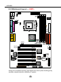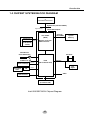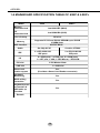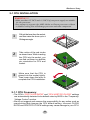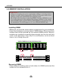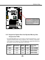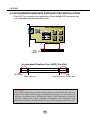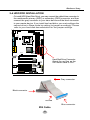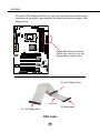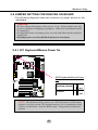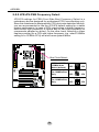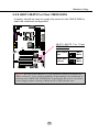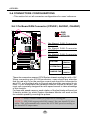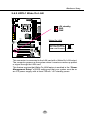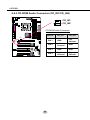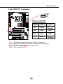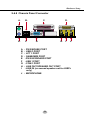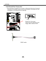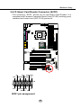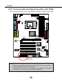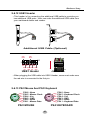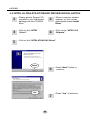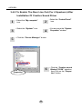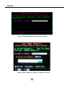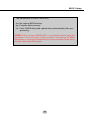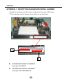
1
R
T h e
S o u l
O f
C o m p u t e r
T e c h n o l o g y
SL-65EP/65EP+
USER MANUAL v1.1
NOTICE
Product Model
Manual Revision
Release Date
: SL-65EP/EP+
: V1.1
: June 2001
T
his User’s Guide & Technical Reference is to help system manufacturers and end-users set up and install the mainboard.
Every effort has been made to ensure that the information in this
manual is accurate. Soltek Computer Inc. is not responsible for printing or clerical errors. Information in this document is subject to
change without notice and does not represent a commitment on the
part of Soltek Computer Inc.
No part of this manual may be reproduced, transmitted, translated
into any language in any form or by any means, electronic or
mechanical, including photocopying and recording, for any purpose
without the express written permission of Soltek Computer Inc.
Companies and products mentioned in this manual are for identification purpose only. Product names appearing in this manual may
or may not be registered trademarks or copyrights of their respective companies.
Soltek Computer inc. provides this manual “As is “ without warranty
of any kind, either express or implied, including but not limited to
the implied warranties or conditions of merchantability or fitness for
a particular purpose. In no event shall Soltek computer inc. be
liable for any loss or profits, loss of business, loss of use or data,
interruption of business, or for indirect, special, incidental, or
consequential damages of any kind, even if Soltek computer inc.
has been advised of the possibility of such damages arising from
any defect or error in this manual or product.
Copyright © 2001 Soltek Computer Inc. All Rights Reserved.
• Intel, Celeron, Pentium II, Pentium III are trademarks of Intel Corporation.
• Intel 82815 Graphic Memory Controller Hub(GMCH), 82801 I/O Controller Hub(ICH) are
trademark of Intel Corporation.
SOLTEK AROUND THE WORLD
SOLTEK COMPUTER INC.
Address
Telephone
Fax
E-mail
Web site
: 7F, No. 306-3, Ta-Tung Rd, Sec.1, Hsi-Chih, TaipeiHsien, Taiwan, R.O.C.
: 886-2-2642-9060
: 886-2-2642-9065
: [email protected]
: http://www.soltek.com.tw
SOUL TECHNOLOGY EUROPE B.V.
Address
Telephone
Fax
E-mail
Web site
: Hongkongstraat 55, 3047 BP Rotterdam. The Netherlands
: 31-10-2457492
: 31-10-2457493
: [email protected]
: http://www.soultech-europe.com
65EP/EP+
CONTENT
CHAPTER 1 INTRODUCTION ................................................. 9
1-1 MAINBOARD SPECIFICATION ............................................... 10
1-1.1 PROCESSOR ................................................................................. 10
1-1.2 CHIPSET ......................................................................................... 10
1-1.3 AWARD BIOS V6.0 SUPPORTING ................................................. 10
1-1.4 SOUND CONTROLLER .................................................................. 10
1-1.5 INTEGRATED SDRAM CONTROLLER .......................................... 10
1-1.6 FULL FEATURED ACCELERATED GRAPHICS PORT (AGP)
CONTROLLER .............................................................................. 10
1-1.7 POWER MANAGEMENT ................................................................ 11
1-1.8 MULTI-I/O FUNCTION .................................................................... 11
1-1.9 EXPANSION SLOTS ....................................................................... 11
1-1.10 FORM FACTOR ............................................................................ 12
1-1.11 HARDWARE MONITOR ................................................................ 12
1-2 MAINBOARD LAYOUT ............................................................ 13
1-2.1 Mainboard Layout --- 65EP ............................................................. 13
1-2.2 Mainboard Layout --- 65EP+ ........................................................... 14
1-3 CHIPSET SYSTEM BLOCK DIAGRAM ................................... 15
1-4 MAINBOARD SPECIFICATION TABLE OF 65EP & 65EP+ .... 16
CHAPTER 2 HARDWARE SETUP ......................................... 18
2-1 CPU INSTALLATION ............................................................... 19
2-1.1 CPU Frequency ............................................................................... 19
2-2 MEMORY INSTALLATION ....................................................... 20
2-2.1 Supported System Bus And System Memory Bus Frequencies Table .... 21
2-3 ACCELERATED GRAPHICS PORT(AGP) PRO INSTALLATION ... 22
2-4 HDD/FDD INSTALLATION ....................................................... 23
4
Introduction
2-5 JUMPER SETTING FOR DEVICES ON BOARD .................... 25
2-5.1 JP1 Keyboard/Morse Power On ...................................................... 25
2-5.2 JP5/JP6 Bus Clock Select ............................................................... 26
2-5.3 JP2/JP8 USB Port Select (1) .......................................................... 27
2-5.4 JP9/JP10 USB Port Select (2) ........................................................ 28
2-5.5 JP11 USB Wake Up ........................................................................ 29
2-5.6 BIOS Boot Block Lock (JP16) ......................................................... 30
2-5.7 JP21 On-Board Creative Sound Select (For 65EP+ Only) .............. 30
2-5.8 JBAT1/JBAT2 For Clear CMOS DATA ............................................ 31
2-6 CONNECTORS CONFIGURATIONS ...................................... 32
2-6.1 On Board FAN Connector (CPUFA1, AUXFA1, CHAFA1) .............. 32
2-6.2 JWOL1 Wake On LAN .................................................................... 33
2-6.3 CD-ROM Audio Connector (CD_IN1/CD_IN2) ................................ 34
2-6.4 TAD1/TV1 Connector ...................................................................... 35
2-6.5 Thermal Sensor Connector (RT2) ................................................... 36
2-6-6 Complex Header J2&J3 ................................................................. 37
2-6.7 ATX Power Supply Connector ......................................................... 38
2-6.8 Chassis Panel Connector ............................................................... 39
2-6.9 Serial Port Connector ...................................................................... 40
2-6.10 Smart Card Reader Connector (SCR1) ........................................ 41
2-6.11 Communication And Networking Riser Slot (CNR) ....................... 42
2-6.12 USB Header (USB2 & USB3 Header) ........................................... 43
2-6.13 PS/2 Mouse And PS/2 Keyboard .................................................. 43
2-7 IRQ DESCRIPTION ................................................................. 44
CHAPTER 3 SOFTWARE SETUP ......................................... 46
3-1 INTEL CHIPSET DRIVER INSTALLATION .............................. 47
5
65EP/EP+
3-2 INTEL ULTRA ATA STORAGE DRIVER INSTALLATION ........ 48
3-3 AC’97 DRIVER INSTALLATION (FOR 65EP ONLY) ............... 50
3-4 CREATIVE SOUND DRIVER INSTALLATION (FOR
65EP+ ONLY) .......................................................................... 51
3-4.1 To Install Creative Sound Driver ...................................................... 51
3-4.2 To Enable The Rear Line Out (For 4 Speakers) After Installation Of
Creative Sound Driver ..................................................................... 52
3-4.3 Identifying Connectors On The Built-in Audio ................................. 54
3-5 INSTALLING ITE HARDWARE MONITOR UTILITY
(SMARTGUARDIAM) ............................................................... 55
CHAPTER 4 BIOS SETUP ..................................................... 58
4-1 WHAT IS BIOS SETUP ............................................................ 59
4-2 HOW TO RUN BIOS SETUP ................................................... 59
4-3 WHAT IS CMOS ...................................................................... 59
4-4 WHAT IS POST ....................................................................... 59
4-5 BIOS UPGRADE ..................................................................... 59
4-5.1 Before Upgrading BIOS .................................................................. 60
4-5.2 Upgrade Process ............................................................................ 60
4-6 BIOS SETUP --- CMOS SETUP UTILITY ................................ 64
4-6.1 CMOS SETUP UTILITY .................................................................. 64
4-6.2 STANDARD CMOS SETUP ............................................................ 65
4-6.3 ADVANCED BIOS FEATURES ....................................................... 68
4-6.4 ADVANCED CHIPSET FEATURES ................................................ 72
4-6.5 INTEGRATED PERIPHERALS ....................................................... 75
4-6.6 POWER MANAGEMENT SETUP ................................................... 81
4-6.7 PNP / PCI CONFIGURATION ......................................................... 86
6
Introduction
4-6.8 PC HEALTH STATUS ...................................................................... 89
4-6.9 FREQUENCY/VOLTAGE CONTROL .............................................. 91
4-6.10 LOAD OPTIMIZED DEFAULTS ..................................................... 94
4-6.11 SET SUPERVISOR / USER PASSWORD .................................... 95
4-6.12 SAVE & EXIT SETUP .................................................................... 96
4-6.13 EXIT WITHOUT SAVING .............................................................. 96
APPENDICES ......................................................................... 98
APPENDIX-1 TECHNICAL TERMS INTRODUCTION ................. 99
APPENDIX-2 IDENTIFYING BIOS VERSION AND BIOS PART
NUMBER ............................................................. 100
APPENDIX-3 IDENTIFYING MAINBOARD MODEL NUMBER .. 102
7
65EP/EP+
ITEM LIST CHECKUP
Mainboard
====
Support CD
====
User’s Manual
====
Bundled Bonus Pack CD
====
Bundled Bonus Pack Manual
====
Temperature Sensor Cable
====
ATA66/100 IDE Cable
====
RS232 Cable
FDD Cable
8
Introduction
CHAPTER
1
INTRODUCTION
• This chapter briefly introduces this characteristics of the mainboard.
It includes the information regarding the chipset, CPU types, built-in
functions and layout. Users will have more ideas about mainboards
after reading this chapter.
This chapter contains the following topics :
1-1 MAINBOARD SPECIFICATION
1-2 MAINBOARD LAYOUT
1-3 CHIPSET DIAGRAM
1-4 MAINBOARD SPECIFICATION TABLE
9
65EP/EP+
1-1 Mainboard Specification
1-1.1 PROCESSOR
• Supporting Intel® FC-PGA Pentium IIITM up to 1GHz.
• Supporting Intel® FC-PGA 370 Celeron & PGA 370 Celeron up to 850MHz.
• Supporting VIA Cyrix III up to 800MHz.
• Supporting CPU voltage Auto-Detect circuit.
1-1.2 CHIPSET
• INTEL 82815EP Memory Controller Hub (MCH) & INTEL 82801BA I/O
Controller Hub (ICH2)
• ITE 8712 EC-LPC I/O chip.
1-1.3 AWARD BIOS V6.0, SUPPORTING
• Plug & Play V1.0.
• Flash Memory for easy upgrade.
• BIOS writing protection.
• Year 2000 compliant.
1-1.4 SOUND CONTROLLER
• Built-in AC’97 Audio codec (for 65EP only).
• Built-in creative CT5880 Audio chip (for 65EP+ only).
1-1.5 INTEGRATED SDRAM CONTROLLER
• Providing 3pcs DIMM slots for double-sided DIMMs.
• Supporting 100/133MHz SDRAM spec.
• Supporting total memory from 32MB to 512MB using 32Mb/64Mb/128Mb/
256Mb technology.
• Supporting up to 3 double sided DIMMs at 100MHz system memory bus.
• Supporting up to 2 double sided or 3 single sided DIMMs at 133MHz system
memory bus.
• Unbuffered , Non-ECC SDRAM supported only.
1-1.6 FULL FEATURED ACCELERATED GRAPHICS PORT (AGP)
CONTROLLER
• Provides 1x/ 2x/ 4x AGP controller
• AGP v2.0 compliant.
10
Introduction
1-1.7 POWER MANAGEMENT
• ACPI 1.0 compliant (Advanced Configuration and Power Interface).
• APM V1.2 compliant (Legacy power management).
• Supporting ACPI suspend STR mode (Suspend To DRAM) and POS mode
(Power On Suspend).
• System event monitoring with two event classes.
• Supporting PS/2 Keyboard & Mouse power on.
• Supporting Wake On LAN (WOL) & Wake On Modem.
• Supporting real time clock (RTC) with date alarm, month alarm, and century field.
• USB wake-up Function.
1-1.8 MULTI-I/O FUNCTION
• Integrated IDE Controller.
• Supporting Ultra ATA100/66/33, BMIDE and PIO modes Universal Serial
Bus connector:
-- USB v1.1 compliant.
-- 2 built-in USB connectors, in addition to one internal USB header which
requires a USB cable to support 2 more optional USB ports.
• Two UART’s for Complete Serial Ports.
• Dedicated IR connector:
-- Third serial port dedicated to IR function either through the two complete serial
ports or the third dedicated port Infrared-IrDA (HPSIR) and ASK (Amplitude Shift
Keyed) IR.
• Multi-mode parallel connector supporting:
-- Standard mode, ECP and EPP.
• Floppy Disk connector supporting:
-- One FDD connector with drive swap support .
• Universal Serial Bus connector supporting:
--- USB v1.1 and Intel Universal HCI v1.1 compatible.
--- 2 built-in USB connectors and one USB Header (USB1) which requires an
optional USB cable to provide 2 more optional USB ports.
• PS/2 Keyboard connector.
• PS/2 Mouse connector.
1-1.9 EXPANSION SLOTS
• Five PCI bus Master slots.
• One AGP Pro 4x mode slot.
• One CNR slot.
• Three DIMM slots.
• One SCR (Smart Card Reader) slot.
11
65EP/EP+
1-1.10 FORM FACTOR
• ATX form factor 4-layer PCB.
• Mainboard size: 20.0cm x 24.5cm.
1-1.11 HARDWARE MONITOR
• Programmable control, status, to provide monitoring and alarm for flexible
desktop management of hardware temperature (software provided in
support CD).
• 5 positive voltage statuses monitoring.
• 2 temperatures statuses monitoring.
• 3 Fan-speeds statuses monitoring.
12
Introduction
1-2 MAINBOARD LAYOUT
ATX POWER
3
JP5
JP6
3
3
1
JP1
CPUFA1
1
1
Clock
Generator
LED1
PCI 1
USB1
CNR
SCR1
16
1
15
T/LED
RST
IR
I/O
Controller
+ - - +
PCI 5
+
-
Li
Battery
KEYLOCK
JWOL1
FWH
PCI 4
3 JBAT1
3 JBAT2
3 JP16
SPK
1
1
1
PCI 3
COM2
RT2
Intel
ICH2
PCI 2
15
4
4
HDD/LED
CD_IN1 1
CD_IN2 1
J21
J31
AC'97
Codec
CHAFA1
AGP PRO
PWR SUSPEND
AUXFA1
1
DIMM2
DIMM1
DIMM3
Intel
815EP
MCH
IDE2
IDE1
GAME/MIDI PORT
MIC
LINE
IN
LINE
OUT
1
RT1
FDC1
3
SOCKET 370
1
JP2
JP8
JP9
JP10
3
3
1
1
JP11
COM1
LPT1
upper
upper
PS/2
USB0
MOUSE
lower
lower
USB1
PS/2
K/B
1-2.1 Mainboard Layout --- 65EP
1
Using non-compliant memory with higher bus clock (over-clocking) may
severely compromise the reliability of system.
13
65EP/EP+
ATX POWER
3
JP5
JP6
3
3
1
JP1
CPUFA1
1
1
Clock
Generator
LED1
9
1
SCR1
16
8
1
15
T/LED
RST
IR
USB1
CNR
+ - - +
I/O
Controller
HDD/LED
PCI 5
+
-
Li
Battery
KEYLOCK
JWOL1
FWH
PCI 4
3 JBAT1
3 JBAT2
3 JP16
SPK
CT5880
1
1
1
PCI 3
JP21
3
1
Intel
ICH2
PCI 2
TV1
COM2
RT2
PCI 1
TAD1
15
4
4
J21
J31
CD_IN1 1
CD_IN2 1
CHAFA1
AGP PRO
PWR SUSPEND
AUXFA1
1
DIMM2
DIMM1
DIMM3
Intel
815EP
MCH
IDE2
IDE1
GAME/MIDI PORT
MIC
LINE
IN
LINE
OUT
1
RT1
FDC1
3
SOCKET 370
1
JP2
JP8
JP9
JP10
3
3
1
1
JP11
COM1
LPT1
upper
upper
PS/2
USB0
MOUSE
lower
lower
USB1
PS/2
K/B
1-2.2 Mainboard Layout --- 65EP+
Using non-compliant memory with higher bus clock (over-clocking) may
severely compromise the reliability of system.
14
Introduction
1-3 CHIPSET SYSTEM BLOCK DIAGRAM
Intel Pentium III Processor
or
Intel Celeron Processor
System Bus (66/100/133MHz)
Digital Video Out
Intel 815EP Chipset
Intel 815EP
(MCH)
AGP Connector
64bit 66/
100/133MHz
System
Memory
AGP Graphics
Display Cache
(4FMB SDRAM,
133MHz)
AGP 2.0
-Memory Controller
-AGP Controller
4 IDE Drivers
Ultra DMA100/66
PCI Slots
4 USB Ports
Audio Codec(s)
Keyboard
Mouse,FD,PP
SP,IR
Super
I/O
AC'97 2.1
ICH2
(I/O Controller Hub)
PCI Bus
PCI
Agent
LPC I/F
GPIO
LAN Connect
FWH
(Firmware Hub)
Intel 82815EP MCH Chipset Diagram
15
65EP/EP+
1-4 MAINBOARD SPECIFICATION TABLE OF 65EP & 65EP+
Model
65EP+
65EP
Memory
Controller Hub
Intel 82815EP (MCH)
I/O
Controller Hub
Intel 82801BA (ICH2)
LPC I/O Chip
ITE 8712
Memory
Supports PC133 and PC100 SDRAM up to 512GB
3 DIMM Slots
AGP 4X Mode
AGP Interface
Audio
IDE
On-Chip AC'97
Creative CT5880
2 x ATA 33/66/100
IDE ports
2 x ATA 33/66/100
IDE ports
I/O
4 x USB ports, 1 x FDD port, 2 x COM ports,
1 x LPT port, 1 IrDA, 1 PS/2 Mouse, 1 PS/2 K/B
PCI slot
5 PCI Master Slots
CNR slot
1 x CNR slot
Smart card
reader support
Yes*
(Provides a Smart Card Reader connector)
Hardware
Monitoring
Yes
BIOS writing
Protection
Yes
Keyboard power
on function &
USB wake up
Function
Yes
Remark
16
Introduction
MEMO
MEMO
17
65EP/EP+
CHAPTER
2
HARDWARE SETUP
ATTENTION !!!
1. Please refer to your processor installation or other
documentation attached to your CPU for more detailed
installing instruction.
2. Installing a heat sink and cooling fan is necessary for
proper heat dissipation from your CPU. Incorrect installation may result in overheating and damage of
your CPU.
3. Before changing the setting of CPU Vcore from BIOS
program, user SHOULD make sure of correct specification both of CPU CLOCK and RATIO. Incorrect setting may cause damage to your CPU.
This chapter contains the following topics :
2-1 CPU INSTALLATION
2-2 MEMORY INSTALLATION
2-3 AGP PRO INSTALLATION
2-4 HDD/FDD INSTALLATION
2-5 BUS CLOCK SELECT
2-6 JUMPER SETTING FOR DEVICES ON BOARD
2-7 CONNECTORS CONFIGURATION
18
Hardware Setup
2-1 CPU INSTALLATION
WARNING !!!
• Make sure that +5V DCV and +3.3 DCV of your power supply are suitable
for the processor.
• Any attempt to operate the AMD Athlon or Duron processor without
a suitable cooling Fan will damage processor and other component.
1
Pull out the lever from the socket,
and then raise the lever up to a
90-degree angle.
SO
2
Take notice of the red circles
as shown here. While inserting
the CPU into the socket, you
can find out there is a definite
pin orientation for CPU and
socket.
E
CK
T3
ET
70
370
K
OC
S
3
Make sure that the CPU is
placed into the socket tightly.
Then lower down the lever to
complete the CPU installation.
SO
E
CK
T3
70
2-1.1 CPU Frequency
• The CPU’s “CPU CLOCK RATIO” and “CPU HOST/PCI CLOCK” settings
are automatically detected to be default value by BIOS in the “Frequency/
Voltage Control” section.
• We do not suggest and assume the responsibility for any action such as
overclocking that changes the CPU default setting. Incorrect CLOCK
RATIO and HOST/PCI CLOCK settings may cause damage to your CPU.
19
65EP/EP+
2-2 MEMORY INSTALLATION
WARNING!!!
• Make sure to unplug your power supply before adding or removing memory
modules or other system components. Failure to do so may cause severe
damage to both your mainboard and expansion cards.
• Be careful when inserting or removing DIMM. Forcing a DIMM in or out
of a socket improperly may damage the memory module or the socket.
Some DIMMs which contain EDO or FPM DRAM are incompliant with
the mainboard. The M/B supports 3.3V true SDRAM DIMMs only.
Installing DIMM
• Make sure you have the correct memory module type for your mainboard.
• Insert the module(s) as shown below, DIMMs have 168-pins and two
notches that will be matched by the onboard DIMM socket. Memory
modules are installed by inserting them straight into the slot until they
“click” in the right place. They only fit in one direction, so do not force
them in by a wrong direction.
168-Pin DIMM Notch Key Definitions(3.3V)
DRAM Key Position
Unbuffered
Voltage Key Position
3.3V
Removing DIMM
• Press down the holding clips on both sides of a DIMM socket and the
module will be released from it.
20
ATX POWER
3
JP5
JP6
3
3
1
JP1
CPUFA1
1
1
Clock
Generator
LED1
1
1
RT2
RST
IR
J31
SPK
+ - - +
HDD/LED
SCR1
16
J21
I/O
Controller
USB1
CNR
+
-
Li
Battery
15
JWOL1
FWH
PCI 4
3 JBAT1
3 JBAT2
3 JP16
T/LED
1
1
1
PCI 3
PCI 5
NOTICE : When LED
“LED1” is on, meaning that
3.3V is on DIMM slots,
please do not add or remove
memory modules .
Intel
ICH2
PCI 2
COM2
IDE2
IDE1
PCI 1
KEYLOCK
4
4
CHAFA1
AGP PRO
CD_IN1 1
CD_IN2 1
15
AUXFA1
AC'97
Codec
PWR SUSPEND
Intel
815EP
MCH
DIMM2
DIMM1
DIMM3
MIC
LINE
IN
GAME/MIDI PORT
LINE
OUT
1
RT1
FDC1
3
SOCKET 370
1
JP2
JP8
JP9
JP10
3
3
1
1
JP11
COM1
LPT1
upper
upper
PS/2
USB0
MOUSE
lower
lower
USB1
PS/2
K/B
Hardware Setup
1
2-2.1 Supported System Bus And System Memory Bus
Frequencies Table
• The 82815EP MCH has a new type of clocking architecture. It has
integrated SDRAM buffers that run at either 100 or 133 MHz, independent
of the system bus frequency. See table below for supported system bus
and system memory bus frequencies of 82815EP.
Front Side Bus
Frequency
System Memory
Bus Frequency
AGP Bus
Frequency
PCI Bus
Frequency
Supported
Maximum DIMM
numbers
66MHz
100MHz
66MHz
33MHz
3 single sided DIMMs
100MHz
100MHz
66MHz
33MHz
3 single sided DIMMs
133MHz
100MHz
66MHz
33MHz
2 double sided or 3
single sides DIMMs
133MHz
133MHz
66MHz
33MHz
2 double sided or 3
single sides DIMMs
21
65EP/EP+
2-3 ACCELERATED GRAPHICS PORT(AGP) PRO INSTALLATION
• The AGP Pro connector is an extension of the existing AGP connector and
it is compatible with existing AGP cards.
AGP Accelerator
AGP Pro slot
blockader
Accelerated Graphics Port (AGP) Pro Slot
20-pin bay
Rib(inside slot) 28-pin bay
Rib(inside slot)
CAUTION!!
The AGP Pro slot comes with a warning label over the 20-pin bay. Do not
remove this label and the safety tab underneath if you use an AGP card
without a retention notch. Without the labels, AGP cards may be placed
into the wrong place, which certainly will damage your card, slot, and
mainboard. Remove the label ONLY if you will be using an AGP Pro card.
22
Hardware Setup
2-4 HDD/FDD INSTALLATION
ATX POWER
3
JP5
JP6
3
3
1
JP1
CPUFA1
1
1
Clock
Generator
LED1
1
1
RT2
RST
IR
SPK
J31
SCR1
16
+ - - +
I/O
Controller
USB1
CNR
HDD/LED
PCI 5
+
-
Li
Battery
15
FWH
PCI 4
3 JBAT1
3 JBAT2
3 JP16
T/LED
1
1
1
PCI 3
JWOL1
Hard Disk Drive Connector:
Orient the red line on the
IDE ribbon cable to Pin1.
Intel
ICH2
PCI 2
COM2
IDE2
IDE1
PCI 1
KEYLOCK
4
4
J21
CD_IN1 1
CD_IN2 1
CHAFA1
AGP PRO
AC'97
Codec
15
AUXFA1
PWR SUSPEND
Intel
815EP
MCH
DIMM2
DIMM1
DIMM3
LINE
OUT
LINE
IN
MIC
GAME/MIDI PORT
1
RT1
FDC1
3
SOCKET 370
1
JP2
JP8
JP9
JP10
3
3
1
1
JP11
COM1
LPT1
upper
upper
PS/2
USB0
MOUSE
lower
lower
USB1
PS/2
K/B
• To install HDD (Hard Disk Drive), you may connect the cable’s blue connector to
the mainboard’s primary (IDE1) or secondary (IDE2) connector, and then
connect the gray connector to your slave device and the black connector
to your master device. If you install two hard disks, you must configure the
second drive to Slave mode by setting its jumper accordingly. Please
refer to your hard disk documentation for the jumper settings.
1
Gray connector
Black connector
red line
Blue connector
IDE Cable
23
65EP/EP+
ATX POWER
3
JP5
JP6
3
3
1
JP1
CPUFA1
1
1
Clock
Generator
LED1
1
1
Intel
ICH2
RST
IR
J31
SPK
+ - - +
SCR1
16
HDD/LED
I/O
Controller
USB1
J21
PCI 5
CNR
+
-
PCI 4
3 JBAT1
3 JBAT2
3 JP16
Li
Battery
15
FWH
T/LED
1
1
1
PCI 3
JWOL1
RT2
IDE2
IDE1
PCI 1
PCI 2
COM2
Floppy Disk Drive Connector:
Orient the red line on the
floppy ribbon cable to Pin1.
KEYLOCK
4
4
CHAFA1
AGP PRO
CD_IN1 1
CD_IN2 1
15
AUXFA1
AC'97
Codec
PWR SUSPEND
Intel
815EP
MCH
DIMM2
DIMM1
DIMM3
LINE
OUT
LINE
IN
MIC
GAME/MIDI PORT
1
RT1
FDC1
3
SOCKET 370
1
JP2
JP8
JP9
JP10
3
3
1
1
JP11
COM1
LPT1
upper
upper
PS/2
USB0
MOUSE
lower
lower
USB1
PS/2
K/B
• To install FDD (Floppy Disk Drive), you may connect the end with single
connector to the board , and connect the other and with two plugs to the
floppy drives.
1
To 2nd Floppy Drive
red line
To mainboard
To 1st Floppy Drive
FDD Cable
24
Hardware Setup
2-5 JUMPER SETTING FOR DEVICES ON BOARD
• The following diagrams show the locations of jumper blocks on the
mainboard.
CAUTION
• Do not remove the jumper when power is on. Always make sure the
power is off before changing any jumpers. Otherwise, mainboard could
be damaged.
• In diagrams below, all jumper pins covered with black marks stand for
closed pins.
• All jumper pins covered with black marks are closed pins.
ATX POWER
3
JP5
JP6
3
3
1
JP1
CPUFA1
1
1
Clock
Generator
LED1
1
1
3
Intel
ICH2
15
1
3
Enabled
1
RST
IR
+ - - +
SCR1
16
HDD/LED
I/O
Controller
USB1
JP1
JP1
J21
J31
PCI 5
CNR
+
-
PCI 4
Disabled (default)
3 JBAT1
3 JBAT2
3 JP16
Li
Battery
T/LED
FWH
KEYLOCK
1
1
1
PCI 3
JWOL1
RT2
IDE2
IDE1
PCI 1
PCI 2
COM2
PS/2 Keyboard/Mouse Power
On:
SPK
4
4
CHAFA1
AGP PRO
CD_IN1 1
CD_IN2 1
15
AUXFA1
AC'97
Codec
PWR SUSPEND
Intel
815EP
MCH
DIMM2
DIMM1
DIMM3
LINE
OUT
LINE
IN
MIC
GAME/MIDI PORT
1
RT1
FDC1
3
SOCKET 370
1
JP2
JP8
JP9
JP10
3
3
1
1
JP11
COM1
LPT1
upper
upper
PS/2
USB0
MOUSE
lower
lower
USB1
PS/2
K/B
2-5.1 JP1 Keyboard/Mouse Power On
1
NOTE: This function allows you to use PS/2 keyboard or PS/2 mouse
to power on your system. The function must be set in conjunction with
“Power on function” state in BIOS setup “Integrated peripherals”
section.
25
65EP/EP+
2-5.2 JP5/JP6 FSB Frequency Select
ATX POWER
3
JP5
JP6
3
3
1
JP1
CPUFA1
1
1
Clock
Generator
LED1
Bus Clock Select:
SCR1
16
3
1
3
3
1
3
1
1
1
3
JP5
1
For 133MHz Bus
Only
3
JP5
1
26
1
1
15
RST
IR
USB1
CNR
+ - - +
I/O
Controller
HDD/LED
PCI 5
+
-
Li
Battery
T/LED
JWOL1
FWH
PCI 4
For 100MHz Bus
Only
JP6
3 JBAT1
3 JBAT2
3 JP16
KEYLOCK
1
1
1
PCI 3
JP6
RT2
Intel
ICH2
PCI 2
COM2
IDE2
IDE1
PCI 1
SPK
4
4
J21
J31
CD_IN1 1
CD_IN2 1
66MHz / 100MHz /
133MHz Auto
JP5
Select (default)
CHAFA1
AGP PRO
15
AUXFA1
AC'97
Codec
PWR SUSPEND
Intel
815EP
MCH
DIMM2
DIMM1
DIMM3
LINE
OUT
LINE
IN
MIC
GAME/MIDI PORT
1
RT1
FDC1
3
SOCKET 370
1
JP2
JP8
JP9
JP10
3
3
1
1
JP11
COM1
LPT1
upper
upper
PS/2
USB0
MOUSE
lower
lower
USB1
PS/2
K/B
JP5/JP6 settings for FSB (Front Side Bus) Frequency Select is a
redundancy device designed for professional CPU overcolocking only.
Since this mainboard is designed with CPU clock auto-detection function,
you are recommended to use the JP5/JP6 default setting for a stable
system performance. In case of CPU overclocking to higher frequency,
there exists high possibility of failure due to the high complexity of
components adopted on board. On the other hand, selecting a lower
frequency setting for a CPU with higher frequency (e.g. select 100MHz
setting for a 133MHz CPU) will also cause system failure.
JP6
Hardware Setup
2-5.3 JP2/JP8 USB Port Select (1)
ATX POWER
3
JP5
JP6
3
3
1
JP1
CPUFA1
1
1
Clock
Generator
LED1
PCI 1
SCR1
16
1
1
15
T/LED
RST
IR
I/O
Controller
USB1
+ - - +
PCI 5
CNR
+
-
Li
Battery
KEYLOCK
JWOL1
FWH
PCI 4
3 JBAT1
3 JBAT2
3 JP16
SPK
1
1
1
PCI 3
COM2
RT2
Intel
ICH2
PCI 2
15
4
4
HDD/LED
CD_IN1 1
CD_IN2 1
J21
J31
AC'97
Codec
CHAFA1
AGP PRO
PWR SUSPEND
AUXFA1
IDE2
IDE1
USB Port Select (1):
Intel
815EP
MCH
DIMM2
DIMM1
DIMM3
LINE
OUT
LINE
IN
MIC
GAME/MIDI PORT
1
RT1
FDC1
3
SOCKET 370
1
JP2
JP8
JP9
JP10
3
3
1
1
JP11
COM1
LPT1
upper
upper
PS/2
USB0
MOUSE
lower
lower
USB1
PS/2
K/B
JP2/JP8 setting is for future use when there is a need to connect USB 0
and USB1 to AGP port. Currently USB port to AGP is not connected.
Please keep JP2/JP8 default setting at 1-2 closed for enabling USB 0/1.
Changing the default setting will disable the USB 0/1.
1
27
Redirect USB 0/1 to
USB 0/1 connector
(default)
1
3
1
3
Redirect USB 0/1 to
AGP port (Not
Connected)
1
3
JP2
JP8
JP2
JP8
1
3
65EP/EP+
2-5.4 JP9/JP10 USB Port Select (2)
ATX POWER
3
JP5
JP6
3
3
1
JP1
CPUFA1
1
1
Clock
Generator
Intel
815EP
MCH
LED1
PCI 1
1
1
15
RST
IR
SCR1
16
+ - - +
I/O
Controller
USB1
HDD/LED
PCI 5
CNR
+
-
Li
Battery
T/LED
JWOL1
FWH
PCI 4
3 JBAT1
3 JBAT2
3 JP16
KEYLOCK
1
1
1
PCI 3
SPK
PCI 2
COM2
RT2
Intel
ICH2
15
4
4
J21
J31
CD_IN1 1
CD_IN2 1
CHAFA1
AGP PRO
AC'97
Codec
PWR SUSPEND
AUXFA1
IDE2
IDE1
USB Port Select (2):
DIMM2
DIMM1
DIMM3
LINE
OUT
LINE
IN
MIC
GAME/MIDI PORT
1
RT1
FDC1
3
SOCKET 370
1
JP2
JP8
JP9
JP10
3
3
1
1
JP11
COM1
LPT1
upper
upper
PS/2
USB0
MOUSE
lower
lower
USB1
PS/2
K/B
JP9/JP10 setting is for future use when there is a need to connect USB1 Header
to CNR port. Currently USB1 Header to CNR is not connected. Please
keep JP9/JP10 default setting at 1-2 closed for enabling USB1 Header.
Changing the default setting will disable USB1 Header.
1
28
Redirect USB1 Header
to USB connectors
(default)
1
3
1
3
Redirect USB1 Header
to CNR port (Not
Connected)
1
3
1
3
JP9
JP10
JP9
JP10
Hardware Setup
CPUFA1
ATX POWER
JP5
JP6
3
3
1
JP1
3
upper
upper
PS/2
USB0
MOUSE
lower
lower
USB1
PS/2
K/B
2-5.5 JP11 USB Wake Up
1
1
Clock
Generator
CD_IN1 1
CD_IN2 1
4
4
FDC1
1
1
USB Wake Up:
CHAFA1
AGP PRO
AC'97
Codec
RT2
AUXFA1
IDE2
IDE1
Intel
815EP
MCH
DIMM2
DIMM1
DIMM3
LINE
OUT
LINE
IN
MIC
GAME/MIDI PORT
1
RT1
LED1
SOCKET 370
3
3
1
JP2
JP8
JP9
JP10
1
3
JP11
COM1
LPT1
1
PCI 1
Intel
ICH2
3
PCI 2
1
T/LED
3
+
JP11
Enabled
RST
IR
1
+ - - +
SCR1
16
HDD/LED
I/O
Controller
USB1
J21
J31
PCI 5
CNR
KEYLOCK
15
Disabled (default)
SPK
Li
Battery
15
JWOL1
COM2
FWH
PCI 4
3 JBAT1
3 JBAT2
3 JP16
PWR SUSPEND
1
1
1
PCI 3
JP11
1
NOTE: This Function allows you to use USB mouse or keyboard to wake
up the system and it also allows “USB keyboard wake up from S3 (Suspend
To RAM). The function must be set in conjunction with “USB keyboard
wake up from S3” that states in BIOS setup “Power Management Setup”
section.
29
65EP/EP+
ATX POWER
3
JP5
JP6
3
3
1
JP1
CPUFA1
1
1
Clock
Generator
LED1
BIOS Boot Block Lock:
Locked
PCI 1
TAD1
1
1
3
JP16
T/LED
15
+
9
1
J21
J31
SCR1
SPK
+ - - +
HDD/LED
I/O
Controller
USB1
BIOS version for 65EP/EP+, JP16
must be on 1-2 (unlocked).
RST
IR
PCI 5
CNR
JP16
NOTE: When upgrading new
KEYLOCK
Li
Battery
FWH
PCI 4
PWR SUSPEND
JWOL1
COM2
3
3 JBAT1
3 JBAT2
3 JP16
1
1
1
PCI 3
JP21
1
3
CT5880
TV1
Unlocked
(default)
1
Intel
ICH2
PCI 2
15
4
4
CHAFA1
AGP PRO
CD_IN1 1
CD_IN2 1
1
IDE2
IDE1
AUXFA1
RT2
Intel
815EP
MCH
DIMM2
DIMM1
DIMM3
MIC
LINE
IN
GAME/MIDI PORT
LINE
OUT
1
RT1
FDC1
3
SOCKET 370
1
JP2
JP8
JP9
JP10
3
3
1
1
JP11
COM1
LPT1
upper
upper
PS/2
USB0
MOUSE
lower
lower
USB1
PS/2
K/B
2-5.6 BIOS Boot Block Lock (JP16)
16
8
ATX POWER
JP5
JP6
3
3
1
JP1
3
CPUFA1
1
1
Clock
Generator
LED1
On-Board Creative Sound
Select For 65EP+:
3
Intel
815EP
MCH
DIMM2
DIMM1
DIMM3
1
1
1
SCR1
16
8
3
1
T/LED
KEYLOCK
RST
IR
I/O
Controller
USB1
9
1
+ - - +
PCI 5
CNR
+
-
Li
Battery
SPK
JWOL1
FWH
PCI 4
3 JBAT1
3 JBAT2
3 JP16
15
CT5880
3
PCI 3
JP21
1
1
1
1
JP21
Disabled
Intel
ICH2
PCI 2
TV1
COM2
RT2
CHAFA1
PCI 1
TAD1
15
4
4
HDD/LED
CD_IN1 1
CD_IN2 1
IDE2
IDE1
Enabled (default)
AGP PRO
PWR SUSPEND
AUXFA1
J21
J31
LINE
OUT
LINE
IN
MIC
GAME/MIDI PORT
1
RT1
FDC1
3
SOCKET 370
1
JP2
JP8
JP9
JP10
3
3
1
1
JP11
COM1
LPT1
upper
upper
PS/2
USB0
MOUSE
lower
lower
USB1
PS/2
K/B
2-5.7 JP21 On-Board Creative Sound Select (For 65EP+
Only)
30
JP21
Hardware Setup
2-5.8 JBAT1/JBAT2 For Clear CMOS DATA
CPUFA1
ATX POWER
JP5
JP6
3
3
1
JP1
3
upper
upper
PS/2
USB0
MOUSE
lower
lower
USB1
PS/2
K/B
A battery should be used to supply the power for the CMOS RAM to
retain the mainboard configuration.
1
1
Clock
Generator
FDC1
1
1
RT2
15
JBAT1
JBAT2
1
3
1
3
1
3
Retain Data
(default)
JBAT1
JBAT2
RST
IR
+ - - +
SCR1
16
HDD/LED
I/O
Controller
USB1
3
J21
J31
PCI 5
CNR
+
-
Li
Battery
T/LED
FWH
PCI 4
3 JBAT1
3 JBAT2
3 JP16
KEYLOCK
1
1
1
PCI 3
JWOL1
1
Clear CMOS
Data
Intel
ICH2
PCI 2
COM2
IDE2
IDE1
PCI 1
SPK
4
4
CHAFA1
AGP PRO
CD_IN1 1
CD_IN2 1
15
AUXFA1
AC'97
Codec
JBAT1/JBAT2 For Clear
CMOS DATA:
PWR SUSPEND
Intel
815EP
MCH
DIMM2
DIMM1
DIMM3
LINE
OUT
LINE
IN
MIC
GAME/MIDI PORT
1
RT1
LED1
SOCKET 370
3
3
1
JP2
JP8
JP9
JP10
1
3
JP11
COM1
LPT1
1
1
NOTE: You can clear CMOS by 2-3 pin when the system is POWER OFF.
Then, return to 1-2 pin position (default). It may damage the mainboard if
clearing the CMOS with POWER ON. Unplugging the power cord from
power supply before clearing CMOS will be a safest bet for user.
31
65EP/EP+
2-6 CONNECTORS CONFIGURATIONS
• This section list out all connectors configurations for users’ reference.
ATX POWER
3
3
JP5
JP6
1
1
Clock
Generator
LED1
O n B o a r d FA N C o n n e c t o r
(CPUFA1):
1
1
RT2
15
CPU FAN1
RST
IR
SCR1
16
+ - - +
I/O
Controller
USB1
CNR
HDD/LED
PCI 5
+
-
PCI 4
3 JBAT1
3 JBAT2
3 JP16
Li
Battery
T/LED
FWH
KEYLOCK
1
1
1
PCI 3
JWOL1
O n B o a r d FA N C o n n e c t o r
(CHAFA1):
Intel
ICH2
PCI 2
COM2
IDE2
IDE1
PCI 1
SYSTEM FAN
SPK
4
4
J21
J31
CD_IN1 1
CD_IN2 1
CHAFA1
AGP PRO
AC'97
Codec
O n B o a r d FA N C o n n e c t o r
(AUXFA1):
15
AUXFA1
PWR SUSPEND
Intel
815EP
MCH
DIMM2
DIMM1
DIMM3
LINE
OUT
LINE
IN
MIC
GAME/MIDI PORT
1
RT1
FDC1
JP2
JP8
JP9
JP10
SOCKET 370
3
3
3
1
1
1
JP11
COM1
LPT1
GND
+12V
SENSOR
CPUFA1
1
JP1
3
upper
upper
PS/2
USB0
MOUSE
lower
lower
USB1
PS/2
K/B
2-6.1 On Board FAN Connector (CPUFA1, AUXFA1, CHAFA1)
CPUFA1
AUXFA1
1
CHASSIS FAN
CHAFA1
These fan connectors support CPU/System chassis cooling fan with +12V.
When connecting wire to FAN connectors, users should pay attention
that the red wire is for the positive current and should be connected to
pin +12V, and the black wire is Ground and should be connected to pin
GND. If your mainboard has Hardware Monitor chipset on-board, you
must use a specially designed fan with speed sensor to take advantage
of this function.
For fans with speed sensors, each rotation of the fan blades will send out
2 electric pulses, by which System Hardware Monitor will work out the
fan rotation speed by counting the pulses.
NOTE 1: Always consult vendor for proper CPU cooling fan.
NOTE 2: CPU FAN supports the FAN control. You can install PC Alert
utility. This will automatically control the CPU FAN speed according to
the actual CPU temperature.
32
Hardware Setup
ATX POWER
3
JP5
JP6
3
3
1
JP1
CPUFA1
1
1
Clock
Generator
LED1
+5V standby
GND
PME
1
1
RT2
15
RST
IR
+ - - +
SCR1
16
HDD/LED
I/O
Controller
USB1
JWOL1
J21
J31
PCI 5
+
-
Li
Battery
T/LED
JWOL1
FWH
PCI 4
Connect the Wake
On LAN signal from
LAN card to JWOL1
3 JBAT1
3 JBAT2
3 JP16
KEYLOCK
1
1
1
PCI 3
CNR
Wake On LAN:
Intel
ICH2
PCI 2
COM2
IDE2
IDE1
PCI 1
SPK
4
4
CHAFA1
AGP PRO
CD_IN1 1
CD_IN2 1
15
AUXFA1
AC'97
Codec
PWR SUSPEND
Intel
815EP
MCH
DIMM2
DIMM1
DIMM3
LINE
OUT
LINE
IN
MIC
GAME/MIDI PORT
1
RT1
FDC1
3
SOCKET 370
1
JP2
JP8
JP9
JP10
3
3
1
1
JP11
COM1
LPT1
upper
upper
PS/2
USB0
MOUSE
lower
lower
USB1
PS/2
K/B
2-6.2 JWOL1 Wake On LAN
1
This connector is connected to the LAN card with a Wake On LAN output.
The connector powers up the system when it receives a wake-up packet
or signal through the LAN card.
This feature requires that Wake On LAN feature is enabled in the “Power
Management Setup” of BIOS setting and that your system must be on
an ATX power supply with at least 720mA / +5V standby power.
33
65EP/EP+
CPUFA1
JP5
JP6
3
3
1
ATX POWER
1
1
Clock
Generator
FDC1
LED1
PIN 1
GND
Left
Channel
PIN 2
Left
Channel
GND
PIN 3
GND
GND
PIN 4
Right
Channel
Right
Channel
1
1
15
T/LED
RST
IR
+ - - +
SCR1
16
HDD/LED
I/O
Controller
USB1
CNR
+
-
Li
Battery
KEYLOCK
FWH
PCI 4
PCI 5
CD_IN1
CD_IN2
CD_IN2
3 JBAT1
3 JBAT2
3 JP16
SPK
1
1
1
PCI 3
JWOL1
RT2
Intel
ICH2
PCI 2
COM2
IDE2
IDE1
PCI 1
15
4
4
J21
J31
CD_IN1 1
CD_IN2 1
CHAFA1
AGP PRO
AC'97
Codec
PWR SUSPEND
AUXFA1
4
CD_IN1
PIN NO.
DIMM2
DIMM1
DIMM3
LINE
OUT
LINE
IN
GAME/MIDI PORT
MIC
Intel
815EP
MCH
4
CD-ROM Audio Connector:
1
RT1
1
1
SOCKET 370
3
3
JP2
JP8
JP9
JP10
1
1
3
JP11
1
COM1
LPT1
JP1
3
upper
upper
PS/2
USB0
MOUSE
lower
lower
USB1
PS/2
K/B
2-6.3 CD-ROM Audio Connector (CD_IN1/CD_IN2)
1
34
Hardware Setup
ATX POWER
3
JP5
JP6
3
3
1
JP1
CPUFA1
1
1
4
1
4
LED1
TAD1
TV1
TAD1/TV1 Connector:
1
1
RT2
15
RST
IR
+ - - +
SCR1
16
8
HDD/LED
I/O
Controller
USB1
9
1
+
-
Li
Battery
TV1
PIN 1
PHONE
TV_L
CHANNEL
PIN 2
GND
GND
PIN 3
GND
GND
PIN 4
J21
J31
PCI 5
CNR
TAD1
3 JBAT1
3 JBAT2
3 JP16
T/LED
FWH
PCI 4
PIN NO.
KEYLOCK
CT5880
JWOL1
3
1
1
1
PCI 3
JP21
1
Intel
ICH2
PCI 2
TV1
COM2
IDE2
IDE1
PCI 1
TAD1
SPK
4
4
CHAFA1
AGP PRO
CD_IN1 1
CD_IN2 1
15
AUXFA1
PWR SUSPEND
Intel
815EP
MCH
DIMM2
DIMM1
DIMM3
LINE
OUT
LINE
IN
MIC
GAME/MIDI PORT
1
RT1
FDC1
3
1
Clock
Generator
SOCKET 370
1
JP2
JP8
JP9
JP10
3
3
1
1
JP11
COM1
LPT1
upper
upper
PS/2
USB0
MOUSE
lower
lower
USB1
PS/2
K/B
2-6.4 TAD1/TV1 Connector
TADOUT
TV_R
CHANNEL
TAD1 : Telephone Answering Device / Modem connector.
Connects a voice modem to transmit and receive audio signals.
TV1 : TV Tuner connector.
Connects a TV card or second CD-ROM drive.
TAD1 / TV1 is only for 65EP+
35
65EP/EP+
ATX POWER
3
JP5
JP6
3
3
1
JP1
CPUFA1
1
1
LED1
1
1
RT2
15
RST
IR
SCR1
16
+ - - +
I/O
Controller
USB1
HDD/LED
PCI 5
CNR
+
-
Li
Battery
T/LED
FWH
PCI 4
3 JBAT1
3 JBAT2
3 JP16
KEYLOCK
1
1
1
PCI 3
JWOL1
RT2
Intel
ICH2
PCI 2
COM2
IDE2
IDE1
PCI 1
SPK
4
4
J21
J31
CD_IN1 1
CD_IN2 1
CHAFA1
AGP PRO
AC'97
Codec
15
AUXFA1
PWR SUSPEND
Intel
815EP
MCH
DIMM2
DIMM1
DIMM3
LINE
OUT
LINE
IN
MIC
GAME/MIDI PORT
1
RT1
FDC1
3
Thermal Sensor Connector
(RT2):
Clock
Generator
SOCKET 370
1
JP2
JP8
JP9
JP10
3
3
1
1
JP11
COM1
LPT1
upper
upper
PS/2
USB0
MOUSE
lower
lower
USB1
PS/2
K/B
2-6.5 Thermal Sensor Connector (RT2)
1
We provide a thermal cable in the mainboard package. This thermal cable
is to monitor device which will generates a lot of heat, such as HDD,
Graphics card etc. Please connect one end (A) of the thermal cable to
mainboard RT2 header, and tape another end (B) of thermal cable on to
the device which you want to monitor. After you have finish the thermal
cable installation, you will see the detected temperature in BIOS setup
or Hardware monitor utility.
36
Hardware Setup
2-6-6 Complex Header J2&J3
• This complex Header consists of 10 connectors providing various supports:
J2J3
15 15
1 SMI
2 POWER SWITCH
GND
GND
SMI SIGNAL
SUSPEND LED SIGNAL
ATX POWER SWITCH
KEYLOCK
6
CONNECTOR
GND
KEYCLOCK SIGNAL
Vcc
GND
(-)
NO CONNECTION
NO CONNECTION
3 INFRARED(IR)
Vcc
GND
INFRARED TRANSMIT SIGNAL
GND
RESET SIGNAL
5 1st HDD LED
(+)
HDD LED SIGNAL (-)
HDD LED SIGNAL (-)
Logic High (+)
Logic High
POWER LED 7
(+)
INFRARED TRANSMIT SIGNAL
4 2nd HDD LED
SUSPEND LED 5
Vcc
RESET SWITCH 8
Vcc
GND
NO CONNECTION
SPEAKER 9
SPEAKER SIGNAL
1
1
1. J2 SMI Connector (System Management Interrupt):
CONNECTION: This 2-pin connector is connected to the case-mounted
Suspend Switch or to the “Turbo Switch”.
FUNCTION: Manually placing the system into a Suspend mode or “Green”
mode.
2. J2 Power Switch Connector:
CONNECTION: Connected to a momentary button or switch.
FUNCTION: Manually switching the system between “On” and “Soft Off”.
Pressing the momentary button for more than 4 seconds will also turn
the system off.
3. J2 IR Connector (Infrared Connector):
CONNECTION: Connected to Connector IR on board.
FUNCTION: Supporting wireless transmitting and receiving module on
board.
4. J2 1st HDD LED Connector / J2 2nd HDD LED Connector:
CONNECTION: Connected to HDD LED.
FUNCTION: To supply power to HDD LED.
5. J3 Suspend LED Connector:
CONNECTION: Connected to Suspend indicator.
FUNCTION: To supply power to “Suspend indicator”.
37
65EP/EP+
6. J3 Keyclock Connector:
CONNECTION: Connected to keyclock switch.
FUNCTION: To lock keyboard for security purpose.
7. J3 Power LED Connector:
CONNECTION: Connected to System Power LED.
FUNCTION: To supply power to “System Power LED”.
8. J3 Reset Switch Connector:
CONNECTION: Connected to the case-mounted “Reset Switch”.
FUNCTION: To supply power to “Reset Switch” and support system reboot function.
9. J3 Speaker Connector:
CONNECTION: Connected to the case-mounted Speaker.
FUNCTION: To supply power to the case-mounted Speaker.
2-6.7 ATX Power Supply Connector
• This connector connects to an ATX power supply. The plug from the power
supply should only be inserted to ATX Power connector in a specific
orientation. Find the proper orientation and push it down firmly to make
sure that all pins are aligned.
• Your power supply should support at least 10mA on the 5V standby voltage.
It may cause difficulty to turn on the system power if the power supply
does not support the load.
• For Wake On LAN function, the power supply should support at least
720mA current.
VCC
VCC
-5V
GND
GND
GND
Power Supply on
GND
-12V
VCC3
+12V
+5V Standby
Power Good
GND
VCC
GND
VCC
GND
VCC3
VCC3
38
Hardware Setup
2-6.8 Chassis Panel Connector
A.
B.
E.
F.
A
B
C
D
E
F
G
H
I
J
C.
G.
D.
H.
I.
J.
: PS/2 MOUSE PORT
: USB O PORT
: LPT 1 PORT
: GAME/MIDI PORT
: PS/2 KEYBOARD PORT
: USB 1 PORT
: COM 1 PORT
: LINE OUT/SPEAKER OUT PORT
: LINE IN (or second speaker out for 65EP+
only)
: MICROPHONE
39
65EP/EP+
2-6.9 Serial Port Connector
ATX POWER
3
JP5
JP6
3
3
1
JP1
CPUFA1
1
1
Clock
Generator
LED1
Intel
ICH2
+
RST
IR
+ - - +
SCR1
16
HDD/LED
I/O
Controller
USB1
J21
J31
PCI 5
CNR
T/LED
3 JBAT1
3 JBAT2
3 JP16
Li
Battery
KEYLOCK
FWH
PCI 4
PWR SUSPEND
1
1
1
PCI 3
JWOL1
1
1
IDE2
IDE1
RT2
PCI 1
PCI 2
COM2
Serial Port Connector:
Orient the red markings on the
floppy ribbon cable to PIN1.
SPK
4
4
CHAFA1
AGP PRO
CD_IN1 1
CD_IN2 1
15
AUXFA1
AC'97
Codec
15
Intel
815EP
MCH
DIMM2
DIMM1
DIMM3
LINE
IN
MIC
PIN1
GAME/MIDI PORT
LINE
OUT
1
RT1
FDC1
3
SOCKET 370
1
JP2
JP8
JP9
JP10
3
3
1
1
JP11
COM1
LPT1
upper
upper
PS/2
USB0
MOUSE
lower
lower
USB1
PS/2
K/B
• One serial port is ready for a mouse or other serial devices. A second
serial port is available using a serial port bracket connected from the
mainboard to an expansion slot opening.
1
RS232 cable
40
Hardware Setup
2-6.10 Smart Card Reader Connector (SCR1)
ATX POWER
3
JP5
JP6
3
3
1
JP1
CPUFA1
1
1
Clock
Generator
LED1
PCI 1
RFU
NC
14
1
VCC
SCRFET#
NC
RFU
SCRCLK
NC
GND
SCR1 pin assignment
41
1
1
+ - - +
HDD/LED
T/LED
KEYLOCK
RST
IR
+
-
SCRPRES#
SCR1
16
1
SCRREST SCRIO
I/O
Controller
USB1
CNR
NC
Li
Battery
SPK
JWOL1
PCI 5
LED
FWH
PCI 4
3 JBAT1
3 JBAT2
3 JP16
15
1
1
1
PCI 3
COM2
RT2
Intel
ICH2
PCI 2
15
4
4
J21
J31
CD_IN1 1
CD_IN2 1
CHAFA1
AGP PRO
AC'97
Codec
PWR SUSPEND
AUXFA1
IDE2
IDE1
Intel
815EP
MCH
DIMM2
DIMM1
DIMM3
LINE
OUT
LINE
IN
MIC
GAME/MIDI PORT
1
RT1
FDC1
3
SOCKET 370
1
JP2
JP8
JP9
JP10
3
3
1
1
JP11
COM1
LPT1
upper
upper
PS/2
USB0
MOUSE
lower
lower
USB1
PS/2
K/B
• The connector “SCR1” allows you to use Smart Card Reader. It is
compliant with Personal Computer Smart Card (PC/SC) working group
standard and smart card (ISO 7816) protocols.
65EP/EP+
2-6.11 Communication And Networking Riser Slot (CNR)
ATX POWER
3
JP5
JP6
3
3
1
JP1
CPUFA1
1
1
Clock
Generator
LED1
PCI 1
1
IR
USB1
CNR
SCR1
16
T/LED
15
+ - - +
I/O
Controller
HDD/LED
PCI 5
+
-
Li
Battery
KEYLOCK
JWOL1
FWH
PCI 4
3 JBAT1
3 JBAT2
3 JP16
SPK RST
1
1
1
PCI 3
COM2
RT2
Intel
ICH2
PCI 2
15
4
4
J21
J31
CD_IN1 1
CD_IN2 1
CHAFA1
AGP PRO
AC'97
Codec
PWR SUSPEND
AUXFA1
1
DIMM2
DIMM1
DIMM3
Intel
815EP
MCH
IDE2
IDE1
GAME/MIDI PORT
MIC
LINE
IN
LINE
OUT
1
RT1
FDC1
3
SOCKET 370
1
JP2
JP8
JP9
JP10
3
3
1
1
JP11
COM1
LPT1
upper
upper
PS/2
USB0
MOUSE
lower
lower
USB1
PS/2
K/B
• This connector allows you to use network, modem or audio riser cards.
1
CNR slot
Note:
1. If only modem CNR is installed, the modem CNR must be set as primary.
2. Only one LAN CNR can be supported.
3. The audio CNR must be set as secondary, if on-chip AC 97 is enabled.
4. CNR devices are not provided with this mainboard.
42
Hardware Setup
2-6.12 USB1 Header
• This header is for connecting the additional USB cable to provides you
two additional USB ports. User can order the additional USB cable from
your mainboard dealer and vender.
Additional USB Cable (Optional)
GND
Black
GND
Black
16
1
1
Red Green Red Green
VCC DO+ VCC DO+
White Black White Black
DO- GND DO- GND
1
USB1 Header
16
USB1 Header
• When plugging the USB cable into USB1 Header, users must make sure
the red wire is connected to the first pin.
2-6.13 PS/2 Mouse And PS/2 Keyboard
PIN 6 : None
PIN 5 : Mouse Clock
PIN 4 : Vcc
PIN 3 : GND
PIN 2 : None
PIN 1 : Mouse Data
PIN 6 : None
PIN 5 : Keyboard Clock
PIN 4 : Vcc
PIN 3 : GND
PIN 2 : None
PIN 1 : Keyboard Data
PS/2 MOUSE
PS/2 KEYBOARD
43
65EP/EP+
2-7 IRQ DESCRIPTION
IRQFF
IRQP 0P
Function DescriptionF
System TimerPP
IRQP 1P
Keyboard ControllerP
2P
IRQP 2P
Programmable InterruptP
N/A
IRQP 3P
Serial Port (COM 2)P
11
IRQP 4P
Serial Port (COM 1)P
12
IRQP 5PP
Priority
1
13P
IRQP 6P
Floppy Disk ControllerP
14
IRQP 7P
Parallel Port (LPT1)P
15
IRQP 8P
Real Time Clock (RTC)P
3
IRQP 9PP
4
IRQP 10PP
5P
IRQP 11PP
6P
IRQP 12P
PS/2 Mouse PortP
7
IRQP 13P
CoprocessorP
8
IRQP 14P
Primary IDE ChannelP
9
IRQP 15P
Secondary IDE ChannelP
10
• Both ISA and PCI expansion cards may require IRQs. System IRQs
are available to cards installed in the ISA expansion bus first, then any
remaining IRQs are available to PCI cards. Currently, there are two types
of ISA cards.
• The original ISA expansion card design, now referred to as “Legacy” ISA
card, requires you to configure the card’s jumpers manually and then
install it in any available slot on the ISA bus. To see a map of your used
and free IRQs in Windows 98, the Control Panel in My Computer, contains
a System icon, which gives you a Device Manager tab. Double-Clicking on
a specific hardware device gives you a Resources tab which shows
the Interrupt number and address. Double-Clicking Computers to see all
the interrupts and addresses for your system. Make sure that no more
than two devices use the same IRQ or your computer will result problems
when those two devices are used at the same time.
44
Hardware Setup
MEMO
MEMO
45
65EP/EP+
CHAPTER 3
SOFTWARE SETUP
ABOUT SUPPORT CD
• In Support CD, it contains most informations for user’s requirement, such
as Acrobat Reader, BIOS, User’s full version Manual, Driver, Hardware
Monitor (if mainboard supports this function), Patch, and Utilities etc.,.
User can browse the CD and get further details in regard of our
mainboard. Of course, welcome to vendor’s website for the newest
release.
This chapter contains the following topics :
3-1 INTEL CHIPSET DRIVER INSTALLATION
3-2 INTEL ULTRA ATA STORAGE DRIVER
INSTALLATION
3-3 AC’97 AUDIO CODEC INSTALLATION
(FOR 65EP ONLY)
3-4 Creative Sound Driver Installation (FOR
65EP+ ONLY)
3-5 INSTALLING ITE HARDWARE MONITOR
UTILITY (SMARTGUARDIAM)
46
Software Setup
3-1 INTEL CHIPSET DRIVER INSTALLATION
1
3
• Please put the Support CD
provided in your mainboard
package into the CD-ROM
drive.
2
• Click on the “INTEL
Chipsets Driver”.
• When a welcome window
appears on the screen,
users should choose “Install
Driver”.
4
• Click on the “INF Utility
for All INTEL Chipsets”.
5
• Press “Next’ button to
continue.
6
• Press “Yes” to accept Software License Agreement.
Next
Yes
Finish
7
47
• After all the setup process
is finished, please restart
your computer by clicking
on “Finish”.
65EP/EP+
3-2 INTEL ULTRA ATA STORAGE DRIVER INSTALLATION
1
3
5
• Please put the Support CD
provided in your mainboard
package into the CD-ROM
drive.
2
• Click on the “INTEL
Driver”.
4
• When a welcome window
appears on the screen,
users should choose “Install
Driver”.
• Click on the “INTEL 815
Chipsets”.
• Click on the “INTEL ATA 66/100 Driver”.
Next
6
• Press “Next” button to
continue.
Yes
7
48
• Press “Yes” to continue.
Software Setup
Next
• Press “Next” to continue.
8
Next
9
Finish
10
49
• Press “Next” to continue.
• After all the setup process
is finished, please restart
your computer by clicking
on “Finish”.
65EP/EP+
3-3 AC’97 DRIVER INSTALLATION (FOR 65EP ONLY)
1
3
5
6
• Please put the Support CD
provided in your mainboard
package into the CD-ROM
drive.
2
• Click on the “INTEL
Driver”.
4
• When a welcome window
appears on the screen,
users should choose “Install
Driver”.
• Click on the “INTEL 815EP
Chipsets”.
• Click on the “AC’97 Driver”.
• The next screen will appear for user to select which AC’97 driver you
need to install depending on what operation system you are using.
Supposing that your system is Windows 98SE/ME/Win2000, then click
on the “Install AC’97 Driver for Win98SE/ME/Win2000 ”.
Next
• Press “Next” to continue.
7
OK
8
50
• After all the setup process
is finished, please restart
your computer by clicking
on Finish.
Software Setup
3-4 CREATIVE SOUND DRIVER INSTALLATION (FOR 65EP+
ONLY)
3-4.1 To Install Creative Sound Driver
1
• Please put the Support CD
provided in your mainboard
package into the CD-ROM
drive.
2
3
• Click on the “INTEL
Driver”.
4
5
• Click on the “Creative
Sound Driver”.
6
51
• When a welcome window
appears on the screen,
users should choose “Install
Driver”.
• Click on the “INTEL 815EP
Chipsets”.
• Follow the instruction on
screen to complete the
installation, after which
please restart your PC.
65EP/EP+
3-4.2 To Enable The Rear Line Out (For 4 Speakers) After
Installation Of Creative Sound Driver
1
3
5
• Select the “My computer”
icon.
• Select the “System” icon.
2
• Select the “Control Panel”
icon.
4
• You are now in the “System
Properties” window.
• Click the “Device Manager” button.
6
Properties
52
• Click the “Creative sound
Blaster PCI128” selection,
then Click on the “Properties” button.
Software Setup
7
• When “Creative Sound
Blaster PCI128 Properties
” Window appears, please
Click the 3D Audio button,
and then select “Quad
Speakers”.
OK
8
9
• Click the “OK” button.
• Your Audio System can now support 4 speakers out. Insert second
pair of speakers to the Rear Line out jack to verify this function.
(See the following Section 3-4.3 for identifying the Rear Line out
jack.)
53
65EP/EP+
LINE
OUT
2
LINE
IN
3
3
3
1
JP2
JP8
JP9
JP10
1
3
JP11
1
GAME/MIDI PORT
1
MIC
COM1
LPT1
3-4.3 Identifying Connectors On The Built-in Audio
RT1
Intel
815EP
MCH
4
AUXFA1
6
CD_IN1 1
CD_IN2 1
TAD1
8
4
4
7
CT5880
JWOL1
3
PC
JP21
1
PC
PC
TV1
COM2
5
PC
PC
1 LINE OUT FIRST SPEAKER
OUT
5 CD AUDIO CONNECTOR 2
6 CD AUDIO CONNECTOR 1
2 LINE IN REAR LINE OUT
JACK (Second pair of
speakers output for 65EP+
only)
7 TELEPHONE ANSWERING
DEVICE / MODEM
CONNECTOR (65EP+ only)
3 MICROPHONE IN JACK
8 TV TUNER CONNECTOR
(65EP+ only)
4 GAME/MIDI CONNECTOR
54
Software Setup
3-5 INSTALLING ITE HARDWARE MONITOR UTILITY
(SMARTGUARDIAM)
1
3
5
6
• Please put the Support CD
provided in your mainboard
package into the CD-ROM
drive.
2
• Click on the “INTEL
Driver”.
4
• When a welcome window
appears on the screen,
users should choose “Install
Driver”.
• Click on the “INTEL 815EP
Chipsets”.
• Click on the “Hardware monitor utility”.
• Click on the “Explore CD” or user can install it through directory
CD-ROM \hardware monitor utility\ITE\install.exe.
7
55
• When “Exploring-ITE”
window appears, please
click on the file “install”.
65EP/EP+
8
• Then Follow the instruction
on screen to complete the
installation.
This screen shows the ITE SMARTGUARDIAM, it shows the
information about system temperatures, voltages and Fan speed. You
can also change some Value settings to for your system to optimize
its performance.
56
Software Setup
MEMO
MEMO
57
65EP/EP+
CHAPTER
4
BIOS SETUP
THE BIOS
• BIOS stands for Basic Input and Output System. It is sometimes called
ROM BIOS because it is stored in a Read-Only Memory(ROM) chip on
the mainboard. BIOS is the first program to run when you turn on your
computer.
• BIOS performs the following functions:
1. Initializing and testing hardware in your computer (a process called
“POST”, for Power On Self Test).
2. Loading and running your operating system.
3. Helping your operating system and application programs to manage
your PC hardware by means of a set of routines called BIOS Run-Time
Service.
This chapter contains the following topics :
4-1 WHAT IS BIOS SETUP
4-2 HOW TO RUN BIOS SETUP
4-3 WHAT IS CMOS
4-4 WHAT IS POST
4-5 BIOS UPGRADE
4-6 BIOS SETUP
58
BIOS Setup
4-1 WHAT IS BIOS SETUP
• BIOS setup is an interactive BIOS program that you need to run when:
1. Changing the hardware of your system. (For example: installing a new
Hard Disk etc.)
2. Modifying the behavior of your computer. (For example: changing the
system time or date, or turning special features on or off etc.)
3. Enhancing your computer’s behavior. (For example: speeding up
performance by turning on shadowing or cache)
4-2 HOW TO RUN BIOS SETUP
• To access BIOS setup menu, press < DEL > key after “POST”, and before
the OS is loaded. The BIOS usually displays the following message:
Press DEL to enter SETUP
4-3 WHAT IS CMOS
• CMOS is the memory maintained by a battery. The BIOS uses CMOS
to store the settings you have selected in SETUP. The CMOS also
maintains the internal clock. Every time you turn on your computer,
the BIOS Looks into CMOS for the settings you have selected and
configures your computer accordingly. If the battery is out of power,
the CMOS data will be lost and POST will issue a “CMOS invalid” or
“CMOS checksum invalid” message. If this happens, you have to
replace the battery and do some proper settings in SETUP.
4-4 WHAT IS POST
• POST is an acronym for Power On Self Test. POST will test all things the
BIOS does before the operating system is started. Each of POST routines
is assigned a POST code, a unique number which is sent to I/O port 080h
before the routine is executed.
4-5 BIOS UPGRADE
• System BIOS is incorporated into a Flash memory component of the
mainboard. Flash BIOS allows user to upgrade BIOS without the need to
replace an EPROM component.
59
65EP/EP+
• The upgrade utility can be loaded on a floppy diskette and used to provide
the capability to save, verify, and update the system BIOS. The upgrade
utility can be run from a hard disk drive or a network drive.
4-5.1 Before Upgrading BIOS
• It is highly recommended that you save a copy of the original mainboard
BIOS along with a Flash EPROM Programming utility (AWDFLASH.EXE)
to a bootable floppy disk in case you need to reinstall the BIOS later.
4-5.2 Upgrade Process
Note: Normally, to upgrade BIOS is unnecessary if the system is working
fine without any problem. Users should not upgrade the BIOS unless you
experience incompatible problems or need to create new features. However,
please read all information in this section before upgrading.
“AWDFLASH.EXE” is a Flash EPROM Programming utility that updates the
BIOS by uploading a new BIOS file to the programmable flash ROM on the
mainboard, This program only works in DOS environment only, the utility
can not be executed in win95/98, ME, NT or WINDOWS 2000 environment.
Upgrading the system BIOS
Step 1. Please visit the board maker’s website, download latest BIOS file and
award flash utility “AWDFLASH.EXE”. The BIOS file format will be *.bin, of
which “*” stands for the specific file name.
Step 2. Create a bootable diskette. Then copy the BIOS file and award flash utility
“AWDFLASH.EXE” into the diskette.
Step 3. Insert the diskette into drive A, reboot your system and boot from
the diskette.
60
BIOS Setup
Step 4. Type awdflash *.bin /sn/py/cc and then press <Enter> to run
BIOS upgrade program. (*.bin depends on your mainboard model
and version code. Instead of typing “*”, you should type specific file
name for your specific mainboard).
Step 5. Please press <F1> or <F10> to exit or reset your system, Warning !
If the message “Write Fail” appears while Award “FLASH MEMORY
WRITER” is verifying Flash memory, just repeat the process. Please
DO NOT reset or turn off the system. If the award memory flash utility
is not able to update the BIOS successfully, your system may not be
able to boot up.
Step 6. You will need a message “CMOS checksum error-Default loaded”
during booting the system. Press <Del> to run CMOS setup utility,
then reload “LOAD SETUP DEFAULTS” or “Load Optimized
Defaults” and save this change.
61
65EP/EP+
Award Flash Memory Writer Start Screen
Award Flash Memory Writer Complete Screen
62
BIOS Setup
The parameters of AWDFLASH.EXE
/sn: No original BIOS backup
/py: Program flash memory
/cc: Clear CMOS data (and update data automatically) after programming
NOTE: Users can type AWDFLASH /? to get further details about the
parameters. Incorrect usage of the parameter will damage the BIOS
information, so we strongly recommend user to leave parameters alone unless
you fully understand their function.
63
65EP/EP+
4-6 BIOS SETUP --- CMOS SETUP UTILITY
4-6.1 CMOS SETUP UTILITY
• This mainboard comes with the AWARD BIOS from AWARD Software Inc.
Enter the CMOS Setup Utility Main Menu by:
1. Turn on or reboot your system. After a series of diagnostic checks, the
following message will appear:
PRESS <DEL> TO ENTER SETUP
2. Press the <DEL> key and the main program screen will appear as follows.
CMOS Setup Utility - Copyright (C)
1984 - 2001 Award Software
Standard CMOS Features
Frequency/Voltage Control
Advanced BIOS Features
Load Optimized Defaults
Advanced Chipset Features
Set Supervisor Password
Integrated Peripherals
Set User Password
Power Management Setup
Save & Exit Setup
PnP/PCI Configurations
Exit Without Saving
PC Health Status
: Select Item
Esc4 : Quit
F104 : Save & Exit Setup
(Shift) F2 : Change Color
Time, Date, Hard Disk Type...
3. Use the arrow keys on your keyboard to select an option, and press
<Enter>. Modify the system parameters to reflect the options installed in
your system.
4. You may return to the Main Menu anytime by pressing <ESC>.
5. In the Main Menu, “SAVE AND EXIT SETUP” saves your changes and
reboots the system, and “EXIT WITHOUT SAVING” ignores your changes
and exits the program.
64
BIOS Setup
4-6.2 STANDARD CMOS SETUP
• Standard CMOS Setup records some basic system hardware configuration
and sets the system clock and error handling. You only need to modify the
configuration values of this option if you want to change your system
hardware configuration or when the data stored in the CMOS memory gets
lost or damaged.
Run the STANDARD CMOS SETUP as follows:
1. Choose “STANDARD CMOS SETUP” from the Main Menu and a screen
with a list of options will appear:
CMOS Setup Utility - Copyright (C) 1984 - 2001 Award Software
Standard CMOS Features
Date (mm:dd:yy)4
Time (hh:mm:ss)4
Wed, May 23 2001
9 : 52 : 15
IDE
IDE
IDE
IDE
Press
Press
Press
Press
Primary Master4
Primary Slave4
Secondary Master4
Secondary Slave4
Enter
Enter
Enter
Enter
Item Help
Menu Level
13022 MB
None
None
None
Drive A4
Drive B4
1.44M, 3.5 in.
None
Video4
Halt On4
EGA/VGA
All Errors
Base Memory4
Extended Memory4
Total Memory4
640K
31744K
32768K
: Move Enter:Select +/-/PU/PD:Value F10:Save ESC:Exit F1:General Help
F5:Previous Values F6:Fail-Safe Defaults F7:Optimized Defaults
2. Use one of the arrow keys to move between options and modify the
selected options by using PgUp / PgDn / + / - keys.
65
65EP/EP+
Date (mm:dd:yy) The BIOS determines the day of the week from the
other date information. This field is for information
only.
Press the left or right arrow key to move to the
desired field (date, month, year). Press the PgUp
or PgDn key to increment the setting, or type the
desired value into the field.
Time (hh:mm:ss) The time format is based on the 24-hour military-time
clock. For example, 1 p.m. is 13:00:00. Press the
left or right arrow key to move to desired field. Press
the PgUp or PgDn key to increment the setting, or
type the desired value into the field.
Primary / Secondary This field records the specifications for all non-SCSI
Master / Slave hard disk drives installed in your system. Refer to
the respective documentation on how to install the
drives.
CMOS Setup Utility - Copyright (C) 1984-2001 Award Software
IDE Primary Master
IDE HDD Auto-Detection4 Press Enter
Item Help
Menu Level
IDE Primary Master4
Access Mode4
Auto
Auto
Capacity4
13022 MB
Cylinder4
Head4
Precomp4
Landing Zone4
Sector4
25232
16
0
25231
63
: Move Enter:Select +/-/PU/PD:Value F10:Save ESC:Exit F1:General
Help F5:Previous Values F6:Fail-Safe Defaults F7:Optimized Defaults
66
BIOS Setup
Drive A / Drive B Select this field to the type(s) of floppy disk drive(s)
installed in your system. The choices are:
360KB, 5.25in;
1.2MB, 5.25in;
720KB, 3.5in;
1.44MB, 3.5in;
2.88MB, 3.5in;
None.
Video Select the type of primary video subsystem in your
computer. The BIOS usually detects the correct video
type automatically. The BIOS supports a secondary
video subsystem, but you do not select it in setup.
Halt On During the power-on self-test (POST), the computer
stops if the BIOS detects a hardware error. You can
tell the BIOS to ignore certain errors during POST
and continue the boot-up process.
Base Memory Typically 640KB. Also called conventional memory.
The DOS operating system and conventional
applications use this area.
Extended Memory Above the 1MB boundary. Early IBM personal
computers could not use memory above 1MB, but
current PCs and their software can use extended
memory.
Total Memory This option shows system memory capacity.
3. Press <ESC> to return to the Main Menu when you finish setting up all
items.
67
65EP/EP+
4-6.3 ADVANCED BIOS FEATURES
• ADVANCED BIOS FEATURES improves your system performance or sets
up system features according to your preference.
Run the ADVANCED BIOS FEATURES as follows:
1. Choose “ADVANCED BIOS FEATURES” from the Main Menu and a
screen with a list of options will appear:
CMOS Setup Utility - Copyright (C) 1984-2001 Award Software
Advanced BIOS Features
Virus Warning
Disabled
CPU Internal Cache
Enabled
External Cached
Enabled
CPU L2 Cache ECC Checking
Enabled
Processor Number Feature
Disabled
Quick Power On Self Test
Enabled
First Boot Device
Floppy
Second Boot Device
HDD-0
Third Boot Device
CDROM
Boot Other Device
Enabled
Swap Floppy Drived
Disabled
Boot Up Floppy Seek
Disabled
Boot Up NumLock Status
On
Gate A20 Option
Fast
Typematic Rate Setting
Disabled
Typematic Rate (Chars/Sec)
6
Typematic Delay (Msec)
250
Security Option
Setup
OS Select For DRAM > 64MB
Non-OS2
Report No FDD For WIN95
No
Item Help
Menu Level
: Move Enter:Select +/-/PU/PD:Value F10:Save ESC:Exit F1:General Help
F5:Previous Values F6:Fail-Safe Defaults F7:Optimized Defaults
68
BIOS Setup
2. Use one of the arrow keys to move between options and modify the
selected options by using PgUp / PgDn / + / - keys. An explanation of the
<F> keys follows:
<F1>: “Help” gives options available for each item.
<F5>: Get the previous values. These values are the values with which the
user starts the current session.
<F6>: Load all options with the BIOS default values.
<F7>: Load all options with the Setup default values.
Virus Warning When enabled, you receive a warning message if a
program (specifically, a virus) attempts to write to
the boot sector or the partition table of the hard disk
drive.
You should then run an antivirus program. Keep in
mind that this feature protects only the boot sector,
not the entire hard drive.
NOTE: Many disk diagnostic programs that access the boot sector table
can trigger the virus warning message. If you plan to run such a program,
we recommend that you disable the virus warning.
CPU Internal Cache/ Cache memory is additional memory that is much
External Cache faster than conventional DRAM (system memory).
CPUs from 486-type up contain internal cache
memory, and most, but not all, modern PCs have
additional (external) cache memory. When the CPU
requests data, the system transfers the requested
data from the main DRAM into cache memory, for
faster access by the CPU.
CPU L2 Cache ECC When you select Enabled, it will speed up memory
Checking checking when the external cache contains ECC
SRAMs.
The choices: Enabled; Disabled.
69
65EP/EP+
Processor Number Choose Disabled or Enabled. When enabled, the
Feature processor serial number will display during the boot
up screen.
Quick Power On Self Select Enabled to reduce the amount of time required to
Test run the power-on self-test (POST). A quick POST skips
certain steps. We recommend that you normally enable
quick POST.
First/Second/Third/ The BIOS attempts to load the operating system from
Other Boot Device the devices in the sequence selected in these items.
The choices: Floppy; LS/ZIP; HDD; SCSI; CDROM;
Disabled.
Swap Floppy Drive When enabled, floppy drives A and B will be exchanging
status without any physical connection and modification
on the cables.
Boot Up Floppy Seek When enabled, the BIOS tests (seeks) floppy drives
to determine whether they have 40 or 80 tracks. Only
360-KB floppy drives have 40 tracks; drives with
270KB, 1.2MB, and 1.44MB capacity all have 80
tracks. Because very few modern PCs have 40-track
floppy drives, we recommend that you set this field
to disabled to save time.
Boot Up NumLock Toggle between On or Off to control the status of
Status the NumLock key when the system boots. If On,
the numeric keypad is in numeric mode. If off, the
numeric keypad is in cursor control mode.
Gate A20 Option Gate A20 refers to the way the system addresses
memory above 1 MB (extended memory). When
set to Fast, the system chipset controls Gate A20.
When set to Normal, a pin in the keyboard controller
controls Gate A20. Setting Gate A20 to Fast improves
system speed, particularly with OS/2 and Windows.
70
BIOS Setup
Typematic Rate Setting When Disabled, the following two items (Typematic Rate
and Typematic Delay) are irrelevant. Keystroke repeats
at a rate determined by the keyboard controller in your
system.
When Enabled, you can select a typematic rate and
typematic delay.
Typematic Rate (Chars When the typematic rate setting is enabled, you can
/ Sec) select a typematic rate (the rate at which character
repeats when you hold down a key) of 6, 8, 10, 12,
15, 20, 24, or 30 characters per second.
Typematic Delay Choices: 250; 500; 750; 1000. This option sets the
(Msec) time interval for displaying the first and the second
characters. If enabled, the time interval is optional.
Security Option If you have set a password, select whether the
password is required every time the System
boots, or only when you enter setup.
The choices: system; setup.
OS Select For DRAM > Select OS2 only if you are running OS/2 operating
64MB system with greater than 64MB of RAM on your
system.
Report No FDD For Yes:BIOS reports “NO FDD” to Win95.
Win95 No (default): BIOS will not report “NO FDD” to Win95.
3. Press <ESC> to return to the Main Menu when you finish setting up all
items.
71
65EP/EP+
4-6.4 ADVANCED CHIPSET FEATURES
• ADVANCED CHIPSET FEATURES is used to modify the values of chipset
buffers. These buffers control the system options.
Run the ADVANCED CHIPSET FEATURES as follows:
1. Choose “ADVANCED CHIPSET FEATURES” from the Main Menu and a
list of option will appear:
CMOS Setup Utility - Copyright (C) 1984-2001 Award Software
Advanced Chipset Features
SDRAM CAS Latency Time
SDRAM Cycle Time Tras/Trc
SDRAM RAS-To-CAS Delay
3
7/9
3
SDRAM RAS Precharge Time
System BIOS Cacheable
Video BIOS Cacheable
3
Disabled
Disabled
Memory Hole At 15M-16M
CPU Latency Timer
Delayed Transaction
AGP Graphics Aperture Size
Disabled
Enabled
Enabled
64MB
Item Help
Menu Level
:Move Enter:Select +/-/PU/PD:Value F10:Save ESC:Exit F1:General Help
F5:Previous Values F6:Fail-Safe Defaults F7:Optimized Defaults
2. Use one of the arrow keys to move between options and modify the
selected options by using PgUp / PgDn / + / - keys. An explanation of the
<F> keys follows:
<F1>: “Help” gives options available for each item.
<F5>: Get the previous values. These values are the values with which the
user starts the current session.
<F6>: Load all options with the BIOS default values.
<F7>: Load all options with the Setup default values.
72
BIOS Setup
SDRAM CAS Latency When synchronous DRAM is installed, the number
Time of clock cycles of CAS latency depends on the
DRAM timing. Do not reset this field from the default
value specified by the system designer.
SDRAM Cycle Time Select the number of SCLKs for an access cycle.
Tras/Trc The choices: 5/7; 7/9
SDRAM RAS-To-CAS This field lets you insert a timing delay between the
Delay CAS and RAS strobe signals, used when DRAM is
written to, read from, or refreshed. Fast gives faster
performance and Slow gives more stable
performance. This field applies only when synchronous
DRAM is installed in the system.
The Choices: 2; 3
SDRAM RAS If an insufficient number of cycles is allowed for the
Precharge Time RAS to accumulate its charge before DRAM refresh,
the refresh may be incomplete and the DRAM may
fail to retain data. Fast gives faster performance;
and Slow gives more stable performance. This field
applies only when synchronous DRAM is installed
in the system.
The Choices: 2; 3
System BIOS Selecting Enabled allows caching of the system
Cacheable BIOS ROM at F0000h-FFFFFh, resulting in better
system performance.
Video BIOS Cacheable Selecting Enabled allows caching of the system
BIOS ROM at C0000h to C7FFFh, resulting in video
performance. However, if any program writes to this
memory area, a system error may result.
Memory Hole At 15M- You can reserve this area of system memory for ISA
16M adapter ROM. When this area is reserved, it cannot be cached. The user information of peripherals
that need to use this area of system memory usually discusses their memory requirements.
73
65EP/EP+
CPU Latency Timer Use Default setting.
Delayed Transaction The chipset has an embedded 32-bit posted write
buffer to support delay transactions cycles.
Select Enabled to support compliance with PCI
specification version 2.1.
AGP Graphics Aper- Choose 32, 64 MB. Memory mapped and graphics
ture Size data structures can reside in a Graphics Aperture.
This area is like a linear buffer. BIOS will automatically
report the starting address of this buffer to the O.S.
3. Press <ESC> to return to the Main Menu when you finish setting up all
items.
74
BIOS Setup
4-6.5 INTEGRATED PERIPHERALS
• INTEGRATED PERIPHERALS option allows you to get some information
inside your system when it is working.
Run the INTEGRATED PERIPHERALS as follows:
1. Choose “INTEGRATED PERIPHERALS” from the Main Menu and a list
of options will appear:
2. Use one of the arrow keys to move between options and modify the
selected options by using PgUp / PgDn / + / - keys. An explanation of the
<F> keys follows:
<F1>: “Help” gives options available for each item.
<F5>: Get the previous values. These values are the values with which the
user starts the current session.
<F6>: Load all options with the BIOS default values.
<F7>: Load all options with the Setup default values.
75
65EP/EP+
CMOS Setup Utility - Copyright (C) 1984-2001 Award Software
Integrated Peripherals
On-Chip Primary PCI IDE
On-Chip Secondary PCI IDE
IDE Primary Master PIO
IDE Primary Slave PIO
IDE Secondary Master PIO
IDE Secondary Slave PIO
IDE Primary Master UDMA
IDE Primary Slave UDMA
IDE Secondary Master UDMA
IDE Secondary Slave UDMA
USB Controller
USB Keyboard Support
USB Mouse Support
Init Display First
AC97 Audio
AC97 Modem
Onboard/CNR LAN Selection
IDE HDD Block Mode
Power ON Function
KB Power ON Password
Hot Key Power On
Onboard FDC Controller
Onboard Serial Port 1
Onboard Serial Port 2
UART Mode Select
UR2 Duplex Mode
Onboard Parallel Port
Parallel Port Mode
ECP Mode Use DMA
PWRON After PWR-Fail
Game Port Address
Midi Port Address
Midi Port IRQ
Enabled
Enabled
Auto
Auto
Auto
Auto
Auto
Auto
Auto
Auto
Enabled
Disabled
Disabled
PCI Slot
Auto
Auto
Auto
Enabled
BUTTON ONLY
Enter
Ctrl - F1
Enabled
Auto
Auto
Normal
Half
378/IRQ7
SPP
3
Former Sts
201
330
10
Item Help
Menu Level
:Move Enter:Select +/-/PU/PD:Value F10:Save ESC:Exit F1:General Help
F5:Previous Values F6:Fail-Safe Defaults F7:Optimized Defaults
76
BIOS Setup
On-Chip Primary/ The chipset contains a PCI IDE interface with support
Secondary PCI IDE from two IDE channels. Select Enabled to activate
the first and/or the second IDE interface. Select
Disabled to deactivate an interface if you install
a primary and/or second add-on IDE interface.
The choices: Enabled; Disabled.
Primary
Master / Slave PIO
Secondary
Master / Slave PIO
Choose Auto or Mode 0~4. The BIOS will detect the
HDD mode type automatically when you choose
Auto. You need to set to a lower mode than Auto
when your hard disk becomes unstable.
The choices: Auto; Mode 0; Mode 1; Mode 2; Mode
3; Mode 4.
Primary
Master / Slave UDMA
Secondary
Master / Slave UDMA
Ultra DMA33/66/100 implementation is possible only
if your IDE hard drive supports it, if the operating
environment includes a DMA drive, and if your system software supports Ultra DMA33/66/100. Select
“Auto” to enable BIOS support.
The choices: Auto; Disabled.
USB Controller Select Enabled if your system contains a Universal
Serial Bus (USB) controller and you have USB
peripherals.
USB Keyboard Sup- Select Enabled if your system contains a Universal
port Serial Bus (USB) controller and you have a USB
keyboard.
USB Mouse Support Select Enabled if your system contains a Universal
Serial Bus (USB) controller and you have a USB
mouse.
Init Display First Initialize the chosen video display before initializing
any other display device on the system. Thus the
chosen display becomes the primary display.
77
65EP/EP+
AC97 Audio/Modem This option allows you to decide to enable/disable
the 815 chipset to support AC97 Audio/Modem.
The choices: Auto; Disabled
Onboard/CNR LAN Use the default setting.
Selection The choices: Auto; Onboard
IDE HDD Block Mode Block mode is also called block transfer, multiple
commands, or multiple sector read/write. If your IDE
hard drive supports block mode (most new drives
do), select Enabled for automatic detection of the
optimal number of block read/write per sector the
drive can support.
The choices: Enabled; Disabled.
Power ON Function This option allows you to select <KB Power ON
Password> , <Hot-Key Power ON> or others.
The choices: Any Key, Button only, Keyboard 98,
Password, Hot-Key, Mouse Move, Mouse Click.
KB Power ON Pass- When user sets a password for keyboard, the
word password user set that return the system to Full
On state.
Hot-Key Power ON Boot up the system via predetermined keyboard hot
key.
The choices: <Ctrl>+<F1>...<F12>
Onboard FDC Select Enabled if your system has a floppy drive
Controller controller (FDC) installing in the system board and
you want to use it. If you install add-in FDC or the
system has no floppy drive, select Disabled in this
field.
The choices: Enabled; Disabled.
78
BIOS Setup
Onboard Serial Select a logical COM port name and matching
Port 1 / Port 2 address for the first and second serial ports.
Select an address and corresponding interrupt
for the first and second serial ports.
UART Mode Select The second serial port on your system may offer
a variety of infrared port modes. Click here for a
description of various modes. (Click your
browser ’s Back button, or your right mouse
button, to return to this page.)
The choices: Standard; HPSIR; ASKIR
UR2 Duplex Mode This item allows you to select the IR half / full
duplex function.
The choices: Half; Full.
Onboard Parallel Port This item allows you to determine onboard parallel
port controller I/O address setting.
The choices: 378H/IRQ7; 278H/IRQ5; 3BC/IRQ7;
Disabled.
Parallel Port Mode Select an operating mode for the on-board parallel
(printer) port. Select Normal, Compatible, or SPP
unless you are certain your hardware and software
both support one of the other available modes.
ECP Mode Use DMA Select a DMA channel for the port.
PWRON After PWR- Off: Disable Power Lost Resume function.
Fail On: Enable Power Lost Resume function.
Former Sts: Use Former status.
The choices: Off; On; Former Sts.
Game Port Address This item allows you to select the Game Port
Address.
The choices: Disable; 201; 209
79
65EP/EP+
MIDI Port Address Select a DMA channel for the parallel port for use
during ECP mode.
The choices: Disabled; 330; 300
MIDI Port IRQ This item allows you to select the MIDI Port IRQ.
The choices: 5; 10
3. Press <ESC> to return to the Main Menu when you finish setting up all
items.
80
BIOS Setup
4-6.6 POWER MANAGEMENT SETUP
• POWER MANAGEMENT SETUP allows you to set the system’s power
saving functions.
Run the POWER MANAGEMENT SETUP as follows:
1. Choose “POWER MANAGEMENT SETUP” from the Main Menu and a
list of options will appear:
CMOS Setup Utility - Copyright (C) 1984 - 2001 Award Software
Power Management Setup
ACPI Function
ACPI Suspend Type
Power Management
Video Off Method
Video Off In Suspend
Suspend Type
MODEM Use IRQ
Suspend Mode
HDD Power Down
Soft-Off by PWR-BTTN
Wake-up by PCI card
Power On by Ring
USB KB Wake-Up From S3
Resume by Alarm
Date (of Month) Alarm
Time (hh:mm:ss)
Enabled
S1(POS)
User Define
V/H SYNC+Blank
Yes
Stop Grant
3
Disabled
Disabled
Instant-Off
Disabled
Disabled
Disabled
Disabled
0
0
0
0
Item Help
Menu Level
** Reload Global Timer Events **
Disabled
Primary IDE 0
Disabled
Primary IDE 1
Disabled
Secondary IDE 0
Disabled
Secondary IDE 1
Disabled
FDD, COM, LPT Port
Disabled
PCI PIRQ[A-D] #
:Move Enter:Select +/-/PU/PD:Value F10:Save ESC:Exit F1:General Help
F5:Previous Values F6:Fail-Safe Defaults F7:Optimized Defaults
81
65EP/EP+
2. Use one of the arrow keys to move between options and modify the
selected options by using PgUp / PgDn / + / - keys. An explanation of the
<F> keys follows:
<F1>: “Help” gives options available for each item.
<F5>: Get the previous values. These values are the values with which the
user starts the current session.
<F6>: Load all options with the BIOS default values.
<F7>: Load all options with the Setup default values.
ACPI Function Select Enabled only if your computer’s operating
system supports the Advanced Configuration and
Power Interface (ACPI) specification. Currently,
Windows NT 5.0 supports ACPI.
ACPI Suspend Type This item allows you to select the ACPI suspend
type. You can select S3(STR) for suspending to
DRAM or S1(POS) for power on suspend under
Windows 98 ACPI mode.
The choices: S1(POS); S3(STR).
Power Management This option allows you to select the type (or degree)
of power saving for Doze, Standby, and Suspend
modes.
This table describes the power management modes
for your reference:
Max Saving
Maximum power savings. Only Available for SL CPUs.
Inactivity period is 1 minute in each mode.
User Define
Set each mode individually. Select time-out period in
the section for each mode stated below.
Min Saving
Minimum power savings. Inactivity period is 1 hour in
each mode (except the hard drive).
82
BIOS Setup
Video Off Method This determines the manner by which the monitor is
blanked. The choices of manner are:
This selection will cause the system to turn off the vertical
V/H SYNC + Blank and horizontal synchronization ports and write blanks to the
video buffer.
Blank Screen
DPMS Supports
This option only writes blanks to the video buffer.
Select this option if you monitor supports the Display Power
Management Signaling (DPMS) standard of the Video Electronics Standards to select video power management values.
Video Off in Suspend This determines the manner in which the monitor is
blanked.
The choices: Yes; No.
Suspend Type Select the Suspend Type.
The choices: PWRON Suspend; Stop Grant.
MODEM Use IRQ Name the interrupt request (IRQ) line assigned to
the modem (if any) on your system. Activity of the
selected IRQ always awakens the system.
The choices: 3; 4; 5; 7; 9; 10; 11; NA.
Suspend Mode After the selected period of system inactivity, the
chipset enters a hardware suspend mode, stopping
the CPU clock and possibly causing other system
devices to enter power management modes.
HDD Power Down When enabled and after the set time of system
inactivity, the hard disk drive will be powered down
while all other devices remain active.
Soft-Off by PWRBTN When Enabled, turning the system off by pressing
the on/off button places the system in a very lowpower-usage state.
83
65EP/EP+
Wake-up by PCI card This function allows you to enabled the system by
wake-up by PCI card.
The choices: Delay 4 Sec; Instant-Off.
Power On by Ring An input signal on the serial Ring Indicator (RI) line
(in other words, an incoming call on the modem)
awakens the system from a soft off state.
The choice: Enabled; Disabled.
USB KB Wake-Up This item will enable you to Wake-up the system by
From S3 USB keyboard when you shut down the computer
in S3 Mode.
The choices: Enabled; Disabled.
Resume by Alarm When Enabled, you can set the data and time at the
which the RTC (Real Time Clock) alarm awakens
the system from suspend mode.
Date (of Month) Alarm Set a certain date when RTC Alarm Resume option
is Enabled to awaken the system. This option is
concurrent with Resume Time option.
Time (hh:mm:ss) Set a certain time when RTC Alarm Resume option
is Enabled to awaken the system. This option is
concurrent with Date option.
84
BIOS Setup
Reload Global Timer Reload Global Timer Events are I/O events whose
Events occurrence can prevent the system from entering a
power saving mode or can awaken the system from
such a mode. In effect, the system remains alert for
anything which occurs to a device which is configured as
Enabled, even when the system is in a power down
mode.
Primary IDE 0
Primary IDE 1
Secondary IDE 0
Secondary IDE 1
FDD, COM, LPT Port
PCI PIPQ[A-D]
3. Press <ESC> to return to the Main Menu when you finish setting up all
items.
85
65EP/EP+
4-6.7 PNP / PCI CONFIGURATION
• PNP/PCI CONFIGURATION allows you to modify the system’s power
saving functions.
Run the PNP/PCI CONFIGURATION as follows:
1. Choose “PNP/PCI CONFIGURATION” from the Main Menu and a screen
with a list of options will appear:
CMOS Setup Utility - Copyright (C) 1984 - 2001 Award Software
PnP/PCI Configurations
Reset Configuration Data
Resources Controlled By
IRQ Resources
DMA Resources
PCI/VGA Palette Snoop
Disabled
Auto(ESCD)
Press Enter
Press Enter
Disabled
Item Help
Menu Level
:Move Enter:Select +/-/PU/PD:Value F10:Save ESC:Exit F1:General Help
F5:Previous Values F6:Fail-Safe Defaults F7:Optimized Defaults
2. Use one of the arrow keys to move between options and modify the
selected options by using PgUp / PgDn / + / - keys. An explanation of the
<F> keys follows:
<F1>: “Help” gives options available for each item.
<F5>: Get the previous values. These values are the values with which the
user starts the current session.
<F6>: Load all options with the BIOS default values.
<F7>: Load all options with the Setup default values.
86
BIOS Setup
Reset Configuration Normally, you leave this Disabled. Select Enabled
Data to reset Extended System Configuration Data
(ESCD), when you exit Setup if you have installed
a new add-on and the system reconfiguration has
caused such a serious conflict that the operating
system cannot boot.
Resource Controlled The Plug and Play AwardBIOS can automatically
By configure all the boot and Plug and Play-compatible
devices. If you select Auto, all the interrupt request
(IRQ) and DMA assignment fields disappear, as the
BIOS automatically assigns them.
IRQ RESOURCES Press Enter at this item to reveal the following list:
CMOS Setup Utility - Copyright (C) 1984 - 2001 Award Software
IRQ Resources
IRQ-3
IRQ-4
IRQ-5
IRQ-7
IRQ-9
IRQ-10
IRQ-11
IRQ-12
IRQ-14
IRQ-15
assigned
assigned
assigned
assigned
assigned
assigned
assigned
assigned
assigned
assigned
to
to
to
to
to
to
to
to
to
to
PCI
PCI
PCI
PCI
PCI
PCI
PCI
PCI
PCI
PCI
Device
Device
Device
Device
Device
Device
Device
Device
Device
Device
Item Help
Menu Level
:Move Enter:Select +/-/PU/PD:Value F10:Save ESC:Exit F1:General Help
F5:Previous Values F6:Fail-Safe Defaults F7:Optimized Defaults
87
65EP/EP+
DMA Resources Press Enter at this item to reveal the following list:
CMOS Setup Utility - Copyright (C) 1984 - 2001 Award Software
DMA Resources
DMA-0
DMA-1
DMA-3
DMA-5
DMA-6
DMA-7
assigned
assigned
assigned
assigned
assigned
assigned
to
to
to
to
to
to
PCI/ISA
PCI/ISA
PCI/ISA
PCI/ISA
PCI/ISA
PCI/ISA
PnP
PnP
PnP
PnP
PnP
PnP
Item Help
Menu Level
:Move Enter:Select +/-/PU/PD:Value F10:Save ESC:Exit F1:General Help
F5:Previous Values F6:Fail-Safe Defaults F7:Optimized Defaults
PCI/VGA Palette Snoop This option allows the BIOS to preview VGA status,
and to modify the information delivered from the
feature Connector of the VGA card to MPEG card.
This option can solve the display inversion to black
after you have used MPEG card.
3. Press <ESC> to return to the Main Menu when you finish setting up all
items.
88
BIOS Setup
4-6.8 PC HEALTH STATUS
• This section helps you to get more information about your system including CPU
temperature, FAN speed and voltage. It is recommended that you contact your
mainboard supplier to get proper values about the setting of the CPU temperature.
Run the “PC Health Status” as follows:
1. Choose “PC Health Status” from the Main Menu and a screen with a list of
options will appear:
CMOS Setup Utility - Copyright (C) 1984 - 2001 Award Software
PC Health Status
Shutdown Temperature4
1.8V4
0
CPU Vcore4 1
DIMM4
2
+5V4
3
+12V4
4
- 12V4
5
- 54
6
5VSB 4
7
Voltage Battery4
Temperature 14
Temperature 24
Temperature 34
Fan 1 Speed4
Fan 2 Speed4
Fan 3 Speed4
Disabled
1.87 V
2.00 V
3.37 V
5.02 V
12.28 V
(-)12.52 V
(-)5.10 V
5.08 V
3.08 V
41˚C
(-)55˚C
(-)55˚C
5625 RPM
0 RPM
0 RPM
Item Help
Menu Level
:Move Enter:Select +/-/PU/PD:Value F10:Save ESC:Exit F1:General Help
F5:Previous Values F6:Fail-Safe Defaults F7:Optimized Defaults
2. Use one of the arrow keys to move between options and modify the
selected options by using PgUp / PgDn / + / - keys.
<F1>: “Help” gives options available for each item.
<F5>: Get the previous values. These values are the values with which the
user starts the current session.
<F6>: Load all options with the BIOS default values.
<F7>: Load all options with the Setup default values.
89
65EP/EP+
Shutdown Tempera- This feature prevents your CPU from damage by
ture over heat. If the CPU’s temperature is higher than
“CPU warning temperature” that you select in this
field, the BIOS will shut down your system within 3
seconds.
CPU Vcore Shows CPU core actual voltage value.
DIMM Shows DDR DIMM actual voltage value.
Voltage Shows power supply actual voltage value.
Temperature Shows current temperature.
FAN 1/2/3 Speed These fields display the current speed of up to three
CPU fans, if your computer contains a monitoring
system.
3. Press <ESC> to return to the Main Menu when you finish setting up all
items.
90
BIOS Setup
4-6.9 FREQUENCY/VOLTAGE CONTROL
Run the “FREQUENCY/VOLTAGE CONTROL” as following:
1. Choose “FREQUENCY/VOLTAGE CONTROL” from the Main Menu and
a screen with a list of options will appear:
CMOS Setup Utility - Copyright (C) 1984-2001 Award Software
Frequency Control
Auto Overclocker
Auto Detect DIMM/PCI Clk
Spread Spectrum Modulated
Linear Spread Model
Linear Spread Range
CPU Skew Adjust
PCI Skew Adjust
SDRAM Skew Adjust
AGP Skew Adjust
CPU Host/PCI Clock
CPU Voltage Regulator
CPU Clock Ratio
Press Enter
Enabled
Disabled
3
0
Disabled
Disabled
Disabled
Disabled
100/33MHz
Default
x3
Item Help
Menu Level
: Move Enter:Select +/-/PU/PD:Value F10:Save ESC:Exit F1:General Help
F5:Previous Values F6:Fail-Safe Defaults F7:Optimized Defaults
2. Use one of the arrow keys to move between options and modify the
selected options by using PgUp / PgDn / + / - keys.
<F1>: “Help” gives options available for each item.
<F5>: Get the previous values. These values are the values with which the
user starts the current session.
<F6>: Load all options with the BIOS default values.
<F7>: Load all options with the Setup default values.
91
65EP/EP+
Auto Press <Enter> to start Auto Overclocker. This option
Overclocker offers users an easier way to overclocking, and it will
increase CPU external clock automatically. When
CPU external clock is increased to an unacceptable
value, BIOS will restart your system, and then run at
acceptable CPU external clock.
Auto Detect To reduce the occurrence of electromagnetic
DIMM/PCI CLK interference (EMI), the BIOS detects the presence
or absence of components in DIMM and PCI slots
and turns off system clock generator pulses to empty
slots.
Spread Spec- When the system clock generator pulses, the
trum Modulated extreme values of the pulse generate excess EMI.
Enabling pulse spectrum spread modulation
changes the extreme values from spikes to flat
curves, thus reducing EMI. This benefit may in some
cases be outweighed by problems with timing-critical
devices, such as a clock-sensitive SCSI device.
Linear Spread This item allows you to enable/disable the linear
Model spread model.
The choices: Enabled; Disabled.
Linear Spread This item allows you to enable/disable the linear
Range spread range.
The choices: Enabled; Disabled.
CPU Skew This item allows you to reduce CPU transfer rate.
Adjust Users should leave this item at default value.
The choices: Disabled; 150ps; 300ps; 450ps.
PCI Skew Adjust This item allows you to reduce PCI transfer rate.
Users should leave this item at default value.
The choices: Disabled; 150ps; 300ps; 450ps.
92
BIOS Setup
SDRAM Skew This item allows you to reduce SDRAM transfer rate.
Adjust Users should leave this item at default value.
The choices: Disabled; 150ps; 300ps; 450ps.
AGP Skew This item allows you to reduce AGP transfer rate.
Adjust Users should leave this item at default value.
The choices: Disabled; 150ps; 300ps; 450ps.
CPU Host/PCI Select Default or select a timing combination for the
Clock CPU and the PCI bus. When set to Default, the BIOS
uses the actual CPU and PCI bus clock values.
CPU Voltage This item allows users to adjust the CPU Vcore
Regulator voltage. The instant damage of CPU is due to the
wrong Vcore voltage setting, so it’s highly we
recommend that user should leave this item to
Default setting unless you fully understand it.
CPU Clock This item allows you to select the CPU ratio, if CPU
Ratio clock Ratio is locked, the function will have no effect.
3. Press <ESC> to return to the Main Menu when you finish setting up all
items.
93
65EP/EP+
4-6.10 LOAD OPTIMIZED DEFAULTS
• When you press <Enter> on this item, you will get a confirmation dialog
box with a message similar to:
“ Load Optimized Defaults (Y/N) ? N ”
“Y” is for “Yes”, and “N” is for “No”.
Pressing “Y” loads the BIOS default values that are factor settings for optimal performance of system operations.
94
BIOS Setup
4-6.11 SET SUPERVISOR / USER PASSWORD
• These two options allow you to set your system passwords. Normally, the
supervisor has a higher priority to change the CMOS setup option than the
users. The way to set up the passwords for both Supervisor and Users are
as follows:
1. Choose “Change Password” in the Main Menu and press <Enter>. Then
following message appears:
“Enter Password :
“
2. The first time you run this option, enter your password up to 8 characters
and press <Enter>. (The screen does not display the entered characters.)
3. After you enter the password, the following message appears prompting
you to confirm the password:
“Confirm Password :
“
4. Enter the same password “exactly” the same as you have just typed to
confirm the password and press <Enter>.
5. Move the cursor to Save & Exit Setup to save the password.
6. If you need to delete the password entered before, choose the Supervisor
Password and press <Enter>. It will delete the password that you have
entered before.
7. Move the cursor to Save & Exit Setup to save the option you have just
configured; otherwise the old password will still be there the next time
you turn your system on.
8. Press <Enter> to exit to the Main Menu.
NOTE: If you forget or lose the password, the only way to access the
system is to clear the CMOS RAM. All setup informations will be lost and
you need to run the BIOS setup program again.
95
65EP/EP+
4-6.12 SAVE & EXIT SETUP
• SAVE & EXIT SETUP allows you to save all modifications you have
specified into the CMOS memory. Highlight this option on the Main
Menu and the following message appears:
“SAVE to CMOS and EXIT (Y/N) ?
Y “
“Y” is for “Yes”, and “N” is for “No”.
Press <Enter> key to save the configuration changes.
4-6.13 EXIT WITHOUT SAVING
• EXIT WITHOUT SAVING option allows you to exit the Setup Utility without saving the modifications that you have specified. Highlight this option
on the Main Menu and the following message appears:
“Quit Without Saving (Y/N) ?
N “
“Y” is for “Yes”, and “N” is for “No”.
You may change the prompt to “Y” and press <Enter> key to leave this
option .
96
BIOS Setup
MEMO
MEMO
97
65EP/EP+
APPENDICES
APPENDICES chapter contains the following
topics :
APPENDIX-1 TECHNICAL TERMS INTRODUCTION
APPENDIX-2 IDENTIFYING BIOS VERSION/BIOS
PART NUMBER
APPENDIX-3 IDENTIFYING MAINBOARD MODEL
NUMBER
98
APPENDICES
APPENDIX-1 TECHNICAL TERMS INTRODUCTION
Technical Terms Introduction
Meaning
Tech Term
AGP
Accelerated Graphic Port
AMR
Audio Modem Riser
ACR
Advanced Communication Riser
CPU
Central Processing Unit
CMOS
Complementary Metal Oxide Semiconductor
CRIMM
Continuity RIMM
CNR
Communication and Networking Riser
DMA
Direct Memory Access
DMI
Desktop Management Interface
DIMM
Dual Inline Memory Module
DRAM
Dynamic Random Access Memory
DDR
Double Data Rate
ECP
Extended Capabilities Port
ESCE
Extended System Configuration Data
ECC
Error Check and Correct
EPP
Exhanced Parallel Port
FDD
Floppy Disk Device
IDE
Integrated Dual Channel Enhanced
IRQ
Interrupt ReQuest
I/O
Input/Output
LAN
Local Area Network
LBA
Logical Block Addressing
LED
Local Emitting Diode
MHz
Megahertz
PNP
Plug & Play
USB
Universal Serial Bus
VCM
Virtual Channel Memory
99
65EP/EP+
APPENDIX-2 IDENTIFYING BIOS VERSION AND BIOS
PART NUMBER
• When you boot up your computer, you may see a screen which tells your
computer is phoenixnet™ enabled. Please see Picture-1 below for an
illustration.
• When the screen shows up press “Tab” key for BIOS information.
Picture-1
100
APPENDICES
• See Picture-2 below for BIOS version and BIOS part number identification.
1
2
Picture-2
1.
2.
BIOS VERSION
example: REV T2.1
BIOS ID STRING
example: 6A69RSNCC
101
65EP/EP+
APPENDIX-3 IDENTIFYING MAINBOARD MODEL NUMBER
• Usually the mainboard model number is labeled on the side of ISA slot or
PCI slot, please see the picture shown below for an illustration.
2
1
1. MAINBOARD MODEL NUMBER
example: SL-65KV2
2. MAINBOARD SERIAL NUMBER
example: 0012000T005679
102
APPENDICES
MEMO
MEMO
103
65EP/EP+
MEMO
MEMO
104