1
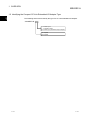
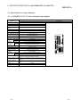
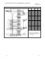
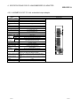
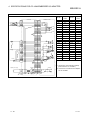
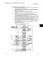
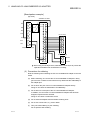
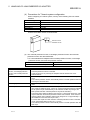
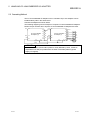
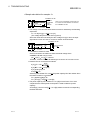
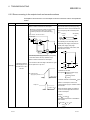
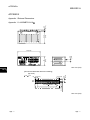
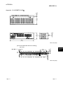
CC-Link Embedded I/O Adapter
,
User s Manual
MODEL
CC-LINK-M-I/O-U-E
MODEL
CODE
13JR59
CC-Link Embedded I/O Adapter
,
User s Manual
SH(NA)-080324E-C(0603)MEE
HEAD OFFICE : TOKYO BUILDING, 2-7-3 MARUNOUCHI, CHIYODA-KU, TOKYO 100-8310, JAPAN
NAGOYA WORKS : 1-14 , YADA-MINAMI 5-CHOME , HIGASHI-KU, NAGOYA , JAPAN
When exported from Japan, this manual does not require application to the
Ministry of Economy, Trade and Industry for service transaction permission.
Specifications subject to change without notice.
Mitsubishi Programmable Logic Controller
MONO
• SAFETY PRECAUTIONS •
(Always read these instructions before using this equipment.)
Before using this product, please read this manual and the relevant manuals introduced in this manual
carefully and pay full attention to safety to handle the product correctly.
The instructions given in this manual are concerned with this product. Refer to the user's manual of the
CPU module to use for a description of the PLC system safety precautions.
In this manual, the safety instructions are ranked as "DANGER" and "CAUTION".
DANGER
Indicates that incorrect handling may cause hazardous conditions,
resulting in death or severe injury.
! CAUTION
Indicates that incorrect handling may cause hazardous conditions,
resulting in medium or slight personal injury or physical damage.
!
Note that the ! CAUTION level may lead to a serious consequence according to the circumstances.
Always follow the instructions of both levels because they are important to personal safety.
Please save this manual to make it accessible when required and always forward it to the end user.
[Design Precautions]
!
DANGER
• When there are communication errors with the data link, the communication error station will
enter the following condition.
Build an interlock circuit into the sequence program to operate system safely by using the
communication state information.
An accident may occur by a false output or a malfunction.
(1) Turn off all input from Remote I/O station.
(2) Turn off all output from Remote I/O station.
• The output may be left ON or OFF due to trouble in the CC-Link embedded I/O adapter.
Configure a circuit to monitor I/O signals which may lead to a serious accident..
!
CAUTION
• Use the CC-Link embedded I/O adapter in an environment that meets the general specifications
contained in this manual.
Using this adapter in an environment outside the range of the general specifications could result
in electric shock, fire, malfunction, and damage to or deterioration of the product.
• Do not bunch the control wires or communication cables with the main circuit or power wires, or
install them close to each other.
They should be installed 100 mm (3.9 in.) or more from each other.
Not doing so could result in noise that would cause malfunction.
A-1
A-1
[Installation Precautions]
!
CAUTION
• Do not directly touch the CC-Link embedded I/O adapter's conductive parts.
Doing so could cause malfunction or failure in the CC-Link embedded I/O adapter.
• Securely solder the CC-Link embedded I/O adapter to install it to a user board.
Defective contact could cause malfunction.
[Wiring Precautions]
!
DANGER
• Before beginning any installation or wiring work, make sure that all phases of the power supply
have been obstructed from the outside.
Failure to completely shut off the power supply phases may cause electric shock and/or damage
to the adapter.
!
CAUTION
• Always ground the FG terminal to the protective ground conductor.
Doing so may cause electric shock or malfunction.
• Correctly connect the CC-Link embedded I/O adapter after confirming the rated voltage and pin
numbers of the product.
Failure to do so could make a short circuit with bare solderless terminals.
• When wiring the CC-Link embedded I/O adapter, check the rated voltage and terminal layout
and make sure the wiring is done correctly.
Connecting a power supply that differs from the rated voltage or wiring it incorrectly may cause
fire, failure or malfunction.
• Make sure that there are no foreign substances such as sawdust or wiring debris inside the CCLink embedded I/O adapter.
Such debris could cause fire, failure or malfunction.
• Make sure that the communication cable connected to the adapter is kept in the duct or fixed
with cramps.
Failure to do so may cause a damage to the user board or cables due to dangling, shifting or
inadvertent handling of cables, or misoperation because of bad cable contacts.
• Do not grab on the cable when removing the communication cable connected to the adapter.
When removing the cable with a connector, hold the connector on the side that is connected to
the adapter.
When removing the cable without a connector, loose the screws on the side that is connected to
the adapter.
Pulling the cable that is still connected to the adapter may cause a damage to the user board or
cable, or malfunction due to bad cable contacts.
A-2
A-2
[Starting and Maintenance Precautions]
!
DANGER
• Do not touch the terminals or connector while the power is on.
Doing so may cause electric shock or malfunction.
• Make sure to switch all phases of the external power supply off before cleaning or re-tightening
the terminal screws.
Failure to do so may damage the CC-Link embedded I/O adapter or cause malfunction.
!
CAUTION
• Do not disassemble or modify the CC-Link embedded I/O adapter.
Doing so could cause failure, malfunction, injury or fire.
• Because the case of the CC-Link embedded I/O adapter is made of resin, be careful not to drop
it or expose it to strong impact.
It may damage the CC-Link embedded I/O adapter.
• Before mounting or dismounting the user board loaded with the CC-Link embedded I/O adapter
to or from an enclosure, always switch power off externally in all phases.
Failure to do so may damage the CC-Link embedded I/O adapter or cause malfunction.
[Disposal Precautions]
!
CAUTION
• When disposing of this product, treat it as industrial waste.
A-3
A-3
REVISIONS
* The manual number is given on the bottom left of the back cover.
Print Date
* Manual Number
May., 2002 SH(NA)-080324E-A First printing
Aug., 2002 SH(NA)-080324E-B Addition
Revision
Section 4.1.2, 4.2.2, Appendix 1.2
Correction
Conformation to the EMC Directive and Low Voltage Instruction,
Section 1.2, 1.3, 1.4, Chapter 2, Section 4.2.1, 4.3.1, 5.1, 5.2
Mar., 2006 SH(NA)-080324E-C Correction
Chapter 3, Section 5.1
Sep., 2006 SH(NA)-080324E-D Addition
Section 6.2.2
Correction
Section 6.2.1
Japanese Manual Version SH-080323-D
This manual confers no industrial property rights or any rights of any other kind, nor does it confer any patent
licenses. Mitsubishi Electric Corporation cannot be held responsible for any problems involving industrial property
rights which may occur as a result of using the contents noted in this manual.
© 2002 MITSUBISHI ELECTRIC CORPORATION
A-4
A-4
INTRODUCTION
Thank you for purchasing the MELSEC-A series PLC.
Before using the equipment, please read this manual carefully to develop full familiarity with the functions
and performance of the A-series PLC you have purchased, so as to ensure correct use.
Please forward a copy of this manual to the end user.
CONTENTS
1 OVERVIEW
1.1
1.2
1.3
1.4
1.5
1- 1 to 1- 5
Features .................................................................................................................................................. 1Identifying the Compact CC-Link Embedded I/O Adapter Type ........................................................... 1Cautionary Notes when Selecting a CC-Link Embedded I/O Adapter.................................................. 1Specification List ..................................................................................................................................... 1About the Generic, Abbreviated and Technical Terms Used in This Manual....................................... 1-
1
2
3
4
4
2 NAMES AND SETTINGS FOR EACH PART
2- 1 to 2- 2
3 SPECIFICATIONS
3- 1 to 3- 2
4 SPECIFICATIONS FOR CC-LINK EMBEDDED I/O ADAPTER
4- 1 to 4- 10
4.1 Specifications for Input Adapters............................................................................................................ 44.1.1 AJ65MBTL1N-16D CC-Link embedded input adapter ................................................................... 44.1.2 AJ65MBTL1N-32D CC-Link embedded input adapter ................................................................... 44.2 Specifications for Output Adapters......................................................................................................... 44.2.1 AJ65MBTL1N-16T CC-Link embedded output adapter ................................................................. 44.2.2 AJ65MBTL1N-32T CC-Link embedded output adapter ................................................................. 44.3 Specifications for Combined Adapters ................................................................................................... 44.3.1 AJ65MBTL1N-16DT CC-Link embedded combined adapter ......................................................... 45 HANDLING CC-Link EMBEDDED I/O ADAPTER
1
1
3
5
5
7
9
9
5- 1 to 5- 7
5.1 Precautionary Notes for Handling and Installation................................................................................. 5- 1
5.2 Cascading Method .................................................................................................................................. 5- 5
5.3 Connection Method of CC-Link Dedicated Cable.................................................................................. 5- 6
6 TROUBLESHOOTING
6- 1 to 6- 5
6.1 Verifying Errors from LED Status ........................................................................................................... 66.2 Examples of Errors for CC-Link Embedded I/O Adapter....................................................................... 66.2.1 Errors occurring in the input circuit and corrective actions ............................................................. 66.2.2 Errors occurring in the output circuit and corrective actions........................................................... 6APPENDIX
1
3
3
5
App- 1 to App- 2
Appendix 1 External Dimensions.............................................................................................................App- 1
Appendix 1.1 AJ65MBTL1N-16 ........................................................................................................App- 1
Appendix 1.2 AJ65MBTL1N-32 ........................................................................................................App- 2
A-5
A-5
About Manuals
The following manuals are also related to this product.
In necessary, order them by quoting the details in the tables below.
Related Manuals
Manual Number
(Model Code)
Manual Name
Control Communication Link System Master/Local Module User's Manual
This manual describes the system configuration, performance specification, function, handling, wiring
and troubleshooting for QJ61BT11
(Sold separately)
CC-Link System Master ( Local Module type AJ61BT11/A1SJ61BT11 User's Manual
This manual describes the system configuration, performance specification, function, handling, wiring
and troubleshooting for AJ61BT11 and A1SJ61BT11.
IB-66721
(13J872)
(Sold separately)
CC-Link System Master ( Local Module type AJ61QBT11/A1SJ61QBT11 User's Manual
This manual describes the system configuration, performance specification, function, handling, wiring
and troubleshooting for AJ61QBT11 and A1SJ61QBT11.
SH-080016
(13JL91)
IB-66722
(13J873)
(Sold separately)
Conformation to the EMC Directive and Low Voltage Instruction
For details on making Mitsubishi PLC conform to the EMC directive and low voltage instruction when
installing it in your product, please see Chapter 3, "EMC Directive and Low Voltage Instruction" of the PLC
CPU User's Manual (Hardware).
The CE logo is printed on the main body of the PLC that conforms to the EMC directive and low voltage
instruction.
By making this product conform to the EMC directive and low voltage instruction, it is not necessary to make
those steps individually.
A-6
A-6
1 OVERVIEW
MELSEC-A
1 OVERVIEW
This manual describes the specifications of the CC-Link embedded I/O adapter used
as the remote I/O station of a Control & Communication Link (hereafter abbreviated to
CC-Link) system.
1.1 Features
The following are the features of the CC-Link embedded I/O adapter.
(1) Device-embedded CC-Link remote I/O
This adapter is a modular remote I/O used as a device-embedded adapter.
(2) Direct installation to user board
Using a pin header as the external interface for adapter power supply,
transmission, I/O signals and others, the adapter can be installed directly to a
user board.
(3) Flexible noise reduction measures
Depending on external noise environment, the user board can be equipped with
a noise filter to enhance noise resistance as necessary.
(4) Insulation method
The adapter power supply uses a transformer insulation method and the external
I/O uses a photocoupler insulation method.
(5) Overload protection function, overvoltage protection function and
overheat protection function
The transistor output section has the overload, overvoltage and overheat
protection functions.
(6) Cascade connection
The CC-Link embedded I/O adapters can be cascaded. Two CC-Link embedded
I/O adapters can be installed side by side within the same board.
User board
DA
DB
DG
SLD
(7) CC-Link Ver. 1.10 compatibility
The CC-Link embedded I/O adapter is compatible with CC-Link Ver. 1.10.
1-1
1-1
1
1 OVERVIEW
MELSEC-A
1.2 Identifying the Compact CC-Link Embedded I/O Adapter Type
1
The following shows how to identify the type of a CC-Link embedded I/O adapter.
AJ65MBTL1N-16DT
D : 24VDC input
T : Transistor output
DT: 24VDC input, transistor output complex
16: 16 points
32: 32 points
1-2
1-2
1 OVERVIEW
MELSEC-A
1.3 Cautionary Notes when Selecting a CC-Link Embedded I/O Adapter
The following explains the cautionary notes and specifications that apply when
selecting a CC-Link embedded I/O adapter for use in the CC-Link system:
(1) This is a embedded I/O adapter designed specifically for the CC-Link system.
Do not connect the adapter to other data-link systems, such as the
MELSECNET/MINI.
(2) 32 points are assigned per station for a CC-Link embedded I/O adapter.
The second-half 16 points of a 16-point CC-Link embedded I/O adapter are empty
but are not usable.
(3) For the maximum switching frequency when driving a load in the CC-Link
embedded output adapter, set to one second or more each for ON and OFF.
(4) When using a counter, a timer or the like that uses a DC/DC converter as the load
for a CC-Link embedded transistor output adapter having a maximum load current
of 0.1A, a rush current flows when the adapter is turned on and at fixed intervals
during operation. For this reason, malfunctions may occur if the average current
is set. When the above load is used, connect resistance or inductance in parallel
to the load, or use an output adapter having a large maximum load current in
order to minimize the effects of the rush current.
Resistance
Load
Output
adapter
Inductance
Load
Output
adapter
(5) When using the AJ65MBTL1N-16D, AJ65MBTL1N-16DT or AJ65MBTL1N-32D
CC-Link embedded I/O adapter, the maximum number of simultaneous input
points listed in the specifications will change, depending on the ambient
temperature.
The maximum number of simultaneous input points is shown in the diagram
below:
Maximum number of simultaneous input points [%]
(a) Dilating curve for the AJ65MBTL1N-16D or AJ65MBTL1N-16DT
[%]
100
50
0
10
20
30
40 45
55
[°C]
Ambient temperature [°C]
1-3
1-3
1 OVERVIEW
MELSEC-A
Maximum number of simultaneous input points [%]
(b) Dilating curve for the AJ65MBTL1N-32D
[%]
100
50
0
10
20
30
40
50 55
[°C]
Ambient temperature [°C]
1.4 Specification List
Specification list for each compact remote I/O adapter is shown below.
Model
Specification
Reference
AJ65MBTL1N-16D
16 points 24VDC positive common (sink) input
Section 4.1.1
AJ65MBTL1N-32D
32 points 24VDC positive common (sink) input
Section 4.1.2
AJ65MBTL1N-16T
16 points transistor output 0.1A sink output
Section 4.2.1
AJ65MBTL1N-32T
32 points transistor output 0.1A sink output
Section 4.2.2
AJ65MBTL1N-16DT
8 points 24VDC positive common (sink) input,
8 points transistor output 0.1A sink output.
Section 4.3.1
1.5 About the Generic, Abbreviated and Technical Terms Used in This Manual
The abbreviated and technical terms used in this manual are listed below:
Generic/abbreviated/
technical term
CC-Link
Master/local module
CC-Link embedded I/O
adapter
Description
Abbreviation of Control & Communications Link
Generic term for the QJ61BT11, AJ61BT11, A1SJ61BT11, AJ61QBT11 and A1SJ61QBT11 CCLink system master/local module
Generic term for the AJ65MBTL1N-
CC-Link embedded I/O adapter
CC-Link embedded input
adapter
Generic term for the AJ65MBTL1N- D CC-Link embedded input adapter
CC-Link embedded output
adapter
Generic term for the AJ65MBTL1N- T CC-Link embedded output adapter
CC-Link embedded combined
Generic term for the AJ65MBTL1N- DT CC-Link embedded combined adapter
adapter
1-4
1-4
1 OVERVIEW
MELSEC-A
MEMO
1-5
1-5
2 NAMES AND SETTINGS FOR EACH PART
MELSEC-A
2 NAMES AND SETTINGS FOR EACH PART
The names and settings for the component of the CC-Link embedded I/O adapter are
shown below.
2
AJ65MBTL1N-16
AJ65MBTL1N-32
1)
1)
3)
3)
2)
2)
4)
4)
No.
1)
Item
Operating status indicator LEDs
Description
LED name
PW
Confirmation details
Turns on when power supply of CC-Link embedded I/O
adapter is turned on.
Checks if the input adapter is communicating with the
L RUN
master station of CC-Link embedded I/O adapter normally.
Turns on when normal data is received from master
station, and turns off when time has expired.
On: Communication data error.
Flicker at regular intervals:
Indicates that the station number setting or
transmission speed setting switch position was
L ERR
changed while power is on.
Flicker at irregular intervals:
Indicates that the terminal resistor is left unconnected
or that the CC-Link embedded I/O adapter or CC-Link
dedicated cable is affected by noise.
Off: Normal communication.
X0 to XF/X0 to X1F Shows on/off status of I/O.
Y0 to YF/Y0 to Y1F Lit when on, unlit when off.
2-1
2-1
2 NAMES AND SETTINGS FOR EACH PART
No.
2)
MELSEC-A
Item
Description
Transmission speed setting
Setting switch status
4
2
1
Transmission
speed
0
OFF
OFF
OFF
156 kbps
1
OFF
OFF
ON
625 kbps
2
OFF
ON
OFF
2.5 Mbps
3
OFF
ON
ON
5.0 Mbps
4
ON
OFF
OFF
10 Mbps
Setting value
2
Be sure to set the transmission speed within the above range.
3)
Station number setting switches
Select "10," "20" or "40" to set the ten's place of the station number.
Select "1," "2," "4" or "8" to set the one's place of the station number.
Always set the station number within the range of 1 to 64.
1 Duplicate station number cannot be set.
Station
number
40
Ten's place
20
10
8
One's place
4
2
1
1
2
OFF
OFF
OFF
OFF
OFF
OFF
OFF
OFF
OFF
OFF
OFF
ON
ON
OFF
3
4
OFF
OFF
OFF
OFF
OFF
OFF
OFF
OFF
OFF
OFF
ON
OFF
OFF
:
10
:
OFF
:
OFF
:
ON
:
OFF
:
OFF
:
OFF
:
OFF
11
:
OFF
:
OFF
:
ON
:
OFF
:
OFF
:
OFF
:
ON
:
64
ON
ON
OFF
OFF
ON
OFF
OFF
(Example) Set the switches as below when setting the station number to 32:
4)
External I/F pin header
Station
number
40
Ten's place
20
10
8
One's place
4
2
1
32
OFF
ON
ON
OFF
OFF
ON
OFF
Pin header for connection of the adapter power supply, communication line,
I/O power supply, external supply power, and input/output signals (refer to
Chapter 4 for the pin numbers.)
2-2
2-2
3 SPECIFICATIONS
MELSEC-A
3 SPECIFICATIONS
This section explains the CC-Link embedded I/O adapter general specifications.
Table 3.1 General specifications
Item
3
Specifications
Operating ambient
temperature
Storage ambient
temperature
Operating ambient
humidity
Storage ambient
humidity
Vibration
resistance
Shock resistance
Operating
environment
Operating height
Installation area
Over-voltage
category 1
Pollution rate 2
0 to 55 °C
-20 to 75 °C
10 to 90 % RH, No condensation
10 to 90 % RH, No condensation
Frequency
Acceleration
Amplitude
Sweep Count
When there is
10 to 57 Hz
—
0.075 mm
Conforming
10 times
intermittent
2
to JIS B
9.8 m/s
—
57 to 150 Hz
each in X, Y
vibration
3502, IEC
and Z axis
10 to 57 Hz
—
0.035 mm
When there is
61132-2
(80 minutes)
continuous
2
4.9 m/s
—
57 to 150 Hz
vibration
2
Conforming to JIS B 3502, IEC 61131-2 (147 m/s , 3 times each in 3 directions)
No corrosive gas present
2000 m(6562 ft) or less
3
On the control board
II or less
2 or less
1 Indicates the location where the device is connected from the public cable network to the
device structure wiring area.
Category II applies to the devices to which the power is supplied from a fixed equipment.
Surge withstand voltage for devices with up to 300 V of rated voltage is 2500 V.
2 This is an index which indicates the degree of conductive object generation in the
environment Pollution level 2 is when only non-conductive pollution occurs.
A temporary conductivity caused by condensation must be expected occasionally.
3 Do not use or store the PLC in the environment where the pressure is higher than the
atmospheric pressure at sea level. Otherwise, malfunction may result. To use the PLC in
high-pressure environment, contact your nearest Mitsubishi representative.
3-1
3-1
3 SPECIFICATIONS
MELSEC-A
MEMO
3
3-2
3-2
4 SPECIFICATIONS FOR CC-LINK EMBEDDED I/O ADAPTER
MELSEC-A
4 SPECIFICATIONS FOR CC-LINK EMBEDDED I/O ADAPTER
4.1 Specifications for Input Adapters
4.1.1 AJ65MBTL1N-16D CC-Link embedded input adapter
Form
Specification
Number of input points
Isolation method
Surface shape
16 points
Photocoupler
Rated input voltage
24V DC
Rated input current
Approx. 4mA
Operating voltage range
4
DC input adapter
AJ65MBTL1N-16D
19.2 to 26.4V DC
(ripple ratio: within 5%)
Max. simultaneous ON
input points
50% (See section 1.3)
ON voltage/ON current
18V or higher/3.5mA or higher
OFF voltage/OFF current
Input resistance
6V or lower/1.7mA or lower
Approx. 5.1kΩ
Response
OFF
ON
1.5ms or lower (at 24V DC)
time
ON
OFF
1.5ms or lower (at 24V DC)
Input type
Positive common (sink)
Wiring method for common
CC-Link station type
Number of occupied stations
I/O adapter
Voltage
power supply
Current
Noise durability
16 points/1 common
Remote I/O station
1 station 32 points assignment (use 16 points)
20.4 to 26.4V DC (ripple rate: within 5%)
35mA or lower (at 24V DC)
DC type noise voltage 500Vp-p, noise width 1μs, noise carrier
frequency 25 to 60Hz (noise simulator condition)
Dielectric withstand voltage 500V AC for 1 minute between all DC external terminals and
ground
Insulation resistance
Weight
External wiring system
4-1
10MΩ or higher, measured with a 500V DC insulation resistance
tester
0.03kg
44-pin, 2-row, 2mm-pitch pin header
4-1
4 SPECIFICATIONS FOR CC-LINK EMBEDDED I/O ADAPTER
MELSEC-A
External connection
Signal
name
Circuit board
Pin No. Singnal
name
DA
B22
DA
DB
A22
DB
DG
B21
DG
SLD
A21
FG
B20
OE-OUT
A20
OE-IN
B19
SD-OUT
A19
SD-IN
2
RD
A18
RDGON
Empty
B17
Pin No.
Signal
name
Link
IC
B22
DA
A22
DB
B21
DG
A21
FG
B20
OE-OUT
A20
OE-IN
To G/A
To G/A
B19
SD-OUT
A19
SD-IN
B18
RD
A18
RDGON
To G/A
B17
Empty
A17
GND
B16
Empty
A16
Empty
B15
Empty
A15
Empty
B14
X0
A14
X1
B13
X2
A13
X3
B12
X4
A12
X5
B11
X6
A11
X7
B10
X8
A10
X9
A17
GND
B16
Empty
A16
Empty
B15
Empty
A15
Empty
X0
B14
X0
X1
A14
X1
X2
B13
X2
X3
A13
X3
X4
B12
X4
B09
XA
A09
XB
X5
A12
X5
X6
B11
X6
B08
XC
A08
XD
X7
A11
X7
X8
B10
X8
X9
A10
X9
XA
B09
XA
XB
A09
XB
XC
B08
XC
XD
A08
XD
XE
B07
XE
XF
A07
COM
B06
24V DC
22000pF
630V
Adapter power supply
+24V
24G
FG
4-2
B18
Signal
name
Pin No.
AJ65MBTL1N-16D
1
R
R
B07
XE
A07
XF
B06
COM
A06
COM
B05
Empty
A05
Empty
B04
Empty
A04
Empty
B03
Empty
A03
Empty
XF
B02
+ 24V
A02
+ 24V
COM
B01
24G
A01
24G
A06
COM
B05
Empty
A05
Empty
B04
Empty
A04
Empty
B03
Empty
A03
Empty
B02
+24V
A02
+24V
B01
24G
A01
24G
R
R
Insulation
DC/DC
1: Add circuit for noise reduction capability.
(Refer to Section 5.1 for details.)
2: Connect A17 and A18 when the adapters
are not cascaded.
4-2
4
4 SPECIFICATIONS FOR CC-LINK EMBEDDED I/O ADAPTER
MELSEC-A
4.1.2 AJ65MBTL1N-32D CC-Link embedded input adapter
Form
Specification
DC input adapter
AJ65MBTL1N-32D
Number of input points
Isolation method
Surface shape
32 points
Photocoupler
Rated input voltage
24V DC
Rated input current
Approx. 4mA
Operating voltage range
19.2 to 26.4V DC
(ripple ratio: within 5%)
Max. simultaneous ON
input points
50% (See section 1.3)
ON voltage/ON current
18V or higher/3.5mA or higher
OFF voltage/OFF current
Input resistance
6V or lower/1.7mA or lower
Approx. 5.1kΩ
Response
OFF
ON
1.5ms or lower (at 24V DC)
time
ON
OFF
1.5ms or lower (at 24V DC)
Input type
Positive common (sink)
Wiring method for common
CC-Link station type
Number of occupied stations
I/O adapter
Voltage
power supply
Current
Noise durability
32 points/1 common
Remote I/O station
1 station 32 points assignment (use 32 points)
20.4 to 26.4V DC (ripple rate: within 5%)
45mA or lower (at 24V DC)
DC type noise voltage 500Vp-p, noise width 1μs, noise carrier
frequency 25 to 60Hz (noise simulator condition)
Dielectric withstand voltage 500V AC for 1 minute between all DC external terminals and
ground
Insulation resistance
Weight
External wiring system
4-3
10MΩ or higher, measured with a 500V DC insulation resistance
tester
0.04kg
62-pin, 2-row, 2mm-pitch pin header
4-3
4 SPECIFICATIONS FOR CC-LINK EMBEDDED I/O ADAPTER
MELSEC-A
External connection
Signal
name
Circuit board
Pin No.
Signal
name
DA
B31
DA
DB
A31
DB
DG
B30
DG
SLD
A30
FG
B29
OE-OUT
A29
OE-IN
2
24V DC
SD-OUT
A28
SD-IN
B27
RD
A27
RDGON
Empty
B26
Pin No.
Signal
name
B31
DA
A31
DB
B30
DG
A30
FG
B29
OE-OUT
A29
OE-IN
To G/A
B28
SD-OUT
A28
SD-IN
To G/A
B27
RD
A27
RDGON
Link
IC
To G/A
Pin No.
B26
Empty
A26
GND
B25
Empty
A25
Empty
B24
Empty
A24
Empty
B23
X0
A23
X1
B22
X2
A22
X3
B21
X4
A21
X5
B20
X6
A20
X7
B19
X8
A19
X9
A26
GND
B25
Empty
A25
Empty
B24
Empty
A24
Empty
X0
B23
X0
X1
A23
X1
X2
B22
X2
X3
A22
X3
X4
B21
X4
B18
XA
A18
XB
X5
A21
X5
X6
B20
X6
B17
XC
A17
XD
X7
A20
X7
X8
B19
X8
R
R
B16
XE
A16
XF
B15
X10
A15
X11
X9
A19
X9
XA
B18
XA
B14
X12
A14
X13
XB
A18
XB
XC
B17
XC
B13
X14
A13
X15
XD
A17
XD
B12
X16
A12
X17
XE
B16
XE
B11
X18
A11
X19
XF
A16
XF
X10
B15
X10
X11
A15
X11
B10
X1A
A10
X1B
X12
X13
B14
X12
B09
X1C
A09
X1D
A14
X13
X14
B13
X14
B08
X1E
A08
X1F
X15
A13
X15
B07
COM
A07
COM
X16
B12
X16
X17
A12
X17
B06
Empty
A06
Empty
X18
B11
X18
B05
Empty
A05
Empty
X19
A11
X19
X1A
B10
X1A
B04
Empty
A04
Empty
X1B
A10
X1B
B03
Empty
A03
Empty
X1C
B09
X1C
X1D
A09
X1D
B02
+24V
A02
+24V
X1E
B08
X1E
X1F
A08
X1F
B01
24G
A01
24G
COM
B07
COM
COM
A07
COM
B06
Empty
A06
Empty
B05
Empty
A05
Empty
B04
Empty
A04
Empty
B03
Empty
A03
Empty
B02
+24V
A02
+24V
B01
24G
A01
24G
22000pF
630V
Adapter power supply
+24V
24G
FG
4-4
B28
Signal
name
AJ65MBTL1N-32D
R
R
Insulation
DC/DC
1: Add circuit for noise reduction capability.
(Refer to secton 5.1 for details.)
2: Connect A26 and A27 when the adapters
are not cascaded.
1
4-4
4 SPECIFICATIONS FOR CC-LINK EMBEDDED I/O ADAPTER
MELSEC-A
4.2 Specifications for Output Adapters
4.2.1 AJ65MBTL1N-16T CC-Link embedded output adapter
Form
Specification
Transistor output adapter
AJ65MBTL1N-16T
Number of output points
Isolation method
Surface shape
16 points
Photocoupler
Rated load voltage
12/24V DC
Operating load voltage
range
Max. load current
10.2 to 26.4V DC (ripple ratio: within 5%)
0.1A/point, 1.6A/1 common
Max. inrush current
0.7A 10ms or lower
Leakage current at OFF
0.1mA or lower
Max. voltage drop at ON
0.1V or lower (TYP) 0.1A
0.2V or lower (MAX) 0.1A
Output method
Sink type
Protection functions
Overload, over-voltage and overheat protection
Response
OFF
ON
1ms or lower
time
ON
OFF
1ms or lower (rated load, resistive load)
External
Voltage
10.2 to 26.4V DC (ripple ratio: within 5%)
Power supply
for output
Current
10mA or lower (When all points are ON at 24V DC)
Not including external load current
Surge suppression
Wiring method for common
Zener diode
16 points/1 common
CC-Link station type
Remote I/O station
Number of occupied
stations
1 station 32 points assignment
(use 16 points)
I/O adapter
Voltage
20.4 to 26.4V DC (ripple ratio: within 5%)
power supply
Current
50mA or lower (When all points are ON at 24V DC)
Noise durability
DC type noise voltage 500Vp-p, noise width 1μs, noise carrier
frequency 25 to 60Hz (noise simulator condition)
Dielectric withstand voltage 500V AC for 1 minute between all DC external terminals and
ground
Insulation resistance
Weight
External wiring system
4-5
10MΩ or higher, measured with a 500V DC insulation resistance
tester
0.03kg
44-pin, 2-row, 2mm-pitch pin header
4-5
4 SPECIFICATIONS FOR CC-LINK EMBEDDED I/O ADAPTER
MELSEC-A
External connection
Signal
name
Circuit board
Pin No. Singnal
name
DA
B22
DA
DB
A22
DB
DG
B21
DG
SLD
A21
FG
B20
OE-OUT
A20
OE-IN
B19
SD-OUT
A19
SD-IN
Link
IC
B22
DA
A22
DB
B21
DG
A21
FG
B20
OE-OUT
A20
OE-IN
To G/A
To G/A
B19
SD-OUT
A19
SD-IN
B18
RD
A18
RDGON
Empty
A17
GND
Empty
A16
Empty
B15
Empty
A15
Empty
B14
Y0
A14
Y1
B13
Y2
A13
Y3
B12
Y4
A12
Y5
B11
Y6
A11
Y7
B10
Y8
A10
Y9
Y4
B09
YA
A09
YB
A12
Y5
B11
Y6
B08
YC
A08
YD
Y7
A11
Y7
B07
YE
A07
YF
Y8
B10
Y8
Y9
A10
Y9
B06
CTL+
A06
CTL+
YA
B09
YA
YB
B05
COM-
A05
COM-
A09
YB
YC
B08
YC
B04
Empty
A04
Empty
YD
A08
YD
YE
B07
YE
B03
Empty
A03
Empty
B02
+ 24V
A02
+ 24V
B01
24G
A01
24G
RDGON
B17
Empty
A17
B16
GND
Empty
A16
Empty
B15
Empty
A15
Empty
Y0
B14
Y0
Y1
A14
Y1
Y2
B13
Y2
Y3
A13
Y3
Y4
B12
Y5
Y6
YF
A07
YF
CTL+
B06
CTL+
COM-
A06
CTL+
B05
COM-
22000pF
630V
Adapter power supply
+24V
24G
FG
4-6
Signal
name
B16
RD
A18
L
12/24V DC
Pin No.
B17
B18
2
L
Signal
name
Pin No.
AJ65MBTL1N-16T
1
A05
COM-
B04
Empty
A04
Empty
B03
Empty
A03
Empty
B02
+24V
A02
+24V
B01
24G
A01
24G
To G/A
Constant
voltage
circuit
Insulation
DC/DC
1: Add circuit for noise reduction capability.
(Refer to Section 5.1 for details.)
2: Connect A17 and A18 when the adapters
are not cascaded.
4-6
4 SPECIFICATIONS FOR CC-LINK EMBEDDED I/O ADAPTER
MELSEC-A
4.2.2 AJ65MBTL1N-32T CC-Link embedded output adapter
Form
Specification
Transistor output adapter
AJ65MBTL1N-32T
Number of output points
Isolation method
Surface shape
32 points
Photocoupler
Rated load voltage
12/24V DC
Operating load voltage
range
Max. load current
10.2 to 26.4V DC (ripple ratio: within 5%)
0.1A/point, 3.2A/1 common
Max. inrush current
0.7A 10ms or lower
Leakage current at OFF
0.1mA or lower
Max. voltage drop at ON
0.1V or lower (TYP) 0.1A
0.2V or lower (MAX) 0.1A
Output method
Sink type
Protection functions
Overload, over-voltage and overheat protection
Response
OFF
ON
1ms or lower
time
ON
OFF
1ms or lower (rated load, resistive load)
External
Voltage
10.2 to 26.4V DC (ripple ratio: within 5%)
Power supply
for output
Current
15mA or lower (When all points are ON at 24V DC)
Not including external load current
Surge suppression
Wiring method for common
Zener diode
32 points/1 common
CC-Link station type
Remote I/O station
Number of occupied
stations
1 station 32 points assignment
(use 32 points)
I/O adapter
Voltage
20.4 to 26.4V DC (ripple ratio: within 5%)
power supply
Current
60mA or lower (When all points are ON at 24V DC)
Noise durability
DC type noise voltage 500Vp-p, noise width 1μs, noise carrier
frequency 25 to 60Hz (noise simulator condition)
Dielectric withstand voltage 500V AC for 1 minute between all DC external terminals and
ground
Insulation resistance
Weight
External wiring system
4-7
10MΩ or higher, measured with a 500V DC insulation resistance
tester
0.04kg
62-pin, 2-row, 2mm-pitch pin header
4-7
4 SPECIFICATIONS FOR CC-LINK EMBEDDED I/O ADAPTER
MELSEC-A
External connection
Signal
name
Circuit board
Pin No.
DA
B31
DA
DB
A31
DB
DG
B30
DG
SLD
A30
FG
B29
OE-OUT
A29
OE-IN
B28
SD-OUT
A28
SD-IN
2
L
L
12/24V DC
Adapter power supply
RD
A27
RDGON
Empty
B26
Pin No.
Signal
name
Link
IC
B31
DA
A31
DB
B30
DG
A30
FG
B29
OE-OUT
A29
OE-IN
To G/A
To G/A
B28
SD-OUT
A28
SD-IN
B27
RD
A27
RDGON
To G/A
B26
Empty
A26
GND
B25
Empty
A25
Empty
B24
Empty
A24
Empty
B23
Y0
A23
Y1
Y2
A22
Y3
A26
GND
B25
Empty
A25
Empty
B24
Empty
B22
A24
Empty
Y0
B23
Y0
B21
Y4
A21
Y5
Y1
A23
Y1
B20
Y6
A20
Y7
Y2
B22
Y2
Y3
A22
Y3
B19
Y8
A19
Y9
Y4
B21
Y4
B18
YA
A18
YB
Y5
A21
Y5
Y6
B20
Y6
B17
YC
A17
YD
Y7
A20
Y7
B16
YE
A16
YF
Y8
B19
Y8
Y9
A19
Y9
B15
Y10
A15
Y11
YA
B18
YA
YB
B14
Y12
A14
Y13
A18
YB
YC
B17
YC
B13
Y14
A13
Y15
YD
A17
YD
YE
B16
YE
B12
Y16
A12
Y17
Y18
A11
Y19
YF
A16
YF
B11
Y10
B15
Y10
Y11
A15
Y11
B10
Y1A
A10
Y1B
Y12
Y13
B14
Y12
B09
Y1C
A09
Y1D
A14
Y13
Y14
B13
Y14
B08
Y1E
A08
Y1F
Y15
A13
Y15
B07
CTL+
A07
CTL+
Y16
B12
Y16
Y17
A12
Y17
B06
COM-
A06
COM-
Y18
B11
Y18
B05
COM-
A05
COM-
B04
Empty
A04
Empty
Y19
A11
Y19
Y1A
B10
Y1A
Y1B
A10
Y1B
Y1C
B09
Y1C
B03
Empty
A03
Empty
Y1D
A09
Y1D
B02
+24V
A02
+24V
Y1E
B08
Y1E
Y1F
A08
Y1F
B01
24G
A01
24G
CTL+
B07
CTL+
CTL+
A07
CTL+
COM-
B06
COM-
COM-
A06
COM-
COM-
B05
COM-
COM-
A05
COM-
B04
Empty
A04
Empty
B03
Empty
A03
Empty
B02
+24V
A02
+24V
B01
24G
A01
24G
22000pF
630V
+24V
24G
FG
4-8
B27
Signal
name
Pin No.
AJ65MBTL1N-32T
Signal
name
1
Constant
voltage
circuit
Insulation
DC/DC
1: Add circuit for noise reduction capability.
(Refer to Section 5.1 for details.)
2: Connect A26 and A27 when the adapters
are not cascaded.
4-8
4 SPECIFICATIONS FOR CC-LINK EMBEDDED I/O ADAPTER
MELSEC-A
4.3 Specifications for Combined Adapters
4.3.1 AJ65MBTL1N-16DT CC-Link embedded combined adapter
Form
DC input transistor output combined adapter
Specification
AJ65MBTL1N-16DT
Input specification
Number of input points
8 points
Isolation method
Number of output points
Photocoupler
Rated input voltage
24V DC
Rated input current
Approx. 7mA
Operating voltage range
8 points
Isolation method
Photocoupler
Rated load voltage
24V DC
Operating load voltage range
19.2 to 26.4V DC
(ripple ratio: within 5%)
19.2 to 26.4V DC(ripple ratio: within 5%)
Max. load current
Max. simultaneous input
points
50% (See section 1.3)
ON voltage/ON current
14V or higher/3.5mA or higher
OFF voltage/OFF current
Surface shape
Output specification
0.1A/point
0.8A/common
Max. inrush current
6V or lower/1.7mA or lower
0.7A 10ms or lower
Leakage current at OFF
0.1mA or lower
Max. voltage drop at ON
0.1V or lower (TYP)0.1A
0.2V or lower (MAX)0.1A
Input resistance
Output type
A pprox. 3.3k Ω
Response time OFF
ON
ON
OFF
Sink type
Protection functions
1.5ms or lower (at 24V DC)
1.5ms or lower (at 24V DC)
Overload, over-voltage and overheat
protection
Response
time
OFF
ON
1ms or lower
ON
OFF
1ms or lower
(rated load, resistive load)
External
Voltage
Power supply Current
for output
Input type
Positive common (Sink type)
Wiring method for common
CC-Link station type
Number of occupied stations
19.2 to 26.4V DC (ripple ratio: within 5%)
5mA or lower
(When all points are ON at 24V DC)
Not including external load current
Surge suppression
Zener diode
16 points/1 common
Remote I/O station
1 station 32 points assignment (use 16 points)
I/O adapter
Voltage
20.4 to 26.4V DC(ripple ratio: within 5%)
power supply
Current
50mA or lower (when all points are ON at 24V DC) Not including external load current
Noise durability
DC type noise voltage 500Vp-p, noise width 1μs, noise carrier frequency 25 to 60Hz(noise
simulator condition)
Dielectric withstand voltage 500V AC for 1 minute between all DC external terminals and ground
Insulation resistance
Weight
External wiring system
4-9
10MΩ or higher, measured with a 500V DC insulation resistance tester between all DC external
terminals and ground
0.03kg
44-pin, 2-row, 2mm-pitch pin header
4-9
4 SPECIFICATIONS FOR CC-LINK EMBEDDED I/O ADAPTER
MELSEC-A
External connection
Signal
name
Pin No.
Signal
name
B22
DA
A22
DB
B21
DG
A21
FG
B20
OE-OUT
A20
OE-IN
B19
SD-OUT
A19
SD-IN
B18
RD
A18
RDGON
Pin No.
Signal
name
Circuit board
Pin No. Singnal
name
DA
B22
DA
DB
A22
DB
DG
B21
DG
SLD
A21
FG
B20
OE-OUT
2
L
L
24V DC
OE-IN
B19
SD-OUT
A19
SD-IN
B18
RD
A18
RDGON
B17
Empty
A17
GND
B16
Empty
A16
Empty
B15
Empty
A15
Empty
X0
B14
X0
X1
A14
X1
X2
B13
X2
X3
A13
X3
X4
B12
X4
X5
A12
X5
X6
B11
X6
X7
A11
X7
Y8
B10
Y8
Y9
A10
Y9
YA
B09
YA
YB
A09
YB
YC
B08
YC
YD
A08
YD
YE
B07
YE
YF
A07
YF
24V DC
B06
24V DC
24G DC
A06
24V DC
B05
24G DC
A05
24G DC
22000pF
630V
Adapter power supply
+24V
24G
FG
4 - 10
A20
1
B04
Empty
A04
Empty
B03
Empty
A03
Empty
B02
+24V
A02
+24V
B01
24G
A01
24G
AJ65MBTL1N-16DT
Link
IC
To G/A
To G/A
To G/A
R
R
R
R
B17
Empty
A17
GND
B16
Empty
A16
Empty
B15
Empty
A15
Empty
B14
X0
A14
X1
B13
X2
A13
X3
B12
X4
A12
X5
B11
X6
A11
X7
B10
Y8
A10
Y9
B09
YA
A09
YB
B08
YC
A08
YD
B07
YE
A07
YF
B06
24V DC
A06
24V DC
B05
24G DC
A05
24G DC
B04
Empty
A04
Empty
B03
Empty
A03
Empty
B02
+ 24V
A02
+ 24V
B01
24G
A01
24G
Constant
voltage
circuit
Insulation
DC/DC
1: Add circuit for noise reduction capability.
(Refer to Section 5.1 for details.)
2: Connect A17 and A18 when the adapters
are not cascaded.
4 - 10
5 HANDLING CC-LINK EMBEDDED I/O ADAPTER
MELSEC-A
5 HANDLING CC-Link EMBEDDED I/O ADAPTER
5.1 Precautionary Notes for Handling and Installation
The precautionary notes when handling and installing the CC-Link embedded I/O
adapter for the CC-Link system are described below.
DANGER
• Do not touch the terminals or connector while the power is on.
Doing so may cause electric shock or malfunction.
CAUTION
• Make sure that there are no foreign substances such as sawdust or wiring debris
inside the CC-Link embedded I/O adapter.
Such debris could cause fire, failure or malfunction.
• Do not disassemble or modify the CC-Link embedded I/O adapter.
Doing so could cause failure, malfunction, injury or fire.
• Do not directly touch the CC-Link embedded I/O adapter's conductive parts.
Doing so could cause malfunction or failure in the CC-Link embedded I/O adapter.
• Because the case of the CC-Link embedded I/O adapter is made of resin, be careful
not to drop it or expose it to strong impact.
It may damage the CC-link embedded I/O adapter.
• When disposing of this product, treat it as industrial waste.
• Use the CC-Link embedded I/O adapter in an environment that meets the general
specifications contained in this manual.
Using this adapter in an environment outside the range of the general specifications
could result in electric shock, fire, malfunction, and damage to or deterioration of the
product.
• Before mounting or dismounting the user board loaded with the CC-Link embedded
I/O adapter to or from an enclosure, always switch power off externally in all
phases.
Failure to do so may damage the CC-Link embedded I/O adapter or cause
malfunction.
5
(1) Restrictions on close installation
Because of heat generation, do not install the CC-Link embedded I/O adapters
closely to each other.
Install the CC-Link embedded I/O adapters at least 5mm away from each other.
User board
5mm or more
5-1
5-1
5 HANDLING CC-LINK EMBEDDED I/O ADAPTER
MELSEC-A
(2) Precautions for external wiring
Note the following when designing the user board side circuit and board patterns.
1) Use a user board of 1.6mm thickness.
2) When the noise immunity must be increased, insert a noise filter (FDK
make: NFR5UI203MB or equivalent) and Y capacitor (22000pF 630V) in the
adapter power supply line.
3) Connect the transmission SLD and FG within the board.
As a pattern, connect SLD and FG as near as possible to the external I/O
terminals.
4) Make the transmission patterns (DA, DB) as short as possible.
Design the patterns so that the capacitance is 20pF or less with the CC-Link
embedded I/O adapter mounted on the board. (Guidelines: Pattern length
5cm or less, pattern width 0.18mm or less)
5) Since the cascade communication signal pins (16-point adapter: A17 to A20
pins and B17 to B20 pins, 32-point adapter: A26 to A29 pins and B26 to B29
pins) are susceptible to noise, keep them as far away as possible from the
other patterns (power supply, I/O signal) that include noise.
6) When the adapters are not cascaded, always connect GND and RDGON
(16-point adapter: A17 pin and A18 pin, 32-point adapter: A26 pin and A27
pin) on the board side.
7) Wire the FG pattern so that it does not cross the I/O patterns on the front
and back sides of the board.
Doing so makes the adapter sensitive to noise.
(Example: AJ65MBTL1N-16DT)
Signal
name
User board 1)
4)
Pin No. Singnal
name
DA
B22
DA
DB
A22
DB
DG
B21
DG
SLD
A21
FG
B20
OE-OUT
A20
OE-IN
B19
SD-OUT
A19
SD-IN
5)
6)
L
L
24V DC
RD
A18
RDGON
B17
Empty
A17
GND
B16
Empty
A16
Empty
B15
Empty
A15
Empty
X0
B14
X0
X1
A14
X1
X2
B13
X2
X3
A13
X3
X4
B12
X4
X5
A12
X5
X6
B11
X6
X7
A11
X7
Y8
B10
Y8
Y9
A10
Y9
YA
B09
YA
YB
A09
YB
YC
B08
YC
YD
A08
YD
YE
B07
YE
YF
A07
YF
24V DC
B06
24V DC
24G DC
A06
24V DC
B05
24G DC
A05
24G DC
B04
Empty
A04
Empty
B03
Empty
A03
Empty
B02
+24V
A02
+24V
B01
24G
A01
24G
7)
22000pF
630V
Adapter power supply
+24V
24G
FG
5-2
B18
2)
5
AJ65MBTL1N-16DT
Link
IC
To G/A
To G/A
To G/A
R
R
R
R
Constant
voltage
circuit
Insulation
DC/DC
3)
5-2
5 HANDLING CC-LINK EMBEDDED I/O ADAPTER
MELSEC-A
[Board pattern example]
(top view)
AJ65MBTL1N-16DT
B22 A22
DA
DB
DG
SLD
I/O connector
FG
+24V
24G
Adapter power supply
I/O power supply
24VDC
B01 A01
24GDC
: When using a multi-layer board, eliminate the inner layers to prevent the
capacitance between DA and DB from increasing.
(3) Precautions for soldering
Note the following when soldering the CC-Link embedded I/O adapter to the user
board.
(a) Before soldering, do not store the CC-Link embedded I/O adapter in dusty,
gas-corrosive or similar environment that may deteriorate the solderability of
the adapter pins.
(b) Do not touch the pins of the CC-Link embedded I/O adapter directly.
Doing so can cause the deterioration of solderability.
(c) Do not bend or cut the pins of the CC-Link embedded I/O adapter.
In addition, do not use the CC-Link embedded I/O adapter that has been
dropped, impacted and/or stressed.
Doing so can cause a malfunction or like.
(d) Do not clean the adapter before and after soldering work.
(e) Do not use corrosive flux, e.g. acid or alkali.
(f)
5-3
Carry out hand soldering or post soldering.
Do not perform flow soldering.
5-3
5 HANDLING CC-LINK EMBEDDED I/O ADAPTER
MELSEC-A
(4) Precautions for T-branch system configuration
When configuring a T-branch system, use any of the following CC-Link master
modules.
Module type
QJ61BT11
AJ61BT11
AJ61QBT11
A1SJ61BT11
A1SJ61QBT11
Hardware version
All versions usable
D or later
D or later
E or later
E or later
Confirm the module version as shown below.
Software version
Hardware version
(5) The overload protection function, overvoltage protection function and overheat
protection function are described below.
• CC-Link embedded I/O adapters with overload protection function, overvoltage
protection function and overheat protection function
CC-Link embedded output adapter
AJ65MBTL1N-16T, AJ65MBTL1N-32T
CC-Link embedded combined adapter
AJ65MBTL1N-16DT
Function
Common to overload protection
function, overvoltage protection
function and overheat protection
function
Overload protection function
Overvoltage protection function
Overheat protection function
5-4
Description
1. When overcurrent due to an overload continues to exist, this generates heat and the
overheat protection function is activated.
2. These functions are for protecting the adapters' internal elements but not for
external devices.
1. The overload protection function is activated in a load condition of 1 A to 3 A per
point.
2. The overload protection function automatically returns to normal operation when the
load drops to the rated value.
1. This function protects elements from an abrupt surge caused when a coil load is
used.
1. The overheat protection function works in two-point units.
(The points are paired as Y0/Y1, Y2/Y3, etc., and the overheat protector is activated
for two points in a pair simultaneously. If the overheat condition is prolonged, the
heat spreads and other overheat protectors may also be activated.)
2. The actual output voltage oscillates in the range of 0 V to the load voltage only if the
output is ON when the overheat protection function was activated. In this case, the
average voltage during oscillation with the load voltage of 24 V is approximately 7 V.
(No oscillation occurs when the output is OFF.)
To ensure that output turns OFF when the overheat protection function is activated,
use an external load that turns OFF at 7 V or more.
3. The overheat protection function automatically returns to normal operation when the
heat drops.
5-4
5 HANDLING CC-LINK EMBEDDED I/O ADAPTER
MELSEC-A
5.2 Cascading Method
The CC-Link embedded I/O adapters can be cascaded. Up to two adapters can be
installed side by side in the same board.
Cascade the adapters as shown below.
The following diagram gives an example of 16-point CC-Link embedded I/O adapters.
Review the pin numbers when 32-point CC-Link embedded I/O adapters are used.
OE-IN
A20
OE-IN
B20
A20
OE-OUT
B22
DA
CC-Link enbedded
I/O adapter (2)
SD-IN
RD
A19
A22
DB
B21
DG
A21
FG
B18
A18
RDGON
A17
GND
B19
SD-OUT
SD-IN A19
RD
CC-Link enbedded
I/O adapter (1)
B18
A18
RDGON
A17
GND
B20
OE-OUT
B22
DA
A22
DB
B21
DG
A21
FG
DA
DB
DG
SLD
B19 SD-OUT
FG
(OPEN)
POINT
Since the cascade communication pattern is easily affected by noise, it must be
separated as far away as possible from the other noise-laden patterns (power
supply, I/O signals).
5-5
5-5
5 HANDLING CC-LINK EMBEDDED I/O ADAPTER
MELSEC-A
5.3 Connection Method of CC-Link Dedicated Cable
The procedure for connecting the master adapter and I/O adapter CC-Link dedicated
cable is shown below.
DANGER
• Before beginning any installation or wiring work, make sure all phases of the power
supply have been obstructed from the outside.
Failure to completely shut off the power supply phases may cause electric shock
and/or damage to the adapter.
• Make sure to switch all phases of the external power supply off before cleaning or
re-tightening the terminal screws.
Failure to do so may damage the CC-Link embedded I/O adapter or cause
malfunction.
CAUTION
• Do not bunch the control wires or communication cables with the main circuit or
power wires, or install them close to each other.
They should be installed 100 mm (3.9 in.) or more from each other.
Not doing so could result in noise that would cause malfunction.
• Always ground the FG terminal to the protective ground conductor.
Doing so may cause electric shock or malfunction.
• Securely solder the CC-link embedded I/O adapter to install it to a user board.
Defective contact could cause malfunction.
• Make sure that the communication cable connected to the adapter is kept in the
duct or fixed with cramps.
Failure to do so may cause a damage to the user board or cables due to dangling,
shifting or inadvertent handling of cables, or misoperation because of bad cable
contacts.
• Do not grab on the cable when removing the communication cable connected to the
adapter.
When removing the cable with a connector, hold the connector on the side that is
connected to the adapter.
When removing the cable without a connector, loose the screws on the side that is
connected to the adapter.
Pulling the cable that is still connected to the adapter may cause a damage to the
user board or cable, or malfunction due to bad cable contacts.
5-6
5-6
5 HANDLING CC-LINK EMBEDDED I/O ADAPTER
MELSEC-A
(1) The procedure for connecting the master module and I/O adapter is shown below:
Terminal
resistor
(Blue)
Master module
NC
DA
NC
(White)
User board
DB
User board
NC
(Yellow)
DG
NC
SLD
NC
FG
DA
DB
DG
SLD
FG
DA
DB
DG
SLD
FG
Terminal
resistor 1
CC-Link dedicated cable
2
1 Connect the terminal resistor to the compact remote I/O adapter terminating
station in the locations shown below:
(The terminal resistor is provided with the master module.)
DA
DB
DG
SLD
FG
Terminal resistor
2 Use the CC-Link dedicated cables in the CC-Link system.
If the cables other than the CC-Link dedicated cables are used, we cannot
guarantee the performance of the CC-Link system.
Refer to the CC-Link Partner Association Home Page: http://www.cc-link.org/ for
the specifications and contact information of the CC-Link dedicated cables.
5-7
5-7
6 TROUBLESHOOTING
MELSEC-A
6 TROUBLESHOOTING
6.1 Verifying Errors from LED Status
Power supply
The following table lists causes and corrective actions for errors indicated by LEDs on
the CC-Link embedded I/O adapter when the SW, M/S and PRM LEDs are all off (i.e.
the master module is set properly) in the system configuration example shown below.
CPU
Master
module
Station number 1
Station number 2
Station number 3
CC-Link embedded
I/O adapter A
CC-Link embedded
I/O adapter B
CC-Link embedded
I/O adapter C
LED status
Master
module
TIME
LINE
or
TIME
LINE
CC-Link embedded I/O adapter
Cause
Corrective action
Normal
—
A
B
C
PW
L RUN
L ERR
PW
L RUN
L ERR
PW
L RUN
L ERR
PW
L RUN
L ERR
PW
L RUN
L ERR
PW
L RUN
L ERR
Check the voltage of the 24 V power supply,
Since the LEDs on the CC-Link
embedded I/O adapter A are all off, the and supply the proper power to the CC-Link
24 V power is not supplied or voltage is embedded I/O adapter.
low.
PW
L RUN
L ERR
PW
L RUN
L ERR
PW
L RUN
L ERR
The CC-Link embedded I/O adapter A
is malfunctioning and the LEDs are
unstable (all lights are off, in many
cases).
PW
L RUN
L ERR
PW
L RUN
L ERR
PW
L RUN
L ERR
Identify the disconnected point by referring to
The L RUN lights on the CC-Link
the LED status, and correct it.
embedded I/O adapter B and beyond
are off, indicating the transmission cable
between the CC-Link embedded I/O
adapter A and B has been disconnected
or removed from the terminal block.
PW
L RUN
L ERR
PW
L RUN
L ERR
PW
L RUN
L ERR
The transmission cable is shorted.
Find the shorted cable among the three
transmission cables and repair it.
PW
L RUN
L ERR
PW
L RUN
L ERR
PW
L RUN
L ERR
The transmission cable is wired
incorrectly.
Check the wiring on the terminal block of the
user board and correct the incorrect wiring.
The transmission patterns have been
connected incorrectly.
Check the transmission patterns on the user
board and correct the incorrectly connected
portions.
PW
L RUN
L ERR
PW
L RUN
L ERR
PW
L RUN
L ERR
Restart the power supply after the overlapped
The L RUN lights on the CC-Link
embedded I/O adapters A and C are off, station numbers for the CC-Link embedded I/O
indicating the station numbers for A and adapters are corrected.
C are overlapping.
Exchange the CC-Link embedded I/O adapter.
: lit,
6-1
: unlit,
: flashing,
: lit, flashing or unlit
6-1
6
6 TROUBLESHOOTING
MELSEC-A
LED status
Master
module
TIME
LINE
or
TIME
LINE
6
TIME
LINE
or
TIME
LINE
CC-Link embedded I/O adapter
Cause
Corrective action
A
B
C
PW
L RUN
L ERR
PW
L RUN
L ERR
PW
L RUN
L ERR
Restart the power supply after the transmission
The L RUN light on the CC-Link
embedded I/O adapter B is off, indicating speed is set correctly.
the transmission speed setting for CCLink embedded I/O adapter B is invalid
within the setting range (0 to 4).
PW
L RUN
L ERR
PW
L RUN
L ERR
PW
L RUN
L ERR
The L ERR of the CC-Link embedded Return the setting switch of the CC-Link
embedded I/O adapter to the original position.
I/O adapter C is flashing at fixed
intervals, indicating the setting switch for
CC-Link embedded I/O adapter C has
been changed during normal operation.
PW
L RUN
L ERR
PW
L RUN
L ERR
PW
L RUN
L ERR
The L RUN of the CC-Link embedded Correct the setting switch of the CC-Link
embedded I/O adapter, and restart the power
I/O adapter A is off and L ERR of the
same CC-Link embedded I/O adapter is supply.
lit, indicating the setting switch for CCLink embedded I/O adapter A is set out
of range (transmission speed: 5 to 9,
station number: 65 or greater).
PW
L RUN
L ERR
PW
L RUN
L ERR
PW
L RUN
L ERR
The L ERR of the CC-Link embedded
I/O adapter B is lit, indicating that CCLink embedded I/O adapter B is being
affected by noise. (L RUN may be off.)
Correctly perform grounding of the FGs for the
master module and all CC-Link embedded I/O
adapters.
PW
L RUN
L ERR
PW
L RUN
L ERR
PW
L RUN
L ERR
The L ERR lights on the CC-Link
embedded I/O adapter B and beyond
are lit, indicating the transmission cable
is affected by noise in the area between
CC-Link embedded I/O adapters A and
B. (L RUN may be off.)
Verify the grounding of the SLD of the
transmission cable.
Separate the wire from the power cable as
much as possible (100 mm (3.94 in.)or more).
PW
L RUN
L ERR
PW
L RUN
L ERR
PW
L RUN
L ERR
A terminal resistor is not attached.
(L RUN may be off.)
Check if a terminal resistor is attached.
: lit,
6-2
: unlit,
: flashing,
: lit, flashing or unlit
6-2
6 TROUBLESHOOTING
MELSEC-A
6.2 Examples of Errors for CC-Link Embedded I/O Adapter
This section explains examples of errors that occur in the input circuit, and the
appropriate corrective actions.
6.2.1 Errors occurring in the input circuit and corrective actions
Examples of errors that occur in the input circuit and corrective actions are explained
below:
Error status
Example 1 Input signals do not turn off.
Cause
Corrective action
• Activation via the LED display switch.
• Connect a resistor so that the voltage
between the input terminal and COM1
DC input (sink)
becomes lower than the OFF voltage.
DC input (sink)
Leakage current
CC-Link
embedded
Input
adapter
Resistor
CC-Link
embedded
Input
adapter
A calculation example used to obtain the
resistance value to be connected is shown
on the following page.
Example 2 Input signals do not turn off.
• Sneak path due to the use of two power
supplies.
DC input
E1
E2
E1 > E2
6-3
• Reduce the number of power supplies
from two to one.
• Connect a diode to prevent sneak path.
(as below)
CC-Link
DC input
embedded
Input
adapter
CC-Link
embedded
E2
E1
Input
adapter
6-3
6 TROUBLESHOOTING
MELSEC-A
<Sample calculation for example 1>
AJ65MBTL1N-16D
CC-Link
embedded
input
adapter
Leakage 2.45 mA
current
4.7 k
When a 2.45 mA leakage current flows due
to a switch with LED indicator connected to
the AJ65MBTL1N-16D.
24 V DC
• The voltage VTB across the terminal and common is obtained by the following
expression.
VTB = 2.45 [mA] 5.1 [k ] = 12.5 [V]
(The voltage drop across the LED is ignored.)
Since this result does not satisfy the OFF voltage of 6 [V] or less, the input
signal does not turn off. Hence, connect a resistor as shown below.
AJ65MBTL1N-16D
Current I
4.7 k
R
Input impedance
5.1 k
24 V DC
• Calculation of resistor R value
Current I should be as follows so that the terminal voltage of the
AJ65MBTL1N-16D is 6 [V] or less.
(24 6 [V] ) 4.7 [k ] = 3.83 mA
Therefore, connect a resistor R that will give a current I of 3.83 mA or more.
• Resistor R to be connected is as follows.
6 [V]
6 [V] R > 3.83
5.1 [k ]
6 [V] R > 3.83 1.18 [mA]
6 [V] 2.65 [mA] > R
2.26 [k ] > R
Assuming that resistor R is 2.2 k , the power capacity W of the resistor when
the switch turned on is as follows.
2
W = (applied voltage) /R
2
W = (26.4 [V] ) /2.2 [k ] = 0.32 [W]
• The power capacity of the resistor is 1 to 2 [W] since a factor of 3 to 5 as
compared to the actual power consumption is used to select the power
capacity.
Accordingly, connect a 2.2 [k ], 1 to 2 [W] resistor across the corresponding
terminal and COM.
6-4
6-4
6 TROUBLESHOOTING
MELSEC-A
6.2.2 Errors occurring in the output circuit and corrective actions
Examples of errors that occur in the output circuit and corrective actions are explained
below:
Condition
Cause
Corrective action
Erroneous output due to the stray capacitance (C)
between collector and emitter of hotocoupler.
There is no erroneous output at normal road.
An erroneous output may occur at high
sensitivity load (such as solid state relay).
When the external power turns ON/OFF,
check that the external power supply rising
edge must be 10ms or more, and switch the
SW1 to the primary side of external power
supply.
Primary
side
Output module, Combined module
Photocoupler
Secondary
side
external power supply
C
Tr1
Ic
SW1
L
Y0
CTL+
Constant
voltage circuit
PLC
When switching to the secondary side of
the external power supply is required, the
external power supply rising edge
connected a condenser must be slow, and
measured 10ms or more.
SW
Y0
COM24V
L
If the external power supply is turned on precipitously,
Ic urrent flows due to the stray capacitance (C)
between collector and emitter of hotocoupler.
Whegn the external Ic current flows to the next stage of transister Tr1 gate
power supply turns on, and Y0 utput turns on by 100 s
Example 1
the load turns on for a
moment.
SW: External power
supply (24V) at On
R1
CTL+
SW
C1
COM-
24V
R1: Several tens of ohms
Power capacity (external power supply
current*1 ) 2
resistance value
10ms or less
(3 to 5)*2
C1: Several hundreds of microfarads F 50V
*1 Refer to consumption current of the
external power supply for modules used in
this manual.
Output Y0
Approx. 100 s
*2 Select the power capacity of resistance
to be 3 to 5 times lager than the actual
power consumption.
(Example)
R1=40 , C1=300 F
Use the below expression to calculated a
time constant
C1
6-5
R1=300
10 -6
=12
10 -3 s
=12ms
40
6-5
APPENDIX
MELSEC-A
APPENDIX
Appendix 1 External Dimensions
31.5
(1.24)
3.5
(0.14)
Appendix 1.1 AJ65MBTL1N-16
22
(0.87)
3.5
(0.14)
53 (2.09)
Unit: mm (inch)
APP
0.04
5.5 (0.22)
5.5 (0.22)
A01
A22
B22
B01
0.05
2 (0.08)
2 (0.08)
42 (1.65) 0.1
0.05
0.95
7.5
(0.30)
[Recommended board dimension drawing]
(top view)
Unit: mm (inch)
App - 1
App - 1
APPENDIX
MELSEC-A
22
(0.87)
3.5
(0.14)
31.5
(1.24)
3.5
(0.14)
Appendix 1.2 AJ65MBTL1N-32
85
(3.35)
Unit: mm (inch)
[Recommended board dimension drawing]
(top view)
19.5
(0.77)
APP
(0.30)
5.5 (0.22)
7.5
0.04
A01
A31
B31
B01
0.1
0.05
2 (0.08)
60 (2.36)
2 (0.08)
0.05
0.95
Unit: mm (inch)
App - 2
App - 2
WARRANTY
Please confirm the following product warranty details before using this product.
1. Gratis Warranty Term and Gratis Warranty Range
If any faults or defects (hereinafter "Failure") found to be the responsibility of Mitsubishi occurs during use of the product
within the gratis warranty term, the product shall be repaired at no cost via the sales representative or Mitsubishi Service
Company.
However, if repairs are required onsite at domestic or overseas location, expenses to send an engineer will be solely at
the customer’s discretion. Mitsubishi shall not be held responsible for any re-commissioning, maintenance, or testing onsite that involves replacement of the failed module.
[Gratis Warranty Term]
The gratis warranty term of the product shall be for one year after the date of purchase or delivery to a designated
place.
Note that after manufacture and shipment from Mitsubishi, the maximum distribution period shall be six (6) months, and
the longest gratis warranty term after manufacturing shall be eighteen (18) months. The gratis warranty term of repair
parts shall not exceed the gratis warranty term before repairs.
[Gratis Warranty Range]
(1) The range shall be limited to normal use within the usage state, usage methods and usage environment, etc.,
which follow the conditions and precautions, etc., given in the instruction manual, user's manual and caution labels
on the product.
(2) Even within the gratis warranty term, repairs shall be charged for in the following cases.
1. Failure occurring from inappropriate storage or handling, carelessness or negligence by the user. Failure caused
by the user's hardware or software design.
2. Failure caused by unapproved modifications, etc., to the product by the user.
3. When the Mitsubishi product is assembled into a user's device, Failure that could have been avoided if functions
or structures, judged as necessary in the legal safety measures the user's device is subject to or as necessary
by industry standards, had been provided.
4. Failure that could have been avoided if consumable parts (battery, backlight, fuse, etc.) designated in the
instruction manual had been correctly serviced or replaced.
5. Failure caused by external irresistible forces such as fires or abnormal voltages, and Failure caused by force
majeure such as earthquakes, lightning, wind and water damage.
6. Failure caused by reasons unpredictable by scientific technology standards at time of shipment from Mitsubishi.
7. Any other failure found not to be the responsibility of Mitsubishi or that admitted not to be so by the user.
2. Onerous repair term after discontinuation of production
(1) Mitsubishi shall accept onerous product repairs for seven (7) years after production of the product is discontinued.
Discontinuation of production shall be notified with Mitsubishi Technical Bulletins, etc.
(2) Product supply (including repair parts) is not available after production is discontinued.
3. Overseas service
Overseas, repairs shall be accepted by Mitsubishi's local overseas FA Center. Note that the repair conditions at each FA
Center may differ.
4. Exclusion of loss in opportunity and secondary loss from warranty liability
Regardless of the gratis warranty term, Mitsubishi shall not be liable for compensation of damages caused by any cause
found not to be the responsibility of Mitsubishi, loss in opportunity, lost profits incurred to the user by Failures of Mitsubishi
products, special damages and secondary damages whether foreseeable or not , compensation for accidents, and
compensation for damages to products other than Mitsubishi products, replacement by the user, maintenance of on-site
equipment, start-up test run and other tasks.
5. Changes in product specifications
The specifications given in the catalogs, manuals or technical documents are subject to change without prior notice.
6. Product application
(1) In using the Mitsubishi MELSEC programmable logic controller, the usage conditions shall be that the application will
not lead to a major accident even if any problem or fault should occur in the programmable logic controller device, and
that backup and fail-safe functions are systematically provided outside of the device for any problem or fault.
(2) The Mitsubishi programmable logic controller has been designed and manufactured for applications in general
industries, etc. Thus, applications in which the public could be affected such as in nuclear power plants and other
power plants operated by respective power companies, and applications in which a special quality assurance system
is required, such as for Railway companies or Public service purposes shall be excluded from the programmable logic
controller applications.
In addition, applications in which human life or property that could be greatly affected, such as in aircraft, medical
applications, incineration and fuel devices, manned transportation, equipment for recreation and amusement, and
safety devices, shall also be excluded from the programmable logic controller range of applications.
However, in certain cases, some applications may be possible, providing the user consults their local Mitsubishi
representative outlining the special requirements of the project, and providing that all parties concerned agree to the
special circumstances, solely at the users discretion.
CC-Link Embedded I/O Adapter
,
User s Manual
MODEL
CC-LINK-M-I/O-U-E
MODEL
CODE
13JR59
CC-Link Embedded I/O Adapter
,
User s Manual
SH(NA)-080324E-D(0609)MEE
HEAD OFFICE : TOKYO BUILDING, 2-7-3 MARUNOUCHI, CHIYODA-KU, TOKYO 100-8310, JAPAN
NAGOYA WORKS : 1-14 , YADA-MINAMI 5-CHOME , HIGASHI-KU, NAGOYA , JAPAN
When exported from Japan, this manual does not require application to the
Ministry of Economy, Trade and Industry for service transaction permission.
Specifications subject to change without notice.
Mitsubishi Programmable Logic Controller
MONO