1
MPC505EVB/D
March 1997
MPC505EVB
EVALUATION BOARD
USER’S MANUAL
© MOTOROLA Inc., 1994; All Rights Reserved
Motorola reserves the right to make changes without further notice to any products herein to
improve reliability, function, or design. Motorola does not assume any liability arising out of the
application or use of any product or circuit described herein; neither does it convey any license
under its patent rights nor the rights of others. Motorola products are not designed, intended, or
authorized for use as components in systems intended for surgical implant into the body, or other
application in which the failure of the Motorola product could create a situation where personal
injury or death may occur. Should Buyer purchase or use Motorola products for any such
unintended or unauthorized application, Buyer shall indemnify and hold Motorola and its
officers, employees, subsidiaries, affiliates, and distributors harmless against all claims, costs,
damages, and expenses, and reasonable attorney fees arising out of, directly or indirectly, any
claim of personal injury or death associated with such unintended or unauthorized use, even if
such claim alleges that Motorola was negligent regarding the design or manufacture of the part.
Motorola and the Motorola logo are registered trademarks of Motorola Inc.
Motorola Inc. is an Equal Opportunity/Affirmative Action Employer.
PowerPC is a trademark of International Business Machines Corporation.
CONTENTS
CONTENTS
CHAPTER 1
1.1
1.2
1.3
1.4
1.5
GENERAL INFORMATION
INTRODUCTION............................................................................................................. 1-1
FEATURES....................................................................................................................... 1-1
GENERAL DESCRIPTION ............................................................................................. 1-2
SPECIFICATIONS ........................................................................................................... 1-3
EQUIPMENT REQUIRED............................................................................................... 1-4
CHAPTER 2
HARDWARE PREPARATION AND INSTALLATION
2.1
2.2
INTRODUCTION............................................................................................................. 2-1
HARDWARE PREPARATION ....................................................................................... 2-1
2.2.1 Crystal Clock Select Header (J1) ............................................................................. 2-5
2.2.2 Clock Source Select Header (J2).............................................................................. 2-6
2.2.3 Keep Alive Power 2 Select Header (J3)................................................................... 2-6
2.2.4 Keep Alive Power 2 Select Header (J4)................................................................... 2-7
2.2.5 Burst Memory Select Header (J5) ............................................................................ 2-7
2.2.6 System Clock Selection Headers (J6 and J7) ........................................................... 2-8
2.2.7 EVB LED Descriptions ............................................................................................ 2-9
2.2.8 Optional Memory Configuration.............................................................................. 2-9
2.2.9 EVB Reset Switches............................................................................................... 2-10
2.2.10 EVB DIP Switches ................................................................................................. 2-10
2.2.10.1 Chip Select Dip Switch (DS1)....................................................................... 2-11
2.3.10.2 Reset Data Dip Switches (DS2 – DS5) ......................................................... 2-12
2.2.10.3 DTE/DCE Settings ........................................................................................ 2-15
2.3 INSTALLATION INSTRUCTIONS.............................................................................. 2-16
2.3.1 Host Computer – EVB Interconnection ................................................................. 2-16
2.3.2 Background Mode Connector (P5)......................................................................... 2-17
2.3.3 Power Supply – EVB Interconnection.................................................................... 2-18
2.3.4 RS-232C – EVB Interconnection ........................................................................... 2-19
2.3.5 EVB Expansion Connectors................................................................................... 2-20
2.3.6 Logic Analyzer Connectors.................................................................................... 2-22
2.3.7 SCSI........................................................................................................................ 2-23
MPC505EVB/D
iii
CONTENTS
CHAPTER 3
FUNCTIONAL DESCRIPTION
3.1
3.2
3.3
INTRODUCTION............................................................................................................. 3-1
EVB DESCRIPTION........................................................................................................ 3-1
MCU SUMMARY ............................................................................................................ 3-3
3.3.1 32-Bit Central Processor Unit.................................................................................... 3-3
3.3.2 Time Processor Unit .................................................................................................. 3-4
3.3.3 Queued Serial Module ............................................................................................... 3-4
3.3.4 Random Access Memory........................................................................................... 3-4
3.3.5 External Bus Interface ............................................................................................... 3-5
3.3.6 Chip Selects ............................................................................................................... 3-5
3.3.7 System Clock ............................................................................................................. 3-5
3.3.8 Test Module ............................................................................................................... 3-5
3.4 USER MEMORY.............................................................................................................. 3-5
3.5 I/O CONNECTORS.......................................................................................................... 3-7
3.5.1 64-Pin Expansion Connectors ................................................................................... 3-7
3.5.2 Serial Communication Connectors ............................................................................ 3-7
3.5.3 Background Mode Interface Connector..................................................................... 3-7
3.6 PFB DESCRIPTION......................................................................................................... 3-7
3.6.1 Floating-Point Coprocessor Socket (U5)................................................................... 3-7
3.6.2 Logic Analyzer Connectors ....................................................................................... 3-8
CHAPTER 4
4.1
4.2
SUPPORT INFORMATION
INTRODUCTION............................................................................................................. 4-1
CONNECTOR SIGNAL DESCRIPTIONS...................................................................... 4-1
FIGURES
2-1.
2-2.
2-3.
2-4.
3-1.
3-2.
iv
EVB Connector, Switch, and Jumper Header Location Diagram..................................... 2-2
Power Supply Connector (P7)......................................................................................... 2-18
Expansion Connector P6 Pin Assignments ..................................................................... 2-20
Expansion Connector P7 Pin Assignments ..................................................................... 2-21
EVB Block Diagram ......................................................................................................... 3-2
EVB Memory Map............................................................................................................ 3-6
MPC505EVB/D
CONTENTS
TABLES
1-1.
1-2.
2-1.
2-2.
2-3.
2-4.
2-5.
2-6.
2-7.
2-8.
2-9.
4-1.
4-2.
4-3.
4-4.
4-5.
4-6.
4-7.
4-8.
4-9.
4-10.
4-11.
4-12.
4-13.
4-14.
4-15.
EVB Specifications ........................................................................................................... 1-3
External Equipment Requirements ................................................................................... 1-4
Jumper Header Types........................................................................................................ 2-3
MPFB Jumper Header Descriptions.................................................................................. 2-3
MF and RFD Bits Required to Set Clock Speed............................................................... 2-5
System Clock Source Configuration................................................................................. 2-8
Optional Memory Configuration....................................................................................... 2-9
Chip Select Dip Switch (DS1) ........................................................................................ 2-11
Data Bus Reset Configuration Word............................................................................... 2-12
DS6 Communication Type Switch Settings.................................................................... 2-15
SCSI Port Parts List......................................................................................................... 2-23
SCSI Connector (not populated) ....................................................................................... 4-2
RS-232C I/O Connector P2 Pin Assignments................................................................... 4-4
RS-232C I/O Connector P3 Pin Assignments................................................................... 4-5
Host Computer Connector P4 Pin Assignments ............................................................... 4-6
Debug Mode Connector P5 Pin Assignments................................................................... 4-7
P6 Expansion Connector Pin Assignments ....................................................................... 4-8
Input Power Connector P7 Pin Assignments .................................................................... 4-9
P8 Expansion Connector Pin Assignments ....................................................................... 4-9
Logic Analyzer Connector POD1 Pin Assignments ....................................................... 4-12
Logic Analyzer Connector POD2 Pin Assignments ....................................................... 4-12
Logic Analyzer Connector POD3 Pin Assignments ....................................................... 4-12
Logic Analyzer Connector POD4 Pin Assignments ....................................................... 4-13
Logic Analyzer Connector POD5 Pin Assignments ....................................................... 4-13
Logic Analyzer Connector POD6 Pin Assignments ....................................................... 4-14
Logic Analyzer Connector POD7 Pin Assignments ....................................................... 4-15
MPC505EVB/D
v
CONTENTS
vi
MPC505EVB/D *PRELIMINARY
GENERAL INFORMATION
CHAPTER 1
GENERAL INFORMATION
1.1 INTRODUCTION
This manual provides general information, hardware preparation, installation instructions, and
support information for the MPC505EVB Evaluation Board (EVB). The EVB lets you evaluate
PowerPC MPC505 RISC Microcontrollers.
1.2 FEATURES
EVB features include:
•
MPC505 MCU running at 4-33 MHz (the default is 4 MHz)
•
512 kilobytes of flash memory (may be upgraded to 2 megabytes)
•
128 kilobytes of synchronous static RAM (may be upgraded to 1 megabyte)
•
Serial port with 25-pin RS-232 connector to host computer
•
MC68681 DUART providing two serial interfaces for RS-232 evaluation
•
MC68HC711 MCU for the background debug mode port interface
•
SCSI-2 port (optional)
•
Expansion connectors for the MPC505 MCU signals
•
20-pin logic analyzer connectors for the MPC505 MCU signals
•
5-volt-to-3.3-volt converter for the MPC505 and signal buffers operation
•
Reset data configuration switches
•
Crystal or crystal oscillator operation
MPC505EVBUM/D
1-1
GENERAL INFORMATION
1.3 GENERAL DESCRIPTION
The EVB is a low-cost tool for evaluating and debugging MPC505 MCU-based systems. The
MPC505 MCU device is an advanced single-chip MCU with on-chip memory and peripheral
functions. For more information refer to the PowerPC MPC505 RISC Microcontroller Technical
Summary (MPC505TS/D).
The EVB includes a monitor/debugging program (MPCbug) that demonstrates the capabilities of
the MPC505. You can debug user code under control of the MPCbug monitor program, assemble
it (as either a Motorola S-record, COFF, or ELF file) and download it to RAM.
The Motorola S-record format lets you encode programs or data files in a printable format for
transportation between computer systems. The transportation process can therefore be monitored
and the S-records easily edited. Refer to Appendix A for additional S-record information.
The EVB has one host computer port (P4), two RS-232C serial ports (P2 and P3) and a
background debug mode port (P5). The host computer port (DB-25 connector) is for
downloading S-records and communicating with the EVB via a host computer. You can
configure P4 as DTE or DCE. P4 is fixed at 19200 baud. P2 and P3 (DB-9 connectors) on the
EVB are RS-232C I/O ports. These two I/O ports let you evaluate MPC505 control of RS-232
communication. These ports can be configured as either data computer equipment (DCE) or data
terminal equipment (DTE) protocol via a set of switches. (An example of DCE is a modem and
DTE a computer terminal). These serial ports are available to you at all times; the development
system monitor, MPCbug, does not require these ports. Supported baud rates for P2 and P3 are
1200 to 19200. P5 (10-pin berg) lets you communicate with the MPC505 MCU in background
debug mode.
The EVB requires a user-supplied +5 Vdc power supply. The power supply voltage is converted
to +3.3 Vdc by the EVB on-board voltage converter. +3.3 Vdc is the voltage required by the
MPC505 MCU.
The EVB comes with a 4 MHz crystal and a socket for a crystal oscillator. The EVB is factory
configured to use the 4 MHz crystal as the input. You can increase the clock frequency up to 33
MHz (refer to paragraph 2.2.8).
All MPC505 MCU signals are available, unbuffered, on the expansion connectors and logic
analyzer connectors. The logic analyzer connectors let you monitor MPC505 MCU activity
during the development stage.
There are four flash memory devices (U24, U25, U27, and U28) on the EVB that provide 512
kilobytes of program storage memory. These devices are organized as long-word (32 bits wide).
You may program on-board flash memory using the MPCbug commands to download the
program via the debug port and run the programming algorithm. Flash memory may be upgraded
1-2
MPC505EVBUM/D
GENERAL INFORMATION
to 2 megabytes by replacing the devices at locations U24, U25, U27, and U28 with larger
devices. The flash memory devices require +5 volts.
There are a total of eight 52-pin PLCC sockets on the EVB (U19, U20, U21, U22, U29, U30,
U31, and U32) for synchronous static RAM (SSRAM) devices. These sockets are paired as upper
and lower words and organized for long-word (32 bits wide) data transfers. Each pair is referred
to as BANKx.
The SSRAM factory default for the EVB is 128 kilobytes installed in BANK1 (U19 and U29).
These devices have 9 nanosecond access times and zero wait state cycles. On-board SSRAM may
be expanded to 256 kilobytes by replacing the devices at locations U19 and U29 with larger
devices.
Alternately, you may increase the amount of on-board SSRAM by populating U20, U21, U22,
U30, U31, and U32 with additional SSRAM devices. You may increase the SSRAM size up to 1
megabytes. (For information on increasing on-board memory see paragraph 2.2.9.)
The EVB includes an optional SCSI-2 port connection on the MPC505. The required parts are
not provided, and the user may add them if the SCSI port is needed. A list of the required parts
are provided in Chapter 2.
1.4 SPECIFICATIONS
Table 1-1 lists the EVB specifications.
Table 1-1. EVB Specifications
Characteristics
MCU
Specifications
MPC509 MCU is used to emulate the
MPC505 MCU
I/O ports:
I/O devices
Host computer
RS-232C compatible
RS-232C compatible
Temperature:
Operating
Storage
+25C
0 to +50 degrees C
0 to +50 degrees C
Relative humidity
0 to 90% (non-condensing)
Power requirements
+5 Vdc @ 2.0 A (min.)
Dimensions:
9.173 in. X 6.299 in. (23.3 cm X 16.0 cm)
MPC505EVBUM/D
1-3
GENERAL INFORMATION
1.5 EQUIPMENT REQUIRED
Table 1-2 lists the external equipment requirements for EVB operation.
Table 1-2. External Equipment Requirements
External Equipment
+5 Vdc power supply
SUN host computer
RS-232C cable assembly
1-4
MPC505EVBUM/D
HARDWARE PREPARATION AND INSTALLATION
CHAPTER 2
HARDWARE PREPARATION AND INSTALLATION
2.1 INTRODUCTION
This chapter provides unpacking instructions, hardware preparation, and installation instructions
for the EVB. Chapter 6 is a description of the EVB Diagnostic Monitor (MPCdiag).
2.2 HARDWARE PREPARATION
This paragraph describes the preparation of EVB components prior to use. These preparations
ensure that the EVB components are properly configured. The EVB has been factory-tested and
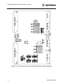
shipped with factory-installed jumpers. Figure 2-1 shows the EVB connector, switch, and jumper
header locations. The EVB consists of:
•
Dip switch DS1 lets you disconnect the on-board chip selects so you can use them on
the target board.
•
Dip switches DS2 through DS5 define the data bus reset configuration word.
•
Dip switch DS6 sets P2 ,P3 ,P4 and for BDM connector as DTE or DCE.
•
Jumper headers J1 through J7 are for customizing EVB operation (described in Table
2-2 and paragraphs 2.2.1 through 2.2.5).
•
Connector P1 is a SCSI interface connector (not populated).
•
Connectors P2 and P3 let you connect RS-232C devices to the EVB for evaluation
purposes.
•
Connector P4 is the serial port for communicating with the EVB using a host
computer. You must supply your own cable for communication with the EVB.
•
Connector P5 is the debug mode port for communicating with the EVB in background
debug mode.
•
Expansion connectors P6 and P8 let you connect MPC505 MCU signals to a target
board.
•
Connector P7 is the EVB +5 Vdc power connector.
•
POD1 through POD7 are 20-pin logic analyzer connectors for use in evaluating
MPC505 MCU signals.
•
Switch SW1 lets you reset the MPC505 MCU.
•
Switch SW2 lets you reset the EVB.
MPC505EVBUM/D
2-1
HARDWARE PREPARATION AND INSTALLATION
Figure 2-1. EVB Connector, Switch, and Jumper Header Location Diagram
2-2
MPC505EVBUM/D
HARDWARE PREPARATION AND INSTALLATION
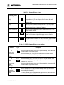
Table 2-1. Jumper Header Types
Jumper Header
Type
Symbol
Description
two-pin with solder
strap
Two-pin plate through holes (without jumper header block) and
designated as JX (X = the jumper header number). Bus wire
soldered between the two pins of the plate through holes to
create a short.
two-pin
Two-pin jumper header and designated as JX (X = the jumper
header number). Use a fabricated jumper to create a short
between the two pins of the jumper header.
two-pin with jumper
Two-pin jumper header with jumper, designated as JX (X = the
jumper header number).
three-pin
Three-pin jumper header, designated as JX (X = the jumper
header number). Use a fabricated jumper to create a short
between two of the three pins of the jumper header.
three-pin with jumper
Three-pin jumper header with jumper and designated as JX (X =
the jumper header number). To change the factory jumper header
configuration, move the jumper to the two desired pins.
Table 2-2. MPFB Jumper Header Descriptions
Jumper
Header
Type
J1
21
Crystal clock
sourcr select
header
(XTAL)
J2
Keep alive
power 2 select
header
MPC505EVBUM/D
Bus wire soldered between pins 1 and 2 (factory default); selects the EVB
on-board 4 MHz crystal clock source.
Bus wire between pins 1 and 2 is removed; lets you select an external
clock source as the MCU EXTAL input signal.
321
Clock
oscillator
source select
header
(EXTAL)
J3
Description
Bus wire between pins 1 and 2; lets you select an crystal oscillator clock
source as the MCU EXTAL input signal. (You must remove the bus wire
between pins 1 and 2 on
Bus wire soldered between pins 2 and 3 (factory default); selects the EVB
on-board 4 MHz crystal clock source.
321
Jumper installed on pins 1 and 2 (factory default); keep alive power 2 is
active as long as power is applied to the EVB (+3.3 Vdc present on the
VKAPWR2 pin of the MCU).
+3.3 Vdc external power supply attached to pins 2 and 3; maintains MCUinternal RAM after EVB power is turned OFF.
2-3
HARDWARE PREPARATION AND INSTALLATION
Table 2-2. MPFB Jumper Header Descriptions (continued)
Jumper
Header
Type
J4
321
Keep alive
power 1 select
header
System clock
selection
header
J7
System clock
selection
header
2-4
Jumper installed on pins 1 and 2 (factory default); MCU-internal oscillator,
time base, and decrementer operates as long as power is applied to the
EVB (+3.3 Vdc present on the VKAPWR2 pin of the MCU).
+3.3 Vdc external power supply attached to jumper header J4 pins 2 and 3;
maintains MCU-internal oscillator, time base, and decrementer operates
after EVB power is turned OFF.
J5
J6,
Description
Unused
3
2
1
Jumper installed on pins 1 and 2 (factory default); jumper headers J6 and
J7 select the MCU clock mode. The state of this signal during reset selects
the source of the system clock.
3
2
1
Jumper installed on pins 1 and 2 (factory default); jumper headers J6 and
J7 select the MCU clock mode.
MPC505EVBUM/D
HARDWARE PREPARATION AND INSTALLATION
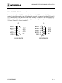
2.2.1
Crystal Clock Select Header (J1)
Jumper header J1 connects the crystal clock to the MCU XTAL pin clock source. The drawing
below shows the factory configuration: bus wire soldered on pins 1 and 2. This configuration
selects the crystal clock source; crystal in socket at located Y1. When you want to use the clock
oscillator as the EVB clock, remove the bus wire on J1 and move the bus wire on J2 from pins 2
and 3 to pins 1 and 2 (see paragraph 2.2.2). This disconnects the MCU XTAL pin from the
crystal clock circuit at location Y1 and selects the clock oscillator (U7) as the MCU clock source.
The frequency of the crystal clock circuit is 4 MHz. The frequency of the crystal oscillator circuit
can be as fast as 40 MHz.
Bus Wire
J1
2
1
The EVB comes with a 4 MHz crystal and a socket for a crystal oscillator. The EVB is factory
configured to use the 4 MHz crystal as the input. You can configure the clock frequency up to 33
MHz by setting the MF bits (bits 9-12) and RFD bits (bits 28-31) in register SCCR at address
0x8007_FC50 (shown in Table 2-3).
Table 2-3. MF and RFD Bits Required to Set Clock Speed
CLKOUT (megahertz)
RFD [0:3]
MF=
X000
(X4)
MF=
X001
(X5)
MF=
X010
(X6)
MF=
X011
(X7)
MF=
X100
(X8)
MF=
X101
(X9)
MF=
X110
(X10)
MF=
X111
(X11)
0 = 0000
16
20
24
28
32
NA
NA
NA
1 = 0001
8
10
12
14
16
18
20
22
2 = 0010
4
5
6
7
8
9
10
11
3 = 0011
2
2.5
32
3.5
4
4.5
5
5.5
4 = 0100
1
1.25
1.5
1.75
2
2.25
2.5
2.75
5 = 0101
.5
.625
.75
.875
1
1.125
1.25
1.375
6 = 0110
.25
.313
.375
.438
.5
.563
.625
.688
7 = 0111
.125
.156
.188
.219
.25
.281
.313
.344
MPC505EVBUM/D
2-5
HARDWARE PREPARATION AND INSTALLATION
2.2.2
Clock Source Select Header (J2)
Use jumper header J2 to select either a crystal or clock oscillator as the MCU clock source. The
drawing below shows the factory configuration: bus wire soldered on pins 2 and 3. This
configuration selects the crystal clock source; crystal in socket at located Y1. When you want to
use the clock oscillator as the EVB clock, move the bus wire on J2 from pins 2 and 3 to pins 1
and 2 and remove the bus wire on J1 (see paragraph 2.2.1). This disconnects the MCU XTAL pin
from the crystal clock circuit at location Y1 and selects the crystal oscillator (U7) as the MCU
clock source. The frequency of the crystal clock circuit is 4 MHz. The frequency of the crystal
oscillator circuit can be as fast as 40 MHz.
Bus Wire
J2
3
2.2.3
2
1
Keep Alive Power 2 Select Header (J3)
Jumper header J3 provides power to the MCU-internal RAM module via the MCU VKAPWR2
pin. You may use either the on-board +3.3 Vdc (jumper on J3 pins 1 and 2) or connect an
external +3.3 Vdc power supply to J3 pins 2 and 3. An external +3.3 Vdc power supply on J3
pins 2 and 3 will maintain MCU-internal RAM data after EVB power is turned OFF. To attach
an external power supply to VKAPWR2: remove the jumper on J3 pins 1 and 2, and connect the
power supply ground to J3 pin 3 and +3.3 Vdc to pin 2.
CAUTION
Applying power to the EVB with J4 removed and no external
power supply attached to J4 will damage the MPC505 MCU.
Always keep a jumper or an external +3.3 Vdc power supply on J4
pins 1 and 2. If using an external power supply, apply VKAPWR1
before powering up the EVB.
2-6
MPC505EVBUM/D
HARDWARE PREPARATION AND INSTALLATION
2.2.4
Keep Alive Power 2 Select Header (J4)
Jumper header J3 provides power to the MCU-internal oscillator, time base, and decementer
modules via the MCU VKAPWR1 pin. You may use either the on-board +3.3 Vdc (jumper on J4
pins 1 and 2) or connect an external +3.3 Vdc power supply to J4 pins 2 and 3. An external +3.3
Vdc power supply on J4 pins 2 and 3 will maintain MCU-internal RAM data after EVB power is
turned OFF. To attach an external power supply to VKAPWR1: remove the jumper on J4 pins 1
and 2, and connect the power supply ground to J4 pin 3 and +3.3 Vdc to pin 2.
CAUTION
Applying power to the EVB with J4 removed and no external
power supply attached to J4 will damage the MPC505 MCU.
Always keep a jumper or an external +3.3 Vdc power supply on J4
pins 1 and 2. If using an external power supply, apply VKAPWR1
before powering up the EVB.
2.2.5
Burst Memory Select Header (J5)
Unused.
MPC505EVBUM/D
2-7
HARDWARE PREPARATION AND INSTALLATION
2.2.6
System Clock Selection Headers (J6 and J7)
Jumper headers J6 and J7 let you define the system clock source. The factory configuration
(shown below) is for normal operation; a fabricated jumper on J6 and J7 pins 1 and 2. Refer to
Table 2-4 for configuring the system clock source.
Table 2-4. System Clock Source Configuration
MODCLK (J6)
Jumper Settings
VDDSYN (J7)
Jumper Settings
System Phase-LockLoop Options
1 and 2 (default)
1 and 2 (default)
2 and 3
1 and 2
1:1 Mode
1 and 2
2 and 3
SPLL Bypass Mode
2 and 3
2 and 3
Special Test Mode
Normal Operation
J6
3
2
1
Fabricated Jumpers
J7
3
2
1
2-8
MPC505EVBUM/D
HARDWARE PREPARATION AND INSTALLATION
2.2.7
EVB LED Descriptions
There are three LEDs on the EVB. Their functions are:
2.2.8
•
LD1 – 3.3 Vdc power: ON = 3.3 Vdc power is applied to the EVB.
•
LD2 – Debug Mode: ON = MPC505 is in debug mode
•
LD3 – +5 Vdc power: ON = power is applied to the EVB.
Optional Memory Configuration
There are eight 52-pin PLCC sockets on the EVB (U19, U20, U21, U22, U29, U30, U31, and
U32) for synchronous static RAM (SSRAM) devices. These sockets are paired as upper and
lower words and organized for long-word (32 bits wide) data transfers. Each pair is refered to as
BANKx. Table 2-5 shows on-board, memory configuration options.
Table 2-5. Optional Memory Configuration
Bank
Upper Word
Lower Word
64Kb Memory
Part Numbers
128Kb Memory
Part Numbers
BANK1
U29
U19
MCM67M518
MCM67M618
BANK2
U30
U20
MCM67M518
MCM67M618
BANK3
U31
U21
MCM67M518
MCM67M618
BANK4
U32
U22
MCM67M518
MCM67M618
The SSRAM factory default for the EVB is 128 kilobytes (two 64Kb I.C.s) installed in BANK1
(U19 and U29). You may increase the amount of on-board SSRAM to 256 kilobytes by
increasing the memory in sockets U19 and U29. You can further expand on-board memory by
populating U20, U21, U22, U30, U31, and U32 with additional SSRAM devices in each bank.
The EVB can have up to 1 megabyte of on-board SSRAM.
MPC505EVBUM/D
2-9
HARDWARE PREPARATION AND INSTALLATION
2.2.9
EVB Reset Switches
There are two reset switches on the EVB:
•
Switch SW1 lets you reset the MPC505 MCU
•
Switch SW2 lets you reset the EVB.
2.2.10 EVB DIP Switches
There are six DIP switches on the EVB (DS1 – DS6):
2-10
•
DS1 – Attaches the MCU chip selects to the EVB on-board memory and peripheral
devices. You may disable on-board chip selects and connect them via the expansion
connectors (P6 and P8) to external memory or peripheral devices.
•
DS2, DS3, DS4, DS5 – Data Bus Reset Configuration Word
•
DS6 – On the EVB are 3 RS232 ports (P2, P3, & P4) and one background debug
mode connector (P5). Each of the RS-232 ports can be either DTE or DCE port
(defined by DS6 switches 2, 3 and 4). While the host computer may be connected to
the RS-232 port or the debug mode connector (DS6 switch 1).
MPC505EVBUM/D
HARDWARE PREPARATION AND INSTALLATION
2.2.10.1
Chip Select Dip Switch (DS1)
The MPC505 MCU uses several chip selects on-board to control EVB functionality (memory and
peripheral devices). You can redefine these chip selects to control external devices via the
expansion connectors. To avoid conflicts between on-board and external devices, disable the
appropriate chip select by setting the appropriate DS1 switch (see Table 2-6).
Table 2-6. Chip Select Dip Switch (DS1)
Pin
Chip Select
1
CSBOOT
2
FOE
Flash output enable (U24, U25, U27, U28)
3
CS1
Burst RAM Bank1 (U19, U29)
4
CS2
Burst RAM Bank2 (U20, U30)
5
CS3
Burst RAM Bank3 (U21, U31)
6
CS4
Burst RAM Bank4 (U22, U32)
7
CS5
SCSI DUART (U4)
8
—
MPC505EVBUM/D
Device Connected to Chip Select
Flash chip select (U24, U25, U27, U28)
UNUSED
2-11
HARDWARE PREPARATION AND INSTALLATION
2.3.10.2
Reset Data Dip Switches (DS2 – DS5)
Dip switches DS2 – DS5 are connected through 4 buffers on the MPC505 MCU data bus (D31 –
D0). At RESET the MCU reads the data bus and changes its configuration according to these
switches ("ON" = 0 LOGIC).
There are two reset configuration modes: data bus configuration mode (pertinent to the EVB) or
internal default mode. In either mode the configuration is set by the MCU driving a configuration
word onto the internal data bus. Table 2-7 describes the configuration options. The EVB Default
Mode column shows the default reset configuration word. The default reset data bus
configuration word is X9E5EF4A3. For information on the internal reset configuration mode
refer to the PowerPC MPC505 RISC Microcontroller Technical Summary, MPC505TS/D.
Table 2-7. Data Bus Reset Configuration Word
Data
Bus
Bit
Configuration
Function
Effected
0
Address Bus
1
Effect of
Mode Select = 1
During Reset
Effect of
Mode Select = 0
During Reset
EVB
Default
Mode
Minimum Bus Mode
ADDR[0:11] = CS[0:11]
Maximum Bus Mode
ADDR[0:11] = Address Pins
1
Vector Table Location
(IP Bit)
Vector Table
0xFFF0 0000
Vector Table
0x0000 0000
0
2
Burst Type/Indication
Type 2/LAST
Type 1/BDIP
0
3
Interface Type for
CSBOOT
ITYPE = 001
Asynchronous (Time to
Hi-Z = 2Clk)
ITYPE = 1000
Synchronous Burst
1
4
CSBOOT Port Size
32-Bit
16-Bit
1
5
Reset Configuration
Source For DATA[6:13]
Latch Configuration from
external pins.
Latch Configuration from
internal defaults.
1
[6:8]
TA Delay For CSBOOT
TA Delay Encoding
000
001
010
011
100
101
110
111
# of Wait States
0
1
2
3
4
5
6
7
2-12
100
MPC505EVBUM/D
HARDWARE PREPARATION AND INSTALLATION
Table 2-7. Data Bus Reset Configuration Word (continued)
Data
Bus
Bit
Configuration
Function
Effected
[9:10]
IMEMBASE[0:1]
IMEMBASE
00
01
10
11
Block Placement
Start Addr: 0x0000 0000
End Addr: 0x000F FFFF
Start Addr: 0xFFF0 0000
End Addr: 0xFFFF FFFF
10
[11:12]
LMEMBASE[0:1]
LMEMBASE
00
01
10
11
SRAM Block Placement
Start address: 0x0000 0000
End address: 0x000F FFFF
Start address: 0xFFF0 0000
End address: 0xFFFF FFFF
11
13
Effect of
Mode Select = 1
During Reset
Reset configuration
Latch configuration from
source for DATA[14:21] external pins
Effect of
Mode Select = 0
During Reset
EVB
Default
Mode
Latch configuration from
internal defaults.
1
CT[0:3], AT[0:1], TS
PJ[1:7]
1
WR, BDIP
PK[0:1]
0
14
CT[0:3], AT[0:1], TS
15
WR, BDIP
16
PLLL/DSDO, VF[0:2],
VFLS[0:1], WP[1:5]
DSDO, Pipe Tracking,
Watchpoints
PK[2:7], PL[2:7]
1
17
BURST, TEA, AACK,
TA, BE[0:3]
Handshake Pins
PORTI[0:7]
1
18
CR, BI, BR, BB, BG,
ARETRY
Bus Arbitration Pins
PM[2:7]
1
19
Release reset when PLL Release reset when PLL Hold reset 16 clocks after reset
locked
locked and after 16 clocks negated.
(when not in PLL 1:1
mode)
20
21
Reserved
Reset Configuration
Latch Configuration from
Source For DATA[22:31] external pins.
22
23
MPC505EVBUM/D
0
Latch Configuration from
internal defaults.
Reserved
IEN
I-bus Memory modules
are enabled.
1
1
0
I-bus Memory modules are
disabled and emulated
externally.
0
2-13
HARDWARE PREPARATION AND INSTALLATION
Table 2-7. Data Bus Reset Configuration Word (continued)
Data
Bus
Bit
Configuration
Function
Effected
24
LEN
25
PRUMODE
26
ADDR[12:15]
Effect of
Mode Select = 1
During Reset
Effect of
Mode Select = 0
During Reset
EVB
Default
Mode
L-bus Memory modules
are enabled.
L-bus Memory modules are
disabled and emulated
externally.
1
Forces accesses to Ports
A, B, I, J, K, and L to go
external.
No effect
0
ADDR[12:15]
PB[4:7]
1
27
Reserved
0
28
Reserved
0
29
Reserved
0
30
Test Slave Mode Enable Test Slave Mode
Disabled
Test Slave Mode Enabled
1
31
Test Transparent Mode Test Transparent Mode
Enable
Disabled
Test Transparent Mode
Enabled
1
2-14
MPC505EVBUM/D
HARDWARE PREPARATION AND INSTALLATION
2.2.10.3
DTE/DCE Settings
DS6 switch 1 lets you define which connector to use with your host computer. While DS6
switches 2 - 4 lets you define I/O connectors P2, P3, and P4 as DTE or DCE. Table 2-8 shows
DS6 switch settings.
Table 2-8. DS6 Communication Type Switch Settings
Pin #
Signal Name
Connector
1
OEDSDIDSCK
P4/P5
Description
Switch to ON when using P4 as the I/O port
Switch to OFF when using BDM connector P5 as the
I/O port
2
ADCE_DTE~
P2
ON = DTE
OFF = DCE
3
BDCE_DTE~
P3
ON = DTE
OFF = DCE
4
CDCE_DTE~
P4
ON = DTE
OFF = DCE
5
—
UNUSED
6
—
UNUSED
7
—
UNUSED
8
—
UNUSED
MPC505EVBUM/D
2-15
HARDWARE PREPARATION AND INSTALLATION
2.3 INSTALLATION INSTRUCTIONS
The EVB is designed for table top operation. A user supplied power supply and host computer
(with an RS-232C port) are required for EVB operation.
2.3.1
Host Computer – EVB Interconnection
Interconnection of a host computer to the EVB is accomplished via a user supplied 25-pin flat
cable assembly. One end of the cable assembly is connected to the EVB connector P4 (shown
below). The other end of the cable assembly is connected to the host computer. For connector pin
assignments and signal descriptions of the EVB I/O port connector P4, refer to Appendix B.
P4
NC
CTXD
CRXD
CRTS
CCTS
CDSR
GND
CDCD
NC
NC
NC
NC
NC
1
2
3
4
5
6
7
8
9
10
11
12
13
14
15
16
17
18
19
20
21
22
23
24
25
NC
NC
NC
NC
NC
NC
CDTR
NC
NC
NC
NC
NC
HOST COMPUTER
2-16
MPC505EVBUM/D
HARDWARE PREPARATION AND INSTALLATION
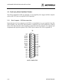
2.3.2
Background Mode Connector (P5)
Use connector P5 (pinouts shown below) to communicate with the EVB via the background
debug mode (BDM). You may use the serial development interface (SDI) as your BDM interface.
Connect one end of the SDI to your host computer and the other to connector P5. For more
information about the SDI refer to the M68SDIUM Users Manual, M68SDIUM/D.
P5
MPC505EVBUM/D
VFLS0
1
•
•
2
SRESET~
GND
3
•
•
4
DSCK
GND
5
•
•
6
VFLS1
RESET~
7
•
•
8
DSDI
VCC/V3.3
9
•
•
10 DSDO
2-17
HARDWARE PREPARATION AND INSTALLATION
2.3.3
Power Supply – EVB Interconnection
The EVB requires +5 Vdc @ 2 amp power supply for operation. Connector P7 pin 1 is +5 Vdc;
pins 2 and 3 are ground (shown in Figure 2-2). Use 16-22 AWG wire in the connector (supplied
with the board). EVB power supply interconnection for connector P7 is shown below.
Figure 2-2. Power Supply Connector (P7)
2-18
MPC505EVBUM/D
HARDWARE PREPARATION AND INSTALLATION
2.3.4
RS-232C – EVB Interconnection
Interconnection of an RS-232C compatible device to the EVB is accomplished via a user
supplied 9-pin cable assembly. One end of the cable assembly is connected to either EVB port P2
or P3 (shown below). The other end of the cable assembly is connected to the user supplied RS232C compatible device. For connector pin assignments and signal descriptions of the EVB RS232C ports P2 and P3, refer to Appendix B.
P2
ADCD
ARXD
ATXD
ADTR
GND
1
2
3
4
5
P3
6
7
8
9
ADSR
ARTS
ACTS
NC
RS-232 DEVICE
MPC505EVBUM/D
BDCD
BRXD
BTXD
BDTR
GND
1
2
3
4
5
6
7
8
9
BDSR
BRTS
BCTS
NC
RS-232 DEVICE
2-19
HARDWARE PREPARATION AND INSTALLATION
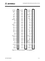
2.3.5
EVB Expansion Connectors
There are two expansion connectors (P6 and P8) on the EVB. The pin assignments for the
expansion connectors are in Figures 2-3 and 2-4. Signal descriptions are in Appendix B.
C
B
A
BSWE3~
1
•
VCC
1
•
FOE~
1
•
BSWE1~
2
•
VCC
2
•
CS5~
2
•
CSBT~
3
•
VCC
3
•
A10
3
•
A21
4
•
BSWE2~
3
•
A11
4
•
A22
5
•
BSWE0~
4
•
A12
5
•
A23
6
•
CS4~
6
•
A13
6
•
A24
7
•
CS3~
7
•
A14
7
•
A25
8
•
CS2~
8
•
A15
8
•
A26
9
•
CS1~
9
•
A16
9
•
A27 10
•
GND 10
•
A17 10
•
A28 11
•
GND 11
•
A18 11
•
A29 12
•
GND 12
•
A19 12
•
GND 13
•
GND 13
•
A20 13
•
D16 14
•
GND 14
•
GND 14
•
D17 15
•
GND 15
•
D0 15
•
D18 16
•
GND 16
•
D1 16
•
D19 17
•
GND 17
•
D2 17
•
D20 18
•
GND 18
•
D3 18
•
D21 19
•
GND 19
•
D4 19
•
D22 20
•
GND 20
•
D5 20
•
D23 21
•
GND 21
•
D6 21
•
D24 22
•
GND 22
•
D7 22
•
D25 23
•
GND 23
•
D8 23
•
D26 24
•
GND 24
•
D9 24
•
D27 25
•
GND 25
•
D10 25
•
D28 26
•
GND 26
•
D11 26
•
D29 27
•
GND 27
•
D12 27
•
D30 28
•
GND 28
•
D13 28
•
D31 29
•
GND 29
•
D14 29
•
GND 30
•
CLKOUT 30
•
D15 30
•
NC 31
•
GND 31
•
GND 31
•
NC 32
•
GND 32
•
NC 32
•
Figure 2-3. Expansion Connector P6 Pin Assignments
2-20
MPC505EVBUM/D
HARDWARE PREPARATION AND INSTALLATION
C
B
A
+3.3 Vdc
1
•
+3.3 Vdc
1
•
+3.3 Vdc
1
•
+3.3 Vdc
2
•
+3.3 Vdc
2
•
+3.3 Vdc
2
•
BDIP~
3
•
GND
3
•
AACK~
3
•
BI~
4
•
GND
3
•
TS~
4
•
IRQ3~
5
•
GND
4
•
VDDSYN
5
•
IRQ2~
6
•
GND
6
•
IRQ6~
6
•
IRQ1~
7
•
GND
7
•
IRQ5~
7
•
IRQ0~
8
•
GND
8
•
IRQ4~
8
•
MODCLK
9
•
GND
9
•
CT0
9
•
NC 10
•
GND 10
•
CT1 10
•
NC 11
•
GND 11
•
CT2 11
•
GND 12
•
GND 12
•
CT3 12
•
BURST~ 13
•
GND 13
•
GND 13
•
WP0~ 14
•
GND 14
•
VF0 14
•
WP1~ 15
•
GND 15
•
VF1 15
•
WP2~ 16
•
GND 16
•
VF2 16
•
WP3~ 17
•
GND 17
•
R_W~ 17
•
WP4~ 18
•
GND 18
•
TA~ 18
•
WP5~ 19
•
GND 19
•
TEA~ 19
•
NC 20
•
GND 20
•
AT1 20
•
AT0 21
•
GND 21
•
NC 21
•
ECROUT 22
•
GND 22
•
ARETRY 22
•
BE0~ 23
•
GND 23
•
BG~ 23
•
BE1~ 24
•
GND 24
•
BR~ 24
•
BE2~ 25
•
GND 25
•
BB~ 25
•
BE3~ 26
•
GND 26
•
RESET~ 26
•
NC 27
•
GND 27
•
SRESET~ 27
•
CR~ 28
•
GND 28
•
VFLS1 28
•
PDWU 29
•
GND 29
•
VFLS0 29
•
NC 30
•
VCC 30
•
DSDI 30
•
GND 31
•
VCC 31
•
DSCK 31
•
GND 32
•
VCC 32
•
DSDO 32
•
Figure 2-4. Expansion Connector P7 Pin Assignments
MPC505EVBUM/D
2-21
HARDWARE PREPARATION AND INSTALLATION
2.3.6
Logic Analyzer Connectors
Use connectors POD1 through POD7 to connect a logic analyzer to the circuit being evaluated.
Below are the pin assignments for the logic analyzer connectors.
POD1
POD2
NC
1
•
•
2
NC
NC
1
•
•
2
NC
TS~
3
•
•
4
FOE~
NC
3
•
•
4
A16
CS1~
5
•
•
6
CS2~
A17
5
•
•
6
A18
CS3~
7
•
•
8
CS4~
A19
7
•
•
8
A20
CS5~
9
•
•
10 BSWE0~
A21
9
•
•
10 A22
BSWE1~ 11
•
•
12 BSWE2~
A23 11
•
•
12 A24
BSWE3~ 13
•
•
14 A10
A25 13
•
•
14 A26
A11 15
•
•
16 A12
A27 15
•
•
16 A28
A13 17
•
•
18 A14
A29 17
•
•
18 GND (A30)
A15 19
•
•
20 GND
(A31) GND 19
•
•
20 GND
POD3
2-22
POD4
NC
1
•
•
2
NC
NC
1
•
•
2
NC
NC
3
•
•
4
D16
NC
3
•
•
4
D0
D17
5
•
•
6
D18
D1
5
•
•
6
D2
D19
7
•
•
8
D20
D3
7
•
•
8
D4
D21
9
•
•
10 D22
D5
9
•
•
10 D6
D23 11
•
•
12 D24
D7 11
•
•
12 D8
D25 13
•
•
14 D26
D9 13
•
•
14 D10
D27 15
•
•
16 D28
D11 15
•
•
16 D12
D29 17
•
•
18 D30
D13 17
•
•
18 D14
D31 19
•
•
20 GND
D15 19
•
•
20 GND
MPC505EVBUM/D
HARDWARE PREPARATION AND INSTALLATION
POD5
POD6
NC
1
•
•
2
NC
NC
1
•
•
2
NC
NC
3
•
•
4
DSCK
NC
3
•
•
4
CLKOUT
DSDI
5
•
•
6
DSDO
RESET~
5
•
•
6
SRESET~
VF0
7
•
•
8
VF1
CT0
7
•
•
8
CT1
VF2
9
•
•
10 VFLS0
CT2
9
•
•
10 CT3
VFLS1 11
•
•
12 WP0~
CR~ 11
•
•
12 BR~
WP1~ 13
•
•
14 WP2~
BB~ 13
•
•
14 BG~
WP3~ 15
•
•
16 WP4~
IRQ0~ 15
•
•
16 IRQ1~
WP5~ 17
•
•
18 NC
ECROUT 17
•
•
18 MODCLK
NC 19
•
•
20 GND
PDWU 19
•
•
20 GND
POD7
2.3.7
NC
1
•
•
2
NC
CLKOUT
3
•
•
4
BURST~
TEA~
5
•
•
6
AACK~
TA~
7
•
•
8
BE0~
BE1~
9
•
•
10 BE2~
BE3~ 11
•
•
12 BDIP~
R_W~ 13
•
•
14 TS~
AT0 15
•
•
16 AT1~
BI~ 17
•
•
18 ARETRY~
CSBT~ 19
•
•
20 GND
SCSI
The EVB printed circuit board includes an optional SCSI port. The required parts for the SCSI
port are user supplied. SCSI port parts list is provided in Table 2-9.
Table 2-9. SCSI Port Parts List
Reference Designation
P1
U1, U2
U3
MPC505EVBUM/D
Component Description
SCSI Connector, AMP 749830-5
I.C., DS2107S, SCSI Terminator, DALLAS
Semiconductor
I.C., 53C90B, SCSI Controller, NCR
2-23
HARDWARE PREPARATION AND INSTALLATION
2-24
MPC505EVBUM/D
FUNCTIONAL DESCRIPTION
CHAPTER 3
FUNCTIONAL DESCRIPTION
3.1
INTRODUCTION
This chapter is a functional description of the EVB and its components.
3.2
EVB DESCRIPTION
The EVB may be configured in either of two ways; the BCC mounted on the PFB or the BCC
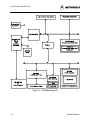
mounted on the target system. Figure 3-1 is the EVB block diagram.
When the BCC is mounted on the PFB, you may evaluate the MCU and debug user developed
code. To do this connect a terminal or host computer to PFB connector P9 and run the MPCbug
debug monitor program. Logic analyzer connection may be made to connectors P1 through P6 of
the PFB.
Mount the BCC on the target system to verify hardware design. With the BCC mounted on the
target system, MC68332 MCU device emulation with hardware breakpoints is possible by
connecting a PC to BCC connector P4 and running MPCbug debug monitor. Logic analyzer
connection may be made to connectors P1 and P2 of the BCC.
MPC505EVBUM/D
3-1
FUNCTIONAL DESCRIPTION
Figure 3-1. EVB Block Diagram
3-2
MPC505EVBUM/D
FUNCTIONAL DESCRIPTION
3.3
MCU SUMMARY
The resident MC68332 Microcontroller Unit (MCU) of the BCC provides resources for
designing, debugging, and evaluating MC68332 MCU based target systems and simplifies user
evaluation of prototype hardware/software products.
The MCU device is a 32-bit integrated microcontroller, combining high-performance data
manipulation capabilities with powerful peripheral subsystems. The MCU includes:
•
32-bit central processor unit (CPU32)
•
Time processor unit (TPU)
•
Queued serial module (QSM)
•
Random access memory (RAM)
•
External bus interface
•
Chip selects
•
System clock
•
Test module
3.3.1
32-Bit Central Processor Unit
The CPU32 is the central processor for the MC68332 MCU device. The CPU32 is source and
object code compatible with the MC68000 and MC68010. All user programs can be executed
unchanged. The CPU32 features are:
•
32-Bit internal data path and arithmetic hardware - 16-bit external data bus
•
32-Bit internal address bus - 24-bit external address bus
•
Powerful instruction set
•
Eight 32-bit general purpose data registers
•
Seven 32-bit general purpose address registers
•
Separate user and supervisor stack pointers and address spaces
•
Separate program and data address spaces
•
Flexible addressing modes
•
Full interrupt processing
MPC505EVBUM/D
3-3
FUNCTIONAL DESCRIPTION
3.3.2
Time Processor Unit
The Time Processor Unit (TPU) optimizes performance of time-related activities. The TPU has a
dedicated execution unit, tri-level prioritized scheduler, data storage RAM, dual time bases, and
microcode ROM which drastically reduces the need for CPU intervention. The TPU controls
sixteen independent, orthogonal channels; each channel has an associated I/O pin and can
perform any time function. Each channel also contains a dedicated event register, for both match
and input capture functions.
Each channel can be synchronized to either of two 16-bit, free-running counters with a pre-scaler.
One counter, based on the system clock, provides resolution of TPU system clock divided by 4.
The second counter, based on an external reference, also provides resolution of TPU system
clock divided by 8. Channels may also be linked together, allowing the user to reference
operations on one channel to the occurrence of a specified action on another channel, providing
inter-task control.
3.3.3
Queued Serial Module
The QSM contains two serial ports. The queued serial peripheral interface (QSPI) port provides
easy peripheral expansion or inter-processor communications via a full-duplex, synchronous,
three-line bus: data-in, data-out, and a serial clock. Four programmable peripheral select pins
provide address-ability for as many as 16 peripheral devices. A QSPI enhancement is an added
queue in a small RAM. This lets the QSPI handle as many as 16 serial transfers of 8- to 16-bits
each, or to transmit a stream of data as long as 256 bits without CPU intervention. A special
wrap-around mode lets the user continuously sample a serial peripheral, automatically updating
the QSPI RAM for efficient interfacing to serial peripheral devices (such as analog-to-digital
converters).
The serial communications interface (SCI) port provides a standard non-return to zero (NRZ)
mark/space format. Advanced error detection circuitry catches noise glitches to 1/16 of a bit time
in duration. Word length is software selectable between 8- or 9-bits, and the SCI modulus-type,
baud rate generator provides baud rates from 64 to 524k baud, based on a 16.77 MHz system
clock. The SCI features full- or half-duplex operation, with separate transmitter and receiver
enable bits and double buffering of data. Optional parity generation and detection provide either
even or odd parity check capability. Wake-up functions let the CPU run uninterrupted until either
a true idle line is detected or a new address byte is received.
3.3.4
Random Access Memory
2k bytes of static RAM are contained within the MC68332 MCU device. The RAM is used for
storage of variable and temporary data. RAM data size may be 8-bits (byte), 16-bits (word), or
32-bits (longword). The RAM can be mapped to any 2k byte boundary in the address map.
3-4
MPC505EVBUM/D
FUNCTIONAL DESCRIPTION
3.3.5
External Bus Interface
The external bus consists of 24 address lines and a 16-bit data bus. The data bus allows dynamic
sizing between 8- and 16-bit data accesses. A read-modify-write cycle (RMC) signal prevents
bus cycle interruption. External bus arbitration is accomplished by a three-line handshaking
interface.
3.3.6
Chip Selects
Twelve independently programmable chip selects provide fast, two-cycle external memory, or
peripheral access. Block size is programmable from 2 kilobytes through 1 megabyte. Accesses
can be selected for either 8- or 16-bit transfers. As many as 13 wait states can be programmed for
insertion during the access. All bus interface signals are automatically handled by the chip select
logic.
3.3.7
System Clock
An on-chip phase locked loop circuit generates the system clock signal to run the device up to
16.78 MHz from a 32.768 kHz watch crystal. The system speed can be changed dynamically,
providing either high performance or low power consumption under software control. The
system clock is a fully-static CMOS design, so it is possible to completely stop the system clock
via a low power stop instruction, while still retaining the contents of the registers and on-board
RAM.
3.3.8
Test Module
The test module consolidates the microcontroller test logic into a single block to facilitate
production testing, user self-test, and system diagnostics. Scan paths throughout the MC68332
provide signature analysis checks on internal logic. User self-test is initiated by asserting the test
pin to enter test mode. This test provides a pass/fail response to various externally supplied test
vectors.
3.4
USER MEMORY
On board the BCC is 32k x 16 bits of RAM and 64k x 16 bits of EPROM. The RAM is the
debug monitor storage area and user accessible memory space; the M68MPCBUG Debug
Monitor is stored in the BCC EPROMs. For debug monitor functionality see the M68MPCBUG
Debug Monitor User’s Manual, M68MPCBUG /AD1. Figure 3-3 is the EVB memory map.
The PFB has sockets for 32k x 16 or 64k x 16 bit RAM or 64k x 16 bit EPROM. The RAM
and/or EPROM, supplied by the user, is user-accessible memory space.
MPC505EVBUM/D
3-5
FUNCTIONAL DESCRIPTION
XXX7FF
INTERNAL RAM
(2)
(1 )
XXX000
FFFFFF
MCU
INTERNAL
MODULES
FFF000
OPTIONAL FPCP (3)
PFB: U5
FFE800
800000
ALTERNATE MCU
INTERNAL MODULES
LOCATION (4)
7FF000
OPTIONAL RAM/EPROM
PFB: U2 & U4
CPU32BUG EPROM
BCC: U1 & U2
110000 /120000 (5)
100000
0E0000
OPTIONAL RAM
PFB: U1 & U3
TARGET RAM
BCC: U3 & U4
SYSTEM RAM
BCC: U3 & U4
1.
2.
3.
4.
5.
020000
010000
003000
000000
CPU32BUG
INTERNAL STACK
CPU32BUG
INTERNAL
VARIABLES
CPU32BUG VECTOR
TABLE
TARGET VECTOR
TABLE
Consult the MCU device user’s manual.
XXbase address is user programmable. Internal modules, such as
internal RAM, can be configured on power-up/reset by using the
initilization table (INITTBL) covered in Appendix C of the
M68MPCBUG Debug Monitor User’s Manual, M68MPCBUG /AD1.
Floating point coprocessor - MC68881/MC68882.
See Appendix C of the M68MPCBUG Debug Monitor User’s Manual,
M68MPCBUG /AD1.
Depends on the memory device type used.
Figure 3-2. EVB Memory Map
3-6
MPC505EVBUM/D
FUNCTIONAL DESCRIPTION
3.5
I/O CONNECTORS
There are two 64-pin expansion connectors on the BCC (P1 and P2). Through these connectors
the BCC communicates with the PFB or target system. Background mode operation is available
through P3 and serial communication through P4. Chapter 5 contains a description of the
interface connectors pin assignments.
3.5.1
64-Pin Expansion Connectors
The expansion connectors interconnect the BCC to the PFB or target system. The pin-outs of the
MC68332 MCU device, serial communication, and background mode interface are available on
the expansion connectors.
3.5.2
Serial Communication Connectors
A terminal or host computer with terminal emulation (PCKERMIT.EXE, PROCOMM, etc.), can
be connected to the BCC or to the PFB. Terminal connections are provided through the serial
communication connectors, BCC P4 or to PFB P9.
3.5.3
Background Mode Interface Connector
The background debug mode is implemented in MCU microcode. In background mode, registers
can be viewed or altered, memory can be read or written, and test features can be executed.
Background mode is initiated by one of several sources: externally generated breakpoints,
internal peripherally generated breakpoints, software, and catastrophic exception conditions.
Instruction execution is suspended for the duration of background mode. Background mode
communications between the BCC and the development system are via a serial link (P3).
3.6
PFB DESCRIPTION
The PFB is the physical location for installing the BCC. The user may expand the user accessible
memory. I/O connectors are available for communication, power, and a logic analyzer.
3.6.1
Floating-Point Coprocessor Socket (U5)
Socket U5 on the PFB accommodates an optional coprocessor for the EVB. Either an MC68881
or an MC68882 coprocessor can be used in socket U5. The coprocessor software interface is not
part of the EVB, so must be provided by the user. For developing the coprocessor software
interface, see the application note MC68881 Floating-Point Coprocessor as a Peripheral in an
M68000 System, AN947.
MPC505EVBUM/D
3-7
FUNCTIONAL DESCRIPTION
The coprocessor interface is a transparent, logical extension of the MC68332 MCU device
registers and instructions. To the external environment the CPU and coprocessor execution
model appear to be on the same chip.
A coprocessor interface is an execution model based on sequential instruction execution by the
CPU and coprocessor. For optimum performance, the coprocessor interface lets floating point
instructions execute concurrently with CPU integer instructions. Concurrent instruction
execution is further extended by the coprocessor, which executes multiple floating-point
instructions simultaneously.
3.6.2
Logic Analyzer Connectors
To debug hardware and software developed for the MC68331 MCU device, connect a logic
analyzer to the desired pins of PFB connectors P1 - P6.
3-8
MPC505EVBUM/D
SUPPORT INFORMATION
CHAPTER 4
SUPPORT INFORMATION
4.1 INTRODUCTION
The tables in this chapter describe EVB connector signals.
4.2 CONNECTOR SIGNAL DESCRIPTIONS
The following are all the connectors on the board include pin number mnemonic and signal
description.
Connector P7 connects external power to the EVB. the host computer connects to the EVB via
P4. POD1 through POD7 let you connect a logic analyzer to the EVB. P2 and P3 are EVB I/O
ports for evaluating RS-232C devices.
NOTE
The signal descriptions in the following tables are for quick
reference only. For a complete description of the MCU signals
consult the appropriate MCU user’s manual, data book, or technical
summary. For a complete description of the SCSI signals consult
the appropriate NCR 53C90B User Manual Data Book. For a
complete description of the P2,P3 signals consult the appropriate
MOTOROLA M68681 User Manual Data Book.
Tables 4-1 through 4-19 list pin assignments for these connectors:
Table 4-1
SCSI connector P1 (not populated)
Table 4-9
Logic analyzer connector POD1
Table 4-2
RS-232C I/O port P2
Table 4-10
Logic analyzer connector POD2
Table 4-3
RS-232C I/O port P3
Table 4-11
Logic analyzer connector POD3
Table 4-4
Host computer connector P4
Table 4-12
Logic analyzer connector POD4
Table 4-5
Debug mode connector P5
Table 4-13
Logic analyzer connector POD5
Table 4-6
Expansion connector P6
Table 4-14
Logic analyzer connector POD6
Table 4-7
Input power connector P7
Table 4-15
Logic analyzer connector POD7
Table 4-8
Expansion connector P8
MPC505EVBUM/D
4-1
SUPPORT INFORMATION
Table 4-1. SCSI Connector (not populated)
4-2
Pin
Mnemonic
Signal
1
GND
GROUND
2
SDB0
SCSI DATA BUS (bit 0) – Bit 0 of the SCSI bi-directional data bus lines.
3
GND
GROUND
4
SDB1
SCSI DATA BUS (bit 1) – Bit 1 of the SCSI bi-directional data bus lines.
5
GND
GROUND
6
SDB2
SCSI DATA BUS (bit 2) – Bit 2 of the SCSI bi-directional data bus lines.
7
GND
GROUND
8
SDB3
SCSI DATA BUS (bit 3) – Bit 3 of the SCSI bi-directional data bus lines.
9
GND
GROUND
10
SDB4
SCSI DATA BUS (bit 4) – Bit 4 of the SCSI bi-directional data bus lines.
11
GND
GROUND
12
SDB5
SCSI DATA BUS (bit 5) – Bit 5 of the SCSI bi-directional data bus lines.
13
NC
14
SDB6
SCSI DATA BUS (bit 6) – Bit 6 of the SCSI bi-directional data bus lines.
15
GND
GROUND
16
SDB7
SCSI DATA BUS (bit 7) – Bit 7 of the SCSI bi-directional data bus lines.
17
GND
GROUND
18
SDBP
SCSI DATA BUS PARITY – SCSI bi-directional data parity line.
19 – 25
GND
GROUND
26
VCC
+5 VDC POWER – Input voltage (+5 Vdc @ 2.0 A) used by the EVB
logic circuits.
Not Connected
MPC505EVBUM/D
SUPPORT INFORMATION
Table 4-1. SCSI Connector (not populated) (continued)
Pin
Mnemonic
27 – 31
GND
GROUND
32
ATNI*
ATTENTION – Active-low output signal that indicates to the target that
the MPC505 has a message to send.
33 – 35
GND
GROUND
36
BSY
BUSY – Active low I/O signal that indicates the SCSI is busy.
37
GND
GROUND
38
ACK
ACKNOWLEDGE – Active-low handshake signal that indicates to the
target that the MPC505 has transfered a byte.
39
GND
GROUND
40
RST
RESET – Active-low output signal that indicates a reset condition. All
devices using the bus must release it.
41
GND
GROUND
42
MSG
MESSAGE – Active-low output signal that indicates the target is
sending a message.
43
GND
GROUND
44
SEL
SELECT – Active-low output signal used by the MPC505 to select a
target.
45
GND
GROUND
46
C/D
CONTROL/DATA – Active-low output signal that indicates whether
control of data is on the data bus. This signal is controlled by the target.
47
GND
GROUND
48
REQ
REQUEST – Active-low handshake signal that indicates to the MPC505
that the target has transfered a byte.
49
GND
GROUND
50
I/O
MPC505EVBUM/D
Signal
INPUT/OUTPUT – Active-low output signal driven by the target that
controls data direction.
4-3
SUPPORT INFORMATION
Table 4-2. RS-232C I/O Connector P2 Pin Assignments
Pin
Mnemonic
Signal
1
ADCD*
DATA CARRIER DETECT – An output signal used to indicate an
acceptable received line (carrier) signal has been detected.
2
ARXD
RECEIVE DATA – RS-232C serial input signal.
3
ATXD
TRANSMIT – RS-232C serial output signal.
4
ADTR*
DATA TERMINAL READY – An output line that indicates an on-line/inservice/active status.
5
GND
GROUND
6
ADSR*
DATA SET READY – An output signal (held high) that indicates an online/in-service/active status.
7
ARTS
REQUEST TO SEND – An input signal used to request permission to
transfer data.
8
ACTS*
CLEAR TO SEND – An output signal that indicates a ready-to-transfer
data status.
9
NC
Not Connected
4-4
MPC505EVBUM/D
SUPPORT INFORMATION
Table 4-3. RS-232C I/O Connector P3 Pin Assignments
Pin
Mnemonic
1
BDCD*
DATA CARRIER DETECT – An output signal used to indicate an
acceptable received line (carrier) signal has been detected.
2
BRXD
RECEIVE DATA – RS-232C serial input signal.
3
BTXD
TRANSMIT – RS-232C serial output signal.
4
BDTR*
DATA TERMINAL READY – An output line that indicates an on-line/inservice/active status.
5
GND
6
BDSR*
DATA SET READY – An output signal (held high) that indicates an online/in-service/active status.
7
BRTS
REQUEST TO SEND – An input signal used to request permission to
transfer data.
8
BCTS*
CLEAR TO SEND – An output signal that indicates a ready-to-transfer
data status.
9
NC
MPC505EVBUM/D
Signal
GROUND
Not Connected
4-5
SUPPORT INFORMATION
Table 4-4. Host Computer Connector P4 Pin Assignments
4-6
Pin
Mnemonic
Signal
1
NC
2
CTXD
TRANSMIT – RS-232C serial output signal.
3
CRXD
RECEIVE DATA – RS-232C serial input signal.
4
CRTS
REQUEST TO SEND – An input signal used to request permission to
transfer data.
5
CCTS*
CLEAR TO SEND – An output signal that indicates a ready-to-transfer
data status.
6
ADSR*
DATA SET READY – An output signal (held high) that indicates an online/in-service/active status.
7
GND
8
CDCD*
9 - 19
NC
20
ADTR*
21 - 25
NC
Not Connected
GROUND
DATA CARRIER DETECT – An output signal used to indicate an
acceptable received line (carrier) signal has been detected.
Not Connected
DATA TERMINAL READY – An output line that indicates an on-line/inservice/active status.
Not Connected
MPC505EVBUM/D
SUPPORT INFORMATION
Table 4-5. Debug Mode Connector P5 Pin Assignments
Pin
Mnemonic
1
VFLS0
2
SRESET*
3
GND
GROUND
4
DSCK
DEVELOPMENT SERIAL CLOCK – Serial input clock for background
debug mode.
5
GND
GROUND
6
VFLS1
7
RESET*
8
DSDI
DEVELOPMENT SERIAL DATA IN – Serial data input signal for debug
mode.
9
VCC
+5 VDC POWER – Input voltage (+5 Vdc @ 2.0 A) used by the EVB
logic circuits.
10
DSDO
DEVELOPMENT SERIAL DATA OUT – Serial data output signal for
debug mode.
MPC505EVBUM/D
Description
VISIBILITY FLUSH - If VFLS0 and VFLS1 are high the MPC505 is in
background debug mode.
SYSTEM RESET – Active-low, MPC505 MCU output signal that is
asserted by the MCU during reset.
VISIBILITY FLUSH - If VFLS0 and VFLS1 are high the MPC505 is in
background debug mode.
RESET – Active-low, input signal that resets the MPC505 MCU.
4-7
SUPPORT INFORMATION
Table 4-6. P6 Expansion Connector Pin Assignments
Pin
Mnemonic
A-1
FOE*
FLASH OUTPUT ENABLE - Active low output signal that lets you read
the EVB on-board flash memory.
A-2
CS5*
CHIP SELECT 5 Output signal that selects peripheral/memory devices
at programmed addresses.
A-3 A-13
A10 A20
A-14
GND
A-15 A-30
D0 D15
A-31
GND
A-32
NC
B-1 B-3
VCC
+5 VDC POWER –Input voltage (+5 Vdc @ 2.0 A) used by the EVB
logic circuits.
B-4
BSWE2*
Address signal A8 - one signal of the three-state output address bus.
B-5
BSWE0*
Address signal A6 - one signal of the three-state output address bus.
B-6 B-9
CS4* CS1*
CHIP SELECT (4 – 1) – Output signals that select peripheral/memory
devices at programmed addresses.
B-10 B-29
GND
B-30
CLKOUT
B-31, B-32
GND
C-1
BSWE3*
Address signal A9 - one signal of the three-state output address bus.
C-2
BSWE1*
Address signal A7 - one signal of the three-state output address bus.
C-3
CSBT*
BOOT CHIP SELECT – Active-low output signal that selects peripheral
or memory devices at programmed addresses.
C-4 C-12
A21 A29
ADDRESS BUS (bits 21 29) – 9-pins of the three-state output address
bus.
C-13
GND
C-14 C-29
D16 D31
C-30
GND
C-31, C-32
NC
4-8
Signal
ADDRESS BUS (bits 10 – 20) – 11-pins of the three-state output
address bus.
GROUND
DATA BUS (bits 0 15) – Bi-directional data pins.
GROUND
Not Connected
GROUND
SYSTEM CLOCK OUT – Output signal that is the MPC505 MCU
internal system clock.
GROUND
GROUND
DATA BUS (bits 16 31) – Bi-directional data pins.
GROUND
Not Connected
MPC505EVBUM/D
SUPPORT INFORMATION
Table 4-7. Input Power Connector P7 Pin Assignments
Pin
Mnemonic
Signal
1
VCC
+5 VDC POWER – Input voltage (+5 Vdc @ 2.0 A) used by the EVB
logic circuits. The "VCC" write on the board nere the coresponding pin.
2
GND
GROUND The "GND" write on the board nere the coresponding pin
3
GND
GROUND The "GND" write on the board nere the coresponding pin
Table 4-8. P8 Expansion Connector Pin Assignments
Pin
Mnemonic
A-1, A-2
V3.3
A-3
AACK*
A-4
TS*
A-5
VDDSYN
VDDSYN – Clock synthesizer power.
A-6 A-8
IRQ6* –
IRQ4*
INTERRUPT REQUEST (6 -4) – Prioritized active low input lines that
requests MCU synchronous interrupts. IRQ1* has the highest priority.
A-9 A-12
CT0 CT3
A-13
GND
A-14 A-16
VF0 VF2
VISIBILITY FETCH – Instruction queue status bits that indicate the last
fetched instruction or the number of instructions flushed from the
instruction queue.
A-17
R_W*
READ/WRITE – Active-high output signal that indicates the direction of
data transfer on the bus.
A-18
TA*
A-19
TEA*
TRANSFER ERROR ACKNOWLEDGE – An active-low input signal that
indicates bus error condition.
A-20
AT1
ADDRESS TYPES bit 1 – One of two output bits that defines address
space as: user data, user instruction, supervisor data, or supervisor
instruction.
MPC505EVBUM/D
Signal
+3.3 VDC POWER – Voltage generated by the on-board voltage
converter for use by the MPC505 MCU logic circuits.
ADDRESS ACKNOWLEDGE – An active-low input signal that indicates
the slave has received the address from the bus master.
TRANSFER START – An active-low output signal that indicates the
start of a bus cycle.
CYCLE TYPE SIGNALS – Four bits that indicate what type of bus cycle
the bus master is initiating.
GROUND
TRANSFER ACKNOWLEDGE – An active-low input signal that
indicates the slave has received data during a write cycle or returned
data during a read cycle.
4-9
SUPPORT INFORMATION
Table 4-8. P8 Expansion Connector Pin Assignments (continued)
Pin
Mnemonic
A-21
NC
A-22
ARETRY*
ADDRESS PHASE RETRY – An active-low input signal that indicates
the master needs to retry its address phase.
A-23
BG*
BUS GRANT – Active-low input signal that indicates that an external
device has assumed control of the bus.
A-24
BR*
BUS REQUEST – Active-low input signal that indicates that an external
device requests bus mastership.
A-25
BB*
BUS BUSY – Active-low, bi-directional signal asserted by the current
master that indicates that the bus is in use.
A-26
RESET*
A-27
SRESET*
SYSTEM RESET – Active-low, MPC505 MCU output signal that resets
the EVB.
A-28, A-29
VFLS1,
VFLS0
VISIBILITY FLUSH – History buffer flush status bits that indicate how
many instructions are flushed from the history buffer during the current
clock cycle. Also indicates the freeze state.
A-30
DSDI
DEVELOPMENT SERIAL DATA IN – Serial data input signal for debug
mode.
A-31
DSCK
DEVELOPMENT SERIAL CLOCK – Serial input clock for background
debug mode.
A-32
DSDO
DEVELOPMENT SERIAL DATA OUT – Serial data output signal for
debug mode.
B-1, B-2
V3.3
+3.3 VDC POWER – Voltage generated by the on-board voltage
converter for use by the MPC505 MCU logic circuits.
B-3 B-29
GND
GROUND
B-30 B-32
VCC
+5 VDC POWER – Input voltage (+5 Vdc @ 2.0 A) used by the EVB
logic circuits.
C-1, C-2
V3.3
+3.3 VDC POWER – Voltage generated by the on-board voltage
converter for use by the MPC505 MCU logic circuits.
C-3
BDIP*
4-10
Signal
Not Connected
RESET – Active-low, input signal that resets the MPC505 MCU.
BURST DATA IN PROGRESS – An active-low output signal that
indicates the data beat in front of the current one is needed by the
master.
MPC505EVBUM/D
SUPPORT INFORMATION
Table 4-8. P8 Expansion Connector Pin Assignments (continued)
Pin
Mnemonic
C-4
BI*
BURST INHIBIT – Active-low input signal that indicates the slave does
not support burst mode.
C-5, C-6
IRQ3* IRQ2*
INTERRUPT REQUEST (3, 2) – Prioritized active low input lines that
requests MCU synchronous interrupts. IRQ1* has the highest priority.
C-7, C-8
IRQ1*, IRQ0* INTERRUPT REQUEST (1, 0) – Prioritized active low input lines that
requests MCU synchronous interrupts. IRQ1* has the highest priority.
C-9
MODCK
C-10, C-11
NC
C-12
GND
C-13
BURST*
C-14 C-17
Signal
CLOCK MODE SELECT – Active-high input signal that selects the
source of the internal system clock.
Not Connected
GROUND
BURST – Active low indicates a burst cycle.
WP0* – WP3* WATCHPOINT (0 - 3) - Output signals for instruction bus (I-bus)
watchpoint.
C-18, C-19
WP4*, WP5*
C-20
NC
Not Connected
C-21
AT0
ADDRESS TYPES bit 0 – One of two output bits that defines address
space as: user data, user instruction, supervisor data, or supervisor
instruction.
C-22
ECROUT
C-23 C-26
BE0* BE3*
C-27
NC
Not Connected
C-28
CR*
CANCEL RESERVATION Active-low input that instructs the bus master
to clear the external device's reservation.
C-29
PDWU
POWER DOWN WAKEUP Output signal sends a power-down wakeup
to external power-on reset circuits.
C-30
NC
C-31, C-32
GND
MPC505EVBUM/D
WATCHPOINT (4, 5) - Output signals for load/store bus (L-bus)
watchpoint.
ENGINEERING CLOCK REFERENCE OUT Clock reference for
peripheral chips.
BYTE ENABLE (03) Active-low output signals where one byte enable
controls one byte lane of the data bus.
Not Connected
GROUND
4-11
SUPPORT INFORMATION
Table 4-9. Logic Analyzer Connector POD1 Pin Assignments
Pin
Mnemonic
Signal
1, 2
NC
Not Connected
3
TS*
TRANSFER START – An active-low output signal that indicates the
start of a bus cycle.
4
FOE*
FLASH OUTPUT ENABLE - Active low output signal that lets you read
the EVB on-board flash memory.
5–9
CS1* – CS5*
CHIP SELECT (1 – 5) – Output signals that select peripheral/memory
devices at programmed addresses.
10 – 13
BSWE0* –
BSWE3*
Address signal A6 - A9 - one signal of the three-state output address
bus.
14 – 19
A10 – A15
ADDRESS BUS (bits 10 15) – 6-pins of the three-state output address
bus.
20
GND
GROUND
Table 4-10. Logic Analyzer Connector POD2 Pin Assignments
Pin
Mnemonic
1–3
NC
4 – 17
A16 – A29
18 – 20
GND
Signal
Not Connected
ADDRESS BUS (bits 16 29) – 14-pins of the three-state output address
bus.
GROUND
Table 4-11. Logic Analyzer Connector POD3 Pin Assignments
Pin
Mnemonic
1–3
NC
4 – 19
D16 – D31
20
GND
4-12
Signal
Not Connected
DATA BUS (bits 16 31) – Bi-directional data pins.
GROUND
MPC505EVBUM/D
SUPPORT INFORMATION
Table 4-12. Logic Analyzer Connector POD4 Pin Assignments
Pin
Mnemonic
1–3
NC
4 – 19
D0 – D15
20
GND
Signal
Not Connected
DATA BUS (bits 0 15) – Bi-directional data pins.
GROUND
Table 4-13. Logic Analyzer Connector POD5 Pin Assignments
Pin
Mnemonic
Signal
1–3
NC
4
DSCK
DEVELOPMENT SERIAL CLOCK – Serial input clock for background
debug mode.
5
DSDI
DEVELOPMENT SERIAL DATA IN – Serial data input signal for debug
mode.
6
DSDO
DEVELOPMENT SERIAL DATA OUT – Serial data output signal for
debug mode.
7–9
VF0 – VF2
VISIBILITY FETCH – Instruction queue status bits that indicate the last
fetched instruction or the number of instructions flushed from the
instruction queue.
10, 11
VFLS0,
VFLS1
VISIBILITY FLUSH – History buffer flush status bits that indicate how
many instructions are flushed from the history buffer during the current
clock cycle. Also indicates the freeze state.
Not Connected
12 – 15
WP0* – WP3* WATCHPOINT (0 - 3) Output signals for instruction bus (I-bus)
watchpoint.
16, 17
WP4*, WP5*
18, 19
NC
20
GND
MPC505EVBUM/D
WATCHPOINT (4, 5) Output signals for load/store bus (L-bus)
watchpoint.
Not Connected
GROUND
4-13
SUPPORT INFORMATION
Table 4-14. Logic Analyzer Connector POD6 Pin Assignments
Pin
Mnemonic
1–3
NC
4
CLKOUT
SYSTEM CLOCK OUT – Output signal that is the MPC505 MCU
internal system clock.
5
RESET*
RESET – Active-low, input signal that resets the MPC505 MCU.
6
SRESET*
SYSTEM RESET – Active-low, MPC505 MCU output signal that resets
the EVB.
7 – 10
CT0 – CT3
CYCLE TYPE SIGNALS – Four bits that indicate what type of bus cycle
the bus master is initiating.
11
CR*
CANCEL RESERVATION Active-low input that instructs the bus master
to clear the external device's reservation.
12
BR*
BUS REQUEST – Active-low input signal that indicates that an external
device requests bus mastership.
13
BB*
BUS BUSY – Active-low, bi-directional signal asserted by the current
master that indicates that the bus is in use.
14
BG*
BUS GRANT – Active-low input signal that indicates that an external
device has assumed control of the bus.
15, 16
4-14
Signal
Not Connected
IRQ0*, IRQ1* INTERRUPT REQUEST (0, 1) – Prioritized active low input lines that
requests MCU synchronous interrupts. IRQ1* has the highest priority.
17
ECROUT
ENGINEERING CLOCK REFERENCE OUT Clock reference for
peripheral chips.
18
MODCLK
CLOCK MODE SELECT – Active-high input signal that selects the
source of the internal system clock.
19
PDWU
20
GND
POWER DOWN WAKEUP Output signal sends a power-down wakeup
to external power-on reset circuits.
GROUND
MPC505EVBUM/D
SUPPORT INFORMATION
Table 4-15. Logic Analyzer Connector POD7 Pin Assignments
Pin
Mnemonic
1, 2
NC
3
CLKOUT
4
BURST
5
TEA*
TRANSFER ERROR ACKNOWLEDGE – An active-low input signal that
indicates bus error condition.
6
AACK*
ADDRESS ACKNOWLEDGE – An active-low input signal that indicates
the slave has received the address from the bus master.
7
TA*
8 – 11
BE0* – BE3*
12
BDIP*
BURST DATA IN PROGRESS – An active-low output signal that
indicates the data beat in front of the current one is needed by the
master.
13
R_W*
READ/WRITE – Active-high output signal that indicates the direction of
data transfer on the bus.
14
TS*
15, 16
AT0, AT1
17
BI*
BURST INHIBIT – Active-low input signal that indicates the slave does
not support burst mode.
18
ARETRY*
ADDRESS PHASE RETRY – An active-low input signal that indicates
the master needs to retry its address phase.
19
CSBT*
20
GND
MPC505EVBUM/D
Signal
Not Connected
SYSTEM CLOCK OUT – Output signal that is the MPC505 MCU
internal system clock.
BURST – Active low indicates a burst cycle.
TRANSFER ACKNOWLEDGE – An active-low input signal that
indicates the slave has received data during a write cycle or returned
data during a read cycle.
BYTE ENABLE (0 3) Active-low output signals where one byte enable
controls one byte lane of the data bus.
TRANSFER START – An active-low output signal that indicates the
start of a bus cycle.
ADDRESS TYPES (0 & 1) – One of two output bits that defines address
space as: user data, user instruction, supervisor data, or supervisor
instruction.
BOOT CHIP SELECT – Active-low output signal that selects peripheral
or memory devices at programmed addresses.
GROUND
4-15
SUPPORT INFORMATION
4-16
MPC505EVBUM/D