1
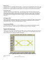
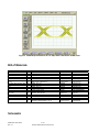
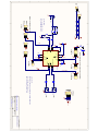
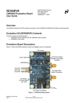
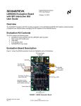
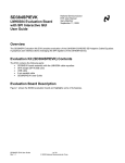
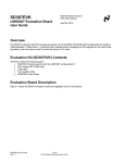
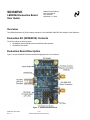
SD384EVK
LMH0384 Evaluation Board
User Guide
National Semiconductor
EVK User Manual
Gary Melchior
September 11, 2009
Overview
The SD384 Evaluation Kit (EVK) enables evaluation of the LMH0384 3G/HD/SD SDI Adaptive Cable Equalizer.
Evaluation Kit (SD384EVK) Contents
The EVK contains the following parts:
• SD384EVK board assembly with the LMH0384 cable equalizer
• SD384EVK User Guide
Evaluation Board Description
Figure 1 shows the SD384 evaluation board and highlights some of its features.
Figure 1. SD384 Evaluation Board
SD384 EVK User Guide
Rev 1.2
1 of 5
© 2009, National Semiconductor Corp.
SDI Input and SDO Output
The SDI input connector (J1) is a 75Ω BNC connector. The SDI input should conform to the SMPTE 424M,
SMPTE 292M, or SMPTE 259M standards.
The SDO output connectors (J2 and J3) are 50Ω SMA connectors. When using only one side of the output pair,
the other side should be terminated with a 50Ω SMA termination. For example, when only using the SDO output,
¯¯¯¯
SDO should be terminated with a 50Ω SMA termination.
DC Power Connectors
The VCC and GND power connectors should be powered with a DC input voltage of 3.3V ± 5% (3.6V maximum).
SPI Mode / Pin Mode Select (JP1 – JP4)
JP1, JP2, JP3, and JP4 are used to select between SPI Mode or Pin mode. To select Pin Mode, set four jumpers
as shown in Figure 2, and to select SPI Mode, set four jumpers as shown in Figure 3. Either Pin Mode or SPI
mode must be selected for proper operation; do not leave JP1-JP4 open.
Figure 2. Pin Mode Select
Figure 3. SPI Mode Select
MUTEREF (JP5)
JP5 allows control of the MUTEREF function and may be used in either Pin Mode or SPI Mode. MUTEREF is an input
voltage used to set the threshold for ¯¯¯
CD . The MUTEREF DC input voltage should be between 0V and 3.3V. Refer
to the LMH0384 datasheet for details. Leave JP5 unconnected for normal operation.
Pin Mode Controls (JP6 – JP8)
JP6, JP7, and JP8 are used to control LMH0384 features while the device is configured for Pin Mode. Jumpers
should not be placed on JP6, JP7, or JP8 while the device is configured for SPI Mode.
¯¯¯
CD and MUTE (JP6)
¯¯¯ ) monitoring and MUTE control. ¯¯¯
JP6 allows Carrier Detect (CD
CD is high when no input signal is present. MUTE
may be used to force the outputs on or off, or tied to ¯¯¯
CD to allow automatic mute operation based on the input
signal. To activate mute and force the outputs into a muted condition, set the jumper to pull MUTE to VCC. To turn
off mute so that the outputs will never mute, set the jumper to tie MUTE to GND. For normal operation, set the
jumper to tie ¯¯¯
CD to MUTE for automatic mute control. The LMH0384 MUTE pin has an internal pulldown (to
disable mute), so JP6 may be left unconnected and the LMH0384 will never mute.
SD384 EVK User Guide
Rev 1.2
2 of 5
© 2009, National Semiconductor Corp.
BYPASS (JP7)
JP7 allows control of the equalization BYPASS function. To put the device into bypass mode, set the jumper to pull
BYPASS to VCC. To turn off bypass (for normal operation) set the jumper to pull BYPASS to GND. The LMH0384
BYPASS pin has an internal pulldown (to disable bypass), so JP7 may be left unconnected for normal operation.
AUTO SLEEP (JP8)
JP8 allows control of the AUTO SLEEP function. To put the device into auto sleep mode in which it will power
down when no input is detected, set the jumper to pull AUTO SLEEP to VCC. To turn off auto sleep and prevent
the LMH0384 from automatically powering down, set the jumper to pull AUTO SLEEP to GND. The LMH0384
AUTO SLEEP pin has an internal pullup (to enable auto sleep), so JP8 may be left unconnected to enable auto
sleep mode.
SPI Header (JP9)
JP9 is the SPI (Serial Peripheral Interface) header. It allows access to the SPI pins (¯¯¯
SS , MISO, MOSI, and SCK)
while the LMH0384 is in SPI mode. These pins may be connected to a standard SPI controller to access the
LMH0384 SPI registers. Refer to the LMH0384 datasheet for details.
Carrier Detect LED (D1)
D1 shows the status of Carrier Detect. This LED is GREEN when an input signal has been detected, and OFF
when no input is detected. D1 shows the status of Carrier Detect while in Pin Mode or SPI Mode.
Typical Performance
Figures 4 and 5 show typical output waveforms of the SD384, with the 1m of Belden 1694A cable on the input and
110m of Belden 1694A cable on the input, respectively. The input signal is a 2.97 Gbps PRBS10, and the output
signal is measured on the Agilent DCA-J 86100C Oscilloscope.
Figure 4. SD384 Output Waveform at 2.97 Gbps with 1m Belden 1694A Cable
SD384 EVK User Guide
Rev 1.2
3 of 5
© 2009, National Semiconductor Corp.
Figure 5. SD384 Output Waveform at 2.97 Gbps with 110m Belden 1694A Cable
Bill of Materials
Reference Designator
C1, C7, C8
C2, C3, C4
C5, C6, C14, C16, C17
D1
J1
Qty
3
3
5
1
1
Description
Capacitor, 4.7uF, 6.3V, X5R, 0603
Capacitor, 1uF, 6.3V, X5R, 0402
Capacitor, 0.1uF, 16V, X5R, 0402
LED, Green, 0603
BNC, Amphenol, 75-ohm, edge launch
J2, J3
JP1, JP2, JP3, JP4, JP7, JP8
JP5
JP6
JP9
L1
2
6
1
1
1
1
PS1, PS2
R1, R2
R5
R4
2
2
1
1
SMA, 50-ohm, edge launch
Header, 3x1, 0.1"
Header, 2x1, 0.1"
Header, 3x2, 0.1"
Header, 6x1, 0.1"
Inductor, 5.6nH, 0402
PCB Quick-Fit Male Terminal, .052"
diameter, .250" tab size
Resistor, 75-ohm, 1/16W, 1%, 0402
Resistor, 37.4-ohm, 1/16W, 1%, 0402
Resistor, 300-ohm, 1/10W, 5%, 0402
U1
1
LMH0384 Cable Equalizer, LLP-16
Schematic
SD384 EVK User Guide
Rev 1.2
4 of 5
© 2009, National Semiconductor Corp.
Manufacturer
Panasonic - ECG
Panasonic - ECG
Panasonic - ECG
Lite-On
Amphenol
Johnson
Components
3M/ESD
3M/ESD
3M/ESD
3M/ESD
Murata
Keystone
Electronics
Yageo
Vishay/Dale
Panasonic - ECG
National
Semiconductor
Manufacturer Part No.
ECJ-1VB0J475M
ECJ-0EB0J105M
ECJ-0EB1C104K
LTST-C190GKT
31-6009
142-0701-851
929834-02-36
929834-02-36
929836-02-36
929834-02-36
LQP15MN5N6B02D
1287-ST
RC0402FR-0775RL
CRCW040237R4FKED
ERJ-2GEJ301X
LMH0384SQ
GND
PS2
2
1
PS1
2
1
SDI
J1
C1
4.7uF
Z75_1
BNC_EDGE
C14
0.1uF
L1
5.6nH
2
C16
0.1uF
C15
open
R1
75
JP2
1
2
3
VCC
C17
0.1uF
GND
C2
1uF
C3
1uF
BYPASS
CD
GND
R5
37.4
Z75_2
R2
75
HDR_3
VCC
GND
Z75_3
Z75_4
JP3
1
2
3
HDR_3
R4
300
C5
0.1uF
CD
GND
CD
D1
JP6
1
3
5
VEE
SDI
SDI
SPI_EN
3
VCC
C4
1uF
JP4
1
2
3
HDR_3
GND
VCC
GND
GND
JP7
1
2
3
HDR_3
BYPASS
C6
0.1uF
U1
LMH0384
12
11
10
9
MUTEREF
HDR_2
1
2
JP5
VEE/SS
SDO
SDO
AUTOSLP/MISO
GND
VCC
GND
BYPASS
VCC
4
JP8
1
2
3
HDR_3
4
C7
4.7uF
C8
4.7uF
JP9
SPI Header
5
SDO+
GND
J2
SMA_R_EDGE
SDO-
GND
SCK
MOSI
MISO
SS
GND
1
2
3
4
5
6
Z50_1
J3
SMA_R_EDGE
HDR_6
Z50_2
GND
Z50_1, Z50_2: W=40MIL, ZO=50+-5%
SMA: 3/4 inch spacing, center to center
5
MUTE/SCK
MOSI
AUTOSLP/MISO
VEE/SS
Doc No.
File: C:\SD384\LMH0344.SchDoc
Print Date: 3/4/2009
Size: B
Sheet 1
of 1
Rev: A
SD384 Evaluation Board for LMH0384
Title
ZDIFF100_P, ZDIFF100_N: DIFFERENTIAL 100OHM IMPEDANCE
LAYOUT NOTE:
ZDIFF100_N
ZDIFF100_P
AUTO SLEEP
GND
VCC
Pin Mode Controls (do not place Jumpers JP6-8 for SPI Mode)
2
4
6
HDR_3X2
CD/MUTE
LED
1
2
3
4
MOSI
CD/MOSI
CD
3
AUTOSLP/MISO
1
VCC
GND
VCC
GND
MUTE/SCK
8
LAYOUT NOTE:
Z75_1: W=20MIL, ZO=75+-5%
Z75_2: W=20MIL, ZO=75+-5%
JP1
1
2
3
SPI Mode / Pin Mode Select (JP1-JP4)
SPI Mode
Pin Mode
SPI_EN
HDR_3
2
VEE/SS
13
VCC
CD/MOSI
MUTEREF
MUTEREF
15
14
MUTE/SCK
7
BYPASS/CD
BYPASS/CD
CD/MOSI
16
VCC
AEC6
AEC+
5
17
DAP
A
B
C
D
1
SPI_EN
6
Company Confidential
National Semiconductor
6
A
B
C
D