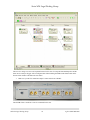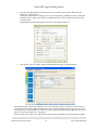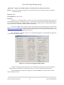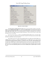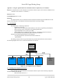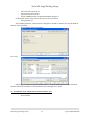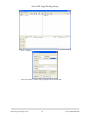
1
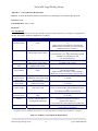
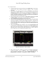
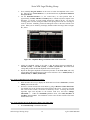
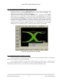
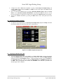
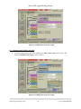
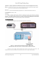
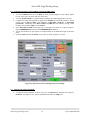
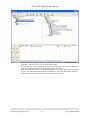
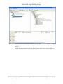
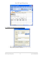
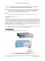
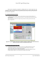
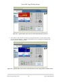
Serial ATA
International Organization
Version 1.00RC
29-May 2008
Serial ATA Interoperability Program Revision 1.3
Agilent MOI for SATA RSG Tests
This document is provided "AS IS" and without any warranty of any kind, including, without limitation, any express
or implied warranty of non-infringement, merchantability or fitness for a particular purpose. In no event shall
SATA-IO or any member of SATA-IO be liable for any direct, indirect, special, exemplary, punitive, or
consequential damages, including, without limitation, lost profits, even if advised of the possibility of such
damages.
This material is provided for reference only. The Serial ATA International Organization does not endorse the vendor
equipment outlined in this document.
Serial ATA Logo Working Group
TABLE OF CONTENTS
TABLE OF CONTENTS .........................................................................................2
MODIFICATION RECORD ..................................................................................3
ACKNOWLEDGMENTS .......................................................................................5
INTRODUCTION....................................................................................................6
GROUP 1: RSG REQUIREMENTS ......................................................................7
TEST RSG-01: GEN1 (1.5GB/S) RECEIVER JITTER TOLERANCE TEST .......................................... 8
TEST RSG-02: GEN2 (3.0GB/S) RECEIVER JITTER TOLERANCE TEST .......................................... 9
APPENDICES ........................................................................................................10
APPENDIX A – GENERAL RESOURCE REQUIREMENTS ................................................................ 11
APPENDIX B – SSG CALIBRATION PROCEDURE (USING AGILENT DSO81204 REAL-TIME DSO
AS THE JMD) ............................................................................................................................. 14
APPENDIX C – SSG CALIBRATION PROCEDURE (USING AGILENT N4903A J-BERT AS THE JMD)
(INFORMATIVE) .......................................................................................................................... 18
APPENDIX D – SSG CALIBRATION PROCEDURE (USING AGILENT 86100C DCA-J AS THE JMD)
(INFORMATIVE) .......................................................................................................................... 20
APPENDIX E – USING THE AGILENT N4903A J-BERT (FW V4.91 OR LATER) AS THE STRESSED
SIGNAL GENERATOR (SSG)........................................................................................................ 25
APPENDIX F – USING THE AGILENT 81133/4A PULSE/PATTERN GENERATOR AS THE STRESSED
SIGNAL GENERATOR (SSG)........................................................................................................ 28
APPENDIX G – USING THE AGILENT N4219B SERIAL ATA PROBE AS THE FRAME ERROR
DETECTOR ................................................................................................................................. 31
APPENDIX H – USING THE CRESCENT HEART SOFTWARE SATA-II PROBE AS THE FRAME ERROR
DETECTOR ................................................................................................................................. 37
APPENDIX I – SUGGESTED INITIAL AMPLITUDE AND DJ/RJ SETTINGS FOR VARIOUS SSG SETUPS
(INFORMATIVE) .......................................................................................................................... 39
APPENDIX J – USING THE AGILENT N5990A TEST AUTOMATION SOFTWARE OPTION 103 (A.K.A.
VALIFRAME)............................................................................................................................... 40
APPENDIX K – USING THE AGILENT 81133/4A PULSE/PATTERN GENERATOR AND 81150A PULSE
FUNCTION ARBITRARY NOISE GENERATOR AS THE STRESSED SIGNAL GENERATOR (SSG)
(INFORMATIVE) .......................................................................................................................... 46
SATA-IO Logo Working Group
2
Agilent SATA RSG MOI
Serial ATA Logo Working Group
MODIFICATION RECORD
(REVISIONS FOR 1.3 INTEROP PROGRAM)
2008 May 29 (Version 1.00RC) MINOR UPDATE FOLLOWING MAY 29 LOGO WG REVIEW AND APPROVAL
Andy Baldman (UNH-IOL): RSG-01: Removed footnote in procedure Step 11 regarding the previous J-BERT limitation for Gen1/62MHz.
Appendix A: Added footnote to Table A-1 stating that v4.91 FW or newer is required to use J-BERT.
Appendix E: Removed Informative status from appendix Title.
Appendix E: Added text to appendix Title and Discussion stating v4.91 FW or newer is required to use J-BERT.
2008 Feb 10 (Version 0.90) MINOR UPDATE FOLLOWING FEB 8 LOGO WG REVIEW
Andy Baldman (UNH-IOL): Appendix A: Added note to bottom of Table A-1 denoting current status of 81150A generator as informative.
2008 Feb 07 (Version 0.85) MAJOR UPDATE TO SUPPORT REVISION 1.3 INTEROP PROGRAM
Andy Baldman (UNH-IOL): Entire Document: Updated all UTD references to point to r1.3 UTD.
Entire Document: Updated all spec references to point to SATA v2.6.
RSG-01 and RSG-02: Added 5MHz DJ test case to procedure.
Appendix A: Added Agilent 81150A DJ/RJ Signal Generator to Table A-1.
Appendix A: Added Agilent N4915A Serial Bus Switches to Table A-1.
Appendix A: Added CHS TF-eSATA-NE-ZP fixture to Table A-1.
Appendix A: Updated Figure A-1 to show new setup using N4915A Serial Bus Switches.
Appendix A: Modified Figure A-2 to make RJ + DJ sources generic.
Appendix A: Replaced A.3 and Figure A-3 (cal setup diagram) with modified Valiframe setup.
Appendix A: Replaced all references to power splitters with Serial Bus Switches
Appendix B: Changed wording in B.2 to point to Figure A-1 for setup.
Appendix B: Added gen1m/2m levels to B.2 amplitude calibration procedure.
Appendix B: Changed B.5 jitter text to indicate inclusion of m-level PUTs.
Appendix B: Added 5MHz to B.7 list of DJ frequencies.
Appendix C: Filled out C.5 (previously TBD) with TJ/DJ measurement procedure.
Appendix C: Added 5MHz to C.7 list of DJ frequencies.
Appendix D: Added gen1m/2m levels to D.2 and D.7.
Appendix E: Deleted reference to resistive splitters in E.1.
Appendix F: Changed Figure F-1 to only show SSG components.
Appendix F: Removed splitters from Figure F-1, and deleted text from F.1 discussing splitter use.
Added new informative Appendix K for using Agilent 81150A as DJ/RJ source.
(PREVIOUS REVISIONS FOR 1.2 INTEROP PROGRAM)
2007 Oct 24 (Version 1.00) FINAL APPROVED r1.2 RELEASE
Andy Baldman (UNH-IOL): Cover Page: Updated document version number to 1.00.
2007 Jul 12 (Version 1.00RC1) EDITORIAL UPDATE FOLLOWING 12JUL2007 RC APPROVAL
Andy Baldman (UNH-IOL): Cover Page: Updated document version number to 1.00RC.
2007 Jun 07 (Version 0.92) ADDITIONAL UPDATES, POST-IW3
Andy Baldman (UNH-IOL): Acknowledgements page: Added Hermann Stehling, for Bitifeye contributions of automation software.
RSG-01 and RSG-02: Added note at bottom of procedure to cover premature test abortion for cases when
excessive errors are observed (i.e., >1000) for any test case, as per the UTD.
Appendix A: Added Agilent SMA cables and part numbers to equipment list.
Appendix A: Added model numbers of suitable equivalent Noisecom sources to equipment list.
Appendix A: Added E4432B sine source to equipment list as suitable DJ source.
Appendix I: Added initial starting settings for using E4432B as DJ source with 81134A SSG.
Added new Appendix (Appendix J), for Bitifeye automation software.
SATA-IO Logo Working Group
3
Agilent SATA RSG MOI
Serial ATA Logo Working Group
2007 Apr 28 (Version 0.90) MINOR UPDATES IN RESPONSE TO 17APR2007 REVIEW.
Andy Baldman (UNH-IOL): Cover Page: Updated SATA logo to trademarked version, and added CHS Frame Error Detector.
Entire Document: Changed Noisecom noise source model name from UFX-7110 to PNG-7110.
Appendix A: Changed amplitude procedure BACK to using LBP lone 0/1, rather than ALIGN minimum
amplitude bits.
Renamed Appendix H to Appendix I.
Added new Appendix H for Crescent Heart Software Frame Error Detector.
2007 Apr 16 (Version 0.88) ADDITIONAL MAJOR UPDATES
Andy Baldman (UNH-IOL): Entire Document: Updated all DJ references to .270UI, from .320UI.
Entire Document: Removed all references to using 14dB splitters. (50/50 splitters are preferred, for
better return loss and matching.)
Appendix A: Changed amplitude procedure to use ALIGN Minimum Amplitude Bit instead of LBP lone bit.
Appendix D: Cleaned up many typos, and moved J-BERT-specific SSG info into Appendix E.
2007 Apr 08 (Version 0.87) MAJOR UPDATE FOR REVISION 1.2 INTEROP PROGRAM
Andy Baldman (UNH-IOL): Entire document: Updated all UTD and MOI references to reflect Program Revision 1.2
RSG-01/02: Changed DJ frequencies from 5/10/62MHz to 10/33/62MHz per UTD updates.
Appendix A: Added 14dB pickoff tees to Table A-1, and changed Figure A-3 to a block diagram.
Appendix B: Completely overhauled, adding procedure for amplitude calibration using isolated Lone 1.
Appendices C, D, E: Made informative.
Appendix F: Major rewrite to include procedure for using Noisecom PNG-7110 noise source.
(PREVIOUS REVISIONS FOR 1.0 AND 1.1 INTEROP PROGRAMS)
2006 Nov 23 (Version 0.85) ADDITIONAL UPDATES
Michael Herz (Agilent):
Added contents on an 81134A-based setup.
2006 Nov 22 (Version 0.84) ADDITIONAL MAJOR UPDATES
Andy Baldman (UNH-IOL): Created separate appendices for J-BERT, DCA-J, and real-time DSO calibration.
Created separate appendix for using 81134A-based setup (instead of J-BERT) for jitter generation.
Renumbered all Appendices as a result of above changes.
RSG-01/02: Replaced ‘Pattern Generator’ with ‘SSG’, to make more modular, and hardware independent.
2006 Nov 13 (Version 0.83) FIRST MAJOR UPDATE
Andy Baldman (UNH-IOL): Updated title page to new revision 1.1 naming conventions.
Added procedures to Appendix B to support multiple Jitter Measurement Devices for calibration purposes.
Added Appendix C for SATA Probe setup and configuration.
2006 Sep 24 (Version 0.81) INITIAL DRAFT RELEASE
Andy Baldman (UNH-IOL): Initial Release
SATA-IO Logo Working Group
4
Agilent SATA RSG MOI
Serial ATA Logo Working Group
ACKNOWLEDGMENTS
The Serial ATA Logo Working Group would like to acknowledge the efforts of the
following individuals in the development of this document:
David Woolf
Andy Baldman
Dr. Michael Herz
Hermann Stehling
SATA-IO Logo Working Group
UNH InterOperability Lab
UNH InterOperability Lab
Agilent Technologies
Bitifeye Digital Test Solutions
5
[email protected]
[email protected]
[email protected]
[email protected]
Agilent SATA RSG MOI
Serial ATA Logo Working Group
INTRODUCTION
The tests contained in this document are organized in order to simplify the identification of information
related to a test, and to facilitate in the actual testing process. Tests are separated into groups, primarily in order to
reduce setup time in the lab environment, however the different groups typically also tend to focus on specific
aspects of product functionality.
The test definitions themselves are intended to provide a high-level description of the motivation,
resources, procedures, and methodologies specific to each test. Formally, each test description contains the
following sections:
Purpose
The purpose is a brief statement outlining what the test attempts to achieve. The test is written at the
functional level.
References
This section specifies all reference material external to the test suite, including the specific subclauses
references for the test in question, and any other references that might be helpful in understanding the test
methodology and/or test results. External sources are always referenced by a bracketed number (e.g., [1]) when
mentioned in the test description. Any other references in the test description that are not indicated in this manner
refer to elements within the test suite document itself (e.g., “Appendix 6.A”, or “Table 6.1.1-1”)
Resource Requirements
The requirements section specifies the test hardware and/or software needed to perform the test. This is
generally expressed in terms of minimum requirements, however in some cases specific equipment
manufacturer/model information may be provided.
Last Modification
This specifies the date of the last modification to this test.
Discussion
The discussion covers the assumptions made in the design or implementation of the test, as well as known
limitations. Other items specific to the test are covered here as well.
Test Setup
The setup section describes the initial configuration of the test environment. Small changes in the
configuration should not be included here, and are generally covered in the test procedure section (next).
Procedure
The procedure section of the test description contains the systematic instructions for carrying out the test.
It provides a cookbook approach to testing, and may be interspersed with observable results.
Observable Results
This section lists the specific observables that can be examined by the tester in order to verify that the PUT
is operating properly. When multiple values for an observable are possible, this section provides a short discussion
on how to interpret them. The determination of a pass or fail outcome for a particular test is generally based on the
successful (or unsuccessful) detection of a specific observable.
Possible Problems
This section contains a description of known issues with the test procedure, which may affect test results in
certain situations. It may also refer the reader to test suite appendices and/or other external sources that may provide
more detail regarding these issues.
SATA-IO Logo Working Group
6
Agilent SATA RSG MOI
Serial ATA Logo Working Group
GROUP 1: RSG REQUIREMENTS
Overview:
This group of tests verifies receiver functionality under stressed-signal conditions, for the
purposes of performing SATA-IO Interoperability Program testing. These tests are limited to
functionality which are covered by tests RSG-01 and RSG-02 (Section 2.16 of the Serial ATA
Interoperability Program Unified Test Document Revision 1.3), and do not provide
comprehensive coverage of all receiver tolerance requirements defined by the SATA Revision
2.6 standard.
SATA-IO Logo Working Group
7
Agilent SATA RSG MOI
Serial ATA Logo Working Group
Test RSG-01: Gen1 (1.5Gb/s) Receiver Jitter Tolerance Test
Purpose: To verify that the receiver of the Product Under Test (PUT) can operate without error under stressed
signal conditions while operating at 1.5Gb/s.
References:
[1] SATA Interoperability Program Revision 1.3 Unified Test Document, Section 2.16.1
[2] SATA Interoperability Program Revision 1.3 Pre-Test MOI, Appendix B (Framed COMP Pattern)
Resource Requirements: See Appendix A.
Last Modification: May 29, 2008
Discussion: Reference [1] specifies the basic requirements for Receiver Jitter Tolerance testing for the purposes of
the SATA-IO Interoperability Program. These requirements are a subset of the complete set of requirements defined
in the SATA standard. Note that this test requirement is only applicable to products running at 1.5Gb/s. For
products that support 3.0Gb/s, this test is not required.
Test Setup: See Appendix A.
Test Procedure:
Note this test procedure assumes the user has already performed the initial system setup and calibration
procedures outlined in Appendices A-K of this document.
1) Connect the PUT to the test system as outlined in Appendix A.
2) Configure the N4915A Serial Bus Switches so that the TX and RX pairs of the PUT are connected to the
BIST Configuration Tool.
3) Configure the Stressed Signal Generator (SSG) to send the Framed COMP pattern [2] at 1.5Gb/s, and turn
the output of the generator OFF (i.e., disable all signal output).
4) Configure the PUT for BIST-L operation at 1.5Gb/s using the BIST Configuration Tool.
5) Turn the output of the SSG ON, but with jitter disabled (i.e., clean pattern with nominal SATA amplitude).
6) Activate the N4915A Switches so that the PUT RX is connected to the SSG, and its TX is connected to the
Frame Error Counter.
7) Verify using the Frame Error Counter that the PUT is properly looping back the unstressed Framed COMP
pattern data without error.
8) Configure the SSG for Sinusoidal DJ at a frequency of 5MHz, with the proper DJ, RJ, and Amplitude
values determined during the cal procedure for 1.5Gb/s operation. Enable jitter generation on the SSG
output, and turn the SSG output ON.
9) Reset the counter on the Frame Error Counter.
10) Run the test for 20 minutes and record the number of frame errors detected by the Frame Error Counter.
11) Repeat steps 8-10 for the 10, 33, and 62 MHz sinusoidal jitter frequencies.
Note that for any jitter frequency test case, if ‘excessive’ errors are observed (i.e., >1000), the test may be
prematurely aborted, and a failing result assigned for that test case.
Observable Results:
• For all 4 sinusoidal jitter frequencies, the number of frame errors observed should be zero.
Possible Problems: None
SATA-IO Logo Working Group
8
Agilent SATA RSG MOI
Serial ATA Logo Working Group
Test RSG-02: Gen2 (3.0Gb/s) Receiver Jitter Tolerance Test
Purpose: To verify that the receiver of the Product Under Test (PUT) can operate without error under stressed
signal conditions while operating at 3.0Gb/s.
References:
[1] SATA Interoperability Program Revision 1.3 Unified Test Document, Section 2.16.2
[2] SATA Interoperability Program Revision 1.3 Pre-Test MOI, Appendix B (Framed COMP Pattern)
Resource Requirements: See Appendix A.
Last Modification: February 5, 2008
Discussion: Reference [1] specifies the basic requirements for Receiver Jitter Tolerance testing for the purposes of
the SATA-IO Interoperability Program. These requirements are a subset of the complete set of requirements defined
in the SATA standard. Note that this test applies only to products operating at 3.0Gb/s.
Test Setup: See Appendix A.
Test Procedure:
Note this test procedure assumes the user has already performed the initial system setup and calibration
procedures outlined in Appendices A-K of this document.
1) Connect the PUT to the test system as outlined in Appendix A.
2) Configure the N4915A Serial Bus Switches so that the TX and RX pairs of the PUT are connected to the
BIST Configuration Tool.
3) Configure the Stressed Signal Generator (SSG) to send the Framed COMP pattern [2] at 1.5Gb/s, and turn
the output of the generator OFF (i.e., disable all signal output).
4) Configure the PUT for BIST-L operation at 3.0Gb/s using the BIST Configuration Tool.
5) Turn the output of the SSG ON, but with jitter disabled (i.e., clean pattern with nominal SATA amplitude).
6) Activate the N4915A Switches so that the PUT RX is connected to the SSG, and its TX is connected to the
Frame Error Counter.
7) Verify using the Frame Error Counter that the PUT is properly looping back the unstressed Framed COMP
pattern data without error.
8) Configure the SSG for Sinusoidal DJ at a frequency of 5MHz, with the proper DJ, RJ, and Amplitude
values determined during the cal procedure for 3.0Gb/s operation. Enable jitter generation on the SSG
output, and turn the SSG output ON.
9) Reset the counter on the Frame Error Counter.
10) Run the test for 20 minutes and record the number of frame errors detected by the Frame Error Counter.
11) Repeat steps 8-10 for the 10, 33, and 62 MHz sinusoidal jitter frequencies.
Note that for any jitter frequency test case, if ‘excessive’ errors are observed (i.e., >1000), the test may be
prematurely aborted, and a failing result assigned for that test case.
Observable Results:
• For all jitter frequencies, the number of frame errors observed should be zero.
Possible Problems: None
SATA-IO Logo Working Group
9
Agilent SATA RSG MOI
Serial ATA Logo Working Group
APPENDICES
Overview:
Test suite appendices are intended to provide additional low-level technical detail
pertinent to specific tests contained in this test suite. These appendices often cover topics that
are outside of the scope of the standard, and are specific to the methodologies used for
performing the measurements in this test suite. Appendix topics may also include discussion
regarding a specific interpretation of the standard (for the purposes of this test suite), for cases
where a particular specification may appear unclear or otherwise open to multiple interpretations.
Test suite appendices are considered informative supplements, and pertain solely to the
test definitions and procedures contained in this test suite.
SATA-IO Logo Working Group
10
Agilent SATA RSG MOI
Serial ATA Logo Working Group
Appendix A – General Resource Requirements
Purpose: To define the hardware/software requirements for performing the tests defined in this document.
References: None.
Last Modification: May 29, 2008
Discussion:
A.1 - Introduction
In order to perform receiver jitter tolerance testing on SATA transceivers, several pieces of equipment are
needed. The primary functional components are as follows:
Component
Stressed Signal
Generator (SSG)
Function
Generates jittered/stressed test
signal
RJ Noise Source
Used as RJ modulation source
(when using 81134A as SSG.)
DJ Sine Source
BIST Configuration
Tool
Jitter Measurement
Device (JMD)
Used as DJ modulation source
(when using 81134A as SSG.)
Used to enable BIST-L
loopback mode of PUT
Used to verify/calibrate SSG
output.
3-Way, 50/50
Resistive Power
Splitter (PS)
Hi-Speed Serial Bus
Switch (HSS)
Frame Error
Counter (FERC)
Used to combine DJ+RJ
modulation sources when using
81134A as SSG
Used to mux BIST Generator in
and out of test setup.
Used to detect and count frame
errors on PUT TX
Transition Time
Converters (TTC)
SATA-to-SMA Test
Fixture
Used to create SSG risetime of
100ps
Used to convert SATA
interface of PUT to SMA, for
test instrument connections
SMA Test Cables
Used for all connections
Device/Model
Agilent N4903 J-BERT (v4.91 FW or newer)*
or,
Agilent 81133A (one channel) or 81134A (two
channels) Pattern Generator, plus external DJ/RJ
modulation sources (see below).
Agilent 81150A**
or,
NoiseCom PNG-7110. (Equivalent models include
UFX/PNG-7107/08/09/10/12, and
NC-6107/08/09/10/12)
Agilent 81150A**, or 33250A,
or E4432B signal generator
PC running Ulink DriveMaster software
Agilent Infiniium DSO81304A 13GHz Real-Time
DSO (Recommended)
(Agilent 86100C w 54754A, or Agilent N4903 JBERT may be used for informative purposes only.)
Agilent 11636B or equivalent
(1 needed)
Agilent N4915A-005
(2 needed)
Agilent 168xx or 169xx Logic Analyzer with 16910,
16911, or 16950 module, and N4219B SATA Probe.
or,
Crescent Heart Software SATA-II Probe
Agilent N15435A
(2 needed)
Comax P/N H303000204A, or
Crescent Heart TF-SATA-NE-XP, or
Agilent N5421-26401, or
Crescent Heart TF-eSATA-NE-ZP (for Gen1m/2m)
Agilent 15442-61601 (includes 4 cables)
14 total cables recommended.
* Starting with firmware v4.91, all jitter frequencies are supported by J-BERT.
** Agilent 81150A is considered informative for r1.3, and is expected to be formally approved under the r1.4 program.
Table A-1: Summary of Test Hardware Requirements
SATA-IO Logo Working Group
11
Agilent SATA RSG MOI
Serial ATA Logo Working Group
A.2- Basic Test Setup
Figure A-1 shows a Test Setup that supports both disconnect and non-disconnect PUT’s. The BIST
Configuration Tool is multiplexed into the TX and RX pairs of the PUT using the N4914A-005 Serial Bus Switches,
which allow non-disconnect-supporting PUT’s to be put into BIST-L using the BIST Configuration Tool, then be
sent the framed COMP test pattern into their RX from the SSG while being monitored on the TX by the Frame Error
Counter. Once the PUT is placed into BIST-L loopback mode, the BIST Configuration Tool is effectively switched
out of the system in order to run the formal test.
Figure A-1: Basic Test Configuration
Figure A-2 illustrates how either the (a) Agilent 81133/4A pulse/pattern generator or (b) Agilent N4903A
J-BERT may be used as the SSG. If the J-BERT is used as the SSG, no additional sources are required. The setup
using the 81133/4A requires two external sources to generate jitter. The outputs of the DJ and RJ modulation
sources are combined through a power divider into the 81133/4A’s Delay Control Input.
SATA-IO Logo Working Group
12
Agilent SATA RSG MOI
Serial ATA Logo Working Group
Figure A-2: (a) Use of Agilent 81133/4A, or (b) Agilent N4903A J-BERT (Gen2 only) as the SSG
A.3- Modified Setup for use with Valiframe Automation Software
Figure A-3 shows a modified version of the basic setup from Figure A-1, which is to be used when using
the Valiframe automation software in conjunction with the N4915A-005 Serial Bus Switches.
Figure A-3: Modified Setup for Switch Automation When Using Valiframe Software
SATA-IO Logo Working Group
13
Agilent SATA RSG MOI
Serial ATA Logo Working Group
Appendix B – SSG Calibration Procedure (using Agilent DSO81204 Real-Time DSO as the JMD)
Purpose: To define a procedure for verification and calibration of the stressed signal generator setup, using the
Agilent Infiniium DSO81204 (or equivalent 80000-series DSO) as the Jitter Measurement Device.
References:
[1] Serial ATA Interoperability Program Revision 1.3 Unified Test Document, Section 2.16
Last Modification: February 7, 2008
Discussion:
Prior to running the actual stressed receiver tests, it is necessary to perform several steps to verify and
calibrate the test system, in order to ensure that the signal delivered to the receiver of the PUT exhibits the proper
type and amount of stress for the each test, as defined in [1].
First, we must verify that the SSG is providing the proper amounts of TJ and RJ at the reference plane.
Note that the reference plane in this case is the end of the SMA cables, where they connect to the fixture that
interfaces to the PUT.
The setup and calibration procedure is as follows:
B.1 - Configure the SSG to send the Framed COMP signal:
•
See Sections E.2 (for J-BERT) or F.2 (for 81134A) of this MOI.
B.2 - Calibrate the Differential Amplitude at the Reference Plane:
The amplitude calibration procedure requires measuring the amplitude of two particular bits contained in
the framed COMP pattern, namely the Lone 0 and Lone 1 bits contained in the SATA Lone Bit Pattern (LBP).
Performing this measurement requires isolating these bits on the scope so that the amplitude of only those bits
can be measured. To do this, we will use a reference signal from the SSG, which is synchronized to the start of
the Framed COMP pattern, as a trigger reference to trigger the scope. The delay can then be adjusted to isolate
the desired bits, perform the amplitude measurement, and adjust accordingly.
This procedure assumes that the SSG possesses a trigger out signal, which can output a rising edge at the
beginning of the pattern. (For details regarding particular SSG’s, refer to Appendices E (J-BERT) and F
(81134A) of this MOI.)
First, we will set up and connect the hardware:
•
•
•
Connect the Trigger Out signal of the SSG to the Channel 4 input of the DSO.
Using the diagram in Appendix A, Figure A-1 as a guide, configure the system so that
the SSG is transmitting through the switches and into the DSO (which should be
connected to the “C” ports of the uppermost switch.)
Load the Framed COMP pattern into the SSG, and set the initial amplitude. (See E.2
for J-BERT and F.2 for 81134A).
SATA-IO Logo Working Group
14
Agilent SATA RSG MOI
Serial ATA Logo Working Group
Next, configure the DSO:
•
•
•
•
•
•
Assuming the DSO has been properly deskewed, press Default Setup to reset the DSO.
Connect the TX+ and TX- outputs of the SSG to Channels 1 and 3 of the DSO,
respectively.
On the DSO, create a math waveform (CH1-CH3) on Function 4 for the differential
signal by going to Analyze->Math to set up the function. Select the f4 function, click
the Display On checkbox (so it is selected), then select Subtract in the Operator menu,
then select Channel 1 for Source 1, and Channel 3 for Source 2. Click Close, then
manually turn off the individual Channels 1 and 3 using the front panel hard buttons so
that only the math waveform remains on the screen.
On the front panel trigger setup of the DSO, set Trigger Mode to Edge, Source to CH4,
and Slope to Positive. Set the trigger level to 0mV using the front panel knob.
Turn the Channel 4 display ON using the front panel “4” button.
Using the front panel Vertical Gain knobs, scale Channels 1 and 3 so they span as much
of the screen as possible. Keep the same setting for both channels. Then turn both
channel displays OFF using the front panel “1” and “3” buttons. You should now see
the rising edge trigger pulse on Channel 4, and the differential math waveform. Once
you have verified that you have a stable trigger on CH4, turn the CH4 display OFF using
the front panel button.
Set the scope’s Horizontal setting to 2ns/div. Then, using the Horizontal Delay knob
on the front panel, scroll through the waveform until you see the Lone 1 pattern, shown
below. (Note you may have to scroll for a while until you see it. It is a 00001000 pattern
followed by 110 110. Look for the lone “spike” followed by two “fangs”.) When you
have it isolated on the screen, it should look like Figure B-2, below.
Figure B-2: Isolated Lone 1 and Lone 0 Bits
•
Once you have the Lone 1 isolated, we will now do a histogram measurement to
determine the amplitude. Zoom in to 200ps/div. Then go to Analyze->Histogram to
open the histogram configuration screen. Check the Enable Histogram box. Set
Histogram Source to Waveform. Set Orientation to Vertical. Then hit Close.
SATA-IO Logo Working Group
15
Agilent SATA RSG MOI
Serial ATA Logo Working Group
•
•
Now, manually drag the markers on the screen to isolate the amplitude of the Lone 1
bit. Move the two vertical markers (i.e., the horizontal bars) to just above and below
the top of the bit.
For the horizontal markers (i.e., the vertical bars), we must position them at
approximately the 40% and 60% UI width points, to include only those samples in the
histogram. To do this, we must roughly measure the width of the bit. Use the zero
crossing points to do this, noting the width of the spacing between the zero crossings in
terms of divisions. Manually position the histogram cursors at the 40% and 60% time
points. When you are finished, your display should resemble the image shown in Figure
B-3, below.
Figure B-3: Amplitude Histogram Measurement of the Lone 1 Bit
•
•
Adjust the amplitude setting of the SSG so that the Mean histogram amplitude is
162.5mV (Gen1i), or 137.5mV (Gen2i), or 120mV (Gen1m/2m). Record the SSG
settings that produce the desired amplitude at the reference plane.
Repeat the histogram amplitude measurement procedure for the Lone 0 bit, and verify
that the differential amplitude between the Lone 0 and Lone 1 bits is 325mV(Gen1i), or
275mV(Gen2i), or 240mV (Gen1m/2m).
B.3 - Verify a 100ps Rise Time at the Reference Plane:
•
•
With the DSO still set up to display the differential waveform as Function 4, load the
MFTP pattern into the SSG.
Perform a risetime measurement on the DSO by going to Measure->Time->Rise Time.
You should now see the risetime result at the bottom of the screen. However, note that
this is the 10-90% risetime, not 20-80% as defined by SATA. To change the risetime
algorithm, right click anywhere in the risetime result area, and select “Change
Thresholds…”. Under the Thresholds pulldown menu, select 20%,50%,80% of
Top,Base, and click Close. You should now see the correct 20-80% risetime value in the
measurement result.
B.4 - Verify that the Skew at the Reference Plane is Less Than 10ps:
•
Press Default Setup to reinitialize the DSO.
SATA-IO Logo Working Group
16
Agilent SATA RSG MOI
Serial ATA Logo Working Group
•
•
•
•
•
•
•
Turn Channel 3 ON using the selector button on the front panel.
Adjust Channels 1 and 3 to 200mV/div using the Vertical knobs on the front panel.
Zoom in to 10ps/div, using the Horizontal knob on the front panel.
Invert the Channel 3 signal by going to Analyze->Math, and selecting function f3.
Check the Display On checkbox, and select Invert as the Operator, and Channel 3 as
Source 1.
Turn Channel 3 OFF using the selector button on the front panel.
Visually compare the zero crossing times between the Channel 1 and Function 3
waveforms, and verify that the difference between them is less than 10ps (i.e., one
horizontal division).
If the skew is more than 10ps, the SMA cables from the SSG are the likely cause. Try
different cables (or change one of the two in the pair) and re-measure the skew until the
result is less than 10ps.
B.5 - Calibrate RJ to 0.180 UI at the Reference Plane:
To measure jitter using the DSO, we will use the RJ DJ Setup Wizard to set up the instrument:
•
•
•
•
•
•
•
•
Go to Analyze->Jitter, then click the RJ DJ Setup Wizard button.
Click Next, then Next again.
Set the Source to Function 4, Pattern Length to Arbitrary. Click Next.
Click Next again to skip past the Measurement Setup screen.
Under the Clock Recovery screen, set Constant Frequency, 1.5 or 3.0Gb/s, and select
Semi-Automatic, as before. Click Next.
Click Next again to skip past the Thresholds screen.
On the Acquisition screen, you will specify sample rate and memory depth setting (This
should be 40GS/s and 131Kpts for Gen1.) Then click Next.
Click Finish to exit the Wizard. You can also click Close on the Jitter window to get rid
of that.
The scope should start running, and you should see the RJ/DJ screen accumulating values. Look at the
RJ(RMS, narrow) result at the bottom of the scope screen. Adjust the RJ of the SSG until this value is 8.57ps
RMS for Gen1i/1m and 4.285ps RMS for Gen2i/2m (See Appendix I for suggested initial SSG settings). Record
the SSG settings that produce the desired RJ value on the DSO display.
B.6 - Add Sinusoidal DJ to Create .450 UI TJ at the Reference Plane:
•
With the DSO still set up for the DJ/RJ measurement, increase the DJ of the SSG until
the TJ is 0.450UI (note this is 300ps for Gen1i/1m and 150ps for Gen2i/2m). Record
the SSG settings that produce the .450UI TJ value on the DSO display.
B.7 – Verification of SSG Output for Gen2 (3.0Gb/s) Rate
The setup and calibration procedure for the stressed Gen2 (3.0Gb/s) signal is identical to the procedure
described above for the Gen1 signal, except that the bit rate must be set for 3.0Gb/s, and the amplitude must be set to
the proper value for the given interface type (see B.2). Repeat the Gen1 procedure to determine the proper Gen2
SSG amplitude and RJ settings, as well as the DJ settings for the 5, 10, 33, and 62MHz jitter frequencies.
SATA-IO Logo Working Group
17
Agilent SATA RSG MOI
Serial ATA Logo Working Group
Appendix C – SSG Calibration Procedure (using Agilent N4903A J-BERT as the JMD) (Informative)
Purpose: To define a procedure for verification and calibration of the stressed signal generator setup, using the
Agilent N4903A J-BERT as the Jitter Measurement Device.
References:
[1] Serial ATA Interoperability Program Revision 1.3 Unified Test Document, Section 2.16
Last Modification: February 7, 2008
Discussion:
Prior to running the actual stressed receiver tests, it is necessary to perform several steps to verify and
calibrate the test system, in order to ensure that the signal delivered to the RX port of the PUT exhibits the proper
type and amount of stress for the each test, as defined in [1].
First, we must verify that the SSG is providing the proper amounts of DJ and RJ at the reference plane.
Note that the reference plane in this case is the end of the SMA cables, where they connect to the fixture that
interfaces to the PUT.
The setup and calibration procedure is as follows:
C.1 - Configure the SSG to send a Framed COMP signal:
•
See Sections E.2 (for J-BERT) or F.2 (for 81134A) of this document.
C.2 - Calibrate the Differential Amplitude at the Reference Plane:
•
•
•
Connect the TX+ and TX- outputs of the SSG to the positive and negative DATA IN ports of the
J-BERT.
On the J-BERT, go to Analysis->Eye Diagram, and press Start to build an eye. You should see
the eye measurement results appear below the eye diagram. Read the Eye Amplitude value. This
is the differential amplitude.
Adjust the amplitude setting of the SSG so that the Eye Amplitude is 325mV (Gen1i), or 275mV
(Gen2i), or 240mV (Gen1m/2m). Record the SSG settings that produce the desired amplitude at
the reference plane.
C.3 - Verify a 100ps Rise Time at the Reference Plane:
•
The procedure for performing the risetime verification using the J-BERT is identical to the
Differential Amplitude calibration (see C.2 above). The risetime value is also reported in the
results of the Eye Diagram measurement.
C.4 - Verify that the Skew at the Reference Plane is Less Than 10ps:
•
TBD - (Describe procedure using Output Timing analysis tool to compare skew of TX+ and TX- signals.)
C.5 - Calibrate RJ to 0.180 UI at the Reference Plane:
(Eye Diagram method. Can also use Output Timing method, see below.)
SATA-IO Logo Working Group
18
Agilent SATA RSG MOI
Serial ATA Logo Working Group
•
Go to Analysis->Eye Diagram on the J-BERT, and press Start to build an eye. You should see
the eye measurement results appear below the eye diagram. Read the Pk-Pk Jitter value. This is
the TJ, but not at the proper BER level of 1E-12. To change this, right click on the measurement,
and select Properties. Under the View tab, in the Calculate Measurement Results for area,
make sure BER Threshold is selected, and select 1E-12 from the pulldown menu. Press OK.
Note it may take a while for the measurement to complete, but eventually you should see a TJ
result for 1E-12 in the result area.
(Output Timing method. Preferred method, faster than building complete eye.)
• Go to Analysis->Output Timing on the J-BERT.
• (Set optimum settings under Properties.)
• Press Start to build a bathtub curve.
C.6 - Add Sinusoidal DJ to Create .450 UI TJ at the Reference Plane:
•
With the DJ and RJ modulation enabled, repeat the Eye Diagram TJ measurement method described
in C.5 above.
C.7 – Verification of SSG Output for Gen2 (3.0Gb/s) Rate
The setup and calibration procedure for the stressed Gen2 (3.0Gb/s) signal is identical to the procedure
described above for the Gen1 signal, except that the bit rate must be set for 3.0Gb/s, and the amplitude must be set to
the proper value for the given interface type (see C.2). Repeat the Gen1 procedure to determine the proper Gen2
SSG amplitude and RJ settings, as well as the DJ settings for the 5, 10, 33, and 62MHz jitter frequencies.
SATA-IO Logo Working Group
19
Agilent SATA RSG MOI
Serial ATA Logo Working Group
Appendix D – SSG Calibration Procedure (using Agilent 86100C DCA-J as the JMD) (Informative)
Purpose: To define a procedure for verification and calibration of the stressed signal generator setup, using the
Agilent 86100C DCA-J as the Jitter Measurement Device.
References:
[1] Serial ATA Interoperability Program Revision 1.3 Unified Test Document, Section 2.16
Last Modification: February 7, 2008
Discussion:
Prior to running the actual stressed receiver tests, it is necessary to perform several steps to verify and
calibrate the test system, in order to ensure that the signal delivered to the RX port of the PUT exhibits the proper
type and amount of stress for the each test, as defined in [1].
First, we must verify that the SSG is providing the proper amounts of DJ and RJ at the reference plane.
Note that the reference plane in this case is the end of the SMA cables, where they connect to the fixture that
interfaces to the PUT.
The setup and calibration procedure is as follows:
D.1 - Configure the SSG to send an MFTP signal:
•
See Sections E.2 (for J-BERT) or F.2 (for 81134A) of this document.
D.2 - Calibrate the Differential Amplitude at the Reference Plane:
•
•
•
•
•
Initialize the DCA-J by pressing the Default Setup button. (Note this will automatically select
Oscilloscope Mode, which is what we will use for the amplitude measurement.)
Press the Autoscale button to get an eye on the screen.
Configure a differential trace by going to Measure->Math, and turn on Function 1. Configure
Function 1 to subtract Channels 1 (Source 1) and 2 (Source 2). Then, turn Channel 1 off using
the front panel selector button so that only Function 1 remains. Press Autoscale again to
optimize Function 1.
Measure the amplitude by going to the Amplitude tab on the left side of the DCA-J screen, and
selecting the Vamptd measurement. The differential amplitude value should appear at the bottom
of the screen.
Adjust the SSG amplitude (see E.3 and F.3) until the measured amplitude reads 325mVppd
(Gen1i), or 275mV (Gen2i), or 240mV (Gen1m/Gen2m). Record the SSG amplitude setting that
yields the desired output amplitude at the reference plane.
D.3 - Verify a 100ps Rise Time at the Reference Plane:
•
•
With the DCA-J still in Oscilloscope Mode, switch to Eye/Mask Mode by pressing the
corresponding button just to the right of the display.
Measure the rise time by going to the Eye Meas tab on the left side of the screen, and selecting
More, then the Rise Time measurement. The rise time value should appear at the bottom of the
screen. Note that the value displayed by default is the 10-90% value, but we want the 20-80%
value for SATA measurements. Change the measurement configuration by pressing the
Setup&Info button on the right side of the Measure tab where the risetime value is displayed.
Select Configure Meas..., and select the 20%, 50%, 80% radio button, then hit Close. Now,
verify that the measured rise time is 100ps.
SATA-IO Logo Working Group
20
Agilent SATA RSG MOI
Serial ATA Logo Working Group
D.4 - Verify that the Skew at the Reference Plane is Less Than 10ps:
•
•
Reinitialize the DCA-J by pressing Default Setup again. Turn Channel 2 On using the front
panel selector button. Select Eye/Mask Mode on the front panel, and press Autoscale. You
should see the two Channels’ eyes appear on the display.
Zoom in on the zero crossing area using the Horizontal knob. (A setting of about 10ps/div
should work well.) Turn on Marker 1 using the leftmost vertical Marker button on the front
panel, and assign it to Channel 1. Assign the second vertical marker (the dashed one 3rd from the
left on the front panel) to Channel 2. Line Marker 1 up with the Channel 1 zero crossing point,
and do the same for Marker 2/Channel 2. Verify that the skew is no more than 10ps. If the skew
is excessive, try replacing one or both of your cables, and remeasuring the skew. (Note you’ll
probably also have to repeat the amplitude calibration also, as different cables will have slightly
different losses.) See the figure below for a sample screenshot of the skew measurement.
Figure D-1: Skew measurement screenshot
D.5 - Calibrate RJ to 0.180 UI at the Reference Plane:
For this procedure, we will set the initial SSG RJ to be close to the desired range, and then we will measure
and fine-tune it using a jitter measurement instrument.
(Note: The first ‘Jitter Mode’ procedure below tends to slightly overestimate RJ (i.e., it measures more
than what the J-BERT’s RJ value is configured for, when using the J-BERT as the SSG.) See the alternate
‘Eye/Mask mode’ procedure below, which tends to better match the J-BERT’s RMS RJ setting.)
SATA-IO Logo Working Group
21
Agilent SATA RSG MOI
Serial ATA Logo Working Group
Procedure using Jitter mode:
•
•
•
•
•
Connect the positive and negative output signals from the SSG to Channels 1 and 2 of the DCA-J,
respectively. Also, connect the single ended clock signal from the SSG to the Front Panel
Trigger input of the DCA-J. Press Default Setup on the DCA-J to reinitialize the instrument.
Configure a differential trace by going to Measure->Math, and turn on Function 4. Configure
Function 4 to subtract Channels 1 (Source 1) and 2 (Source 2). Then, turn Channel 1 off using
the front panel selector button so that only Function 4 remains. Press Autoscale again to
optimize Function 4.
Enable Jitter mode by pressing the Jitter Mode button on the front panel. The DCA-J should
auto-detect the pattern and display a jitter summary on the screen. Look at the TJ(1E-12) result,
which should read around 140ps or so. The DDJ(p-p) result should be 100fs or less (if it isn’t,
your cables are skewed, or there is some other source of DJ. Check your setup.) The RJ(rms)
value should read around 9-10 ps.
Change the units of the jitter results to UI by clicking on the Setup&Info button, selecting Config
Meas…, and changing the Jitter Mode Units radiobutton to Unit Interval. Then press Close.
Adjust the SSG’s RJ Amplitude until the TJ(1E-12) value on the DCA-J reads 180mUI. Record
the SSG setting that results in the properly calibrated 8.57ps RMS value at the reference plane.
Alternate method using Eye/Mask mode. (Preferred method):
•
•
•
•
Connect the positive and negative output signals from the SSG to Channels 1 and 2 of the DCA-J,
respectively. Also, connect the single ended clock signal from the SSG to the Front Panel
Trigger input of the DCA-J. Press Default Setup on the DCA-J to reinitialize the instrument.
Configure a differential trace by going to Measure->Math, and turn on Function 4. Configure
Function 4 to subtract Channels 1 (Source 1) and 2 (Source 2). Then, turn Channel 1 off using
the front panel selector button so that only Function 4 remains. Press Autoscale again to
optimize Function 4.
Enable Eye/Mask mode by pressing the Eye/Mask Mode button on the front panel. The DCA-J
should auto-detect the pattern and display the RMS measurement result on the screen, which
should read around 8.0 to 8.5ps.
On the SSG, adjust the RJ Amplitude until the Jitter RMS(f4) value on the DCA-J reads 8.57ps.
Record the SSG setting that results in the properly calibrated 8.57ps RMS value at the reference
plane.
D.6 - Add Sinusoidal DJ to Create .450 UI TJ at the Reference Plane:
Now that the RJ has been calibrated, the DJ must be added to calibrate TJ to at the specific jitter
frequencies required for the test.
(Note: This is an older procedure for calibrating sinusoidal DJ, not TJ. Informative use only.)
(Note: Jitter mode cannot be used here, as jitter is too large in some cases and DCA-J gives an error,
saying to decrease the jitter, and/or retard the edges. Therefore Eye/Mask mode must be used instead.)
•
•
•
Connect the SSG to the DCA-J, and configure Function 4 to display the differential signal. (See
first two bullets of D.5.)
Turn off all jitter from the SSG output and press AutoScale on the DCA-J.
On the SSG, enable only the DJ component, and set to approximately .270UI at 5MHz. (See
Appendix I for SSG initial settings.)
SATA-IO Logo Working Group
22
Agilent SATA RSG MOI
Serial ATA Logo Working Group
•
Upon enabling the DJ, the DCA-J display should resemble the following:
Figure D-2: DCA-J display during DJ measurement
•
•
Now, we will set a histogram to measure the peak-to-peak width of the eye. (Note: One could also
use the Jitter p-p automatic measurement shown on the left side of the DCA-J screen above,
however this sometimes takes a while to converge to a stable value.) To set the histogram, go to
Measure->Histograms->Configure. In the dialog that displays, check the Histograms ON, and
Show Border checkboxes, then hit Close.
Adjust the histogram by going to Measure->Histograms->Window, and adjusting the window
boundaries to select only a thin horizontal slice of the waveform zero crossing. When finished,
your display should resemble the following:
Figure D-3: Using histogram to measure pk-pk DJ
SATA-IO Logo Working Group
23
Agilent SATA RSG MOI
Serial ATA Logo Working Group
•
•
The histogram may now be used to measure the pk-pk jitter due to the sinusoidal DJ. Adjust the JSSG value until the DCA-J reads .270UI. Record the final SSG setting that yields the properly
calibrated DJ value at the reference plane.
Repeat the above steps for DJ frequencies of 10, 33, and 62MHz. Be sure to record the SSG
settings for each frequency.
D.7 – Verification of SSG Output for Gen2 (3.0Gb/s) Rate
The setup and calibration procedure for the stressed Gen2 (3.0Gb/s) signal is identical to the procedure
described above for the Gen1 signal, except that the bit rate must be set for 3.0Gb/s, and the amplitude must be set to
the proper value for the given interface type (see D.2). Repeat the Gen1 procedure to determine the proper Gen2
SSG amplitude and RJ settings, as well as the DJ settings for the 5, 10, 33, and 62MHz jitter frequencies.
SATA-IO Logo Working Group
24
Agilent SATA RSG MOI
Serial ATA Logo Working Group
Appendix E – Using the Agilent N4903A J-BERT (FW v4.91 or later) as the Stressed Signal Generator (SSG)
Purpose: To document the various necessary setup and configuration procedures required when using the Agilent
N4903A J-BERT as the Stressed Signal Generator.
References:
[1] Serial ATA Interoperability Program Revision 1.3 Unified Test Document, Section 2.16
Last Modification: May 29, 2008
Discussion:
There are multiple suitable options available for generating the stressing signal required for performing
SATA Receiver Tolerance testing. One option is to use the Agilent N4903A J-BERT. (NOTE: J-BERT requires
firmware v4.91 or later in order to support all jitter frequencies. For firmware update, see www.agilent.com.) This
appendix documents the necessary procedures for setting up and configuring the J-BERT for RSG testing. (Note
these procedures are referenced by other procedures in this document.)
E.1 – General SSG Setup:
Because the J-BERT is an integrated system, no external active signal generating/modulating devices are
needed in order to create the stressed SATA signaling. The N4903A J-BERT is shown below:
Figure E-1: N4903A J-BERT
Note that the only external components that are needed are two Agilent 15435A Transition Time
Converters (TTC’s), which are needed to slow down the output risetime of the J-BERT to the required SATA levels
(100ps 20/80%). These are attached directly to the DATA outputs of the J-BERT.
E.2 - Configuring the SSG to send an MFTP signal:
•
•
(Optional): If one does not exist, you must create a new MFTP pattern file. This can be done by
going to Pattern->Pattern Editor, then selecting the NEW icon. Enter “MFTP 20 bits” into the
Description field, and “20” into the Length field. The pattern type should be Standard. Then,
use the cursor and keyboard to edit the pattern to read “1100 1100 1100 1100 1100”. Click the
Save As icon, and save it to file MFTP20.ptrn.
Load the pattern by going to Pattern->Pattern Select, and select the User Pattern from File
radiobutton, and click the Browse button. Select the MFTP20.ptrn pattern and press OK. Also,
make sure the “Error Detector Pattern tracks the Pattern Generator Pattern” box is checked,
then press OK.
SATA-IO Logo Working Group
25
Agilent SATA RSG MOI
Serial ATA Logo Working Group
•
•
•
Configure the initial J-BERT data amplitude by going to PG Setup->PG Output Setup, and
entering a 0mV value for Vof, and 375mV for Vampt. For the Clock output, enter 0mV for Vof,
and 500mV for Vampt.
Next, we will set the J-BERT bit rate, by going to PG Setup->Bit Rate Setup. Make sure Clock
Source is set to Internal, Sub Rate Clock Divider is 2, and enter 1.5Gb/s for the rate. (If you
haven’t already done so, add a preset for this rate by selecting the Add Preset button on the right.)
Turn on the J-BERT transmitter by pressing the Data button on the front panel (below the
display).
E.3 – Adjusting the Output Amplitude
•
To adjust the output amplitude, go to PG Setup->PG Output Setup, adjust the Vampt value until
the measured amplitude reads the desired value, as shown below.
Figure E-2: J-BERT Amplitude Setup Screen
E.4 – Adjusting the Random Jitter (RJ)
•
To set the initial RJ output value of the J-BERT, go to Jitter->Jitter Setup. Start by selecting the
master jitter Enable checkbox in the upper left corner of the screen. Select the 200ps delay line,
and check only the purple Random checkbox. Under the Random settings, specify 12.8 mUI for
the Amplitude (rms) value. Make sure that the 10MHz high-pass and 500MHz low-pass filters
are OFF. The p-p Amplitude value should read 179.2mUI. Note that this is just below the
desired output value of 180mUI.
SATA-IO Logo Working Group
26
Agilent SATA RSG MOI
Serial ATA Logo Working Group
Figure E-3: J-BERT Jitter Setup Screen (RJ)
E.5 – Adjusting the Deterministic Jitter (DJ)
•
To adjust the Deterministic Jitter on the J-BERT, go to Jitter->Jitter Setup as shown below, and
adjust the Amplitude and Frequency values as desired.
Figure E-4: J-BERT Jitter Setup Screen (DJ)
SATA-IO Logo Working Group
27
Agilent SATA RSG MOI
Serial ATA Logo Working Group
Appendix F – Using the Agilent 81133/4A Pulse/Pattern Generator as the Stressed Signal Generator (SSG)
Purpose: To document the various necessary setup and configuration procedures required when using the Agilent
81133A or 81134A-based system as the Stressed Signal Generator.
References:
[1] Serial ATA Interoperability Program Revision 1.3 Unified Test Document, Section 2.16
Last Modification: February 7, 2008
Discussion:
There are multiple suitable options available for generating the stressing signal required for performing
SATA Receiver Tolerance testing. One option is to use a system built around the Agilent 81133/4A Pulse/Pattern
Generator. This appendix documents the necessary procedures for setting up and configuring the system for RSG
testing. (Note these procedures are referenced by other procedures in this document.)
F.1 – General SSG Setup:
The general setup using the 81134A and associated components is shown below:
Figure F-1: Agilent 81134A Pulse and Pattern Generator, Agilent 33250A
Function/Arbitrary Waveform Generator, and Noisecom PNG-7110 Noise Generator
Note the use of the Agilent 15435A Transition Time Converters on the output of the 81134A. The
Transition Time Converters are needed to slow the risetime of the 81134A’s output to 100ps (20/80%).
SATA-IO Logo Working Group
28
Agilent SATA RSG MOI
Serial ATA Logo Working Group
F.2 - Configuring the SSG to send an MFTP or Framed COMP signal:
•
•
•
•
•
•
To create an MFTP pattern. Go to the Data tab. Enter a pattern length of 32 bits. Edit the pattern
to read “1100 1100 1100 1100 1100 1100 1100 1100”.
To create Framed COMP: Use Agilent Pattern Loading Tool to upload pattern file to 81134A.
Configure the initial data amplitude by going to the Channel tab, and under Channel 1 (orange
screen) enter an Offset of 0mV, and Amplitude of 405/375mV (Gen1i/2i), or 270/310mV
(Gen1m/2m). Additionally select Data, Normal, and NRZ under the Channel 1 settings. Select
the delay control input to 250ps. Levels Normal.
Select Pulse/Pattern Mode in the upper part of the display and select the required frequency.
Enter 1.500000000GHz for RSG-01 and 3.000000000GHz for RSG-02.
Turn on the transmitter by pressing the two Output buttons for the differential signal on the front
panel.
Under the AUX screen of the 81134A, set all values as shown in Figure F-2, below.
Figure F-2: 81134A Aux Screen Showing Proper Test Settings
F.3 – Adjusting the Output Amplitude
•
To adjust the output amplitude on the 81134A, go to the Channel tab, and under the settings for
Channel 1 (the orange screen), enter the amplitude value under the Ampl field.
SATA-IO Logo Working Group
29
Agilent SATA RSG MOI
Serial ATA Logo Working Group
F.4 – Adjusting the Random Jitter (RJ)
•
To adjust the RJ, simply increase/decrease the output of the Noisecom PNG-7110 Programmable
Noise Generator by pressing the NOISE ATTEN button, entering a numeric value using the
keypad, then pressing ENTER.
•
(Note that it is also possible, after pressing ENTER, to simply press the 1 (INC), and 2 (DEC)
buttons to increment and decrement the noise amplitude by fractional steps.)
F.5 – Adjusting the Deterministic Jitter (DJ)
•
To adjust the Deterministic Jitter via the 33250A Function/Arbitrary Waveform Generator,
turn on the output in pressing the Output button at the front panel. Select a sinusoidal waveform
by pressing the Sine button at the front panel. Use the Frequency hotkey to set the required
frequency. Calibrate the deterministic jitter by adjusting the Amplitude and observing the jitter
reading on the JMD.
SATA-IO Logo Working Group
30
Agilent SATA RSG MOI
Serial ATA Logo Working Group
Appendix G – Using the Agilent N4219B Serial ATA Probe as the Frame Error Detector
Purpose: To define a procedure for initial setup, configuration, and verification of the SATA Probe, for the purpose
of being used as the Frame Error Detector.
References:
[1] Serial ATA Interoperability Program Revision 1.2 Unified Test Document, Section 2.16
Last Modification: November 13, 2006
Discussion:
Prior to running the actual stressed receiver tests, it is necessary to perform several steps to configure and
verify proper operation of the Frame Error Detector. One possible implementation of a Frame Error Detector
utilizes the Agilent N4219B SATA Probe in conjunction with an appropriate Logic Analyzer.
G.1 – Probe Setup and Configuration
1.
Connect the N4219B Serial ATA probe to the logic analyzer according to the installation instructions.
2.
Make sure that POD 1,2 and POD 3,4 for Port 1 are connected to the logic analyzer. A connection for
Port 2 is not required for this test.
3.
Power up the N4219B and the logic analyzer and start from the default settings. The following screen
shot shows a typical start-up screen.
SATA-IO Logo Working Group
31
Agilent SATA RSG MOI
Serial ATA Logo Working Group
4.
Select File-> Open and browse to the N4219B default configurations:
5.
Select the N4219B_1.xml file and open it:
SATA-IO Logo Working Group
32
Agilent SATA RSG MOI
Serial ATA Logo Working Group
6.
The logic analyzer will open a number of tabs and show the following default configuration:
SATA-IO Logo Working Group
33
Agilent SATA RSG MOI
Serial ATA Logo Working Group
The Overview tab gives access to all required features for this test. For setup the N4219B Properties and the
Port1 Device Analyzer Trigger will be configured later. When running the FER test the Status button at the
bottom of this window will lead to the test results.
7.
Make sure your PUT is transmitter output is connected to Port 1 HR/DT:
The HT/DR of Port 1 and Port 2 won’t be connected for this test.
SATA-IO Logo Working Group
34
Agilent SATA RSG MOI
Serial ATA Logo Working Group
8.
Open the N4219B Properties Setup from the Overview tab of the logic analyzer. Make sure your
settings are as shown below.
Set the Port 1 Probe Rate according to your test speed requirements. For RSG-01 this is 1.5Gbps and
for RSG-02 this is 3Gpbs. Once the PUT is transmitting the Port 1 Device Status will show the link
status and speed.
The definition of Primitive Recognizers or Events is not required for this test.
9.
Open the Port 1 Device Analyer Trigger menu and define the trigger as illustrated below:
The underlying idea of this trigger definition is to use one of the logic analyzer’s internal real-time counters to
count frames with wrong checksum (EOF Bad CRC). Based on the N4219B design this event will occur twice
for each frame. To count the number of events correctly it is important to know that EOF Bad CRC will occur 2
times in a consecutive manner for 1 wrong frame.
The Else if part of the trigger is not required for this test but avoids a Warning message that indicates a trigger
SATA-IO Logo Working Group
35
Agilent SATA RSG MOI
Serial ATA Logo Working Group
with no exit path.
10. Before starting the logic analyzer for FER test open the Status window from the main overview:
11. Open the Details for Port 1 Device Analyzer:
The Global Counter 1 values gives the actual number of FER errors in real-time while running the test. Based
on the pass/fail criteria for RSG-01 and RSG-02 the test may be interrupted if the number of FERs reached its
limit.
The counter resets each time the logic analyzer is started. Thus stop and start the logic analyzer once the setup is
ready for the FER test.
SATA-IO Logo Working Group
36
Agilent SATA RSG MOI
Serial ATA Logo Working Group
Appendix H – Using the Crescent Heart Software SATA-II Probe as the Frame Error Detector
Purpose: To provide a procedure for using the Crescent Heart Software SATA-II Analyzer Probe as an alternate
Frame Error Detector.
References: None
Last Modification: April 28, 2007
Discussion:
Appendix G of this MOI defines a procedure for using the Agilent N4219B Serial ATA Probe and
associated Logic Analyzer as a Frame Error Detector. An alternative to this Frame Error Detector implementation is
the Crescent Heart Software SATA-II Probe Adapter, which provides a simple means for monitoring and counting a
variety of SATA error conditions, in addition to CRC-errored frames.
Note that a complete user’s manual for the SATA-II Probe can be obtained from the Crescent Heart
Website, as well as an abbreviated manual for using the SATA-II probe for Frame Error Detection purposes. (See
http://www.c-h-s.com/SATA.shtml ) The following set of instructions provides a general procedure, but refer to the
formal product documentation if additional detail is desired.
After installing the Application software on a standard USB-equipped PC, and launching the application,
you should see the following screen:
Figure H-1: SATA-II Control Application Main Window
Configure the settings as shown in Figure H-1 above (making note to properly de-select the ‘Initial Host
RX speed Gen2’, and ‘Initial Device RX speed Gen2’ boxes if Gen1 PUT testing is being performed.)
Once the Main Window settings are configured, go to View->Counters to select the Counters window,
shown in Figure H-2, below:
SATA-IO Logo Working Group
37
Agilent SATA RSG MOI
Serial ATA Logo Working Group
Figure H-2: Counters Window
The Frame Count and Frame CRC Error Count values are the most pertinent to the RSG test procedure.
Making sure the Enable Periodic Update box is checked, the Frame Count value should increment when the
proble is connected and functioning properly. Note that it is generally beneficial in every test setup to verify that the
Frame CRC Error Count counter is also functioning properly by loading an intentionally CRC-errored frame
pattern into the SSG and sending it through the loopback-enabled PUT. In this case the CRC Error counter should
increment for every received frame.
Note that for RSG testing, it is normal for the Link Level Error Count counter to increment during
testing. This is simply due to the fact that the normal Link Level protocol is not being obeyed by the PUT during
the RSG test, and thus this counter may be ignored.
Also note that in some cases it may be observed that the other error counters may increment during a test.
Although relatively uncommon, it is possible for Running Disparity or Encoding Errors to occur on the wire that
will be detected as errors by the probe, but NOT cause a CRC error to occur. This is due to the fact that these errors
sometimes occur OUTSIDE of the SATA frame (i.e., the contents covered by the CRC). Because the SATA RSG
test is defined as a frame error test (rather than a bit error test), these types of errors occurring outside of the CRCapplicable frame are not counted as observed errors, and therefore do not affect the pass/fail criteria for a given
PUT. (However it is recommended that if such errors are observed during testing, some effort be made to determine
the cause, as such errors should not typically occur for devices operating with a significant degree of receiver
margin.)
SATA-IO Logo Working Group
38
Agilent SATA RSG MOI
Serial ATA Logo Working Group
Appendix I – Suggested Initial Amplitude and DJ/RJ Settings for Various SSG Setups (Informative)
Purpose: To provide a table of initial (i.e., pre-calibrated) amplitude, DJ, and RJ, settings for various SSG’s.
References: None
Last Modification: June 7, 2007
Discussion:
In this MOI, two types of SSG sources are defined (J-BERT vs. 81134A with external modulation source).
(Note that both of these setups assume the use of Transition Time Converters (TTC’s), and 50/50 power splitters on
their outputs. Note that the 50/50 power splitters add approximately 6dB of flat loss to the signal path.) This
appendix contains suggested starting values for initializing the amplitude, RJ, and DJ settings prior to performing
the calibration steps of Appendices B, C, and D. These are informative values intended as initial starting points
when performing the calibration procedure.
Gen1:
Ampl (162.5/325mV)
RJ (8.57ps RMS)
DJ (10MHz)
DJ (33MHz)
DJ (62MHz)
Gen2
Ampl (137.5/275mV)
RJ (4.285ps RMS)
DJ (10MHz)
DJ (33MHz)
DJ (62MHz)
81134A+33250A
as SSG
81134A+E4432B
as SSG
J-BERT
as SSG
405mV**
18.00
770mVpp
630mVpp
810mVpp
405mV**
18.00
280mV
250mV
260mV
(TBD)
(TBD)
(TBD)
N/A
N/A
375mV**
23.00
370mVpp
350mVpp
370mVpp
375mV**
23.00
125mV
115mV
120mV
(TBD)
(TBD)
(TBD)
(TBD)
(TBD)
**For Gen1m/2m amplitude levels (informative):
Gen1m: Use 270mV to get 120/240mV at 1.5G
Gen2m: Use 310mV to get 120/240mV at 3.0G
Table I-1: Suggested Initial Settings for Various Equipment Setups
SATA-IO Logo Working Group
39
Agilent SATA RSG MOI
Serial ATA Logo Working Group
Appendix J – Using the Agilent N5990A Test Automation Software Option 103 (a.k.a. Valiframe)
Purpose: To document the use of the N5990A Test Automation Software Option 103 for RSG-01 and RSG-02 tests.
(N5990A is also referred to as ‘Valiframe’.)
References: None
Last Modification: June 05, 2007
Discussion:
The Agilent N5990A-103 test automation software automates all manual steps listed under RSG-01 and
RSG-02 in this document. All calibrations and measurements follow the same proceedings.
J.1 – General Setup:
The Setup consists of following components:
- Agilent 81134A as SSG
- Agilent 33250A or Agilent ESG (model number) as sine source for generating sinusoidal jitter
- NoiseCom noise source as listed above for generating random jitter.
- Agilent DSO80000 series oscilloscope as JMD
- Agilent 16800 series or 16900 series Logic Analyzer + N4219BA as Frame Error Detector
- PC with Windows XP and N5990A Option 130 Software as Host PC
Alternatively the following instruments are also supported:
- Crescent Heart Software SATA Probe as Frame Error Detector.
Agilent JBERT
The cabling is identical to the setup for the manual test procedure described before in this document.
The following diagram shows how to connect the instruments to the host PC.
Host PC+
N5990A SW
GPIB
LAN
Agilent
DSO80000
Agilent
Logic
Analyzer
+N4219B
SATA Probe
Agilent
81134A
Agilent
33250A
NoiseCom
Noise
Source
Figure J-1: Test Equipment Network Diagram
J.2 – Installing and Configuring the Software:
Before installing the Agilent N5990A Test Automation Software Option 103 the following components
should be installed on the Host PC:
- Microsoft .NET Framework 1.1
SATA-IO Logo Working Group
40
Agilent SATA RSG MOI
Serial ATA Logo Working Group
- Microsoft .NET Framework 2.0
- Microsoft Excel 2003 or higher
- Agilent IO Libraries Suite 14.2
- Agilent T&M Programmers Toolkit Redistributable Package 1.1
On the Agilent 16900A Logic Analyzer this software must be installed:
- VFAg1600AServer
After installing Valiframe “Valiframe Station Configuration” should be called once the setup the different
addresses of the instruments:
- Start Valiframe Station Configuration
Press “Next”.
Offline Flags of J-BERT and Signal Generator should be checked. Offline flags for all other instruments
should be unchecked. The addresses of the instruments must be changed. Press “Finish”.
J.2 – Test RSG-02: Gen2 (3.0Gb/s) Receiver Jitter Tolerance Test
-
Start Valiframe.
SATA-IO Logo Working Group
41
Agilent SATA RSG MOI
Serial ATA Logo Working Group
-
Press “Configure”.
-
Select Speed Class 3.0 GBit/s and press Register DUT and then OK.
SATA-IO Logo Working Group
42
Agilent SATA RSG MOI
Serial ATA Logo Working Group
-
Select “Differential Voltage Calibration”, “Random Jitter Calibration” and “Sinusoidal Jitter
Calibration” from the test tree on the left side of the window.
Press “Start”. Then you are prompted to change the electrical connection (according Appendix B
– SSG Calibration Procedure using Agilent DSO081204 as the JMD.
When the calibration procedures are finished the indicators next to the calibration routines should
be green. The calibration routines should be performed once a day. The date and time of the last
calibration is noted next to the calibration routines names in the test tree.
SATA-IO Logo Working Group
43
Agilent SATA RSG MOI
Serial ATA Logo Working Group
-
Select the “RSG-02: Gen2 Rx Jitter Tolerance Test” procedure.
Press “Start”. Then you are prompted to change the electrical connection (according group1 Test
RSG-02) .
After one hour the test RSG-02 is finished. When the green indicator next to the test name is
green the DUT has passed the test. For a detailed test report double click on the test and an excel
sheet will open:
SATA-IO Logo Working Group
44
Agilent SATA RSG MOI
Serial ATA Logo Working Group
J.3 – Test RSG-01: Gen 1(1.5Gb/s) Receiver Jitter Tolerance Test
-
Press “Configure DUT” or “Change DUT”
Select “1.5 GBit/s” for Speed Class and press “Register DUT” and “OK”.
Now proceed as described in J.2 Test RSG-02.
SATA-IO Logo Working Group
45
Agilent SATA RSG MOI
Serial ATA Logo Working Group
Appendix K – Using the Agilent 81133/4A Pulse/Pattern Generator and 81150A Pulse Function Arbitrary
Noise Generator as the Stressed Signal Generator (SSG) (Informative)
Purpose: To document the necessary setup and configuration procedures required when using the Agilent 81133A
or 81134A-based system as the Stressed Signal Generator with the 81150A Pulse Function Arbitrary
Noise Generator. (Note this appendix is classified as informative under the r1.3 Interop Program,
however it is intended to become normative under the r1.4 Program.)
References:
[1] Serial ATA Interoperability Program Revision 1.3 Unified Test Document, Section 2.16
Last Modification: February 1, 2008
Discussion:
There are multiple suitable options available for generating the stressing signal required for performing
SATA Receiver Tolerance testing. One option is to use a system built around the Agilent 81133/4A Pulse/Pattern
Generator as explained in Appendix F. In Appendix F the Agilent 33250A and a NoiseCom noise generator are used
to generate the required jitter signals. In this appendix these jitter sources will be replaced by the Agilent 81150A
Pulse Function Arbitrary Noise Generator. The procedures shown here use a dual channel configuration of the
81150A instrument. However if it’s desired to keep one of the jitter sources mentioned in Appendix F either one can
be replaced by the 81150A in a single or dual channel configuration.
This appendix documents the necessary procedures for setting up and configuring the system for RSG
testing. (Note these procedures are referenced by other procedures in this document.)
K.1 – General SSG Setup:
The general setup using the 81134A and 81150A is shown below:
Figure K-1: Agilent 81134A Pulse and Pattern Generator, Agilent 81150A
Pulse Function Arbitrary Noise Generator
SATA-IO Logo Working Group
46
Agilent SATA RSG MOI
Serial ATA Logo Working Group
Follow steps F.1 through F.3 in Appendix F. In addition make sure to connect output Out1 of the
81150A to the delay control input of the 81134A when using the 81150A to generate random noise and
sinusoidal waveforms. If only one of the jitter signal shall be generated replace the respective generator in
the setup shown in Appendix F.
K.2 – Adjusting the Random Jitter (RJ):
•
To adjust the RJ turn on output 1 of the 81150A and make sure that the channel add feature is
turned off. Select the Noise function and Crest Factor 7.0 in the PDF menu. Increase/decrease the
output amplitude.
This step is the same if the 81150A replaces only the NoiseCom noise generator in the setup
shown in Appendix F.
Figure K-2: Agilent 81150A remote interface with noise settings for channel 1 shown. The LXI interface
pictures the local user interface and all front panel controls.
K.3 – Adjusting the Deterministic Jitter (DJ):
•
To adjust the Deterministic Jitter via the 81150A turn on its channel add feature first. If the
33250A shall be replaced in a setup as described in Appendix F this step is not needed.
Use the Utility menu to enter the Output Setup submenu.
When the channel add feature is turned on the signal that is generated by channel two will be
internally added to output one. No external power combiner will be needed.
SATA-IO Logo Working Group
47
Agilent SATA RSG MOI
Serial ATA Logo Working Group
Figure K-3: Agilent 81150A remote interface with channel add feature turned on.
•
Select channel 2 and sinusoidal waveform by pressing the Sine button. Use the Frequency hotkey
to set the required frequency. Calibrate the deterministic jitter by adjusting the Amplitude and
observing the jitter reading on the JMD.
Figure K-4: Agilent 81150A remote interface with sinusoidal waveform configuration for channel 2 shown.
SATA-IO Logo Working Group
48
Agilent SATA RSG MOI