1
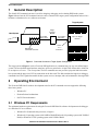
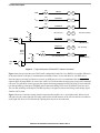
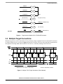
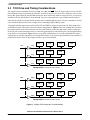
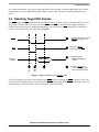
Freescale Semiconductor
Reference Manual
DSPCOMMPCIUM
Rev. 2, 3/2005
Suite56™ PCI Command Converter
User’s Manual
The Freescale Suite56™ PCI command converter is an interface
device that, with the assistance of the Suite56 DSP software
development tools debugger, allows you to send and receive
information from your host system to a DSP-based system. The
interface extends from the PCI bus on the host system through a
target interface module to the DSP via a JTAG connection. This
manual describes the operating environment and the
functionality of the PCI command converter.
© Freescale Semiconductor, Inc., 1999, 2005. All rights reserved.
CONTENTS
1
2
2.1
2.2
2.3
3
3.1
3.2
3.3
3.4
General Description ................................................ 2
Operating Environment........................................... 2
Windows PC Requirements .................................... 3
Hewlett Packard Workstation Requirements .......... 3
Sun Ultra Workstation Requirements .....................3
Functional Description............................................ 3
Command Converter Interface Connector .............. 4
Multiple Target Connections .................................. 5
TCK Drive and Timing Considerations .................. 6
Resetting Target DSP Devices................................ 7
General Description
1
General Description
The Suite56 PCI command converter is used for designing, debugging, and evaluating DSP-based systems.
Figure 1 shows how the PCI command converter can be connected in a target system configuration and used as a
hardware evaluation tool or as a software accelerator.
Target System
Target
Interface
Module
Host System
25-Pin OCD
Ribbon Cable
Suite56 PCI
Command Converter
14-Pin Ribbon
JTAG Cable
Up to 24 Target
Devices
14-Pin
2× 7
Connector
Figure 1. Command Converter to Target System Configuration
The target system in Figure 1 can be a Freescale DSP application or evaluation board, or any user-defined target
system. The user-defined target hardware must have an access point for the 14-pin JTAG ribbon cable, which can
be as simple as a 2-row × 7-set of test points. The PCI command converter provides a physical link between the
host system and the target via a PCI bus connection on the host card. This link translates the high-level debugger
commands into JTAG signals that enable the host system to reset, interrupt, and send commands to the target DSP.
2
Operating Environment
The Freescale DSP Suite56 software development tools for the PCI command converter support the following
three host systems:
•
Windows PC
•
Hewlett Packard workstations
•
Sun™ Ultra workstations
2.1 Windows PC Requirements
The minimum hardware requirements for using the Freescale DSP Suite56 software development tools debugger
on a Windows PC are as follows:
•
Windows PC (Pentium® class processor, or higher)
•
Windows® 95 operating system with 16 MB of RAM, Windows® 98 operating system with 32 MB of
RAM, or Windows NT 4.0 operating system with 32 MB of RAM
Suite56™ PCI Command Converter User’s Manual, Rev. 2
2
Freescale Semiconductor
Functional Description
•
CD-ROM drive
•
Mouse and keyboard
•
Hard drive with 50 MB of free space
•
Free PCI bus slot
2.2 Hewlett Packard Workstation Requirements
The minimum hardware requirements for using the Freescale DSP Suite56 software development tools debugger
on an HP Workstation include the following:
•
HP workstation running HP-UX version 9.05 or 10.20 (or higher)
•
32 MB of RAM
•
CD-ROM drive
•
Hard drive with 50 MB of free space
•
Mouse and keyboard
•
Free PCI bus slot
2.3 Sun Ultra Workstation Requirements
The minimum hardware requirements for using the Freescale DSP Suite56 Software Development Tools Debugger
on a Sun Ultra Workstation include the following:
3
•
Solaris™ Release 2.5.1 (or higher)
•
32 MB of RAM
•
CD-ROM drive
•
Hard drive with 50 MB of free space
•
Mouse and keyboard
•
Free PCI bus slot
Functional Description
The Suite56 PCI command converter interacts with the target DSP with the assistance of the Suite56 software
development tools debugger and the user’s host system. The host system interface consists of a C program that
sends commands via a PCI bus to the Suite56 PCI command converter. Commands entered from the host system
keyboard are parsed, and a series of low-level command packets are sent to the PCI command converter. The PCI
command converter translates these low-level command packets into one or more JTAG signals and OnCE
commands that are transferred to the target DSP via its JTAG port. The JTAG port provides the necessary control to
the target so programs can be loaded or saved, registers read or modified, and hardware breakpoints set or cleared.
3.1 Command Converter Interface Connector
The target application board must have a 14-pin connector to interface to the command converter controller. This
interface comprises eight signals and three ground connections on a 7-row × 2-column male pin header, which are
spaced on one-tenth inch centers as illustrated in Figure 2.
Suite56™ PCI Command Converter User’s Manual, Rev. 2
Freescale Semiconductor
3
Functional Description
10K
TDI/DSI
GND
1
2
3
4
5
6
7
8
9
10
10K
TDO/DSO
VCC
10K
TCK/DSCK
GND
VCC
(No Connect)
GND
Key (No Connect)
10K
CC_RESET
DSP RESET
Pin
TMS0 (For
JTAG Devices)
Target VDD
Target
Reset
Circuit
10K
VCC
VCC
11
12
13
14
(No Connect)
DEZ
(For JTAG Devices)
10K
TRST (For
JTAG Devices)
DSP TRST
Pin
Figure 2. Target VDD System JTAG/OnCE™ Interface Connector
Figure 2 may not represent the exact JTAG/OnCE configuration needed for every DSP due to possible differences
in internal resistors on the pins. For information on internal resistors, see the data sheet for your DSP device.
Since the target system has a resident reset circuit, an AND gate-in-series is recommended with the CC_RESET
signal to allow the target DSP to be reset with a valid VOL level from either the target-reset circuit or the command
converter. The pull-down resistors prevent false signals from being propagated to the JTAG/OnCE circuit when the
test data input/debug serial input (TDI/DSI) and test data clock/debug serial clock (TCK/DSCK) lines are active.
The test data out/debug serial output (TDO/DSO) pull-up is designed to deassert the Debug Acknowledge signal
from the OnCE circuit.
Figure 3 shows the connector coming from the target interface module via a 14-pin ribbon cable. When viewed
with pin 8 (keyed) on the right side, this plug connector has all odd numbers on the left side and all even numbers
on the right side when viewed from the top. Spacing between pins is one-tenth inch.
Suite56™ PCI Command Converter User’s Manual, Rev. 2
4
Freescale Semiconductor
Functional Description
.
TDI/DSI
TDO/DSO
TCK/DSCK
(No Connect)
CC_RESET
Target VDD
DEZ
Top View
1
2
3
4
5
6
7
8
9
10
11
12
13
14
GND
Key (No Connect)
TMS0 (For JTAG Devices)
(No Connect)
TRST (For JTAG Devices)
(For JTAG OnCE Devices)
Figure 3. Target Interface Module 4-Pin JTAG/OnCE Connector
3.2 Multiple Target Connections
Multiple target devices can be connected in a series, allowing a single command converter, JTAG/OnCE connector
to control multiple devices, as shown in Figure 4. Data flows from the JTAG host into each JTAG implementation
through TDI, out through TDO, and into TDI in the next device, eventually returning to the JTAG host.
RESET
TRST
TDO
TRST RESET
TRST RESET
TRST RESET
TRST RESET
TRST RESET
TRST RESET
TDI
TDO
TDI
TDO
TDI
TDO
TDI
TDO
TDI
TDO
TDI
TDO
TCK
TMS
TCK
TMS
TCK
TMS
TCK
TMS
TCK
TMS
TCK
TMS
TDI
TCK
TMS
Maximum of Four Loads on TCK Circuits
Buffer is 74HCT244 or Similar
Figure 4. Multiple JTAG Target Connections (Serial Method)
Suite56™ PCI Command Converter User’s Manual, Rev. 2
Freescale Semiconductor
5
Functional Description
3.3 TCK Drive and Timing Considerations
The signals from the command converter are TDO, TCK, TMS, and TRST. The TCK signal requires fast rise and fall
times dictated by the TCK pin timing specification, so attention must be given to the drive capability of the circuits
driving this signal. When the TCK and TMS circuits are driven with a large number of target devices, you must pay
attention to the rise and fall times of TCK and TMS. Excessive capacitance may cause communication problems
when driving a single circuit that connects multiple TCK or multiple TMS input pins. Excessive capacitance can also
cause communication problems with a single circuit connecting multiple TMS input pins.
Acceptable transition times may be achieved for TCK and TMS by driving no more than four JTAG inputs from
each buffered output. This may be achieved with two configurations. Figure 4 shows one method. Here (in effect)
one signal connects each of the TCK inputs, and one signal connects each of the TMS inputs. A buffer is placed in
the circuit after each fourth input at most, to restore the signal quality for subsequent inputs. The propagation delay
of the buffer is not significant. Figure 5 shows two possible configurations of a second method that also enables
signal quality to meet the requirements. In configuration Number 1, the signal is split and buffered into a number of
parallel TCKx signals. Each of these signals can drive up to four TCK inputs.
TCK
TCK
TCK
TCK
TCK
TCK
TCK
TCK
TCK
TCK
TCK
TCK1
TCK2
TCK
TCKn
Configuration 1: Fan Out of TCK at Source
TMS
TMS
TMS
TMS
TMS
TMS
TMS
TMS
TMS
TMS
TMS
TMS1
TMS2
TMS
TMSn
Configuration 2: Fan Out of TMS at Source
Figure 5. Multiple JTAG Connectors (Parallel Method)
Suite56™ PCI Command Converter User’s Manual, Rev. 2
6
Freescale Semiconductor
Functional Description
In Configuration Number 2, the signal is split and buffered into a number of parallel TMSx signals. Each of these
signals can drive up to four TMS inputs.Each method is equally valid. The choice of methods depends on the
project.
3.4 Resetting Target DSP Devices
The RESET signal and TRST signals from the command converter typically connect to all target DSP devices on a
JTAG chain. All these DSP devices are reset when RESET and TRST are asserted by the debugger command
FORCE R. Execution control is established immediately after deassertion of TRST and before any instructions
execute. This sequence of events is illustrated in Figure 6.
(1) Command converter asserts
RESET. All targets enter
reset.
RESET
(2) Asserted TRST.
(2A) Deasserted TRST.
TRST
DEBUG_REQ
Instruction
Register
(1)
(2)
(2A)
(3)
(4)
(3) JTAG instruction
DEBUG_REQUEST is
loaded.
(4) Command converter
releases RESET. Targets
exit reset in Debug mode.
Figure 6. Reset JTAG Device with RESET Signal
The JTAG controller is still active after deassertion of TRST during reset and while RESET is held low. The JTAG
special instruction DEBUG_REQ is clocked in before RESET is deasserted. When RESET is deasserted, the device
immediately goes into Debug mode, and no instructions execute in the DSP.
Suite56™ PCI Command Converter User’s Manual, Rev. 2
Freescale Semiconductor
7
How to Reach Us:
Home Page:
www.freescale.com
E-mail:
[email protected]
USA/Europe or Locations not listed:
Freescale Semiconductor
Technical Information Center, CH370
1300 N. Alma School Road
Chandler, Arizona 85224
+1-800-521-6274 or +1-480-768-2130
[email protected]
Europe, Middle East, and Africa:
Freescale Halbleiter Deutschland GMBH
Technical Information Center
Schatzbogen 7
81829 München, Germany
+44 1296 380 456 (English)
+46 8 52200080 (English)
+49 89 92103 559 (German)
+33 1 69 35 48 48 (French)
[email protected]
Japan:
Freescale Semiconductor Japan Ltd.
Headquarters
ARCO Tower 15F
1-8-1, Shimo-Meguro, Meguro-ku,
Tokyo 153-0064, Japan
0120 191014 or +81 3 5437 9125
[email protected]
Asia/Pacific:
Freescale Semiconductor Hong Kong Ltd.
Technical Information Center
2 Dai King Street
Tai Po Industrial Estate
Tai Po, N.T. Hong Kong
+800 2666 8080
For Literature Requests Only:
Freescale Semiconductor Literature Distribution Center
P.O. Box 5405
Denver, Colorado 80217
1-800-441-2447 or 303-675-2140
Fax: 303-675-2150
[email protected]
Document
Order
DSPCOMMPCIUM
Rev. 2
No.:
Information in this document is provided solely to enable system and software implementers to
use Freescale Semiconductor products. There are no express or implied copyright licenses
granted hereunder to design or fabricate any integrated circuits or integrated circuits based on
the information in this document.
Freescale Semiconductor reserves the right to make changes without further notice to any
products herein. Freescale Semiconductor makes no warranty, representation or guarantee
regarding the suitability of its products for any particular purpose, nor does Freescale
Semiconductor assume any liability arising out of the application or use of any product or
circuit, and specifically disclaims any and all liability, including without limitation consequential
or incidental damages. “Typical” parameters which may be provided in Freescale
Semiconductor data sheets and/or specifications can and do vary in different applications and
actual performance may vary over time. All operating parameters, including “Typicals” must be
validated for each customer application by customer’s technical experts. Freescale
Semiconductor does not convey any license under its patent rights nor the rights of others.
Freescale Semiconductor products are not designed, intended, or authorized for use as
components in systems intended for surgical implant into the body, or other applications
intended to support or sustain life, or for any other application in which the failure of the
Freescale Semiconductor product could create a situation where personal injury or death may
occur. Should Buyer purchase or use Freescale Semiconductor products for any such
unintended or unauthorized application, Buyer shall indemnify and hold Freescale
Semiconductor and its officers, employees, subsidiaries, affiliates, and distributors harmless
against all claims, costs, damages, and expenses, and reasonable attorney fees arising out of,
directly or indirectly, any claim of personal injury or death associated with such unintended or
unauthorized use, even if such claim alleges that Freescale Semiconductor was negligent
regarding the design or manufacture of the part.
Freescale, the Freescale logo, OnCE, and Suite56 are trademarks of Freescale
Semiconductor, Inc. All other product or service names are the property of their respective
owners.
© Freescale Semiconductor, Inc. 1998, 2005.