1
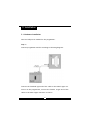
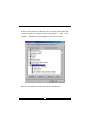
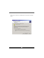
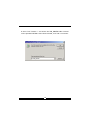
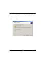
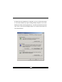
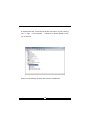
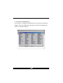
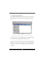
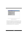
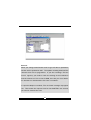
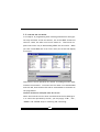
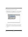
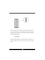
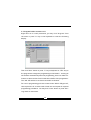
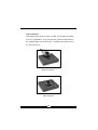
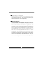
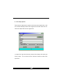
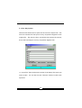
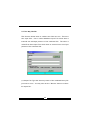
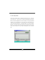
ALL-11A User’s Manual
Aug, 2005
© 2005 HI-LO SYSTEM RESEARCH CO., LTD.
(http://www.hi-lo.com.tw)
Information provided in this document is proprietary to HI-LO System Research Co., Ltd.
The information in this publication is believed to be accurate in all respects at the time of
publication, but is subjejct to change without notice.
HI-LO assumes no responsibility for nay errors or omissions, and disclaims responsibility
for any consequence resulting from the use of the information included herein.
Trademarks
HI-LO is a trademark of HI-LO System Research Co., Ltd.
AMD is a trademark of Advanced Micro Devices, Inc.
Windows 95/98/Me/NT/2000/XP/2003 are trademarks of Microsoft Corporation.
IBM is a trademark of IBM Corporation.
All other trademarks are the property of their respective owners.
Contents
1. Intruduction ..................................................... 1
1.1 Programmer and accessories ....................................1
1.2 PC System Requirements ........................................ 2
2. Installation ....................................................... 3
2.1 Hardware Installation ............................................ 3
2.2 USB driver Installation ........................................... 5
2.3 Software Installation ............................................. 20
3. Utilization ........................................................ 27
3.1 Starting the system .............................................. 27
3.2 Load disk file into buffer ........................................ 32
3.3 Read contents from master IC to buffer ....................... 33
3.4 Insert a blank IC into the socket ............................... 35
3.5 Program buffer contents to IC .................................. 36
3.6 Expansion adapter and converter .............................. 37
4. Glossary ........................................................... 39
4.1 EPROM, EEPROM, PROM and MPU ............................ 39
4.2 PLD, PAL, GAL, PEEL, CPLD, EPLD and FPGA ............. 44
5. Utilities ............................................................ 47
5.1 Hex File converter — Hex to Binary file converter ........... 48
5.2 Bin to Hex converter — Binary to Hex file converter ......... 50
5.3 Two-Way Splitter ................................................. 52
5.4 Four-Way Splitter .................................................54
5.5 Two-Way Shuffler ................................................. 56
5.6 Four-Way Shuffler ................................................ 58
6. Job Function .................................................... 60
7. Serial Number Function (Serialization) .................63
Appendix ............................................................. 66
1. Intruduction
ALL-11A, the programmer, works with IBM PC through USB (Universal
Serial Bus) port to perform a high-speed data transmission and accurate
programming waves. ALL-11A is embeded with a 1Mbit memory to support the programming capacity for most E(E)PROM、MCU/MPU and PLD.
The software automatically uses PC memory If the buffer for the device
is over 1 Mbit. This manual contains how to install the system and work
under environment of IBM PC Windows 98/Me/2000/XP/2003.
1.1 Programmer and accessories
Each ALL-11A package contains following items:
ALL-11A programmer.
An AC power cable, 1.8 M.
A USB signal cable converting A type to B type; 1 meter long.
A CD-ROM for Driver Files.
User’s manual
1
1.2 PC System Requirements
PC/Pentium above
Microsoft compatible mouse
A harddisk with at least 20 Mbyte usable capacity
A CD-ROM drive
1 USB port for programmer
Operating system: Windows 98/Me/2000/XP/2003
2
2. Installation
2.1 Hardware Installation
One free USB port is needed for the programmer.
Step 1:
Connect programmer and PC according to follwoing diagram:
Connect the female B type end of the cable to the male B type connector on the programmer, connect the female A type end of the
cable to the male A type connector on the PC.
3
Step 2:
Connect one end of the power cable to programmer(socket is next to
switch of the programmer), the other end to the outlet of power
source. Switch on PC first, then the programmer. Once the programmer is on, signals on LED should show as follows:
ON LED - lit
Busy LED - off
Good LED - off
If LEDs do not lit as above mentioned, you need to do the first check
by turning off PC and programmer, then check connections between
programmer and USB port. Later, turn on PC and progrmmer a second time to check the LED again. If error message remains, other
hardware peripherals may have conflict with the I/O address you are
applying now.
4
2.2 USB driver Installation
After connecting your PC and programmer with the USB cable, switch
the programmer on. The PC will detect the new hardware and a
window will open showing “Add New Hardware Wizard” with the
name HiLo Systems --- USB Drivers. To install the USB driver with
Windows 98/Me, please refer to the procedures from 2.2.1 to 2.2.7.
For Windows 2000/XP/2003 please refer to the procedures from 2.2.8
to 2.2.15.
2.2.1 Click “Next” to continue.
5
2.2.2 Click on “Search for the best driver” and then “Next”.
6
2.2.3 Click “Browse..” and select the USB_DRIVER folder located on
the provided CD-ROM. After this is selected, click “Next” to continue.
7
2.2.4 Windows should automatically select “FTD2XX.INF”. Click
“Next” to continue.
8
2.2.5 Click “Finish” to complete the USB driver installation.
9
2.2.6 Once the installation is complete, you can confirm the status
of the new hardware by right clicking the My Computer icon on the
desktop and then selecting Properties.
10
2.2.7 Choose the Device Manager tab on the top and expand the
Universal serial bus controller by left clicking the “+” sign. “HiLo
Systems--- USB Drivers” should appear in the list of devices.
Return to the desktop to start the software installation.
11
2.2.8 (For Windows 2000/XP/2003)
Click “Next” to continue.
12
2.2.9 Click on “Search for a suitable driver for my device” and then
“Next”.
13
2.2.10 Choose “Specify a location” and then Click “Next” to continue.
14
2.2.11 Click “Browse..” and select the USB_DRIVER folder located
on the provided CD-ROM. After this is selected, click “OK” to continue.
15
2.2.12 Windows should automatically select “FTD2XX.INF”. Click
“Next” to continue.
16
2.2.13 Click “Finish” to complete the USB driver installation.
17
2.2.14 Once the installation is complete, you can confirm the status
of the new hardware by right clicking the My Computer icon on the
desktop and then selecting Properties. Choose the Hardware tab and
then click on the Device Manager Button to confirm the presence of
the new hardware.
18
2.2.15 Expand the “Universal Serial Bus controllers” by left clicking
the “+” sign. “ HiLo Systems --- USB Drivers” should appear in the
list of devices.
Return to the desktop to start the software installation.
19
2.3 Software Installation
Insert the CD-ROM to your CD-ROM drive, go to directory of ALL-11A
under File Manager to execute the SETUP.EXE file, or activate the
SETUP.EXE from START menu of WINDOWS and follow all steps accordingly as follows:
20
Cautions and Descriptions:
1. Log in with “Administrator” to install the S/W if under Windows
2000/XP/2003.
2. Apply File Manger to check the completion of S/W installation
over WACCESS.EXE, individual driver file and other utilities.
WACCESS.EXE is a main system file that provides fairly easy way
to select IC manufacturer, type and special driver file needed.
Each single driver file can also be run separately from WACCESS.
EXE rule. A programming file usually support a series of relevant
ICs. For instance, WMEM1.EXE is able to program 2716 to 27C512
EPROM.
3. An automatic self-check over the programmer will work either a
driver file or the option function of WACCESS.EXE is executed.
If message shows programmer does not exist, stop all your
operation and check your installation again.
4. Two alternatives to check the existence of the programmer:
Method 1: Execute “Option” function under WACCESS menu
Method 2: Execute selected driver file under WACCESS menu
21
Method 1
Method 2
WACCESS
WACCESS
(ACCESS file)
Main Menu
Main Menu
Option
DEVICE
I/O Base Address
WPLD1.EXE
(Driver File)
EXIT
DEVICE Driver File
Main Menu
I/O Base Address
EXIT
Method 1: Execute “Option” function under WACCESS menu
Select “WACCESS” under File Manager or press “Start” and “program
files” then click “Programmer” to evoke the following display.
22
Click “I/O Base Address” under “Option” to evoke the following
display:
23
The I/O Base Address set for current S/W will show on the screen, the
system will then check the existance of programmer automatically.
When “Programmer Status: Exist” appears, the H/W installation is
completed.
When “Programmer Status:Not Exist” message appears, the failure could be caused by following 5 reasons:
1. I/O Base Address conflict between S/W and H/W.
2. IRQ setting of I/O port conflicts with other cards added on PC.
3. Poor connections between cable and interface card.
4. Programmer is powered off.
5. The USB driver is not installed correctly.
Following Steps will guide you to find the fact.
1. Make sure the green LED must be lit when powered on.
2. Check if cable firmly connected between programmer and USB
port of the PC.
3. If the USB port setting is not working, please ensure the PC’s
BIOS setup has USB Controller enabled.
Remark:
When exit the programming program, I/O address will be saved for
future utilization.
24
Method 2: Execute selected driver file under WACCESS menu
When manufacturer and type info are entered for each IC, the driving
file will be automatically called by WACCESS. You can also execute
the driver file without through WACCESS.
Take WPLD1, a file for programming GAL, as an example. When
WPLD1.EXE is executed, it will search for WPLD1.DAT first. If the
file is in the default disk, all its parameters including I/O Base Address,
manufacturer, type will be loaded as default value. If not, then
COM2, AMD(manufacturer), PALCE16V8H(type) will be taken as default value.
Execution of a driver file is H/W checking inclusive. When all checks
are passed, the system is ready for programming and the main menu
will appear as follows:
25
When an error message as above appears, you need to consider following 3 reasons:
1. IRQ conflict between USB port and additional PC card
2. The programmer is switched off
3. You have to make sure the PC’s BIOS setup has USB controller
enabled.
When the error remains after checking, you may apply the following
solutions:
1. Back to programming main menu by pressing OK key, then select “I/O SETUP” via “SETUP” menu, select “USB” and check
the “Programmer Status: Exist” appears.
2. When the first solution fails, you may exit the menu by pressing
“Q”, then check if any conflict between IRQ setting and other
PC peripherals. If yes, reselect IRQ.
3. When above both ways fail, please contact your local dealer.
26
3. Utilization
3.1 Starting the system
A brief introduction about how to enter WACCESS, the main program,
and proceed other relavent functions like Device selection, Data
loading, blank check and programming etc. will be presented below
PALCE16V8 as an example.
3.1.1 Begin with WACCESS
Click the icon of WACCESS to activate WACCESS.EXE and get following display on the window.
27
3.1.2 Select the manufacturer
Click “Device” to display all manufacturers for selection as following
display. Then click “AMD” adn press OK key to get the next display with
menu of IC groups and types.
28
3.1.3 Select the IC group and type
For this default example, you may click “PLD”, then search and click
on the desired type in the right side menu followed by clicking <Run>
key.
After the execution of <Run>, WACCESS file will automatically activate
all realted functions to get WPLD1.EXE ready for execution.
You may also run a specific driver file directly without going through
WACCESS. You can select all parameters in its main menu by first
click “Device” function, then followed by other selections as following diaplay.
29
Main Menu of the Driver File
The main menu of programming file contains three vital parts. From
top row down, you see the first row for main functions, the second
row for quick function keys, and the rest provide detailed programming parameters about the selected IC, that includes manufacturer,
type, ADAPTER required and current I/O Base Address etc.
30
Remark:
When you change manufacturer and IC type all data in parameter
window will be updated as well. The update including download the
relevant driver file to programmer. If you see a message “File not
found” appears, you need to check the missing of the installation
and the existence of file in the CD-ROM, then ask your local dealer
for assistance or download the file from our website.
If a specific adapter is needed, “File not found” message may appear
too. That means the required S/W for the ADAPTER is not existed,
you need to reinstall the S/W.
31
3.2 Load disk file into buffer
It is ready for IC programming after selecting manufacturer and type.
You may use either of the two sources, one is the JEDEC format file
saved in a disk, the other one from a master IC. This section explains the former way of downloading JEDEC file into buffer. When
you click “Load JEDEC file” from “File” menu, the screen will display
as follows:
This function and its operation are similar to loading function under
windows environment. You enter the file name to be downloaded
and click OK, then the data file will be transmitted to the buffer of
the programmer.
Caution: Disk driver and path must be correct
Select and click the correct driver and folder that the file belongs to.
If it cannot be operated by mouse, you may apply <TAB>, <UP>,
<DOWN> and <ENTER> keys for selecting and confirming.
32
3.3 Read contents from master IC to buffer
When data is stored in an IC instead of a disk, you may press “R” key
on the keyboard or click the “READ” button on screen to read data
from IC and transfer it to Buffer. The screen show as follows:
Release the socket lever, set IC in position, pin 1 of IC on the same
side as the lever, if IC has less pin numbers than the socket, the Pin
1 alignment is from the opposite side of the lever as following
diagram:
33
Press down socket lever to fasten the IC in position, then click “Run” on
screen or press down “Y” key of keyboard or press “YES” key on programmer to start the function. As the function is in process, the screen
will show following message.
Reading Now
When OK! message appears, the reading function is completed. You
may click “Close” button or press <ESC> key for returning to main
menu.
34
3.4 Insert a Blank IC into the socket
When programming data is read either from buffer or master IC, it is
ready for programming operation and you have to insert a blank IC in
position. Do follow correct IC positioning as stated on Section 3.3.
Press “B” key on keyboard before programming to blank check the
IC.
Attention!
Wrongly positioned IC may be damaged or be programmed to an unknown state.
35
3.5 Program buffer contents to IC
Right after an IC is well positioned, you may click “Program” from
the menu or press “P” key on the keyboard to evoke the following
display.
Then click “Run” button or press “Y” key on keyboard or “YES” key on
the programmer to begin the programming on the blank IC. A verify job
will be done automatically after the programming, that is to make verification on what read out from IC with that in buffer of the programmer.
The “OK” LED will be lit to show a successful verification.
For next IC programming you have to wait till the “BUSY” LED goes off,
then replace the IC in socket with a blank one and repeat all required
programming procedures. You may click “Close” button or press <ESC>
to go back to main menu.
36
3.6 Expansion ADAPTERs and CONVERTERs
Many more ADAPTERs and CONVERTERs were evolved according to
different IC types and packages like PLCC, SOP, TSOP, QFP, PGA, etc.
to meet the rapid development of programmable ICs.
ADAPTER:
Each ADAPTER comes with 40 pins that match the 40-pin socket
on the programmer. Each ADAPTER has one or more programming files that to be copied to the same directory as WACCESS.
CONVERTER:
CONVERTERs support the conversion from DIP package to others
like PLCC, SOP, TSOP etc. In application, no extra programming
file is needed because it is only a simple pin conversion.
3.6.1 ADAPTER and CONVERTER installation
S/W Installation:
As what stated under ADAPTER, the S/W need be copied through
the same directory as that for WACCESS file.
37
H/W Installation:
Like positioning a 40-pin IC onto a socket, you release the socket
lever on programmer, then proceed the insertion and fasten it
by pressing down the socket lever. Following two pictures are
for your reference.
Before insertion
After insertion
38
4. Glossary
4.1 EPROM, EEPROM, BPROM and MPU
Programmable DEVICE :
An integrated circuit (IC) that will be programmed or copied.
Bit, Nibble, Byte, Word and Double word :
Bit
: A basic unit of Binary data.
Nibble : A group of 4-bit Binary data.
A nibble's value ranges from 0H to FH.
Byte
: A group of 8-bit Binary data.
A byte's value ranges from 0H to FFH.
Word
: A group of 16-bit Binary data.
A word's value ranges from 0H to FFFFH.
Double Word : A group of 32-bit binary data.
A double word's value ranges from 0H to
FFFFFFFFH.
Working Buffer :
A block of memory inside the programmer allocated by the device
driver file. The working buffer is used by the device driver file as
an intermediate storage.
39
When you want to program a data file to a DEVICE, you first load the
file to the working buffer. The contents in the working buffer are
then programmed to the target DEVICE. When you read the contents of a master DEVICE, the data is stored in the working buffer,
that can then be edited or saved to disk for future reference.
Buffer Start and Buffer End Addresses:
The buffer start and end addresses are offset addresses specified from the base address of the Working Buffer. The data stored
between the buffer start and buffer end addresses contains the
sub-set of the programmer memory buffer is to be programmed
to a target
device. This is also the area of the buffer for
CheckSum calculations.
CheckSum:
This is the sum of all data contents between buffer start and end
addresses. All data are added byte by byte and then the least
significant 16 bits (4 HEX characters) are displayed as the
checksum. Some bytes in the address range may not be added to
the checksum as specified by the manufacturer of the particular
DEVICE. CheckSums will be calculated during DEVICE reading,
file loading, type changing or after buffer editing.
40
Bit count of the data:
NIBBLE width is 4.
BYTE width is 8.
WORD width is 16.
Double Word has a width of 32.
The bit count of MPU is usually 8 or 16, but is also available in 12,
14, or other counts as device type varies.
Device Start and Device End Addresses:
The DEVICE start and end addresses are offset addresses specified from the base address of the DEVICE. Data stored at the
buffer start address in the working buffer will be programmed to
a DEVICE beginning at the Device Start Address location.
NOTE :
In order to get correct programming data, some device files forbid users to change the address settings for Buffer Start, Buffer
End, Device Start, and Device End.
I/O Address :
This is the I/O port select for the USB port .
41
Security Fuses:
Security fuses are present in many programmable devices. When
a security fuse is programmed the data stored inside the device can
not be read out correctly for reverse engineering purposes. Generally a device will be read as blank if the security fuse is blown. The
device will operate functionally equivalent with the security fuse intact or blown.
Remark:
Please check with your data book before programming the security fuse of a UV erasable(windowed) device because some UV
erasable devices can not be programmed again once the security
fuse is programmed.
Lock Bits:
Some microcontrollers use lock bits in place of a single security
fuse. Usually you have the option of selecting to program one
lock bit or all lock bits to provide different levels of code
protection. The definition of these bits varies from manufacturer to manufacturer. Please consult the data book of your target device for more details. For some devices like Microchip PIC
series devices, if the Lock Bits in the data file are set, the
checksum will be different.
42
Encryption:
Some MCU/MPU are encrypted for protection. For a programmed IC
that has been encrypted, a correct decrytion code must be given in
order to read correct data.
Protection Fuses:
Some FLASH based memory devices have protection fuses. A
Protection fuse is used to protect a sector of memory in the
FLASH
device from being accidentally programmed or modified
by the target hardware where the device will be installed. This
fuse must be reset by a specific series of procedures before the
data in the particular sector can be programmed or changed to
new values. Protection fuses are only programmed using the
separate "Protection" function or the "Auto" function.
43
4.2 PLD, PAL, GAL, PEEL, CPLD, EPLD and FPGA
Programmable Logic Device (PLD):
Generally speaking, a device that can be programmed to perform
many different logic operations is a PLD. PLDs are usually grouped
into following five categories:
PLD
: A one time programmable logic device such as a PAL
device.
EPLD : A UV erasable PLD such as a EPLD, CPLD, or FPGA
device. These devices contain a transparent window on
top for UV light exposure.
EEPLD : An electrically erasable PLD such as a GAL, PEEL, CPLD,
or FPGA device.
CPLD : A more complex PLD device.
FPGA : Field programmable gate array.
JEDEC Fuse Map File of a PLD Device:
The JEDEC fuse map file is the standard format which can be
loaded to a programmer for programming PLD's. It contains fuse
information(Blown/Intact) and the Function Test Vectors of the
PLD(optional). Most PLD assemblers or compilers, such as the
PALASM, OPAL, CUPL, ABEL, AMAZE and PDK-1, can produce a
JEDEC fuse map file.
44
POF fuse map file for PLD devices:
The POF fuse map file is a format used for programmable logic devices from Altera Corporation. POF files store programming fuse
data for larger devices in a more compact way.
Fuse Blown and Intact:
A new programmable device generally comes with all fuses in an
intact state (i.e. logic 1 or blank state). The designer can only
blow an Intact fuse into a Blown state i.e. logic 0 state. The
initial state of some devices may be opposite to this depending
upon the device manufacturing method. For those one time
programmable(OTP) devices you cannot change the state of a
fuse back to the unprogrammed state once it is blown
(programmed). UV erasable devices come with windows. When
the window is exposed to UV light long enough the fuses will be
erased to its initial blank(or unprogrammed) state. Other devices are electrically erasable and can be erased by using an ERASE
function on the Programmer.
45
Array Fuses & Configuration Fuses:
Array fuses are the main logic fuses in a PLD. Different arrangements(Blown/Intact) have different logic functions. Configura-tion
fuses indicate the I/O architecture of the PLD, such as Combinatorial/Registered, Output Feedback/Output Enable. Generally,
the user do not have to know the exact details of these fuses
because the logic compiler used to translate your logic statements
and equations into a JEDEC fuse map or another format
for programming into a device will specify the value of these
bits.
Security Fuses
Security fuses are present in many PLD devices. When the security fuse is programmed the data stored inside the PLD can not be
read out correctly for reverse engineering purposes. Generally a
device will be read as blank if the security fuse is blown. The
device will carry on all functions and disregard the security fuse
is intact or blown.
46
5. Utilities
Some functions such as Hex to Binary file converter, Binary to Hex
File converter, etc. are provided in the Utility function. They are
described as follows:
47
5.1 Hex File converter — Hex to Binary file converter
(1) Input Hex File: Type the directory/name of your HEX format file
which you want to convert to a Binary file. You can also use the
“Browse” button to select the input file.
(2) Output Bin File: Type the directory/name of your output binary
file converted from the HEX file and have it saved.
(3) File Format: Select the desired HEX format. You can choose from
Intel HEX 16, Intel HEX 32, Motorola HEX, etc.
(4) Start Address: Type the beginning address of the HEX file you
want to convert.
48
(5) End Address: Type the end address of the HEX file you want to
convert.
(6) Unused Byte: Some HEX format files may not have consecutive
data so you will need to select the unused data (00H or FFH) to fill in
the inconsecutive area when you convert the file to Binary format.
49
5.2 Bin to Hex converter — Binary to Hex file converter
(1) Input BIN File: Type the directory/name of your binary file which
you want to convert to a HEX file. You can also use the “Browse”
button to select the input file.
(2) Output HEX File: Type the directory/name of your output HEX file
converted from the BIN file and have it saved.
(3) File Format: Select the desired HEX format. You can choose from
Intel HEX 16, Intel HEX 32, Motorola S1, Motorola S2, and Motorola
S3.
50
(4) Input BIN File Start Address: Type the beginning address of the
BIN file you want to convert.
(5) Output HEX File Start Address: Type the beginning address of the
HEX file to be converterd from the BIN file.
51
5.3 Two-Way Splitter
This function allows users to split one file into two output files. One
file contains odd-byte data of the original file and the other file contains even-byte data of the original file.
(1) Input File: Type the directory/name of the binary file which you
want to split. You can also use the “Browse” button to select the
Input File.
52
(2) Output File:
a. Even: Type the directory/name of the splited Even Data
Output File you want to save.
b. Odd: Type the directory/name of the splited Odd Data Output
File you want to save.
(3) Split Data Format: Normally the split data is in Byte Wide mode.
That means define one byte wide as unit of data split. However
users can choose Word Wide (two bytes) or Double Word Wide (four
bytes) as unit of data split.
53
5.4 Four-Way Splitter
This function allows users to split one file into four output files. The
first file contains the first byte of every 4-byte data segment of the
original file. The second, third, and fourth files contain the second,
third, and fourth bytes of every 4-byte data segment file.
(1) Input File: Type the directory/name of the binary file which you
want to split. You can also use the “Browse” button to select the
input file.
54
(2) Output File:
a. 1st: Type the directory/name of the First-Byte Output Data
File you want to save.
b. 2nd: Type the directory/name of the Second-Byte Output Data
File you want to save.
c. 3rd: Type the directory/name of the Third-Byte Output Data
File you want to save.
d. 4th: Type the directory/name of the Fourth-Byte Output Data
File you want to save.
(3) Split Data Format: Normally the split data is in Byte Wide mode.
That means define one byte wide as unit of data split. However
users can choose Word Wide (two bytes) or Double Word Wide (four
bytes) as unit of data split.
55
5.5 Two-Way Shuffler
This function allows users to combine two files into one. There are
two input files. One is called Odd Data Input File which data is
inserted into odd byte position of the combined file. The other is
called Even Data Input File which data is inserted into even byte
position of the combined file.
(1) Output File: Type the directory/name of the combined binary file
you want to save. You may also use the “Browse” button to select
an output file.
56
(2) Input File:
a. Even: Type the directory/name of the Even Data Input File you
want to be combined.
b. Odd: Type the directory/name of the Odd Data Input File you
want to be combined.
(3) Shuffle Data Format: Normally the shuffled data is in Byte Wide
mode. That means define one byte wide as unit of data shuffle.
However users can choose Word Wide (two bytes) or Double Word
Wide (four bytes) as unit of data shuffle.
57
5.6 Four-Way Shuffler
This function allows users to combine four files into one. There are
four input files. The first file is called First-Byte Data File which
data is inserted intoposition of the first byte of every 4-byte data
segment in the combined file. The second, third, and fourth file is
called Second-Byte Data File, Third-Byte Data File, and Fourth-Byte
Data File. Their data respectively inserted into positions of the second,
third, and fourth byte of every 4-byte data segment in the combined
file.
58
(1) Output File: Type the directory/name of the combined binary file
which you want to save. You may also use the “Browse” button to
select an output file.
(2) Input File:
a. 1st: Type the directory/name of the First-Byte Data File
you want to combine.
b. 2nd: Type the directory/name of the Second-Byte Data File
you want to combine.
c. 3rd: Type the directory/name of the Third-Byte Data File
you want to combine.
d. 4th: Type the directory/name of the Fourth-Byte Data File
you want to combine.
(3) Shuffle Data Format: Normally the shuffled data is in Byte Wide
mode. That means define one byte wide as unit of data shuffle.
However users can choose Word Wide (two bytes) or Double Word
Wide (four bytes) as unit of data shuffle.
59
6. Job Function
The Programmer driver contains three special functions under the
“File” dropdown menu; Load Programmer Configuration, Save Programmer Configuration, and Enable Job Function.
a) Save Programmer Configuration
This feature allows you to save all settings selected in the software
driver, including:
1. Mfr. & Type selections
2. Load File setting
3. Target Zone settings including Device Start, Device End, Buffer
Start, & Buffer End
4. Other programming settings
5. Auto function settings
After all settings have been entered indluding Auto Function section,
select the Save Programmer Configuration under the “File” dropdown
menu and type the filename you want to save.
b) Load Programmer Configuration
After saving the configuration information settings using the Save
Programmer Configuration command, you may then use the Load Programmer Configuration to load the desired configuration into the
software driver. You select the Load Programmer Configuration under the “File” dropdown menu and then choose the filename of the
60
configuration data you want to use. The software will automatically
load the programming data (note: not all software contains Target
Zone data).
The “Auto” function will also reinstall all the settings used for the
previously programmed device. After completing data entry to the
Load Programmer Configuration window, users only need to select
the “Auto” function to begin programming.
c) Enable Job Function
This function allows users to enable or disable Job Function. After
clicking the Enable Job Function block to have it enabled, a check
mark appears by its side, any previously saved programmer configuration can be easily installed. The next time the program software
driver is executed, a file selection window will automatically appear
so that you can select the programmer configuration file you want to
use. This function will then automatically open the Auto function
window for your convenience. Users may also install a short cut to
the programmer driver software in the Startup directory of Windows
so that the driver will automatically start when your PC is turned on
and Windows is started.
61
62
7. Serial Number Function (Serialization)
When using the Serial Number function on the ALL-11A, you must be
aware of its functions and limitations, which are as follows:
1. Press S/N Setup button in the “AUTO” window to setup the Serial
Number function
2. Serial Number On/Off:
This function can be selected to enable or disable the Serial Number
function (The Serial Number function is only available in the “AUTO”
mode.)
3. Length:
This function sets the length of the serial number. It can be up to 8
bytes (16 digits) long.
4. Display Format:
This function selects the display format of the serial number, either
HEX (Hexadecimal) or BCD (Binary Coded Decimal).
5. S/N Start Address:
This function is used to set the starting memory address for serial
number programming.
63
6. Start Serial No.:
This function is used to set the starting value of the serial number.
7. Direction:
This function is used to specify the sorting order of the serial numbers either from low to high (Low Byte) or high to low (High Byte).
8. After programming the data, the serial number will automatically
increase by one for next programming.
9. Not all the programmer software can use the Serial Number function (ex: PLD software can not support this function.)
10. The serial number setting for Microchip PIC series devices is
different from other devices. Its high byte data of serial number
locations is fixed (12 Bits device is 08H. 14 Bits device is 37H, 16
Bits device is B6H).
For example, if the user selected serial number is “1234ABCD”
then data will be programmed from the beginning of the serial number start address and its data will be formed as follows:
Programmed data to PIC16C54 (12 Bits) is 0812H 0834H 08ABH 08CDH
Programmed data to PIC16C62 (14 Bits) is 3712H 3734H 37ABH 37CDH
Programmed data to PIC17C42 (16 Bits) is B612H B634H B6ABH B6CDH
64
11. The following is an example of the Serial Number Function:
65
Appendix
Troubleshooting
For problems with individual functions please refer to the specific
function description under the Function Reference Guide.
Problem 1
When I try to run a driver file, I get communication error messages.
Resolution
1-1 You may not have the USB port set correctly for your programmer.
Double check the I/O port assignment.
1-2 There may be a bad connection between the USB port due to a
faulty cable. Double check the cable connection.
1-3 You must set the USB controller enabled in your PC’s BIOS setup.
Problem 2
You have more than two programming failures in a programming cycle.
Resolution
2-1 Check if these devices are inserted in the ZIF socket correctly.
2-2 Check with your distributor to make sure you have the latest
version of file.
66
Problem 3
My operating system is Windows 2000/XP/2003. I can not install the
programmer with the USB port.
Resolution
Please note when you install the software in Windows 2000/XP/2003 or
above, you must be logged on as an Administrator first.
67
Eight things to do Before Calling Your Dealer:
1.
Reboot the computer and try again.
2.
Repeat all the steps, following the instructions in this manual.
3.
Close all other programs running under windows.
4.
See if your problem is listed in the Trouble-Shooting section.
5.
Try it on another system.
6.
Compare system requirements with your configuration.
7.
Ask your in-house specialist (every office has one).
8.
Consult the person who installed the product if available.
68
General Troubleshooting Checklist
If your problem is not as such described above, check the followings:
1. Is the USB port interface card fully seated in its slot?
2. Are all cable connections securely fastened?
3. Is the setting on the USB port correct?
Web Support
If you wish to get updated software, please download the EXE and
WPROG.DEV files from our web site, http://www.hilosystems.com.
tw. You then have to copy them to the desired directory.
69