1
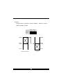
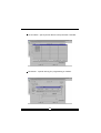
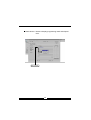
ALL-100 /P/G/G4
Universal & Gang Programmer
User’s Manual
Aug. 2007
Caution : USB Interface Compatibility
For USB 2.0 compatibility, the revision of your computer
operation system should be no earlier than following editions :
Windows 98 SE/Me/2000 SP4/XP SP1/Server 2003/Vista
Software incompatible may happen if your computer use any
one USB Host Controller from following :
Compaq PCI to USB Open Host Controller
VIA Tech PCI Universal Serial Bus Host Controller
VIA Tech 3038 PCI to USB Open Host Controller
SiS 7001 PCI to USB Open Host Controller
OPTi 82C861 PCI to USB Open Host Controller
How to check the PCI to USB Controller your computer used :
Please go to [Start] [Settings] [Control Panel] to click on
[System]
Then select [Device Manager], Click on [Universal Serial Bus
Controller]
Check the Universal Serial Bus Controller shown is within
above list or not
In case your USB interfact card is incompatible with ALL-100,
suggest you to use the USB interface card we approved and
recommended.Please refer to “optional accessory” in ALL-100
data sheet or contact HI-LO distributors for further information.
© 2005 HI-LO SYSTEM RESEARCH CO., LTD.
Information provided in this document is proprietary to HI-LO System Research Co., Ltd.
(http://www.hilosystems.com.tw)
The information in this publication is believed to be accurate in all respects at the time of
publication, but is subjejct to be changed without notice.
HI-LO Systems assumes no responsibility for any errors or omissions, and disclaims
responsibility for any consequence resulting from the use of the information included
herein.
Trademarks:
HI-LO is a trademark of HI-LO System Research Co., Ltd.
Windows 98/Me/2000/XP/Server 2003/Vista are trademarks of Microsoft Corporation.
IBM is a trademark of IBM Corporation.
AMD is a trademark of Advanced Micro Devices Inc.
All other trademarks are the property of their respective owners.
Contents
1. Intruduction..................................................... 1
1.1 Programmer and Accessories.................................... 1
1.2 PC System Requirements......................................... 3
1.3 ALL-100/P/G Specification...................................... 4
1.4 ALL-100G4 Specification......................................... 5
2. Single ALL-100/P/G/G4 Installation.......................6
2.1 Hardware Installation............................................. 6
2.1.1 ALL-100/P/G Hardware Installation and Applications...7
2.1.2 ALL-100G4 Hardware Installation and Applications..... 10
2.2 USB Driver Installation ...........................................13
2.3 Software Installation ............................................. 18
3. ALL-100/P/G/G4 Basic Operation......................... 21
3.1 Getting Started....................................................21
3.1.1 Start with XACCESS.........................................21
3.1.2 Select IC Manufacturer..................................... 22
3.1.3 Select IC Protect Group and Product Type................ 23
3.2 Load file to Programmer buffer................................. 25
3.3 Read contents from Master IC to buffer........................ 26
3.4 Program buffer contents to IC................................... 28
3.5 ADAPTERs and CONVERTERs..................................... 29
3.5.1 ADAPTER and CONVERTER installation....................30
4. Multiple ALL-100/P/G/G4 Installation....................31
4.1 Multiple ALL-100/P/G/G4 Operation........................... 32
4.2 Read/Compare on Multiple ALL-100/P/G/G4.................. 34
5. ALL-100G/G4 Gang Option Installation.................. 36
5.1 ALL-100G/G4 Gang Operation.................................. 38
5.2 Read/Compare on Multiple ALL-100G/G4 Gangs.............. 39
6. ALL-100/P/G/G4 Software Description.................. 40
6.1 XACCESS User Interface.......................................... 40
6.2 Utilities.............................................................41
6.2.1 Hex to Bin Converter....................................... 41
6.2.2 Bin to Hex Converter....................................... 42
6.2.3 2-way splitter................................................43
6.2.4 4-way splitter................................................44
6.2.5 2-way shuffler............................................... 45
6.2.6 4-way shuffler............................................... 46
6.2.7 Version List.................................................. 47
6.2.8 Cross Reference.............................................48
6.2.9 Device List...................................................49
6.3 Programming Data /Function Description ..................... 50
6.3.1 File........................................................... 51
6.3.2 Edit........................................................... 56
6.3.3 Operation.................................................... 70
6.3.4 USB Info......................................................77
6.3.5 About......................................................... 78
7. ALL-100/P/G/G4 Troubleshooting......................... 79
8. Glossary............................................................ 80
8.1 EPROM, EEPROM, BPROM, and MPU.............................80
8.2 PLD, PAL, GAL, PEEL, CPLD, EPLD, and FPGA................. 84
1. Intruduction
This manual describes how to install and operate ALL-100/P/G/G4 Programmer under environment of PC Windows 98/Me/2000/XP/Server
2003/Vista. ALL-100/P/G/G4 Programmer works with PC through USB
1.1/2.0 (Universal Serial Bus) to perform high speed data transmission.
The high speed processor in programmer precisely controls programming timing and flow, this ensures accurate programming waveforms
always generated on ALL-100/P/G/G4.
ALL-100/P/G/G4 is embeded with 4Mbit memory to support the programming capacity for most E(E)PROM, MCU/MPU, and PLD. The software automatically uses PC memory as buffer to support high density memory ICs.
1.1 Programmer and Accessories
Each ALL-100/P/G/G4 package contains following standard
accessories:
Base Unit and single socket Programming Module (M1-UN-DP48).
An AC power cable, 1.8 M in length.
A USB cable (Type A to Type B), 1.0 M in length.
A CD-ROM for Driver Files.
User’s Manual.
1
☆ Option 99
Price deduction for requesting another Programming Module to
substitute M1-UN-DP48 as standard accessary.
☆ Optional Accessories:
M8-FLASH-TS48
8 sockets Programming Module dedicated for
TSOP 48 PINs FLASH.
ADAPTER
Support high pincount devices from 48 to over
300 pins. See ADAPTER LIST on HI-LO Web
site.
CONVERTER
Convert signals from DIP to different package
types such as PLCC, QFP, SOP, TSOP, BGA,....
etc. See CONVERTER LIST on HI-LO
Web site.
2
1.2 PC System Requirements
PC/Pentium above.
Microsoft compatible mouse.
A hard disk with at least 20 Mbyte free space.
A CD-ROM drive with speed x2 or above.
At least one USB port (Version 1.1/2.0)
Equip 64MB memory space or above.
Operating System: Windows 98/Me/2000/XP/Server 2003/Vista.
3
1.3 ALL-100/P/G Specification
Device Support
Pin Count
: from 8 pins up to over 300 pins
Device Type : EPROM,EEPROM,Serial PROM, FLASH,
PLD/CPLD/FPGA, MPU/MCU, etc.
Device Contact
Default : DIP48,Textool
Others : SOP,TSOP,PLCC,QFP,MLF,SDIP etc. through
optional CONVERTERs or ADAPTERs
Max Sockets in parallel
8 sockets on optional GANG Programming Module
Controller
16 bits high-speed controller with big sized FPGA &
CPLD
1 x USB port
Interface Port
Data Transfer Rate
USB 1.1 : 12 Mb/s
USB 2.0 : 480 Mb/s
Max Sites in parallel
up to 8 via tiered star USB
Functions
Load file,Read Master,Program,Verify,Auto,ID Check,
Checksum,Blank Check,Erase,Protect/Unprotect,
Secure,Edit,Function Configuration,Self Test
Host Computer
Requirements
‧ An Intel Pentium or compatible processor with 64MB
of RAM
‧ At least one USB port available ( V 1.1/ 2.0 )
‧ 20 MB free hard disk space with Windows 98/Me/
2000/XP/Server 2003/Vista operating system
‧ CD-ROM Drive
Power
AC voltage
: 100-240 VAC
Frequency
: 50-60 Hz
Power consumption : 50W
Dimension
L x W x H : 260mm x 150mm x 100mm
Weight
4 kg
Operating Temperature
0- 40 ℃ ( 32-105 ℉ )
Safety Standards
CE Approved
4
1.4 ALL-100G4 Specification
Device Support
Pin Count
: from 8 pins up to over 300 pins
Device Type : EPROM,EEPROM,Serial PROM, FLASH,
PLD/CPLD/FPGA, MPU/MCU, etc.
Device Contact
Default : DIP48,Textool
Others : SOP,TSOP,PLCC,QFP,MLF,SDIP etc. through
optional CONVERTERs or ADAPTERs
Max Sockets in parallel
8 sockets on optional GANG Programming Module
Controller
16 bits high-speed controller with big sized FPGA &
CPLD
1 x USB port
Interface Port
Data Transfer Rate
USB 1.1 : 12 Mb/s
USB 2.0 : 480 Mb/s
Max Sites in parallel
up to 2 via tiered star USB
Functions
Load file,Read Master,Program,Verify,Auto,ID Check,
Checksum,Blank Check,Erase,Protect/Unprotect,
Secure,Edit,Function Configuration,Self Test
Host Computer
Requirements
‧ An Intel Pentium or compatible processor with 64MB
of RAM
‧ At least one USB port available ( V 1.1/ 2.0 )
‧ 20 MB free hard disk space with Windows 98/Me/
2000/XP/Server 2003/Vista operating system
‧ CD-ROM Drive
Power
AC voltage
: 100-240 VAC
Frequency
: 50-60 Hz
Power consumption : 200W
Dimension
L x W x H : 300mm x 680mm x 120mm
Weight
10.5kg
Operating Temperature
0- 40 ℃ ( 32-105 ℉ )
Safety Standards
CE Approved
5
2. Single ALL-100/P/G/G4 Installation
2.1 Hardware Installation
Before installation, make sure your PC has USB 1.1/2.0 port which can
be connected to ALL-100/P/G/G4 Programmer through USB cable.
Suggest to use USB 2.0 for fast data transmission with ALL-100/P/
G/G4 Programmer.
USB 1.1 (Full Speed)
: Transmission rate 12 Mb/s
USB 2.0 (High Speed)
: Transmission rate 480 Mb/s
6
2.1.1 ALL-100/P/G Hardware Installation and Applications
Step 1:
Make sure power of Base Unit is in “OFF” state and then positioning
and connecting Programming Module onto Base Unit.
See figures below:
7
Step 2:
Connect programmer and PC as figures below.
Connect the Type B end of USB cable to the USB Type B connector at rear
panel of programmer, connect the Type A end of USB cable to the USB
Type A connector on the PC.
USB type-B connector
ALL-100/P/G rear panel
8
Step 3:
Connect power cable to AC power socket of ALL-100/P/G Programmer and plug in the other end to the outlet of power source (100240VAC / 50-60 Hz).
Power on the ALL-100/P/G from the switch above the AC power socket
on the rear panel.
AC power switch
AC power socket
☆ Note: Please have PC completely on before turning on ALL-100/P/G
for installation and applications.
9
2.1.2 ALL-100G4 Hardware Installation and Applications
Step 1:
Make sure power of Base Unit is in “OFF” state and then positioning
and connecting Programming Module onto Base Unit.
See figures below:
10
Step 2:
Connect the Type B end of USB cable to the USB Type B connector at
rear panel of programmer, connect the Type A end of USB cable to
the USB Type A connector on the PC.
USB type-B connector
ALL-100G4 rear panel
11
Step 3:
Connect power cable to AC power socket of ALL-100G4 Programmer
and plug in the other end to the outlet of power source (100-240VAC
/ 50-60 Hz).
Power on the ALL-100G4 from the switch above the AC power socket
on the rear panel.
AC power switch
ALL-100G4 rear panel
AC power socket
☆ Note: Please have PC completely on before turning on ALL-100G4
for installation and applications.
12
2.2 USB Driver Installation
Insert the Driver Files CD into CD drive, connect USB cable between PC
and ALL-100/P/G/G4, power on ALL-100/P/G/G4 Programmer, the
PC will detect the new hardware and a window will open showing
“Found New Hardware Wizard”.
Click “Next” to continue.
☆ To do installation under Windows 2000/XP/Server 2003/Vista, user
needs to change Log-in authority to “Administrator” or “Power-User” in
order to install new software/hardware driver.
13
Select “Search for a suitable driver for my device(recommended)”
Click “Next” to continue.
14
Select “CD-ROM drives” (Insert Driver Files CD into CD drive).
Click “Next” to continue.
15
PC will allocate files named “ALL100.INF” and “ALL100.SYS” for
installation.
Click “Next” to continue.
16
Windows has finished the USB driver installation for ALL-100/P/G/
G4 Programmer.
Click “Finish” to complete USB driver installation.
17
2.3 Software Installation
Insert Driver Files CD to CD-ROM drive, go to directory of ALL-100 under
File Manager to execute the SETUP.EXE file, or run the SETUP.EXE from
START menu of WINDOWS and follow all steps accordingly as follows:
18
Check of installed software:
(1) Check if software is installed properly with File Manager, see
if XACCESS.EXE, individual IC programming driver, and Utility files
exist under C:\Program Files\ALL-100 directory. XACCESS.EXE is a
system file which provides an easy way to select IC Manufacturer,
Product Type, and the corresponding programming driver. All the
programming drivers can also be executed without running XACCESS.
EXE file. Each programming driver usually supports a series of relevant ICs. For instance, driver file XMEM1.EXE is able to program 27C128
~ 27C512 EPROMs.
(2) When executing programming driver, software will automatically check if ALL-100/P/G/G4 Programmer is properly connected. If
software can not recognize the existence of ALL-100/P/G/G4, the
connection and/or installation might have problem and ALL-100/P/
G/G4 Programmer might not be able to be accessed.
(3) Methods to check if ALL-100/P/G/G4 Programmer is properly connected/existed:
1. Run “USB Info.” option under XACCESS menu.
2. Run programming driver file under XACCESS menu.
19
XACCESS.EXE Utility Dialog Box
XACCESS.EXE Information Box
20
3. ALL-100/P/G/G4 Basic Operation
3.1 Getting Started
We will have a brief description of ALL-100 basic operation, introduce how to access the desired IC programming driver through
XACCESS, the main system program. We will also introduce functions of Device, Load, Blank check, and Program by taking AMD
AM29F200B as example.
☆ For best view of ALL-100 information displayed, user’s screen should
have resolution 800x600 pixels or above.
3.1.1 Start with XACCESS
Click the icon of XACCESS to activate XACCESS.EXE and get following
display on the window.
21
3.1.2 Select IC Manufacturer
Click “Device” to display IC Manufacturer options. Select “AMD” and
click “OK” to display Type List of the selected manufacturer.
22
3.1.3 Select IC Product Group and Product Type
Select “EEPROM” in Product Group at left side and select “AM29F200B”
in Product Type at right side of Type List Dialogue Box and then click
“Run”.
Main Menu of the Driver File
Main Menu of the Driver File contains three major parts, the first row
for menu of main fuctions, the second row for quick function keys, and
the rest provides space for dialogue boxes of IC information like IC
Manufacturer, Product Type, Adapter needed... etc.
23
The driver file can be executed without going through XACCESS. In
main menu of the driver file, user can reselect IC Manufacturer and
Product Type. For example, execute driver file “XA28F.EXE” directly
and click “Device” to select IC Manufacturer and Product Type to be
programmed. See dialogue boxes below.
Remark:
When reselecting IC manufacturer and Product Type, information in dialog box will be updated accordingly and the driver file will be downloaded
to ALL-100 Programmer. If message “File not found” appears, it means
the driver file is not available in PC, check the attached Driver File CD or
visit HI-LO web site at http://www.hilosystems.com.tw for S/W
download. If a specific ADAPTER is needed, “File not found” might be
due to the absence of the required ADAPTER S/W. Try to install the S/W
again.
24
3.2 Load file to Programmer buffer
It is ready for IC programming after selecting IC Manufacturer and Product Type. In general, programming code is saved in a file in Bin/Hex
format. This code needs to be loaded to programmer buffer and then
programmed into Blank IC devices. To load file to programmer buffer,
click “File” menu, select “Load file to Programmer buffer” option, following dialogue box will appear:
Function of file loading is similar to that under Windows environment.
Enter the file name to be downloaded and click “Open”, the named file
will be loaded to programmer buffer. Note: Disk drive and file path
must be correct. Select and click the correct drive and folder that the
file located to. If it can not be operated by mouse, apply <TAB>, <UP>,
<DOWN>, and <ENTER> keys for selecting and confirming.
25
3.3 Read contents from Master IC to buffer
When programming code is stored in a Master IC, insert the Master IC
onto socket, click “Read” button on screen or press “R” key on keyboard
to read programming code from Master IC to programmer buffer.
When insert Master IC onto socket, make sure Pin 1 orientation and Pin
count positioning is correct as diagram indicated.
26
pin 1
☆ Caution! Incorrect IC positioning might cause IC damage or be
programmed to an unknown state.
27
3.4 Program buffer contents to IC
Insert IC to be programmed onto socket, click “Auto” button on screen
or press “A” key on keyboard, following dialogue box will appear.
Click “Run” button on screen or “Y” key on keyboard or “YES” on programmer to start programming buffer contents to blank IC.
After programming, system will automatically verify data read from programmed IC with data in programmer buffer. If both data match then
the “GOOD” LED will be lit to show a successful programming.
For next IC programming, the “BUSY” LED needs to be off and then
insert blank IC onto socket, click “Run” button on screen or “Y” on
keyboard or “YES” on programmer to continue programming.
Click “Close” button on screen or <ESC> key on keyboard to go back to
main menu.
28
3.5 ADAPTERs and CONVERTERs
Adequate ADAPTERs and CONVERTERs are available to support various
IC types and packages in market such as PLCC, SOP, TSOP, QFP, PGA,
... etc.
ADAPTER:
Each ADAPTER has 40/48 gold plated pins in DIP layout which
can be inserted onto 48 pins ZIF socket on the Programming
Module.Each ADAPTER has one (or more) programming file(s)
that needs to be loaded to the same directory as XACCESS.
CONVERTER:
CONVERTER is used to convert signals from DIP package to
others like PLCC, SOP, TSOP, ...etc. No extra programming
file is needed to work with CONVERTER.
29
3.5.1 ADAPTER and CONVERTER installation
S/W Installation:
Copy the ADAPTER file(s) attached to the same directory as
that for XACCESS file(s).
H/W Installation:
Insert the DIP-layout 40/48 pins of ADAPTER or CONVERTER
onto the 48 PIN DIP ZIF socket on the Programming Module
and lock it.See diagram below:
30
4. Multiple ALL-100/P/G/G4 Installation
USB interface provides functions like “Plug-and-Play”, auto detection,
high expansibility, and high transmission rate (480 Mb/s for 2.0 version).
By using these functions, ALL-100/P/G/G4 can be installed up to 8
sets and running simultaneously.
After single ALL-100/P/G/G4 installation, more ALL-100/P/G/G4 Programmers can be installed through either extra USB ports of your PC
or USB 2.0 Hub like following diagram.
Multiple ALL-100 installation through USB 2.0 Hub
31
4.1 Multiple ALL-100/P/G/G4 Operation
Multiple ALL-100/P/G/G4 operation can increase programming throughput. With Multi-Thread methodology, each programmer can operate independently. The diagram below shows there are two ALL100/P Programmers (Site #0 and Site #1) are running programming.
Site # setting switch is located on the rear panel of ALL-100/P/G/G4
Programmer. Valid Site # for Multiple ALL-100/P/G/G4 setup is 0~7
and can not have the same Site # in whole system.
Site # setting
32
When running ALL-100/P/G/G4 programming software, system will
automatically detect and load necessary driver S/W and also download programming code to ALL-100/P/G/G4 through USB port. Operation of multiple ALL-100/P/G/G4 is basically the same as that of
single ALL-100/P/G/G4. There are two operation modes for multiple ALL-100/P/G/G4 programming, synchronous operation and asynchronous operation.
After entering programming mode on screen, user can choose either of
following two operation modes depending on production needs:
Synchronous operation:
Run programming on all the ALL-100/P/G/G4 at the same time.
Put ICs onto socket of each ALL-100/P/G/G4, press “Y” key on
PC keyboard. All ALL-100/P/G/G4 will start programming
simultaneously.
Asynchronous operation:
Run programming on each ALL-100/P/G/G4 one after another.
Put IC on the 1st ALL-100/P/G/G4, press <YES> on that programmer to start programming, then put another IC on the 2nd
ALL-100/P/G/G4, press <YES> on that programmer to start
programming, then the 3rd one ... and so on.
33
4.2 Read/Compare on Multiple ALL-100/P/G/G4
To perform Read/Compare function under Multiple ALL-100/P/G/G4
setup, only Site #0 is valid. This means that only IC on Site #0 can be
read/Compared under Multiple ALL-100/P/G/G4 setup.
Read Dialogue Box
34
Compare Dialogue Box
35
5. ALL-100G/G4 Gang Option Installation
For further speed up programming for volumes of ICs, 8 sockets Programming Module option is available. Contact your local HI-LO agent
for ordering information.
ALL-100G/G4 Gang Programmer is an ALL-100G/G4 Base Unit with 8
sockets Programming Module put on the top. User can choose either
Single ALL-100G/G4 Gang operation or Multiple ALL-100G/G4 Gang
operation for mass programming. The S/W attached with 8 sockets
Programming Module is used for ALL-100G/G4 Gang as well as Multiple ALL-100G/G4 Gang operation. The installation /operation is
similar as what is stated above.
☆ Due to more information to be displayed on screen for Gang operation,
user’s screen resolution needs to be 1024x768 pixels (SVGA mode) or
above.
36
37
5.1 ALL-100G/G4 Gang Operation
ALL-100G/G4 Gang Programmer ties IC pin count in parallel, drive
programming and control signals through FPGA to program ICs on all
sockets simultaneously. The diagram below shows there is one ALL100G/G4 Gang Programmer (Site #0) is running programming.
ALL-100G/G4 Site #
ALL-100G/G4 Gang x8 sockets
Up to 8 sets of ALL-100G/G4 Gang Programmer can be connected to
PC through USB interface, this is so call “Multiple ALL-100G/G4 Gang
Setup”. Each ALL-100G/G4 Gang can program 8 ICs. One PC with 8
sites of ALL-100G/G4 Gang setup can program 8x8= 64 ICs.
38
5.2
Read/Compare on Multiple ALL-100G/G4 Gangs
To perform Read/Compare function under Multiple ALL-100G/G4 Gang
operation, only IC on MASTER (Socket #1) of Site #0 Gang programmer
is valid. This means that only the 1st IC on MASTER (Socket #1) of the
1st site (Site #0) Gang Programmer can be read/compared under Multiple ALL-100G/G4 Gang setup.
Put IC to be read/compared onto MASTER (Socket #1) of Site #0 Gang
Programmer and click Read/Compare keys on screen.
☆ Refer paragraph 4.1 for setting of Site # for Gang Programmer.
39
6. ALL-100/P/G/G4 Software Description
6.1 XACCESS User Interface
System Software “XACCESS” is an interface guiding user to locate the
driver software for product type to be programmed. XACCESS also provides File Management Utilities as well as Data Base of programmable
IC products.
Functional memu
Fast open
Fast key
IC Manufacturer
40
6.2 Utilities:
File Management Utilities includes Hex to Bin Converter, Bin to Hex
Converter, 2-way splitter, 4-way splitter, 2-way shffler, and 4-way
shuffler, ...etc.
6.2.1 Hex to Bin Converter
Convert data from Hex format to Binary format for programmer Read/
Write.
Binary file name to convert to
Hex file name to be converted
Hex to Bin Converter
Hex format option
Start/end address
41
Contents of Unused Bytes
6.2.2 Bin to Hex Converter
Convert data from Binary format to Hex format.
Hex file name after convert
Binary file name before convert
Bin to Hex Converter
Binary Input Start Add.
Hex format option
Hex output Start Add.
42
6.2.3 2-way splitter
Split one file into two output files. One file contains odd-byte data of
the original file and the other file contains even-byte data of the original file.
Filename to be splitted
Filenames after split
2-way splitter
Split format options
Split Data Format:
Normally the split data is in Byte Wide, however, user can choose Word
Wide (two bytes) or Double Word Wide (four bytes) as unit of data split.
43
6.2.4 4-way splitter
Split one file into four output files. The 1st file contains the 1st byte of
every 4-byte data segment of the original file. The 2nd, 3rd, and 4th
file contains the 2nd, 3rd, and 4th byte of every 4-byte data segment of
the original file.
Filename to be splitted
Filenames after split
4-way splitter
Split format options
Split Data Format:
Normally the split data is in Byte Wide, however, user can choose Word
Wide (two bytes) or Double Word Wide (four bytes) as unit of data split.
44
6.2.5 2-way shuffler
Combine two files into one. Insert data of Even file into even byte
position of the combined file and insert data of Odd file into odd byte
position of the combined file.
Filenames to be shuffled
Filename after shuffle
2-way shuffler
Shuffle format options
Shuffle Data Format:
Normally the shuffled data is in Byte Wide, however, user can choose
Word Wide (two bytes) or Double Word Wide (four bytes) as unit of data
shuffle.
45
6.2.6 4-way shuffler
Combine four files into one. Insert data of 1st file into the 1st byte of
every 4-byte data segment of the combined file, insert data of 2nd, 3rd,
and 4th file into the 2nd, 3rd, and 4th byte of every 4-byte data segment
of the combined file.
Filenames to be shuffled
Filename after shuffle
4-way shuffler
Shuffle format options
Shuffle Data Format:
Normally the shuffled data is in Byte Wide, however, user can choose
Word Wide (two bytes) or Double Word Wide (four bytes) as unit of data
shuffle.
46
6.2.7 Version List
List version number of current programming software.
Name of programming software
Version
Version List
47
6.2.8 Cross Reference
List the Cross Reference of IC Mfr., Product Type, and the corresponding
programming software.
IC Mfr.
Programming Software
IC Product Type
Adapter if needed
Cross Reference
48
6.2.9 Device List
List all device types that are programmable at current version.
Print out the list
Save the list
Device List
IC Product Type
49
6.3 Programming Data/ Function Description
Programming software includes loading of programming driver, utilities
of data management, and control of programming function/operation.
Each programmable IC needs correct functional setup before
programming. User needs to refer IC data sheet and/or application
software for proper setup of programming function. See description
below by taking AMD AM29F200B IC as example.
Functional menu
Fast key
Selected IC Mfr. and Product Type
Adapter needed
Programming addresses
Checksum of programming data
Size of programming buffer
Location of programming buffer
Status indicator
Programming progress indicator
50
6.3.1 File
Load/Save of data file and configuration file. See dialogue boxes below.
Functional menu
51
(1) Dialogue boxes of load data file:
Data file to be loaded
File format options
File format options
Data of Unused Bytes
52
File addresses setting
(2) Dialogue box of save data file:
Data file to be saved
File format options
(3) Dialogue boxes of load/save Programming Configuration file:
The Programming Configuration file contains all programming
related data setup by user. It includes programming driver, data
file, programming functional setting, and serial number setting.
User can save Programming Configuration file for load it back
next time for programming without re-setting of programming
function and serial number.
53
Programming Configuration file to be loaded
Programming Configuration file to be saved
54
(4) Dialogue box of enable Job Function:
Once user enable Job Function and followed by loading Programming Configuration file, system will enter <AUTO> programming
mode and is ready for programming. User needs not re-do the
programming functional setting and serial number setting.
Enable Job Function
55
6.3.2 Edit
Includes edit and address of programming data. See dialogue box below.
Edit programming data option
Address programming data option
56
(1) Edit data:
Provide functions such as Fill, Jump, Swap, Calc, SUM, Search,...
etc for user to edit programming data in Hex and ASC II
expressions.
Edit functional menu
Current address
Hex data
ASCII data
57
(2) Fill:
Specify start and end addresses and data to be filled in, then click
“OK”, data will be filled into the specified area.
58
(3) Jump:
Specify the start address to jump to, then click “OK”, system will
jump to the specified address with data displayed.
59
(4) Move:
Specify start and end addresses in which data to be moved, also
specify the destination address to move to, then click “OK”,
system will move data between spcified addresses to the destination area.
60
(5) Swap - Byte:
Specify start and end addresses in which data to be byte-swaped,
then click “OK”, system will swap byte for data between specified addresses.
61
(6) Swap - Nibble:
Specify start and end addresses in which data to be nibble-swaped,
then click “OK”, system wil swap Nibble for data between specified
addresses.
62
(7) CalcSum:
Specify start and end addresses in which data to be calculated for
checksum and then click “OK”, system will calculate and display
result (checksum) on screen.
63
(8) Search:
Two options available, search ASC II data or search Binary data.
64
Specify start/end addresses and data to be searched, then click
“OK”, system will search data between specified addresses and
list all addresses that match data to be searched.
65
(9) Print:
Two options available, print to printer or ouput to file.
66
Specify start/end addresses and then click “OK”, system will print/
save data between specified addresses to printer/output file.
67
(10) Modify Programmer Buffer Mapping:
Set Buffer programming addresses
68
Set Device programming
addresses
Example:
Program data from Buffer address $00000 - $0FFFF to Device
address $10000 - $1FFFF.
Start....End
Device : 10000
1FFFF
Buffer : 00000
0FFFF
$00000
$00000
$0FFFF
$10000
$0FFFF
$10000
$1FFFF
$1FFFF
Device
Programmer Buffer
69
6.3.3 Operation
Different IC product type might have different options of programming
functions. Basically, programming functions include options of Erase,
Blank, Program, Verify, Lock, Auto, ...etc.
Functional options for Device AM29F200B
User can also click <Fast Key> to excute program functions. See
<Fast Key> indicated below:
Fast key for Device AM29F200B
70
(1) Read:
Read contents in IC memory. Read function is only valid for IC on
following position.
Single ALL-100/P/G/G4 setup: The IC on the socket.
Multiple ALL-100/P/G/G4 setup: The IC on socket of Site #0
programmer.
Single ALL-100/P/G/G4 Gang setup: The IC on Socket #1 of
Gang programmer.
Multiple ALL-100/P/G/G4 Gang setup: The IC on the 1st Socket
(Socket #1) of the 1st Site (Site #0) Gang programmers.
Read options
IC ID Check
Process status and Message
☆ After Read operation, suggest user to double-check to confirm
checksum and the data read are all correct.
71
(2) Auto:
Enter programming mode with all programming functions activated.
Sector/Block setting
Pr o g r a m m i n g f u n c tional options
Parameter setting
IC Mfr./Protect type
Checksum
result button
Programming result
Process status
Reset button
☆ Different IC product type might have different programming
functional setting and parameter setting. User needs to refer IC
data sheet for proper settings of programming functions and
programming parameters.
72
Sector/Block: Specify Sector/Block to be protected if needed.
Parameter: Special setting for programming if needed.
73
Result button: Button to display programming result and elapsed
time.
Result button
74
(3) Erase
:
Enter programming mode with Erase function activated.
Blank
:
Enter programming mode with Blank check activated.
Program :
Enter programming mode with Program function
activated.
Verify
:
Protect :
Enter programming mode with Verify function activated.
Enter programming mode with Protect function
activated.
Blank Check option
ID Check option
75
Program & Verify options
ID Check option
76
6.3.4 USB Info.
Display current ALL-100/P/G/G4 connection status through USB
interface.
ALL-100 connection status
77
6.3.5 About
Display model number of current programmer and version number of
programming driver.
Version number of programmer and driver
78
7. ALL-100/P/G/G4 Troubleshooting
After power on, ALL-100/P/G/G4 will run self diagnostics and USB
connection check. Green/Red LED will display test result. Table
listed below summarize test result with possible causes/dispositions for troubleshooting.
Condition
Possible cause/Dispositions
After power on, Green
and Red LED off.
Poor contact / operation abnormal:
1. Check power cable connection.
2. Need troubleshooting. Contact your local
dealer for service.
After power on, Green
and Red LED flash.
Fail self diagnostic test:
1. Check if there is IC on socket (Should be
removed).
2. Need troubleshooting. Contact your local
dealer for service.
After power on, Green
LED off but Red LED flash.
Fail ALL-100 memory diagnostic test:
1. Try to power on again.
2. Need troubleshooting. Contact your local
dealer for service.
After power on or during
programming, Green LED
flash but Red LED off.
Fail USB connection check:
1. Check USB cable connection.
2. Check PC BIOS setup to see if USB is disabled
(Should be enabled).
3. Need troubleshooting. Contact your local
dealer for service.
During programming,
Greend LED on but Red
LED flash.
USB communication error:
1. Check USB cable connection.
2. Need troubleshooting. Contact your local
dealer for service.
During programming,
Green LED on but Red LED
become orange color.
USB data trasmission interrupted:
1. Check USB cable connection.
2. Check if PC is interrupted.
3. Need troubleshooting. Contact your local
dealer for service.
79
8. Glossary
8.1 EPROM, EEPROM, BPROM, and MPU
Programmable device: An integrated circuit (IC) that can be
programmed.
Bit, Nibble, Byte, Word, Double Word
Bit
: A basic unit of binary data.
Nibble : A groug of 4-bit binary data. A nibble ranges from 0H to
FH.
Byte
: A group of 8-bit binary data. A byte ranges from 0H to
FFH.
Word : A group of 16-bit binary data. A word ranges from 0H
to FFFFH.
Double word : A group of 32-bit binary data. A double word
ranges from 0H to FFFFFFFFH.
Buffer
There is 4 Mbit memory buffer in ALL-100/P/G/G4 Programmer.
IC driver file can automatically allocate/arrange these 4Mbit
memory space for programming depending on IC memory size
and read/write needs.
When data needs to be programmed to IC, data needs to be
loaded to programmer buffer first and then program to IC.
When data is read from Master IC, the data is also stored in
programmer buffer, it can then be edited or saved to disk for
future use.
80
Buffer Start and Buffer End Address
It specifies the start and end addresses in programmer buffer in
which data is to be programmed to IC in sequence. This is also
the area that data is used for Checksum calculation.
CheckSum
This is the SUM of all data contents between buffer start and
buffer end addresses. All data are added and the least
significant 16 bits (4 HEX) are displayed as the Checksum. (Some
data in some ICs might not be covered in Checksum calculation.)
Checksum will be calculated after IC reading, file loading, type
changing, or buffer editing.
Bit Count of data
A NIBBLE contains 4-bit data.
A BYTE contains 8-bit data.
A WORD contains 16-bit data.
MPU is normally in 8 or 16 bit width, but still have some in 12 or
14 bit width.
Device Start and Device End address
It specifies the start and end addresses inside IC device. During
IC programming, data stored in programmer buffer will be
written to this specified area.
81
USB interface
USB, Universal Serial Bus, is a high speed data transmission bus
initiated by Intel and then supported by NEC, IBM, MicroSoft,
Compaq,...etc. It is now a data transmission standard between
PC and peripheral devices.
V1.0 / 1.1 USB Low-Speed :
1.5 Mb/s
V1.0 / 1.1 USB Full-Speed
12 Mb/s
V2.0
:
USB High-Speed :
480 Mb/s
Security fuse
Security fuse is available in most of programmable ICs. Once
the Security fuse has been blown, the data stored in IC can not
be read out correctly and IC can not be programmed either.
However, IC can still operate functionally no matter the Security
fuse has been blown or not.
Note: Once the Security fuse has been blown. IC data can no
longer be read out or programmed correctly, please double-check
before programming Security fuse.
Lock bits
Some MCU/MPU use Lock bits to protect data programmed.
Normally user has options to select individual Lock bit to protect
different area of memory data. Please refer IC data sheet for
definition of Lock bits.
82
Encryption
Some MCU/MPU use Encryption code for data protection. If an
IC has been programmed with Encryption code, then a correct
decryption code must be given to read the correct data.
Protection Fuse
Some FLASH memory use Protection fuse for data protection. It
can prevent data change from accident programming. The
Protection fuse must be reset to Unprotection state, if the
programmed data need to be changed. The default state of
Protection fuse is Unprotection.
83
8.2 PLD, PAL, GAL, PEEL, CPLD, EPLD, and FPGA
Programmable Logic Device (PLD)
PLDs are usually grouped into following five categories:
PLD
: A one time Programmable Logic Device such as PAL.
EPLD
: A UV Erasable PLD such as EPLD, CPLD, and FPGA.
These devices have transparent window on top of
package for UV light exposure.
EEPLD
: An Electrically Erasable PLD such as GAL, PEEL, CPLD,
and FPGA.
CPLD
: A more complex PLD device.
FPGA
: Field Programmable Gate Array.
JEDEC fuse map file of PLD
JEDEC fuse map file is a standard format used for PLD
programming. It contains fuse information and functional test
vectors of PLD to be programmed. Most PLD assemblers or
compilers such as PALASM, OPAL, CUPL, ABEL, AMAZE, and
PDK-1, can create JEDEC fuse map file.
POF fuse map file of PLD
POF fuse map file is a format used for ALTERA PLD programming.
POF file can store more programming data than JEDEC file.
84
Fuse blown and intact
Most of unprogrammed (blank) PLD have fuses in intact (connect)
state. After programming, PLD fuses are blown to open state.
For one time programmable PLD, once fuses are blown (opened),
they can not be changed back to intact (connect) state. However,
the UV erasable PLD can be erased to change fuses back to intact
(connect) state by UV light exposure and the electrically erasable
PLD can be electrically erased to change fuses back to intact
(connect) state by using Erase function on this Programmer.
Array fuse, Configuration fuse
Array fuses are the main logic fuses in a PLD. Different types of
PLD have different logic function arrangement. Configuration
fuses define the I/O architecture of a PLD such as
Combinatorial/Registered, Output feedback/Output enable, and
so on. Generally, user do not have to understand the details of
these fuses because logic compiler will automatically translate
logic statements and equations into JEDEC format file.
Security fuse
Most of PLD have Security fuse. Once Security fuse is blown,
data in PLD can no longer be read out correctly. Generally, the
PLD will be read as blank if Security fuse is blown.
85
Note:
86
87