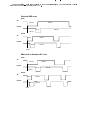
1
Rapports Techniques
N 153
UNITE DE RECHERCHE
INRIA-SOPHIA ANTIPOLIS
Programme 4
Robotique, Image et Vision
MD96 - A MULTI-DSP96002
BOARD
Institut National
de Recherche
en Informatique
et en Automatique
2004 route des Lucioles
B.P. 93
06902 Sophia-Antipolis
France
Herve MATHIEU
mai 1993
MD96 - A Multi-DSP96002 BOARD
Herve MATHIEU
INRIA-Projet Robotvis
bp 93
06902 Sophia Antipolis Cedex
Tel : 93 65 78 36 - Fax : 93 65 78 45
email [email protected]
May 10, 1993
Contents
1 MD96-TECHNICAL MANUAL
1.1 Introduction
1.2 MD96 Overview
1.3 DSP96002 Implementation
1.3.1 DSP96002 Overview
1.3.2 DSP96002 Mapping
1.4 Description of the MD96
1.4.1 Memory
1.4.2 Common Bus
1.4.3 DSP Host interface
1.4.4 Slave VMEbus Interface
1.4.5 Master VMEbus Interface
1.4.6 VMEbus Interrupt capability
1.4.7 DSP Interrupt facilities
1.4.8 Remote Reset
1.4.9 Use of the on-chip emulator : not yet implemented
1.5 Installation Guide of the MD96
1.5.1 Hardware necessities
1.5.2 On Board Jumper Installation
1.5.3 Note about Broadcast Capability
1.5.4 Software View
1.6 Some Figures about the MD96
1.6.1 Internal Access Time
1.6.2 VMEbus Access Time
1.6.3 Electrical and Mechanical Specication
1.6.4 Leds
1.6.5 MD96 Layout
1.7 System Integration and Communication
1.8 Future
3
: : : : : : : : : : : : : : : : : : : : : : : : : : : : : : : : : : : : : : : : : : : :
: : : : : : : : : : : : : : : : : : : : : : : : : : : : : : : : : : : : : : : : :
: : : : : : : : : : : : : : : : : : : : : : : : : : : : : : : : : : : :
: : : : : : : : : : : : : : : : : : : : : : : : : : : : : : : : : : :
: : : : : : : : : : : : : : : : : : : : : : : : : : : : : : : : : : :
: : : : : : : : : : : : : : : : : : : : : : : : : : : : : : : : : : : : :
: : : : : : : : : : : : : : : : : : : : : : : : : : : : : : : : : : : : : : : : : :
: : : : : : : : : : : : : : : : : : : : : : : : : : : : : : : : : : : : : : :
: : : : : : : : : : : : : : : : : : : : : : : : : : : : : : : : : : : :
: : : : : : : : : : : : : : : : : : : : : : : : : : : : : : : : :
: : : : : : : : : : : : : : : : : : : : : : : : : : : : : : : :
: : : : : : : : : : : : : : : : : : : : : : : : : : : : : :
: : : : : : : : : : : : : : : : : : : : : : : : : : : : : : : : :
: : : : : : : : : : : : : : : : : : : : : : : : : : : : : : : : : : : : : : :
: : : : : : : : : : : : : : : : : :
: : : : : : : : : : : : : : : : : : : : : : : : : : : : : : : : :
: : : : : : : : : : : : : : : : : : : : : : : : : : : : : : : : : : :
: : : : : : : : : : : : : : : : : : : : : : : : : : : : :
: : : : : : : : : : : : : : : : : : : : : : : : : : : :
: : : : : : : : : : : : : : : : : : : : : : : : : : : : : : : : : : : : : :
: : : : : : : : : : : : : : : : : : : : : : : : : : : : : : : : :
: : : : : : : : : : : : : : : : : : : : : : : : : : : : : : : : : : :
: : : : : : : : : : : : : : : : : : : : : : : : : : : : : : : : : :
: : : : : : : : : : : : : : : : : : : : : : : :
: : : : : : : : : : : : : : : : : : : : : : : : : : : : : : : : : : : : : : : : : : : :
: : : : : : : : : : : : : : : : : : : : : : : : : : : : : : : : : : : : : : :
: : : : : : : : : : : : : : : : : : : : : : : : : : : :
:::
: : : : : : : : : : : : : : : : : : : : : : : : : : : : : : : : : : : : : : : : : : : : :
2 MD96-SOFTWARE SUPPORT
2.1 Introduction
2.2 Software Installation
2.3 Building an application on the MD96
2.3.1 Host to MD96 code translation
2.3.2 MD96 mapping
2.3.3 How to Compile MD96 Code
2.3.4 Some C optimizations
2.4 MD96 On Board Library
2.4.1 VMEbus Access
2.4.2 Inter DSP Communication
2.4.3 Communication between MD96 and Host
2.4.4 Inter MD96 Communication
2.4.5 High Level Functions for MD96
2.5 MD96 Host Library
2.5.1 The Library
2.5.2 How to Compile on the Host machine with the MD96 library
19
: : : : : : : : : : : : : : : : : : : : : : : : : : : : : : : : : : : : : : : : : : : :
: : : : : : : : : : : : : : : : : : : : : : : : : : : : : : : : : : : : : : :
: : : : : : : : : : : : : : : : : : : : : : : : : : : : : :
: : : : : : : : : : : : : : : : : : : : : : : : : : : : :
: : : : : : : : : : : : : : : : : : : : : : : : : : : : : : : : : : : : : :
: : : : : : : : : : : : : : : : : : : : : : : : : : : : : :
: : : : : : : : : : : : : : : : : : : : : : : : : : : : : : : : : :
: : : : : : : : : : : : : : : : : : : : : : : : : : : : : : : : : : : : :
: : : : : : : : : : : : : : : : : : : : : : : : : : : : : : : : : : : : :
: : : : : : : : : : : : : : : : : : : : : : : : : : : : : : :
: : : : : : : : : : : : : : : : : : : : : : :
: : : : : : : : : : : : : : : : : : : : : : : : : : : : : : :
: : : : : : : : : : : : : : : : : : : : : : : : : : : : :
: : : : : : : : : : : : : : : : : : : : : : : : : : : : : : : : : : : : : : :
: : : : : : : : : : : : : : : : : : : : : : : : : : : : : : : : : : : : : : : :
1
3
3
6
6
6
7
7
7
8
8
8
9
9
9
9
9
9
10
12
12
13
13
13
15
15
16
17
17
: : : : : : : : : : : :
19
19
20
20
21
22
24
25
25
27
29
29
30
30
30
34
CONTENTS
2
2.6 Example of MD96 Applications
2.6.1 3x3 Convolution
2.6.2 Deriche Filter
2.6.3 Binocular Stereo Correlation
: : : : : : : : : : : : : : : : : : : : : : : : : : : : : : : : :
: : : : : : : : : : : : : : : : : : : : : : : : : : : : : : : : : : : : :
: : : : : : : : : : : : : : : : : : : : : : : : : : : : : : : : : : : : : : :
: : : : : : : : : : : : : : : : : : : : : : : : : : : : : :
3 MD96-HARDWARE SUPPORT
3.1 Introduction
3.2 Hardware Description
3.2.1 Data Transfers
3.2.2 VMEbus Slave Interface
3.2.3 VMEbus Interruption
3.2.4 DSP Module
3.2.5 Internal mapping
3.2.6 VMEbus Mastering
3.2.7 Timing Philosophy
3.2.8 OnCE
3.2.9 Bugs or things which can be better
3.2.10 Hardware Bugs
3.3 Software Description
3.3.1 Detail of the address decoder logic
3.3.2 DSP Mapping View
3.3.3 VMEbus Mapping View
3.4 Reserved memory space description
3.4.1 For the X Data memory eld
3.4.2 For the Y Data memory eld
3.4.3 For the Common memory
3.5 Schematics, Layout and PLDs
3.5.1 Hierarchical Design
3.5.2 VMEbus Interface
3.5.3 DSP Module
3.5.4 OnCE Interface
3.5.5 Layout
3.5.6 Programmed Logic Device
3.5.7 Integrated Circuit
34
34
35
35
37
: : : : : : : : : : : : : : : : : : : : : : : : : : : : : : : : : : : : : : : : : : : :
: : : : : : : : : : : : : : : : : : : : : : : : : : : : : : : : : : : : : :
: : : : : : : : : : : : : : : : : : : : : : : : : : : : : : : : : : : : : :
: : : : : : : : : : : : : : : : : : : : : : : : : : : : : : : : :
: : : : : : : : : : : : : : : : : : : : : : : : : : : : : : : : : :
: : : : : : : : : : : : : : : : : : : : : : : : : : : : : : : : : : : : : : :
: : : : : : : : : : : : : : : : : : : : : : : : : : : : : : : : : : : : :
: : : : : : : : : : : : : : : : : : : : : : : : : : : : : : : : : : :
: : : : : : : : : : : : : : : : : : : : : : : : : : : : : : : : : : : :
: : : : : : : : : : : : : : : : : : : : : : : : : : : : : : : : : : : : : : : : : : :
: : : : : : : : : : : : : : : : : : : : : : : : : : :
: : : : : : : : : : : : : : : : : : : : : : : : : : : : : : : : : : : : : :
: : : : : : : : : : : : : : : : : : : : : : : : : : : : : : : : : : : : : : :
: : : : : : : : : : : : : : : : : : : : : : : : : : :
: : : : : : : : : : : : : : : : : : : : : : : : : : : : : : : : : : :
: : : : : : : : : : : : : : : : : : : : : : : : : : : : : : : : :
: : : : : : : : : : : : : : : : : : : : : : : : : : : : : : :
: : : : : : : : : : : : : : : : : : : : : : : : : : : : : :
: : : : : : : : : : : : : : : : : : : : : : : : : : : : : :
: : : : : : : : : : : : : : : : : : : : : : : : : : : : : : : :
: : : : : : : : : : : : : : : : : : : : : : : : : : : : : : : : : :
: : : : : : : : : : : : : : : : : : : : : : : : : : : : : : : : : : : :
: : : : : : : : : : : : : : : : : : : : : : : : : : : : : : : : : : : :
: : : : : : : : : : : : : : : : : : : : : : : : : : : : : : : : : : : : : : :
: : : : : : : : : : : : : : : : : : : : : : : : : : : : : : : : : : : : : :
: : : : : : : : : : : : : : : : : : : : : : : : : : : : : : : : : : : : : : : : : : :
: : : : : : : : : : : : : : : : : : : : : : : : : : : : : : : :
: : : : : : : : : : : : : : : : : : : : : : : : : : : : : : : : : : : :
37
37
37
37
38
38
39
39
39
40
40
40
40
40
41
41
47
47
47
48
49
49
50
53
54
55
56
56
Chapter 1
MD96-TECHNICAL MANUAL
1.1 Introduction
MD96 is the name of the Multi-DSP 96002 board developed in Robotvis department (INRIA-Sophia),
during ESPRIT P940 European project, in 1989.
The MD96 is a high integrated board, using four Motorola 96002 Digital Signal Processors and
interfaced with the VMEbus.
This document is a general overview of the MD96, its synoptic, its performance and its installation
guide, with also an overview of the processor used.
Two other chapters are about the MD96. A Hardware Annexes explains in details how the MD96
works, it includes the schematics and the PLDs equations. A Software support gives the C functions
syntax of the MD96 library. These functions allows you to develop application on the MD96, it includes
functions to connect the MD96 and the Host machine (SUN, VxWorks system, ) and functions which
are internal functions of the MD96 (inter DSP communication, VMEbus accesses, DMA transfer, ).
This chapter consists of four parts :
:::
:::
The rst one provides a general view of the board. It explains the global architecture of the MD96,
then a general view of the processor, and some information about its implementation are given.
The second one gives a full description of the board, and explains the dierent element build around
the data path on the MD96.
The installation guide allows to insert the MD96 in a VMEbus system. Some gures about electrical
consumption, mechanical, and data transfer timing specications are also given.
The fourth part gives generalities about System Integration, Communication, and about future
expansion for the MD96.
The architecture of the MD96 allows a great reduction in terms of time computation in regard to a
workstation, if they t these requirements :
Firstly, application must use the maximum of the DSP 96002 features. That means, to have a great
amount of oating point operations, to use trigonometry (Look Up Table in the DSP 96002) or to
accept perfectly DSP 96002 memory mapping (X,Y,P elds).
Secondly, it must use the MD96 features. That means to be parallelized in a small number of tasks
(between 4 and 16), to use the inter-DSP communication, not to be too greedy in terms of memory
space (Only 9 Megabytes are available).
1.2 MD96 Overview
The MD96 is VMEbus interfaced board achieving a peak processing power of 240 MFLOPS.
The main features of the MD96 are :
3
CHAPTER 1. MD96-TECHNICAL MANUAL
4
Four Processing Elements (PE), working in parallel. Each PE is composed of a 96002 Digital Signal
Processor at 33 or 40 MHz and one or two JEDEC memory modules. The memory modules are
organized in 64Kx32, 128Kx32 or 256Kx32. Thus, each DSP can have 2 Mbytes of fast static
memory.
A On Board Shared bus between the four PE, the VMEbus and a Common memory (64 Kwords
to 256 Kwords). This Common memory is one JEDEC module of 64Kx32 up to 256Kx32. This
Common bus allows PE to create fast communication channels between them and to share data
using a Common memory. This memory could also be used by the VMEbus interface.
Each PE can be master or slave on the VMEbus allowing the board to work without any master
board. (except for boot operation). The VMEbus interface module is fully compliant with the VMEbus specication (Revision C.1). The interface is a module which is A32-D32 MASTER/SLAVE
(allowing 32-bit data transfers), A24-D32 MASTER/SLAVE and A24-D16 MASTER.
The Arbiter, Interrupter and Timer modules of the VMEbus specication are not provided on the
DSP board.
A Broadcast transfer can take place on the VMEbus to simultaneously access several MD96. It
allows a simultaneous write into the Common memory. Because Broadcast transfer is not support
by VMEbus, two external rows of the P2 connector are used to provide this feature.
Remote Reset facility for each PE is provided.
Interrupt generation facilities : The VMEbus interface is able to generate VMEbus interrupts with
programming interrupt levels and vectors. This function is used by the PE to provide synchronism
with the supervisor and is very ecient for real time application.
Each PE module can be interrupted by VMEbus. In fact you can activate three dierent interruptions by DSP.
A DSP OnCE (MOTOROLA Trademark) debug interface will be implemented on the MD96 to
debug the DSPs. This interface is mapped into the VMEbus world register mapping able to access
the serial OnCE DSP interface. This interface will be used later for high level debugging.
There is no need for a bootstrap memory EPROM on the board, since each DSP will be start up
from its Host interface. This feature saves four EPROM devices, but requires a Host intervention
at RESET. It allows a complete reconguration of the board, both for the user program and the
development tools.
The MD96 is constituted of standard CMOS/TTL components only, and is implemented on a
extended double Euro-Card (220 mm x 233 mm).
The MD96 accepts up to 9 Mega Bytes of fast access memory, which is useful to support C applications.
It eciently uses the dual port DSP capability. Each DSP can work in its Local memory (port B) with
zero Wait State and no bus arbitration, and the Common bus (port A) can be used by each DSP with
one Wait State, or by the VMEbus with a minimum of arbitration. (g 1 summarize the MD96 hardware
architecture).
1.2. MD96 OVERVIEW
5
MULTI DSP96002 BOARD
SRAM
512Kx32
SRAMSRAM
512Kx32
512Kx32
LOCAL BUS
LOCAL BUS
DSP
96002
DSP
96002
SRAM
512Kx32
LOCAL BUS
DSP
96002
SRAM
512Kx32
LOCAL BUS
DSP
96002
COMMON BUS
SRAM
256Kx32
VME
Interrupter
COMMON
MEMORY
On Board
Arbiter
VME INTERFACE
g 1 : summarize the board hardware architecture.
CHAPTER 1. MD96-TECHNICAL MANUAL
6
1.3 DSP96002 Implementation
1.3.1 DSP96002 Overview
The DSP96002 is the rst member of dual-port IEEE oating-point programming CMOS processor family.
The device is available either in 33 MHz or in 40 MHz clock, for 16,5 (or 20) Million Instructions per
second (MIPS). The processing core gives 49.5 (or 60) MFLOPS power per device.
The main features of the DSP96002 are :
A 32x32 bits oating-point and integer multiplier unit.
A 32/64 bits oating-point and integer ALU.
A full 32 bits Address Generation Unit.
2Kx32 bits internal memory (in three banks).
Two A32/D32 channels DMA controller.
Full compatibility with IEEE 32/64 oating point and integer data format. This means that format
conversions are not required. In fact, the internal device architecture has been made for ecient C
implementation.
Graphics applications have already been studied by MOTOROLA, including fast graphics instructions in the assembler language.
The DSP is dual ported, this means that input/output capabilities are double if compared to
standard DSP.
1.3.2 DSP96002 Mapping
The DSP96002 has 2 separate Data/program access buses (ports A and B) which allows for instance,
simultaneous access to an external data and to a program instruction. The separation of data and
program is really interesting in some cases, when program could not be located in the internal program
memory of the chip ( this memory is only 1K word). This functionality can increase the execution speed
in a 3/2 ratio.
The only limitation of this memory mapping is that the Common memory is a bottle neck for the
four DSP. Only applications with a low bandwidth on this bus can be implemented.
The internal program memory is left partially free for the user (512 words) allowing to use it as a
cache program memory for short critical routines. No bootstrapping EPROM is present on the board,
and an Host bootstrap loading is required at startup, it uses the rst 512 words..
The external Local memory will be used for both X,Y,P addressing spaces. The mapping of these
three memory banks has some over-lapping, thus to optimize the exibility of the memory. That means
that users have to build there software mapping during compilation. (Read MD96-Software Support for
more explanation).
The DSP 96002 is able to map up to 8 memory segments by space X, Y or P. For each segment we
choose the input/output port (A or B).
The following graph describes the segments implemented on the MD96 board :
Mem. segments
X0,Y0,P0
X1,Y1,P1
X2,Y2,P2
X3,Y3,P3
X4,Y4,P4
X5,Y5,P5
X6,Y6,P6
X7,Y7,P7
Addresses
Denition
$00000800,$1FFFFFFF Shared memory/OnCE/HOST/DMA
$20000000,$3FFFFFFF
Local memory access
$40000000,$5FFFFFFF extended o board VMEbus access 32
$60000000,$7FFFFFFF extended o board VMEbus access 32
$80000000,$9FFFFFFF
VMEbus access A16/D16 low
$A0000000,$BFFFFFFF
VMEbus access A16/D16 high
$C0000000,$DFFFFFFF
Reserved for future use
$E0000000,$FFFFFF7F
Reserved for future use
Port
Port A
Port B
Port A
Port A
Port A
Port A
Port A
Port A
The second parameter of the addressing ports are the Wait States. It depends on the memory access
time and the logic between the DSP and the memory. For the MD96, zero Wait State is achieve on
Local port and one Wait State is necessary due to logic for Common memory accesses.(The number of
1.4. DESCRIPTION OF THE MD96
7
Wait States is between 0x0 and 0xF). For VMEbus accesses this parameter is not used because VMEbus
is much slower than DSP, and a special hardware acknowledge is used. The number of Wait States is
between 0x0 and 0xF.
1.4 Description of the MD96
1.4.1 Memory
Memory conguration
Designers usually use static memory devices for real-time applications. These kinds of memories have
the major advantage of having a very fast access time, but the disadvantage of being expensive and only
available with small capacities.
On the other hand, dynamic memories have low prices (ratio is 1/10 with the same memory size), large
capacities, but are not fast enough for DSP applications. The new DSP generation has been designed to
accept both memories.
We have chosen large static memory JEDEC compatible memory modules in ZIP package oering a
reasonable cost and a very compact solution. It allowed to implement four PE.
The MD96 can receive 64K x 32 bits, 128K x 32 bits or 256K x 32 bits size with compatible pinout.
The static memory conguration is automatically detected by the MD96, but several memory maps can
be available using specic jumpers.
This exibility allows to have cheaper MD96 if a small memory area is sucient.
Most part of these Memory modules are on each Local bus, then the VMEbus can not access them
directly. The VMEbus can access them in indirect mode, the MD96's DMA capabilities make it available.
This transfer is also made in parallel with core execution. From the hardware point of view this solution
allows the removing of a 32 bits multiplexer interface per DSP and so saves place for other devices.
Memory and Wait state
During the Boot of the DSPs, the internal registers BCRA and BCRB have to be set. They indicate the
number of Wait states during external accesses.
The SRAM modules can be 64Kx32, 128Kx32 or 256Kx32, which are memories with zip64 standard
JEDEC format package.
The MD96 allows one Wait State on Common port and zero Wait State on Local port. The next
table gives more explanations.
For Common memory module :
DSP CLK Memory Access Time Wait State
33 MHz
40 MHz
25 ns
25 ns
1
1
For DSP's Local memory modules :
DSP CLK Memory Access Time Wait State
33 MHz
33 MHz
33 MHz
40 MHz
40 MHz
40 MHz
less than 25 ns
between 30 and 45 ns
between 50 and 75 ns
less than 20 ns
between 25 and 45 ns
between 50 and 75 ns
0
1
2
0
1
2
Note : The direct link between the DSP and its Local memory gives a very ecient channel of 80
Mbytes/sec.
1.4.2 Common Bus
Description
This Common Bus provides a link between the VMEbus, the DSPs and the Common memory.
The dierents ways to achieve data transfers can be enumerated as following :
CHAPTER 1. MD96-TECHNICAL MANUAL
8
The VMEbus can access the the shared memory in direct addressing.
The VMEbus can access the DSP Host interface which is also directly mapped. It provides a way
to access the Local memory of the DSPs, using the DMA mode.
Any DSP can access another one, by addressing its Host interface.
The VMEbus or any of the DSP can access the Status and Control registers of the MD96.
Common Bus Arbitration
The rules of arbitration of the MD96 Common bus are set to give the bus to the rst bus request, with a
priority to VMEbus transfers. This VMEbus priority is required to ensure fast VMEbus acknowledge on
any data transfer, avoiding spurious VMEbus timeout. But the Common bus is locked until the master
releases it.
In case of simultaneous requests, the priority given by the arbiter is rst the VMEbus, then DSP1,
then DSP2, then DSP3, and last DSP4.
A special board control bit allows a DSP to lock the Common bus. Read-Modify-Write access should
be used for this bit. This possibility must be used with many precaution to avoid VMEbus transfer
failures.
Another special control bit allows the VMEbus to lock the Common bus. Read-Modify-Write access
should also be used with this bit.
1.4.3 DSP Host interface
The DSP can congure its external ports either as a standard addressing port (master mode) or as a
Host interface (slave mode).
This exibility allows DSP to DSP direct communication through standard or DMA mode. In this
case, one DSP is in master mode and the other is in slave mode. For VMEbus accesses, the VMEbus
interface is in master mode and the DSP in the slave mode.
The DSP Host interface conguration allows a master to access the 16 internal registers of the DSP.
Some compatible VMEbus registers, such as interrupt vector register, has been implemented by Motorola
for VMEbus interface simplication.
1.4.4 Slave VMEbus Interface
the MD96 provides full MASTER/SLAVE VMEbus interface. The MD96 is mapped on the VMEbus as
two Mega Bytes memory.
The Slave interface consists of two topics :
An address decoder which decodes from A31 to A21. The MD96 accepts only A32/D32 and
A24/D32 transfers.
A DTACK generation which can be a standard DTACK or a Broadcast DTACK.
For all addresses and data, we use Latch transceivers instead of State drivers, this technique reduces
ground bounce and buses reectances, and it is quicker.
A Broadcast capability (writing the same data in several MD96 in one access) is implemented on the
MD96. A Broadcast address is fused in the PLD named DECODER and this address is Common for
the MD96 included in the Broadcast system. From the VMEbus point of view, this is a memory window
with the base address, the Broadcast address and with a size of one Meg Bytes which is the maximum
size of the Common memory.
Note that this Common address must be dierent than the Board base address. (Read Installation
Guide Section for more explanation)
1.4.5 Master VMEbus Interface
The following two parts requires notions about VMEbus.
The Master interface provides :
1.5. INSTALLATION GUIDE OF THE MD96
9
A bus requester to issue a VMEbus request. The MD96 board releases the bus at the end of its
transfers.
WARNING : You must be careful when using VMEbus access. The VMEbus signal Bus Clear
is not yet implemented, that means than a VMEbus timeout will occur if the DSP does too many
accesses. On solution is to use packets with a maximum of 256 data.
The bus request level used (BR0 - BR3) is software congurable in the Control register (BCR).
The Addresses Modier (AM0 - AM5) are software congurable in the Control register (BCR).
1.4.6 VMEbus Interrupt capability
Each DSP96002 can generate a VMEbus interruption. The level and the vector are software congurable
in the Control register (BCR). Each DSP has its own interrupt status bit. When cleared this bit indicates
that an interrupt is pending. A VMEbus interruption is active as soon as one of these bits is cleared.
The interrupter handler (Host machine) read these four bits to identify which DSP had asked for an
interruption. To disable the interruption the four bits must be set.
1.4.7 DSP Interrupt facilities
The VMEbus or one DSP can interrupt another DSP by three ways. In fact each DSP has three input
lines dedicated to these interruptions. They are activated by clearing a bit in the Control register (BCR).
(Read MD96-Hardware Support).
1.4.8 Remote Reset
Four bits in the Control register (BCR) are dedicated to control the hardware input reset of each DSP.
When cleared the DSP concerned is reset. Setting the bit allows the DSP to Boot.[7]
1.4.9 Use of the on-chip emulator : not yet implemented
The DSP96002's on-chip emulation (OnCE) circuitry provides a means of interacting with the DSP96002
and its peripherals non-intrusively so that the user may examine and change registers, memory or on-chip
peripherals. Breakpoints, trace, single and multiple steps functionalities are also provided.
The control of the four DSP units OnCE interface uses an 32 bits parallel shift register mapped in
the VMEbus interface.
1.5 Installation Guide of the MD96
1.5.1 Hardware necessities
VMEbus rack
The board is an extended VMEbus board (220x233 in millimeters) which is A32-D32 (or D16) Master or
Slave, that means that you need a VMEbus rack with a 233 millimeters width and a backplane using P1
and P2. [5]
DTACK daisy chain
This paragraph can be skipped if Broadcast access are not used.
When Broadcast transfer is used, a daisy-chain is provided to transmit the data transfer acknowledge
(DTACK) to the supervisor processor. Two pins of the external rows of the P2 connector are provided
for this DTACK generation (DTACKIN and DTACKOUT).
The gure following shows how to install the DTACKIN/DTACKOUT daisy chain :
CHAPTER 1. MD96-TECHNICAL MANUAL
10
DTACKIN/DTACKOUT daisy chain in P2 connectors
ROW
MD96
No3
MD96
No 2
MD96
No 1
MASTER
C B A
C B A
C B A
C B A
26
27
28
29
30
VME Backplane − Back View
1.5.2 On Board Jumper Installation
Most of the board's parameters are available by software. There is only two groups of jumpers to install,
the rst one concerns the the VMEbus transfers :
The base address of the MD96 has eleven address jumpers A31 to A21. They are compared to the
VMEbus address to validate a transfer. When ON, a jumper equals to 0.
Note that no jumper appears for Broadcast mode, thus because extended address (A31 to A24) are
the same for Broadcast or no Broadcast transfer and Broadcast addresses A23 to A21 are fused in
the PLD named DECODER (These addresses are 0,0,0).
There is one jumper for Address Modier Mode : when ON, only standard VMEbus transfers are
recognized, when OFF, only extended VMEbus transfers are recognized.
And one jumper when the VMEbus access the MD96 in Broadcast mode : when ON, the board
is considered as the last board for the DTACKIN-DTACKOUT daisy chain, when OFF, the board
actives the DTACKIN-DTACKOUT daisy chain as soon as it has nished the transfer.
If you don't use Broadcast transfers, this jumper can be set or reset.
The second group concerns the DSP memory mapping. There are several parameters concerning the
memory mapping :
Each Processor element can receive one or two modules of 64Kx32, 128Kx32 or 256Kx32.
The software has in charge to manage three memory elds : the program eld P, the data eld X
and The data eld Y.
A development system like the [4] for DSP96002 can force to separate X and Y elds when computing
oating point operations.
For each DSP96002, you have 4 hardware possibilities for the memory modules.
Two memory chips : one receives the X and P elds for the lower addresses and the Y eld for
the upper addresses. The other one receives the Y eld for lower addresses. The jumpers join,
DSP A17 to SRAM A17, DSP A16 to SRAM A16 and DSP A15 to SRAM A15 of the Static Ram.
1.5. INSTALLATION GUIDE OF THE MD96
11
One 256Kx32 memory chip : one jumper joins DSP A15 to SRAM A15 and DSP A16 to SRAM A16
of the Static Ram and the other one join an output of the DSPCTRL PLD to SRAM A17, to
separate the Y eld and the X/P eld. That means the software must take care when addressing
the P eld and the X eld.
Another solution is to join DSP A17 to SRAM A17, DSP A16 to SRAM A16 and DSP A15 to
SRAM A15 of the Static Ram, then you have mixed all the elds (X, Y, P).
One 128Kx32 memory chip : one jumper joins DSP A15 to SRAM A15 of the Static Ram and the
other one join an output of the DSP PLD to SRAM A16, thus to separate the Y eld and the X/P
eld. That means the software must take care when addressing the P eld and the X eld.
Another solution is to join DSP A16 to SRAM A16 and DSP A15 to SRAM A15 of the Static Ram,
then you have mixed all the elds (X, Y, P).
One 64Kx32 memory chip : a jumper joins an output of the DSP PLD to SRAM A15, thus to
separate the Y eld and the X/P eld. That means the software must take care when addressing
the P eld and the X eld.
Another solution is to join DSP A15 to SRAM A15 of the Static Ram, then you have mixed all the
elds (X, Y, P).
CHAPTER 1. MD96-TECHNICAL MANUAL
12
The next gure shows the location of jumpers for the dierent congurations.
1.5.3 Note about Broadcast Capability
The Broadcast addresses must be dierent from the base address of the boards. That means that the
jumpers A24 to A21 have to be dierent from the fused Broadcast addresses in the logical decoder chip
which are A23 = 0, A22 = 0, A21 = 0.
1.5.4 Software View
The MD96 is used as a powerful co-processor and is mapped as memory on VMEbus.
1.6. SOME FIGURES ABOUT THE MD96
13
Severals data paths between the VMEbus and the MD96 are provided.
The VMEbus can access :
the Common Memory by direct addressing.
one of the fourth DSP Local memory via the DSP Host interface..
the On Board registers to Boot and set your conguration.
A MD96 DSP can access :
another DSP to transfer data without interfering with the VMEbus..
the Common Memory. This memory is a communication memory but it can be also a data eld or
a program eld.
the On Board registers to set interrupt or to lock the VMEbus.
the VMEbus to access data or to control some process.
All the communication channels provide a very ecient way to program high level task, to use some
parallel tasks and to insert the MD96 in a complex system with other boards like acquisition boards or
axes-control boards.
1.6 Some Figures about the MD96
1.6.1 Internal Access Time
Access Type
DSP to Local memory
DSP to Common memory
DSP to DSP
Mbytes/sec
80
53.3
26.6
1.6.2 VMEbus Access Time
VMEbus Access
The access time is a constant. That means that the duration between AS and DTACK [5] is the same
when the VMEbus accesses, the Common Memory, the Control (BCR) and Status (BCSR) registers or
the DSP Host interface.
This duration equal 40 nanoseconds for a write access and 120 nanoseconds for a read access.
DSP VMEbus Access
VMEbus timing should be as short as possible to reduce access time to heavy data banks. These timing
have been optimized, but the transfer time depend of course, on the board accessed
Note : In the following table, STANDARD means for a C for with incremented counter, DO LOOP
means that the DSP 96002 was using its hardware DoLoop, and DMA means that we used the DMA
channel. [7]
WARNING : All the results showed below was obtain with two MD96 to MD96.
Mode
Read or Write Time (AS to AS) Megaword/sec Mbytes/sec
STANDARD
Read
600 ns
1.67
6.68
STANDARD
Write
380 ns
2.63
10.52
DO LOOP
Read
400 ns
2.5
10.0
DO LOOP
Write
250 ns
4.0
16.0
DMA
Read
400 ns
2.5
10.0
DMA
Write
250 ns
4.0
16.0
CHAPTER 1. MD96-TECHNICAL MANUAL
14
For more Details ... Here are the timing of the two major signals on VMEbus which are Address
Strobe (AS) and DaTa ACKnowledge (DTACK).
Standard VME acces
READ
AS
150 ns
450 ns
DTACK
70 ns
450 ns
120 ns
WRITE
AS
70 ns
310 ns
DTACK
60 ns
310 ns
40 ns
DMA mode or Hardware Do Loop
READ
AS
150 ns
240 ns
DTACK
70 ns
120 ns
WRITE
AS
60 ns
190 ns
DTACK
70 ns
40 ns
190 ns
240 ns
1.6. SOME FIGURES ABOUT THE MD96
15
1.6.3 Electrical and Mechanical Specication
This board has been designed in 1991 and routed on SUN workstations with Teradyne CAD.
It is made of 8 layers in Class 4, 6 for signals and two for power.
The board is constituted of standard CMOS/TTL compatible components only.
It is implemented on a extended double Euro-Card (220 mm x 233 mm) and is one slot width.
Maximum MD96 consumption is about 9.6 Amperes (with the maximum Memory Conguration).
CHIP
DSP96002
MEMORY MODULE
MEMORY MODULE
Standard logic
1.6.4 Leds
CONSUMPTION (mA) Number on the MD96
300
960 (working)
200 (idle)
70
4
5
4
40
There are seven leds on the MD96.
The upper one is the Reset Led. It indicates that at least one DSP is reseted.
The next one is the Slave Led, and is on when the VMEbus is accessing the MD96.
The third one is the Master Led, and indicates that the MD96 is accessing the VMEbus.
The last four DSP Leds, one for each DSP, indicate that a DSP is reseted or that it masters the
Common bus.
16
1.6.5 MD96 Layout
CHAPTER 1. MD96-TECHNICAL MANUAL
1.7. SYSTEM INTEGRATION AND COMMUNICATION
17
1.7 System Integration and Communication
The MULTI-DSP 96002 board can be used in any VMEbus compatible system. In general case, the
MD96 boards are managed by a supervisor CPU which uses them as fast slave task processors, and are
in charge of the following works :
Task scheduling and monitoring.
Data division and distribution.
Results collecting, and fusion.
Time synchronism.
DSP Host request interpretation.
Such tasks, are currently well managed by standard CPU processors.
A workstation with a VMEbus repeater or standard Real-Time operating systems like VRTX, OS9,
PSOS or VxWorks can be used. These standard operating systems provide the advantage to propose
additional facilities (display, mass storage, network communication).
1.8 Future
:::
In 1988, Gregory Randall (INRIA-Sophia) did the MD56, a Multi-DSP board with three Motorola DSP
56001. The experiment with the MD56 was very useful for the MD96 conception.
In 1990, another board with four DSP 96002 was born. The architecture was modify, but the experiment was also very useful.
Today, they are some other projects : A video interface for the MD96, it could be connected on the
Common bus and it could be design on a double Euro-Card. Another one is to do a new design with a
video interface for the MD96.
Wait and see !
18
CHAPTER 1. MD96-TECHNICAL MANUAL
Chapter 2
MD96-SOFTWARE SUPPORT
2.1 Introduction
MD96 is the name of the Multi-DSP 96002 board developed in Robotvis (INRIA-Sophia) department,
during ESPRIT P940 European project, in 1989.
The MD96 is a high integrated board, using four Motorola 96002 Digital Signal Processors and
interfaced with the VMEbus.
The architecture of the MD96 allows a great reduction in terms of time computation in regard to a
workstation, if they t these requirements :
Firstly, application must use the maximum of the DSP 96002 features. That means, to have a great
amount of oating point operations, to use trigonometry (Look Up Table in the DSP 96002) or to
accept perfectly DSP 96002 memory mapping (X,Y,P elds).
Secondly, it must use the MD96 features. That means to be parallelized in a small number of tasks
(between 4 and 16), to use the inter-DSP communication, not to be too greedy in terms of memory
space (Only 9 Megabytes are available).
This chapter consists of three parts :
The rst one gives information about Soft installation. It should be read after the Hardware
Installation found in previous chapter.
The second part explains how to build an application on the MD96.
The third one gives the libraries used for the MD96. It consists of one library for On Board program
and another one for driving the MD96 from a Host machine.
2.2 Software Installation
The libraries given in the following sections depend on the hardware conguration of the system. The
MD96 base addresses, the VMEbus interrupt level and vector and the VMEbus request level are dened
in a le
"hard.h"
read when libraries are compiled.
Here is a example of this included le.
/* ***** These defines depend NOT on hardware configuration */
/* This driver is able to drive up to 4 MD96 */
#define NB_BOARD_96_MAX 4
/* The MD96 was designed with 4 DSP */
#define NB_DSP_PER_BOARD 4
19
CHAPTER 2. MD96-SOFTWARE SUPPORT
20
/* When using a workstation with a VMEbus,
all the transfers go though /dev/vme32d32 */
#define BOARD_96DEVICE "/dev/vme32d32"
/* The MD96 is 2 mega-bytes width on VMEbus */
#define BOARD_96SIZE (2*1024*1024)
/* ---------------------------------------------------------------- */
/* ***** These defines depend on hardware configuration */
/* Just define the board physical address for the boards which are present */
#define BOARD0_96ADRESS 0x9F600000
#define BOARD0_ITLEVEL 3
/* VMEbus interrupt level [1 ... 7] */
#define BOARD0_ITVECTOR 0xE0 /* VMEbus interrupt vector [8 bits] */
#define BOARD0_VMELEVEL 3
/* VMEbus request level
[0 ... 3] */
/* This MD96 does not exist for the VMEVME configuration,
but exist for another configuration */
#ifndef VMEVME
#define BOARD1_96ADRESS 0x9f800000
#endif
#define BOARD1_ITLEVEL 3
#define BOARD1_ITVECTOR 0xE1
#define BOARD1_VMELEVEL 3
/* If this MD96 exist, insert the base address here
#define BOARD2_96ADRESS ??????????
*/
#define BOARD2_ITLEVEL 6
#define BOARD2_ITVECTOR 0x49
#define BOARD2_VMELEVEL 2
/* If this MD96 exist, insert the base address here
#define BOARD3_96ADRESS ??????????
*/
#define BOARD3_ITLEVEL 6
#define BOARD3_ITVECTOR 0x4a
#define BOARD3_VMELEVEL 2
/* This is the Broadcast address of the MD96s.
Only one Broadcast address is support.
All the MD96 included in the Broadcast system must have
the same beginning base address (0x9F) */
#define BROADCAST 0x9F000000
Refer to your System Manager for theses informations.
2.3 Building an application on the MD96
2.3.1 Host to MD96 code translation
The debugging on MD96 is not very easy, you must be condent with your code before proceeding to its
implementation.
Here are some requests to take codes running on your Host machine and to run them on the MD96.
The requirements for your software are :
2.3. BUILDING AN APPLICATION ON THE MD96
21
No printf and memory alloc. These functions exist but they can't work with the MD96 except if
you need very few memory space.
All big structure like tables must be dened as global at the beginning of the code. Then the Host
part of the code can read the table addresses and dump the data on the MD96.
A MD96 application is made of two kinds of codes. The rst one is the code running on your Host
machine. It uses the MD96 Host library and can provide the Boot initialization, the loading of code and
data and the dumping of results.
The second one is the code running on the MD96. It can be the same for each DSP or can be totally
dierent. This code consists of two things, one is user routines and the other one uses the MD96 On
Board library to provides communication and synchronism between DSPs, or VMEbus access, or VMEbus
interruption.
The following is about this second part of the code and gives you informations about the mapping of
you application and about the way to compile it.
2.3.2 MD96 mapping
As written in the C compiler manual, before compiling your code, you need to know where your will load
it. The DSP 96002 has no MMU, the user has in charge the mapping of his application, that means that
he has to choose where he will load his program and his data. It is a hard job, but it is very useful for
optimization. However, the locator le given as example is convenient for most of applications.
There is two kinds of memories. The Local memory and the Common memory. For most application
only the Local memory is used.
The Common memory is used when common data are shared by severals DSP on the same MD96.
The addresses are the same for X, Y and P elds and for the four DSPs.
Here is the description of the memory areas1 .
Program memory eld
$00000000 to $000001FF : Reserved. It contains the Boot code and is used to initialize some internal
registers and to run the C programs.
$00000200 to $000003FF : Internal Memory, is the best ecient eld to insert code. The Cross
Compiler uses this eld to insert the code created from some libraries. Critical functions can be forced
internally. For this, the locator le and the C le must be changed. See Pragma option in [4].
$20000000 to $2003FFFF : receives the extra code. $2003C000 to $2003FFFF is the standard area
and is enough for most applications.
All other segments are reserved.
X Data memory eld
This eld is only used for the stack coming from C code, for double data memory and for some parameters
coming from the Boot code.
$00000000 to $0000000F : reserved for Boot's parameters.
$00000010 to $000001FF : used to insert the C stack and all the doubles. This is a critical point
because of the width of this memory eld.
$00000200 to $000007FF : reserved for the trigonometric function given in the C libraries.
$00000800 to $000407FF : This is the Common memory area, including a Y and P space because
there is no separation on the Common Bus. (Read MD96-Technical Support)
$20000000 to $2003FFFF : used for special applications with a big amount of doubles or a very big
C stack. For most applications it is not used.
All other segments are reserved.
Y Data memory eld
$00000000 to $0000000F : reserved for Boot's parameters.
$00000010 to $000001FF : is used by the C stack, for doubles and for very critical global values to
optimize time computation.
1 All the Addresses are calculated for the standard memory conguration of the MD96 which is nine 256Kx32 modules.
Refer to your System Manager for theses informations.
CHAPTER 2. MD96-SOFTWARE SUPPORT
22
$00000200 to $000007FF : reserved for the trigonometric function given in the C libraries.
$00000800 to $000407FF : This is the Common memory, including a Y and P space because there is
no separation on the Common bus.
$20000000 to $2007FFFF : is used to insert all the data which can not be insert internally. $20000000
to $2007CFFF is the standard mapping.
All other segments are reserved.
Conclusion
Using the standard given locator le should avoid all these memory mapping problems, but if you need
to change it, you must take care of the memory overlapping problems. For instance, $20040000 to
$2007FFFF for Y eld is the same segment than $20000000 to $2003FFFF for X and P elds.
The following table gives the overlapping addresses.
Memory Module (Hardware) X and P Addresses
Common 256Kx32 Module
First 256Kx32 Module
Second 256Kx32 Module
00000800-0003FFFF
20000000-2003FFFF
-
Y Addresses
Port
00000800-0003FFFF Port A
20040000-2007FFFF Port B
20000000-2003FFFF Port B
2.3.3 How to Compile MD96 Code
To compile a program, you need two things : a locator le and source les.
You must have a locator le which indicates the mapping of your application.
An example of this Locator le :
-----
AUTHOR : Herve MATHIEU , INRIA-Sophia
DATE : fevrier 1993
TOPIC : Locator File
REFERENCE : Intermetrics (Intertools C compiler)
------------------------- MAPPING DE LA MD96 ---------------------------- PI
#0 to #400
-- PA
#400 to #40000 max
-- PB
#20000000 to #2007FFFF
-- XI & YI
#0 to #1FF
-- XA & YA
#200 to #401FF without ROM
-- XA & YA
#800 to #407FF with ROM
-- XB & YB
#20000000 to #2007FFFF
--------------------- CONVENTIONS COMMANDE RESERVE ---------------------I
, A ,
B
, R
-- Zone P
: pi
, pa , pb (=pe) , (pr)
-- Zone X
: xi (=xe) , xa , xb
, (xr)
-- Zone Y
: yi (=ye) , ya , yb
, (yr)
-- Zone X et Y: li = xi & yi
-laa = xa & ya (=la=le)
-lbb = xb & yb
-lab = xa & yb
-lba = xb & ya (=lb)
------------------------------------------------------------------------- Default (page 129 of intermetrics C cross-compilator 96002)
--- PI #000 - #3ff
-- XI #000 - #1ff
-- YI #000 - #1ff
-- PA #000 - #ffffffff
2.3. BUILDING AN APPLICATION ON THE MD96
-- XA #200 - #ffffffff
-- YA #200 - #ffffffff
-- PB #000 - #ffffffff
-- XB #200 - #ffffffff
-- YB #200 - #ffffffff
-- PR #000 - #3ff
ROM
-- XR #400 - #7ff ROM
-- YR #400 - #7ff ROM
------------------------- COMMANDES RESERVE ------------------------ Memory areas reserved for hardware and software reasons.
-- PROGRAM :
reserve ( pi : #000 to #200);
-- Boot Program
reserve ( pa : #000 to #800);
-- Internal Memory
reserve ( pa : after #40000);
-- Memory Max Size 256Kx32
reserve ( pb : before #2003C000);
-- Reserved for Data
reserve ( pb : after #20040000);
-- Memory Max Size 256Kx32
-- DATA
reserve
reserve
reserve
reserve
reserve
reserve
reserve
reserve
X
(
(
(
(
(
(
(
(
ET Y :
xi : #00 to #10);
-- For Boot Program
yi : #00 to #10);
-- For Boot Program
xa : #000 to #ffffffff);
-- No XA
ya : #000 to #800);
-- ROM (sin and cos)
ya : after #40800);
-- Memory Max Size 256Kx32
xb : #000 to #ffffffff); -- No XB
yb : before #20000000);
-- Beginning of YB
yb : after #2007C000);
-- Y Memory Max size 512Kx32
-- reserve ( xr : #0 to #ffffffff);
-- reserve ( yr : #0 to #ffffffff);
-- reserve ( pr : #0 to #ffffffff);
------------------------- COMMANDES MEMORY -----------------------memory ( pi : #400);
------------------------- COMMANDES START ------------------------- Program Start
locate ( init_PB
: b : #2003C000);
------------------------- COMMANDES LOCATE ------------------------- INTERNAL PROGRAM (PI) :
-- Si Interruption locate ( Sirqa_P : i : #00000200);
locate ( libcode_P
: i : after #00000200);
-- INTERNAL DATA (XI & YI et LI) :
-- Data initialisee long 64 bits
locate ( ildata_L
: i : after
#00000010);
-- Data non initialisee long 64 bits
locate ( uldata_L
: i : after
#00000010);
-- Data initialisee data 32 bits
locate ( idata_Y
: i : after #00000010);
-- Stack Area ... interne si petite (400 doubles) voir pmain.96k
locate ( S__STACK_LI : i : after #00000010);
-- DATA IN LOCAL MEMORY
-- Data non initialisee
locate ( udata_Y
:
locate ( sdata_Y
:
locate ( cdata_Y
:
(YB) :
data 32 bits
b : after #20000000);
b : after #20000000);
b : after #20000000);
23
CHAPTER 2. MD96-SOFTWARE SUPPORT
24
locate (class (usep)
locate (class (isep)
: b
: b
:
:
after #20000000);
after #20000000);
--- DATA IN COMMON MEMORY (YA) :
-- Use the C compiler pragma option for this area.
------------------------ FIN -------------------------
You must compile your MD96 code. This is an example of a Makele :
#
# AUTHOR : Herve MATHIEU
# DATE : 16 novembre 1992
# TOPIC : MAKEFILE for MD96 code
#
#
#
#
#
Notice :
ITOOLS & RTLIBS are Defines for Intertools C compiler package.
MD96LIB is define for the MD96 On Board Library.
See your System Manager for these PATHs.
CFILES = \
example1.c \
example2.c \
example3.c
HEXFILE=proto
CCFLAGS="-i"
LDFLAGS="-do"
LDLIBRARY=${RTLIBS}/libc96k.rom ${MD96LIB}/iolib/hmio.lib
# Others Libraries can be add for special systems
# ---------------------------------------------.SUFFIXES: .c .ol
.c.ol:
${ITOOLS}/c96002 $*.c ${CCFLAGS} -S ${RTLIBS}
# ---------------------------------------------all: ${HEXFILE}.hex
${HEXFILE}.hex : ${CFILES:.c=.ol}
${ITOOLS}/llink ${CFILES:.c=.ol}
${LDFLAGS} -L ${LDLIBRARY} -c ${HEXFILE}.cmd
${ITOOLS}/form96k ${HEXFILE}.ab
${ITOOLS}/gsmap ${HEXFILE}.ab -o
${ITOOLS}/symlist ${HEXFILE}.ab -o
${MYMD96}/mem ${HEXFILE}
# ---------------------------------------------clean:
/bin/rm -f ${CFILES:.c=.ol} ${HEXFILE}.ai ${HEXFILE}.ab ${HEXFILE}.s
# ----------------------------------------------
2.3.4 Some C optimizations
Some C instructions are better optimized when you take into account of some simple rules.
2.4. MD96 ON BOARD LIBRARY
25
For a FOR loop, the DSP96002 has a Hardware Do Loop which is twice better than a standard FOR
with a register incremented and compared to a xed value. The Compiler uses the best solution
only then the code in the FOR-loop is subroutineless.
For some very critical functions, you would better extract the parameters of all the function and
force the Compiler to place this code or these parameters internally. The DSP96002 has some
on-chip memory which is more ecient. [4]
The DSP96002 has a Floating point ALU, thus can do oating point operations at the rate of integer
operations.
2.4 MD96 On Board Library
All these functions allow a high level communication between the four DSP96002 in a MD96 board or
between a DSP96002 and the VMEbus.
2.4.1 VMEbus Access
Using Core Access
These functions are used by the DSP to access the VMEbus.
---------VMEbus Acces Control.
Release 1.0
--- Function with open/close
iovme_open : Open the VMEbus connection
iovme_write_short : Read a short
iovme_read_short : Write a short
iovme_transfer : Read or write data
iovme_close : Close the VMEbus connection
--- Function without open/close
iovme_write : Write data
iovme_read : Read data
----------> When 'VmeMode' is required in a function, it selects the address modifier
for VME bus acces.
Convention :
EXT_NON_PRI_DAT : extended non privileged data access
EXT_NON_PRI_PGM : extended non privileged program access
EXT_NON_PRI_BLK : extended non privileged block access
EXT_SUP_VIS_DAT : extended supervisory data access
EXT_SUP_VIS_PGM : extended supervisory program access
EXT_SUP_VIS_BLK : extended supervisory block access
STA_NON_PRI_DAT : standard non privileged data access
STA_NON_PRI_PGM : standard non privileged program access
STA_NON_PRI_BLK : standard non privileged block access
STA_SUP_VIS_DAT : standard supervisory data access
STA_SUP_VIS_PGM : standard supervisory program access
STA_SUP_VIS_BLK : standard supervisory block access
SHO_NON_PRI_ACC : short non privileged access
SHO_SUP_VIS_ACC : short supervisory access
default : extended non privileged data access
----------> When 'type' is required in a function, it selects the data format for
VME bus acces.
26
CHAPTER 2. MD96-SOFTWARE SUPPORT
Convention :
DATA_16_BIT 16 bits data
DATA_32_BIT 32 bits data
----void iovme_close()
>
This routine is used to close the VME bus connection.
If forgotten at the end of VME transfers, it lock the system.
----int iovme_open(VmeMode)
int VmeMode;
>
This routine is used to connect the MD96 to the VME bus.
Return OK or ERROR.
----int iovme_read(VmeMode,address_dsp,data_type,address_vme,size)
int VmeMode, address_dsp, data_type, address_vme, size;
>
It is used to transfer data on the VME bus without open_vme.
Read 'size' data with format 'data_type' from VME address 'address_vme'
to DSP address 'address_dsp'.
Return OK or ERROR.
----int iovme_read_short(address)
>
It is used to transfer data on the VME bus.
Must be used after open_vme in VmeMode SHO_NON_PRI_ACC or SHO_SUP_VIS_ACC.
Read data at VME address 'address'.
Return the value.
----void iovme_transfer(address_dsp,data_type,address_vme,size,rw)
int *address_dsp;
int data_type;
int *address_vme;
int size;
int rw;
>
It is used to transfer data on the VME bus. Must be used after open_vme.
If rw = READ, read 'size' data with format 'data_type' from VME address
'address_vme' to DSP address 'address_dsp'.
If rw = WRITE, write 'size' data from DSP address 'address_dsp' to
VME address 'address_dsp' with format 'data_type'.
----int iovme_write(VmeMode,address_dsp,data_type,address_vme,size)
int VmeMode, address_dsp, data_type, address_vme, size;
>
It is used to transfer data on the VME bus without open_vme.
Write 'size' data from DSP address 'address_dsp' to VME address
'address_dsp' with format 'data_type'.
Return OK or ERROR.
----void iovme_write_short(address,value)
2.4. MD96 ON BOARD LIBRARY
27
>
It is used to transfer data on the VME bus.
Must be used after open_vme in VmeMode SHO_NON_PRI_ACC or SHO_SUP_VIS_ACC.
Write 'value' at VME address 'address'.
Using DMA Access
These functions are used by the DSP to access the VMEbus. Using the DMA channel [7] provides high
performance data transfers and allows you to work on DSP96002 in parallel mode.
---------DMA Control.
Release 1.0
----int iodma(adr_sou, type_sou, adr_des, type_des, size)
int adr_sou, type_sou, adr_des, type_des, size;
>
This routine uses the DMA channel of the DSP. It loads 'size' data from
the 'adr_sou' address of 'type_sou' memory field to 'adr_des' address of
'type_des' memory field.
'type_sou' and 'type_des' are VMEBUS, MEM_P, MEM_X, MEM_Y.
Return Ok or ERROR.
2.4.2 Inter DSP Communication
These functions are used to communicate between DSP on the same MD96.
---------Inter-DSP Communication.
Release 1.0
--- Driving Functions
iodsp_run_dsp : run a DSP
--- Data Flow --iodsp_write_buffer : write data
iodsp_read_buffer : read data
--- Communication --iodsp_init_com : initialize inter-DSP communication
iodsp_write_com : write a flag in another DSP
iodsp_read_com : read a flag from another DSP
iodsp_identity : identification flag
----int iodsp_identity()
>
Return DSP1 for the first DSP.
Return DSP2 for the second DSP.
Return DSP3 for the third DSP.
Return DSP4 for the fourth DSP.
Use by the code to know on which dsp it runs.
----void iodsp_init_com()
28
CHAPTER 2. MD96-SOFTWARE SUPPORT
>
This routine is used for Communication between the DSPs on a MD96.
Initialize the Communication area.
----int iodsp_read_buffer(dsp_number, dsp_address, mem_type, buffer, size)
int dsp_number;
int dsp_address;
int mem_type;
int *buffer;
int size;
>
This routine is used to read data from one DSP to another DSP.
Read 'size' data from the dsp 'dsp_number', at the dsp address
'dsp_address' in the memory field 'mem_type', to the buffer beginning
at address 'buffer'. It use the DMA channel and should
be used for Local Memory.
Return Ok or ERROR.
----int iodsp_read_com(dsp_number)
int dsp_number;
>
This routine is used for Communication between the DSPs on a MD96.
Read the semaphore coming from the DSP 'dsp_number'.
'dsp_number' must be different from the DSP running the function.
Return value.
----int iodsp_run_dsp(dsp_number, start_address, with_it_vme)
int dsp_number;
int start_address;
int with_it_vme;
>
This routine is used to run a dsp.
Returns OK if the run has been done, ERROR if not.
with_it_vme = IT_ON [VME interrutpion at the end of the program]
with_it_vme = IT_OFF [no VME interrution]
Return Ok or ERROR.
----int iodsp_write_buffer(dsp_number, dsp_address, mem_type, buffer, size)
int dsp_number;
int dsp_address;
int mem_type;
int *buffer;
int size;
>
This routine is used to write data from one DSP to another DSP.
Write 'size' data in the dsp 'dsp_number' memory, at the dsp address
'dsp_address' in the memory field 'mem_type', from the buffer
beginning at the address 'buffer'. It use the DMA channel, must be
used for Local Memory and should not be used for Common memory.
Return Ok or ERROR.
----int iodsp_write_com(dsp_number,value)
int dsp_number;
int value;
2.4. MD96 ON BOARD LIBRARY
29
>
This routine is used for Communication between the DSPs on a MD96.
It writes the semaphore 'value' to the DSP 'dsp_number'.
'dsp_number' must be different from the DSP running the function.
Return Ok or ERROR.
2.4.3 Communication between MD96 and Host
These functions allow you to communicate with some semaphore 2 regardless of hardware.
---------Host Communication.
Release 1.0
----float md96_read_param_float(parameter_number)
int parameter_number;
>
This function is used for Communication between the MD96 and the Host.
Read the parameter 'parameter_number'. Should be write by the Host.
'parameter_number' should be PARAMETER_0, PARAMETER_1, ...
Return value.
----int md96_read_parameter(parameter_number)
int parameter_number;
>
This function is used for Communication between the MD96 and the Host.
Read the parameter 'parameter_number'. Should be write by the Host.
'parameter_number' should be PARAMETER_0, PARAMETER_1, ...
Return value.
----void md96_write_status(value)
int value;
>
This function is used for Communication between the MD96 and the Host.
Write value in the Status address. Should be read by the Host.
2.4.4 Inter MD96 Communication
All these functions are running on one MD96 board, and are used to access to DSP on other MD96
boards.
---------Inter-MD96 Communication.
Release 1.0
----int iomd96(dsp_number, its_address, my_address, size, rw)
int dsp_number;
int *its_address, *my_address;
2
Memory written by a DSP and read by another one to achieve synchronism between these DSPs
30
CHAPTER 2. MD96-SOFTWARE SUPPORT
int size;
int rw;
>
This function provides some communication between two MD96
on the same VMEbus.
If rw = READ, read 'size' data from the dsp 'dsp_number' at address
'its_address' to the address 'my_address'.
If rw = WRITE, write 'size' data from the address 'my_address' to the
dsp 'dsp_number' at address 'its_address'.
'dsp_number' should be DSP1, DSP2 ... and must be on another MD96.
Return Ok or ERROR.
2.4.5 High Level Functions for MD96
VMEbus interruption
---------VMEbus Interruption Control.
Release 1.0
----void ioit()
>
Use by one DSP to interrupt the VME bus.
2.5 MD96 Host Library
2.5.1 The Library
The name of all the functions running on the MD96 start with md96 .
----------> boot means to load the basic program in the dsp and to initialize it.
--- Driving Functions
md96_reset_all, reset all the DSPs.
md96_boot_all, initialize all the DSPs.
md96_run_dsp, run a dsp.
md96_run, run the four DSPs of one board.
md96_load_hex, load a .hex file in a dsp.
md96_load_pgm, load a program (.hex) file in a dsp.
--- Data Flow --md96_write_buffer, write a buffer via a DSP.
md96_read_buffer, read a buffer via a DSP.
md96_write_broadcast,write a buffer to severals MD96 Common memory.
md96_read_all_dsp, read a buffer from the four DSP of the same MD96.
md96_write_all_dsp, write a buffer in the four DSP of the same MD96.
--- Communication --md96_init_com, initialize the communication Host-MD96.
md96_write_parameter,write a parameter to the MD96.
md96_read_error, read the MD96 error status.
md96_read_status, read the MD96 status.
--- Interruption,
md96_get_it, read the VME interruption status of the MD96.
md96_irq, active a MD96 interruption.
2.5. MD96 HOST LIBRARY
----Common Notation :
-> board_number select a MD96.
You should use BOARD96_1, BOARD96_2 ..., define in includemd96.h
-> dsp_number select a DSP 96002
You should use DSP1, DSP2, DSP3 ..., define in includemd96.h
if dsp_number is between DSP1 and DSP4, the dsp is in the first MD96.
if dsp_number is between DSP5 and DSP8, the dsp is in the second MD96.
And so on ...
-> mem_type means X, Y or P field.
You should use MEM_P, MEM_X and MEM_Y, define in includemd96.h
----void md96_get_it(board_number,WhichDSP)
int board_number;
int *WhichDSP;
>
This routine is used to acknoledge a VME interruption.
WhichDSP must be a table of four integer. WhichDSP[i] equal IT_ON
if DSPi had activate its interruption else IT_OFF.
----void md96_init_all()
>
This routine is used to initialize all the dsps in all the MD96.
(Boot, VME interruption, ...)
----void md96_init_com(board_number)
int board_number;
>
This routine is used for Communication between the Host and the MD96.
Initialize the Communication area.
----void md96_irq(dsp_number,WhichIrq)
int dsp_number;
int WhichIrq;
>
This routine is used to interrupt the dsp 'dsp_number' with one of its
three interrupt inputs which are IRQA, IRQB, IRQC (WhichIrq).
----int md96_load_hex(dsp_number, file_name)
int dsp_number;
char file_name[];
>
This routine is used to load a file to a dsp.
The file must be in hex format.
Return OK or ERROR.
----int md96_load_pgm(dsp_number, file_name, start_address)
int dsp_number;
char file_name[];
int *start_address;
>
This routine is used to load a program file to a dsp.
The program must be in hex format.
31
32
CHAPTER 2. MD96-SOFTWARE SUPPORT
'start_address' is the start address of the program and is read at
the end of the program file. It can be used with the function run_dsp.
Return OK or ERROR.
----void md96_read_all_dsp(board_number,address,buffer,size)
int board_number;
int address;
int *buffer;
int size;
>
Used to read 'size' data from the four DSPs (Local Memory) of the
board 'board_number' at 'address' to the 'buffer'.
The first quater from DSP1, the second from DSP2 and so on.
board_number should be BOARD96_1, BOARD96_2 ,...
----int md96_read_buffer(dsp_number,dsp_address, mem_type, buffer, size)
int dsp_number;
int dsp_address;
int mem_type;
int *buffer;
int size;
>
This routine is used to read data from the MD96 to the Host.
Read 'size' data from the dsp 'dsp_number', at the dsp address
'dsp_address' in the memory field 'mem_type', to the buffer beginning
at address 'buffer'. It uses the DMA channel and should
be used for Local Memory.
Return OK or ERROR.
----void md96_read_com(board_number,com_address, buffer, size)
int board_number;
int com_address;
int buffer[];
int size;
>
This routine is used to read 'size' data from the address 'com_address'
in the Common memory to the buffer beginning at address 'buffer' of
the board 'board_number'. It must be used only for Common memory.
----int md96_read_error(dsp_number)
int dsp_number;
>
This routine is used for Communication between the Host and the MD96.
Allow to read an error register in the Common memory.
Return Error value.
----int md96_read_status(dsp_number)
int dsp_number;
>
This routine is used for Communication between the Host and the MD96.
Allow to read a status register in the Common memory.
Return Status value.
-----
2.5. MD96 HOST LIBRARY
void md96_reset_all()
>
This routine is used to reset all the dsps for all the MD96.
----void md96_run(board_number)
int board_number;
>
This routine is used to run all the dsp on a board via MD96 interrupts.
----int md96_run_dsp(dsp_number, start_address, with_it_vme)
int dsp_number;
int start_address;
int with_it_vme;
>
This routine is used to run a dsp.
The `start_address` depends upon the program map.
Returns OK if the run has been done, ERROR if the start_address is
undefined. If go_address is zero, the program is run at the start
address defined by the compiler.
with_it_vme = IT_ON [VME interrutpion at the end of the program]
with_it_vme = IT_OFF [no VME interrution]
Return OK or ERROR.
----void md96_status(board_number)
int board_number
>
This function is used to know the MD96's memory configuration.
This routine prints the results (fprintf(stderr)).
----void md96_write_all_dsp(board_number,address,buffer,size)
int board_number;
int address;
int *buffer;
int size;
>
Used to load 'size' data from the 'buffer' to the four DSPs (Local Memory)
of the board 'board_number' at 'address'. The first quater for DSP1
and so on.
board_number should be BOARD96_1, BOARD96_2 ,...
----void md96_write_broadcast(com_address, buffer, size)
int com_address;
int buffer[];
int size;
>
This routine is used to write 'size' data from the buffer 'buffer' to
the Common memory at address 'com_address', with broacast accesses.
It must be used only for Common memory.
----int md96_write_buffer(dsp_number,dsp_address, mem_type, buffer, size)
int dsp_number;
int dsp_address;
int mem_type;
33
CHAPTER 2. MD96-SOFTWARE SUPPORT
34
int *buffer;
int size;
>
This routine is used to write data from the Host to the MD96.
Write 'size' data in the dsp 'dsp_number' memory, at the dsp address
'dsp_address' in the memory field 'mem_type', from the buffer
beginning at the address 'buffer'. It uses the DMA channel, must be
used for Local Memory and should not be used for Common memory.
Return OK or ERROR.
----void md96_write_com(board_number,com_address, buffer, size)
int board_number;
int com_address;
int *buffer;
int size;
>
This routine is used to write 'size' data from the buffer beginning
at address 'buffer' to the Common memory at address 'com_address'
of the board 'board_number'. It must be used only for Common memory.
----void md96_write_param_float(dsp_number,parameter_number,value)
int dsp_number;
int parameter_number;
float value;
>
This routine is used for Communication between the Host and the MD96.
Allow to give parameters to the application program via the
Communication memory.
----void md96_write_parameter(dsp_number,parameter_number,value)
int dsp_number;
int parameter_number;
int value;
>
This routine is used for Communication between the Host and the MD96.
Allow to give parameters to the application program via the
Communication memory.
2.5.2 How to Compile on the Host machine with the MD96 library
Your have to insert two things in your Makele, the include path for includemd96.h and the library path
for the MD96 Host library.
MD96INCLUDE = /u/..
MD96LIBPATH = /u/..
MD96LIB = libmd96.a or md96Lib.o or ..
For theses informations refer to your System Manager.
2.6 Example of MD96 Applications
2.6.1 3x3 Convolution
The 3x3 convolution has been implemented in 96K assembler.
2.6. EXAMPLE OF MD96 APPLICATIONS
AUTHOR
DATE
SOFT
SYSTEM
:
:
:
:
35
Herve MATHIEU
February 1993
3x3 Convolution (96K Assembler)
MVME167 + VxWorks
INPUT : Image of Intensity - 512x256 - Float
OUTPUT : Image after Convolution - 512x256 - Float
MD96
: one DSP used (40 Mhz)
main program in Internal memory
input in Local memory
outputs in Common memory
EXECUTION TIME : 2 (1/10 second)
2.6.2 Deriche Filter
This lter has been implemented in C and compiled without optimization.
AUTHOR
DATE
SOFT
SYSTEM
:
:
:
:
Herve MATHIEU
February 1993
Deriche Filter
MVME167 + VxWorks
INPUT : Image of Intensity - 256x256 - Float
OUTPUT : Image Gradient X and Y - 256x256 - Float
MD96
: one DSP used (40 Mhz)
main program in Local memory
input in Local memory
outputs in Common memory
REFERENCE : time on SS10 is 22 (1/10 sec)
EXECUTION TIME : 17 (1/10 second)
2.6.3 Binocular Stereo Correlation
This program includes a image Rectication, a oating-point Correlation and a 3D Reconstruction. The
implementation has been described in [2].
This table shows the time execution for the three algorithms implemented. The image is 256 256,
the disparity width is 20 and the correlation window is 7 7.
Algorithm
Rectication 2 images
Correlation sub-pixel
Reconstruction 3D
Total
DSP used MD96 SPARC 2 DSP/SUN
2
4
4
2-4
2.1 sec.
7.9 sec.
1.1 sec.
11.1 sec.
4.5 sec.
36.8 sec.
4.9 sec.
46.2 sec.
2.14
4.66
4.45
4.16
36
CHAPTER 2. MD96-SOFTWARE SUPPORT
Chapter 3
MD96-HARDWARE SUPPORT
3.1 Introduction
Reading this part requires knowledge about the VMEbus, the Motorola DSP 96002, and Programmed
Logic Devices (PLD). It is quite technique part, whereas only for people working with the MD96, without
any hardware development can skip this chapter.
3.2 Hardware Description
To understand how the MD96 is working, you have to take this technical manual, A3 schematics, the
PLD's equations and the referenced books.
3.2.1 Data Transfers
Severals data paths between the VMEbus and the MD96 are provided.
The VMEbus can access :
the Common Memory by direct addressing.
one of the fourth DSP Local memory via the DSP Host interface..
the On Board registers to Boot and set your conguration.
A MD96 DSP can access :
another DSP to transfer data without interfering with the VMEbus..
the Common Memory. This memory is a communication memory but it can be also a data eld or
a program eld.
the On Board registers to set interrupt or to lock the VMEbus.
the VMEbus to access data or to control some process.
The 74FTC646 buers are controlled by the PLD BUFCLK for the latchs (CPAB and so on) and by
PLD BUFDIR for the drives (EN and SR).
3.2.2 VMEbus Slave Interface
Address Decoder
Lines A31 to A24 are compared with STRA31 to STRA24 in the 74FCT512. The result is DEC.
In the PLD DECODER ...
The last three Address A23 to A21 are compared rst to STRA23 to STRA21 and after to (0,0,0)
which is the low Broadcast address for each MD96 board.
The jumper MOD24 allows, when accepting the Address Modier, to choose between standard and
extended transfers.
LW and A1 are here to be sure that only D32 transfers are taken place.
37
CHAPTER 3. MD96-HARDWARE SUPPORT
38
INT ASK provides a acknowledge to give the interrupt vector.
When all those conditions are on, the PLD DECODER generates the signals BRV to the PLD ARBITER or (inclusive) the signal Broadcast for the DTACK generation. The signal DTACK D is a security
to not release BRV before the end of the transfer.
Arbitration
At each clock rise, the PLD ARBITER gives the common bus to one of the VMEbus, the DSP1, the
DSP2, the DSP3 and the DSP4. As input we have the ve BR (Bus Request) which are BRV for the
VMEbus and BR1, BR2, BR3, BR4 for the four DSPs.
To have no access conict, the PLD ARBITER controls the line BB (Bus Busy) which is describe in
the DSP96002 User's Manuel.
The VMEbus can lock the Common Bus with LOCK ARB. Any DSP can do the same with
BCSR BRV.
DTACK Generation
The DTACK line is active when :
The VMEbus writes on the board, the DTACK can be validated as soon as the address and the
data are latched, that means when A CAB is asserted. (D CAB is asserted at the same time)
The VMEbus is reading, we have to wait LAR30CLK to be asserted. LAR30CLK shows that the
internal transfer is nished and that the data are latched in the 74FCT646 buers, which drive
those signals on the VMEbus. (LAR30CLK is the signal who latchs the data too)
When a Broadcast transfer takes place, the DTACK is asserted only if the board is the last board
concerned by the Broadcast transfer. If the jumper STR LAST is ON, the board is the last one, if
not DTACKIN-DTACKOUT daisy-chain is activates on the rst MD96, then on the second MD96 if its
transfer is nished until the last MD96 (jumper STR LAST is OFF) which activate the DATCK line.
The DTACK signal is released when all the transfer are nished, that means when DS (VMEbus data
strobe) and LAR30CLK are released.
3.2.3 VMEbus Interruption
A OR between the four IT DSP of the BCR register (PLD ITREGISTER) generates an IT signal. This
signal is mixed which the three bits BCR INT1, BCR INT2 and BCR INT3 of the BCR, which indicate
the VMEbus interrupt level,
When the IACKIN-IACKOUT daisy-chain goes in the MD96, it does not propagate it but generates
an INT ASK, to obtain the Common bus and to deliver the interrupt vector which is in a 74ALS996
(part of the BCR register).
IT is released when all the IT DSP are released (like any OR !).
INT ASK is released at the end of the acknowledge transfer, that means when AS and IACK IN are
released.
If the IACKIN-IACKOUT daisy-chain go in the MD96 and the MD96 has no interrupt pending, the
signal go though the MD96.
3.2.4 DSP Module
Port B
The only possible transfers on this port are from the DSP to the memory, so there are no conicts and
arbitration is not necessary. (BG grounded)
The local memory can be accessed by this port. The 32 data and the 15 lowest addresses lines are
directly connected.
The addresses A15, A16, A17 go though one ve-jumpers and though the PLD 20L8 DSP CONTROL.
S0, S1 select P, X or Y memory elds. BCSR PD1, BCSR PD0, and BCSR PD11 inform the PLD
DSP CONTROL about the memory modules. Each DSP can receive two memory modules of size 64K,
128K or 256K.
All these signals are put together to select the good memory module by(CS and ONE). ONE is used
to separate Y data eld and X+P eld when we have only one memory module.
3.2. HARDWARE DESCRIPTION
39
An equation in the PLD DSP CONTROL control the mapping of the memory. It can be change for
special applications.
The input R W is the reverse of the output OE. TS and BS are used for timing considerations : Only
TS is used if we have a 20L8-5ns PLD with 0 Wait State, and TS+BS is used if we have a 10ns PLD
with one Wait State.
Port A
The arbitration is made by the PLD ARBITER described before.
The data and address busses are connected to the common busses.
In the PLD MEMORY, the highest addresses, A31, A30, A29 and A28 are used to select the communication memory (CS), the VMEbus (OR V BR, LW, A1), the Host interface of another DSP (OTHER)
or the MD96 registers (OTHER).
3.2.5 Internal mapping
The three PLDs MEMORY, DMA and REGISTER provide a multiplexer system with two inputs (VMEbus addresses or DSPs addresses) and three outputs (Communication Memory, the Host interface of a
DSP or one of the On Board registers (BSR or BCSR).
On the VMEbus side we decode A18 (which is A20 on the VMEbus) to separate the Communication
Memory (CS) and the other part. For this part we decode A15, A14, A13, A12 to switch between a host
interface (HS1, HS2, HS3, HS4, HA1, HA2, HA3, HA4) or a register (BCR, BCSR, ONCE).
On the DSP 96602 side we decode A31, A30, A28 to separate the Communication Memory, the
VMEbus (as master) and the rest, and into the rest we decode A15, A14, A13, A12 to switch between a
host interface (HS1, HS2, HS3, HS4, HA1, HA2, HA3, HA4) or a register (BCR, BCSR, ONCE).
NOTICE : The OnCE interface is not yet implemented.
3.2.6 VMEbus Mastering
When one DSP96002 wants to master the VMEbus, it has to assert the BCR V BR (in the BCR register).
This line will do the VMEbus request. The BCR V BR line is mixed with the two bits BCR BR0 and
BCR BR1 (VMEbus request level) in the BCR register to request the VMEbus. When the BGIN-BGOUT
daisy chain is driven, the board keeps the line and take the VMEbus. The bit VBA which is the same as
the VMEbus line BBSY shows that the MD96 owns the VMEbus. The DSP96002 has only to pool this
bit in the BCSR register and if it is asserted, to access the VMEbus.
To perform a standard VMEbus access, AS, DS0 and DS1 are driven 40 ns after the busses. That the
second job of the PLD VMETIMING and the Delay Line chip.
When writing, the data and address busses are latched into the buers, then TA is asserted. To avoid
two consecutive DSP accesses, TA remains high (active low) until the end of the transfer.
When reading, the addresses are latched and TA is asserted when the VMEbus DTACK is asserted.
3.2.7 Timing Philosophy
VMEbus View
The transfer is between the VMEbus and an object which can be the Communication Memory or a
register or the Host interface of one DSP.
The philosophy is :
The addresses or the data need about 10 ns to go though the input buers where they are latched.
Then it takes 30 ns (after having set all the control lines) to write the data into the object or to
be able to read a data from the object. 30 ns is the slowest time and represents a security time to
access to 25ns memories. That means that for slower communication memory (for instance 70ns),
we have to change the 100ns delay line chip by a slower one (for instance 300ns).
When reading, data need 10 ns to go from the object to the output buers.
The PLD VMETIMING and the Delay Line chip are in charge of those timings.
CHAPTER 3. MD96-HARDWARE SUPPORT
40
DSP96002 View
The two major ideas are :
The data are warranted at least 6 ns after TS is deasserted when the DSP 96002 is writing.
There is no hold time after TS deasserted when the DSP 96002 is reading.
When reading there is no problem, we can have always 0 wait state.
when writing ...
The two PLDs interested by this are on the B port DSP CONTROL, and on the A port MEMORY
and REGISTER.
If these PLDs are 20L8-5ns we can have 0 Wait State with the TS pulse when writing.
If these PLDs are 20V8-10ns we have to insert one wait state and to generate a pulse with TS and
BS.
The TA of the DSP is asserted as soon as we know where the DSP want to go, except for VMEbus
read access where TA wait for the VMEbus DTACK.
3.2.8 OnCE
Not yet implemented.
3.2.9 Bugs or things which can be better
VME A1, VME A2 and VME A3 are used for data transfers and interrupt acknowledges. These
VMEbus lines should have only one load per board ... Each of these lines have two loads on the
MD96.
For the VMEbus specication (rev C1), during a read transfer you must wait 25 ns after having
received DTACK, to latch the data. The condition is not true.
When the DSP 96002 reads the BCR register to modify it (read-modify-write access), this DSP
should lock the common bus to be sure that no one else could change the register between the read
and the write accesses. The line BUSLOCK should be used for this but it is not. The DSP can use
the bit ARB LOCK in the BCR to lock the Common bus.
3.2.10 Hardware Bugs
Because the DSP TA (Transfer acknowledge) was not synchronous latch with the DSP clock, it did not
work.
Two straps and two pins out of their support make it possible :
The rst one in between the pin 14 of the PLD ARBITER and the pin 1 of the PLD BUFCLK
which must be out of his support.
The second one in between the support pin 1 of the PLD BUFCLK and the pin 6 of the PLD
BUFCLK which must be out of his support.
3.3 Software Description
3.3.1 Detail of the address decoder logic
From the VMEbus view, the board is decoded using A21 to A31, for single board access. For Broadcast
accesses, the addresses lines A24 to A21 are compared to the three Broadcast bits (0,0,0).
Note that the addresses lines are shifted from VMEbus backplane and the DSP addresses,
to manage the 32 bits data transfers correctly. VME A31 to VME A02 correspond to
DSP A29 to DSP A0, thus 32 bits data transfers are considered by the VMEbus world as
4 bytes increment.
3.3. SOFTWARE DESCRIPTION
41
3.3.2 DSP Mapping View
The memory mapping viewed by the DSP is for high addresses :
Address
$00000000-$0FFFFFFF
$10000000-$1FFFFFFF
$20000000-$3FFFFFFF
$40000000-$7FFFFFFF
$80000000-$9FFFFFFF
$A0000000-$BFFFFFFF
$C0000000-$FFFFFFFF
A31 A30 A29 A28 DSP addresses lines
0
0
0
0
1
1
1
0
0
0
1
0
0
1
0
0
1
x
0
1
x
0
1
x
x
x
x
x
Shared memory
OnCE HOST DMA
Local memory access
VMEbus A32 D32
VMEbus A24 D16 low bits
VMEbus A24 D16 high bits
future use
Port
A port
A port
B port
A port
A port
A port
A port
For the part Registers OnCE HOST DMA the memory mapping is :
Oset Address A15 A14 A13 A12 Comment
$10000000
$10001000
$10002000
$10003000
$10004000
$10005000
$10006000
$10007000
$10008000
$10009000
$1000A000
$1000B000
$1000C000
$1000D000
$1000E000
$1000F000
0
0
0
0
0
0
0
0
1
1
1
1
1
1
1
1
0
0
0
0
1
1
1
1
0
0
0
0
1
1
1
1
0
0
1
1
0
0
1
1
0
0
1
1
0
0
1
1
0
1
0
1
0
1
0
1
0
1
0
1
0
1
0
1
DSP1 DMA mode
DSP2 DMA mode
DSP3 DMA mode
DSP4 DMA mode
BCR Register access
BCSR Register access
Debugger Register access
Debugger access
DSP1 HOST (Interrupt) mode
DSP2 HOST (Interrupt) mode
DSP3 HOST (Interrupt) mode
DSP4 HOST (Interrupt) mode
DSP1 HOST (Pooling) mode
DSP2 HOST (Pooling) mode
DSP3 HOST (Pooling) mode
DSP4 HOST (Pooling) mode
When you access the HOST of one DSP, you access one of the sixteen registers inside the DSP. Here
is the mapping of these registers.
Oset Address A5 A4 A3 A2 Comment
$00000000
$00000004
$00000008
$0000000C
$00000010
$00000014
$00000018
$0000001C
$00000020
$00000024
$00000028
$0000002C
$00000030
$00000034
$00000038
$0000003C
3.3.3 VMEbus Mapping View
0
0
0
0
0
0
0
0
1
1
1
1
1
1
1
1
0
0
0
0
1
1
1
1
0
0
0
0
1
1
1
1
0
0
1
1
0
0
1
1
0
0
1
1
0
0
1
1
0
1
0
1
0
1
0
1
0
1
0
1
0
1
0
1
TX Y w
TX Y r
TX X w
TX X r
TX P w
TX P r
reserved
reserved
ICS
SEM
RXTXreg
reserved
IVR
CVR
reserved
reserved
To obtain the correct address decoder, you have to add the base address of the board which is dened
with jumpers.
The memory mapping of the part Shared memory OnCE HOST DMA is :
CHAPTER 3. MD96-HARDWARE SUPPORT
42
Oset Address V A17 V A16 V A15 V A14 Comment
$000000
$100000
$104000
$108000
$10C000
$110000
$114000
$118000
$11C000
$120000
$124000
$128000
$12C000
$130000
$134000
$138000
$13C000
x
0
0
0
0
0
0
0
0
1
1
1
1
1
1
1
1
x
0
0
0
0
1
1
1
1
0
0
0
0
1
1
1
1
x
0
0
1
1
0
0
1
1
0
0
1
1
0
0
1
1
x
0
1
0
1
0
1
0
1
0
1
0
1
0
1
0
1
Shared memory access
DSP1 DMA mode
DSP2 DMA mode
DSP3 DMA mode
DSP4 DMA mode
BCR Register access
BCSR Register access
Debugger Register access
Debugger access
DSP1 HOST (Interrupt) mode
DSP2 HOST (Interrupt) mode
DSP3 HOST (Interrupt) mode
DSP4 HOST (Interrupt) mode
DSP1 HOST (Pooling) mode
DSP2 HOST (Pooling) mode
DSP3 HOST (Pooling) mode
DSP4 HOST (Pooling) mode
When you access the HOST of one DSP, you access one of the sixteen registers inside the DSP. Here
is the mapping of these registers.
Oset Address V A7 V A6 V A5 V A4 Comment
$00000000
$00000010
$00000020
$00000030
$00000040
$00000050
$00000060
$00000070
$00000080
$00000090
$000000A0
$000000B0
$000000C0
$000000D0
$000000E0
$000000F0
0
0
0
0
0
0
0
0
1
1
1
1
1
1
1
1
0
0
0
0
1
1
1
1
0
0
0
0
1
1
1
1
0
0
1
1
0
0
1
1
0
0
1
1
0
0
1
1
0
1
0
1
0
1
0
1
0
1
0
1
0
1
0
1
TX Y w
TX Y r
TX X w
TX X r
TX P w
TX P r
reserved
reserved
ICS
SEM
RXTXreg
reserved
IVR
CVR
reserved
reserved
How to address the MD96 board
You have to sum the dierent osets concerning the register or the memory you want access.
As Example :
To access the BCR from the VMEbus ... BASE ADDRESS + 110000
To access the ICS register of DSP 3 from the VMEbus ... BASE ADDRESS + 138000 + 80
To access the beginning of the Communication memory from the VMEbus ... BASE ADDRESS + 0
To access the BCSR from one DSP ... 10005000
To access the SEM register of DSP 1 from one other DSP ... 1000C000 + 24
To access the beginning of the Communication Memory from one DSP ... 800
BE CAREFUL : you can not access (except during Boot) the beginning of the Communication memory
because the address 0 concerns the internal memory of the DSP !
Note about Broadcast Capability
It is sometimes necessary to load the same data to severals MD96. The VMEbus interface supports the
Broadcast of data (write cycles only) for some or for all the boards in VMEbus. One Broadcast address
is associated to this type of transfer.
3.3. SOFTWARE DESCRIPTION
43
The board address has 11 bits. For a group of boards which are interested by Broadcast transfers,
there are some conditions :
The boards must have the same Broadcast address, so they must have the same address bits A31 to
A24. That means that only 7 boards can be interested by the same Broadcast transfer. For the last
address bit A23 to A21, there is one address for the Broadcast address and seven for the dierent board
addresses.
Note that you can have more than one Broadcast group.
Detail of the DSP control and status registers
All the board registers are mapped in the VMEbus addressing space and in the DSP addressing space,
so that any external board or any internal PE could use the resources shared on the common board bus
and the VMEbus.
There are two major registers on the MD96 :
1. the BCR ( Board Control register)
The BCR register should be accessed in read/modify/write access. It means that this register must
be read before it is modied. The read access is necessary to keep the control bit actived by another
DSP or by the VMEbus.
2. the BCSR ( Board Control and Status register)
The BCSR register is normally accessible in read or write access and is containing only the status
bits which are read-only or write-only.
BE CAREFUL : When you read the BCSR register, write-only bits are undened.
CHAPTER 3. MD96-HARDWARE SUPPORT
44
The active low bits are noted with a *(star).
Board Control Register : BCR
The control bit location of the BCR is the following :
All these bits are Read-Write.
bit index
0
1
2
3
4
5
6
7
8
9
10
11
12
13
14
15
16
17
18
19
20
21
22
23
24
25
26
27
28
29
30
31
BCR denition Reset State Comment
ITVECTOR0
ITVECTOR1
ITVECTOR2
ITVECTOR3
ITVECTOR4
ITVECTOR5
ITVECTOR6
ITVECTOR7
AM1
AM0
General RESET *
OnCE RESET *
DSP4 RESET *
DSP3 RESET *
DSP2 RESET *
DSP1 RESET *
AM2
AM3
AM4
AM5
IT DSP0
IT DSP1
IT DSP2
IT DSP3
VME Rq Bit 0
VME Rq Bit 1
VME IT Bit 3
VME IT Bit 2
VME IT Bit 1
AM Modier
VMEbus Request
Arbiter Lock
0
0
0
0
0
0
0
0
x
x
0
0
0
0
0
0
x
x
x
x
1
1
1
1
0
0
0
0
0
0
0
0
VMEbus interrupt vector
VMEbus interrupt vector
VMEbus interrupt vector
VMEbus interrupt vector
VMEbus interrupt vector
VMEbus interrupt vector
VMEbus interrupt vector
VMEbus interrupt vector
Address Modier
Address Modier
Global board RESET
Debug interface Reset
Selective DSP RESET
Selective DSP RESET
Selective DSP RESET
Selective DSP RESET
Address Modier
Address Modier
Address Modier
Address Modier
Interrupt Register
Interrupt Register
Interrupt Register
Interrupt Register
Level of Request
Level of Request
Level of the VMEbus Interrupt
Level of the VMEbus Interrupt
Level of the VMEbus Interrupt
AM Lock on the DSP
DSP Request for VMEbus
Common Bus Lock
Bits signication ...
ITVECTOR0 ... ITVECTOR7 : The rst 8 bits contain the VMEbus interrupt vector of the
DSP board. These bits must be written by the HOST processor at startup, so that the interrupt
control block of the board could pass this vector when a DSP interrupt is acknowledged on the
VMEbus.
AM5 ... AM0 and AM modier : The VMEbus modier addresses are used when a DSP
mastered the VMEbus. To ensure proper coordination between the VMEbus requests, any DSP
requesting for the VMEbus MASTER access must poll the "AM modier" bit, before changing the
address modiers bits. AM Modier equal 1 means, that the ve AM bits are busy, 0 indicates that
they are free.
The table following indicates the dierent Address Modier Codes on VMEbus :
3.3. SOFTWARE DESCRIPTION
45
HEX AM5 AM4 AM3 AM2 AM1 AM0 Access
3F
3E
3D
3B
3A
39
2D
29
0F
0E
0D
0B
0A
09
1
1
1
1
1
1
1
1
0
0
0
0
0
0
1
1
1
1
1
1
0
0
0
0
0
0
0
0
1
1
1
1
1
1
1
1
1
1
1
1
1
1
1
1
1
0
0
0
1
0
1
1
1
0
0
0
1
1
0
1
1
0
0
0
1
1
0
1
1
0
1
0
1
1
0
1
1
1
1
0
1
1
0
1
Standard Supervisory block
Standard Supervisory program
Standard Supervisory data
Standard Nonprivileged block
Standard Nonprivileged program
Standard Nonprivileged data
Short Supervisory
Short Nonprivileged
Extended Supervisory block
Extended Supervisory program
Extended Supervisory data
Extended Nonprivileged block
Extended Nonprivileged program
Extended Nonprivileged data
All the other cases are Reserved or User Dened. The codes accepted by the MD96 board as Slave
depend of the hardware installation. If MOD24 is insert, only standard accesses are accepted. If
MOD24 is o, only Extended accesses are accepted.
RESET : Several Reset bits are available allowing to RESET any of the DSP unit (RESET1, RESET2, RESET3, RESET4), the debug interface only (OnCE RESET) and all the board (GENERAL
RESET). The resets are active at level 0.
IT DSP0 ... IT DSP3 : When the DSP number i want to interrupt the VMEbus, it resets the
bit IT DSPi. When the interrupter handler acknowledge the interrupt circle, it read the four bits
IT DSP and knows which DSP has interrupted the VMEbus.
VME Rq0, VME Rq1 : These two bits indicate the VMEbus request level.
VME Rq1 VME Rq0 Request Level
0
0
1
1
0
1
0
1
0 Lowest Priority
1
2
3 Highest Priority
VME IT0, VME IT1, VME IT2 : These three bits indicate the VMEbus interruption level.
VME IT2 VME IT1 VME IT0 Request Level
0
0
0
0
1
1
1
1
0
0
1
1
0
0
1
1
0
1
0
1
0
1
0
1
0 No Interruption
1 Lowest Priority
2
3
4
5
6
7 Highest Priority
VMEbus Request : when a DSP want to master the VMEbus, it has to set the bit VMEbus
Request. The board will ask the VMEbus for the DSP. The DSP has only to pool the VMEbus
acknowledge bit (see BCSR Table) which indicates that VMEbus is available. At the end of the
transfer, the same DSP has to set the VMEbus Request bit to unlock the VMEbus.
BE CAREFUL : If you don't do that, The DSP will block the MD96 because it will begin a transfer
without any chance of receiving a DATCK.
Arbiter Lock : Any DSP can lock the private bus for himself, it has only to reset the Arbiter Lock
bit. This bit is not implemented now.
BE CAREFUL : The same DSP has to set this bit to unlock the private bus. If not you have to
reset the DSP.
CHAPTER 3. MD96-HARDWARE SUPPORT
46
Board Control Status Register : BCSR
The control and status bit location of the BCSR is the following :
bit BCSR denition access mode Comment
0
1
2
3
4
5
6
7
8
9
10
11
12
13
14
15
16
17
18
19
20
21
22
23
24
25
26
27
28
29
30
31
IRQB DSP1
IRQB DSP2
IRQB DSP3
IRQB DSP4
IRQC DSP1
IRQC DSP2
IRQC DSP3
IRQC DSP4
IRQA DSP1
IRQA DSP2
IRQA DSP3
IRQA DSP4
DSP Bus lock
unused
pd1 0
pd0 0
unused
Ready Data
Ready CMD
VMEbus Ack
pd11 4
pd11 3
pd11 2
pd11 1
pd1 4
pd1 3
pd1 2
pd1 1
pd0 4
pd0 3
pd0 2
pd0 1
W
W
W
W
W
W
W
W
W
W
W
W
W
W
R
R
R
R
R
R
R
R
R
R
R
R
R
R
R
R
R
R
DSP interruption line
DSP interruption line
DSP interruption line
DSP interruption line
DSP interruption line
DSP interruption line
DSP interruption line
DSP interruption line
DSP interruption line
DSP interruption line
DSP interruption line
DSP interruption line
internal bus locker for VMEbus
Memory capacity pin for Shared memory
Memory capacity pin for Shared memory
must be read as 1
OnCE data register status
OnCE command register status
Status of VMEbus allocation
Memory capacity pin for DSP4
Memory capacity pin for DSP3
Memory capacity pin for DSP2
Memory capacity pin for DSP1
Memory capacity pin for DSP4
Memory capacity pin for DSP3
Memory capacity pin for DSP2
Memory capacity pin for DSP1
Memory capacity pin for DSP4
Memory capacity pin for DSP3
Memory capacity pin for DSP2
Memory capacity pin for DSP1
Bits signication ...
IRQB1 ... IRQB4, IRQC1 ... IRQC4, IRQA1 ... IRQA4 : Each DSP i has three hardware
interrupt inputs which are IRQAi, IRQBi and IRQCi. One of the other DSP or the VMEbus can
activate the interruption by reseting the bit. This interruption is only active during the BCSR
access, so you don't have to set the bit to disable the interruption. In reset mode the IRQ bits are
Read-Write, and they are used to determine the nature of the Boot for each DSP.
DSP Bus lock : The VMEbus can lock the private bus by reseting this bit. At the end of the
transfer, the VMEbus has to set the bit. If not the DSP could not access to the private bus.
pd0 1 ... pd0 4, pd1 1 ... pd1 4, pd11 1 ... pd11 4 : Each DSP has on one port one or
two memory modules of 64K x32, 128Kx32 or 256Kx32. PD0 i, PD1 i, PD11 i provide a software
control of the memory conguration.
The following table shows the dierent congurations :
3.4. RESERVED MEMORY SPACE DESCRIPTION
47
PD0 i PD1 i PD11 i First Module Second Module
0
0
0
0
1
1
1
1
0
0
1
1
0
0
1
1
0
1
0
1
0
1
0
1
256Kx32
256Kx32
256Kx32
256Kx32
64Kx32
64Kx32
64Kx32
64Kx32
256Kx32
128Kx32
64Kx32
no module
256Kx32
128Kx32
64Kx32
no module
If there is no module in port B, we will have PD0 i equal to 1, (the same as a 64Kx32 module).
Ready data, Ready Cmd : bits for the OnCE part. Not available now.
VMEbus Ack : read VMEbus Request description.
What you can not do
Access to the DSP i from the DSP i.
Access to the rst Kword of the Communication Memory from one DSP.
These addresses are internal addresses.
3.4 Reserved memory space description
Severals memory space area are reserved for Boot operation or communication mechanism. This is
described for each memory eld in the following sections.
3.4.1 For the X Data memory eld
Address
$00000000
$00000001
$00000002 to $00000003
$00000004
$00000005
$00000006
$00000007
$00000008
$00000009 to $0000000F
Name
SAV0Reg
STACK0
STACKDMA3
STACKDMA4
STACKDMA1
STACKDMA2
STACKHOST
3.4.2 For the Y Data memory eld
Address
$00000000
$00000001
$00000002
$00000003
$00000004
$00000005 to $00000007
$00000008
$00000009
$0000000A
$0000000B
$0000000C
$0000000D
$0000000E
$0000000F
Name
PROG
MONIT
WORKD
ERROR
NBDSP
ADRSOU
ADRDES
LENGHT
TYPE
FROM DSP1
FROM DSP2
FROM DSP3
FROM DSP4
Comments
saved register for subroutines
saved register for subroutines
not used
saved register for subroutines
saved register for subroutines
saved register for subroutines
saved register for subroutines
saved register for subroutines
not used
Comments
Start Address for C program
Communication Register between Boot and host
DMA Channels Status
DSP Error status for C libraries
Identication Number initialized during Boot
not used
DMA parameter used by C library
DMA parameter used by C library
DMA parameter used by C library
DMA parameter used by C library
Inter-DSP Communication Status
Inter-DSP Communication Status
Inter-DSP Communication Status
Inter-DSP Communication Status
CHAPTER 3. MD96-HARDWARE SUPPORT
48
Detail of the ERROR address :
Bit used
0
1
2
3
4
5
6
7
:::
27
28
29
30
31
Name
Error Comments
Error used by the kernel
Stack Error
Illegal Instruction
Trap Error
DSP Interruption Error
Reserved Error
DMA Error
HOST Error
Error used by the MD96 C libraries
not used
ERROR DMA
Timeout when using the DMA Channel
ERROR MD
Timeout when accessing another MD96
ERROR DSP Timeout when reading the Host Interface of another DSP
ERROR AM
Timeout when accessing the Addresses Modier
ERROR VME
Timeout when opening the VMEbus Connection
STAERR
ILGERR
TRAERR
IRQERR
ERRERR
DMAERR
HOSERR
26
3.4.3 For the Common memory
The following addresses are used only for some applications. If not this memory eld is free.
Address
$800
$801
$802
$803
$804
$805
$806
$807
$810 to $81F
$820 to $82F
$830 to $83F
$840 to $84F
Name
DSP1 ERROR
DSP2 ERROR
DSP3 ERROR
DSP4 ERROR
DSP1 STATUS
DSP2 STATUS
DSP3 STATUS
DSP4 STATUS
DSP1 CONTROL
DSP2 CONTROL
DSP3 CONTROL
DSP4 CONTROL
Comments
Error Register, written by the DSP and read by the host
Error Register written by the DSP and read by the host
Error Register written by the DSP and read by the host
Error Register written by the DSP and read by the host
Status Register written by the DSP and read by the host
Status Register written by the DSP and read by the host
Status Register written by the DSP and read by the host
Status Register written by the DSP and read by the host
Host to DSP Control Parameter (used by C functions)
Host to DSP Control Parameter (used by C functions)
Host to DSP Control Parameter (used by C functions)
Host to DSP Control Parameter (used by C functions)
3.5. SCHEMATICS, LAYOUT AND PLDS
3.5 Schematics, Layout and PLDs
3.5.1 Hierarchical Design
49
50
3.5.2 VMEbus Interface
CHAPTER 3. MD96-HARDWARE SUPPORT
3.5. SCHEMATICS, LAYOUT AND PLDS
51
52
CHAPTER 3. MD96-HARDWARE SUPPORT
3.5. SCHEMATICS, LAYOUT AND PLDS
3.5.3 DSP Module
53
54
3.5.4 OnCE Interface
CHAPTER 3. MD96-HARDWARE SUPPORT
3.5. SCHEMATICS, LAYOUT AND PLDS
3.5.5 Layout
55
CHAPTER 3. MD96-HARDWARE SUPPORT
56
3.5.6 Programmed Logic Device
The following table shows the PLDs used on the MD96.
Name
DECODER
ARBITER
DTACK
LED
BUFCLK
BUFDIR
CLEAR/IRQA
HOST/DMA
INTERRUPTER
IRQBC
ITREGISTER
MASTER
MEMORY
REGISTER
TIMING
DSPCTRL
Type
GAL22V10-10ns
GAL22V10-10ns
GAL22V10-10ns
GAL22V10-10ns
GAL22V10-10ns
GAL22V10-10ns
GAL22V10-10ns
GAL22V10-10ns
GAL22V10-10ns
GAL22V10-10ns
GAL22V10-10ns
GAL22V10-10ns
GAL22V10-10ns
GAL22V10-10ns
GAL22V10-10ns
PAL20L8-5ns
Place
Comments
VMEbus Interface
Decode base address
VMEbus Interface
Common bus arbiter
VMEbus Interface
VMEbus DTACK control
VMEbus Interface
Leds control
VMEbus Interface
Input/Output buers control
VMEbus Interface Input/Output buers direction control
VMEbus Interface VMEbus to DSP interruption control
VMEbus Interface
DSP Host multiplexer
VMEbus Interface
VMEbus interruption control
VMEbus Interface VMEbus to DSP interruption control
VMEbus Interface
VMEbus interruption register
VMEbus Interface
VMEbus request control
VMEbus Interface
Common bus multiplexer
VMEbus Interface
Common bus multiplexer
VMEbus Interface
Asynchronous timing control
DSP module
Local Memory access control
Some PLDs have a dierent Type in schematics. The two Types are compatible except for BUFCLK.
(Read the section Hardware Bugs). The actual Type is mentioned in the table.
The PLDs have been written and compiled with ABEL 4.10 on Sun Workstation. The relative
documents can be send by mail or by email. Refer to the address at the beginning of the document.
3.5.7 Integrated Circuit
The following table shows the Integrated Circuit used on the MD96.
Name
74FCT646atp
74FCT521bp
74FCT244ap
74FCT244ap
74FCT374atp
74ALS641
DL-100
74FCT827bp
74ALS996
Number
7
1
1
1
2
2
1
1
4
Comments
Input/Output Buers
VMEbus High Address Comparator
VMEbus Control (Master mode)
BCSR Status Register
VMEbus High Addresses (Master mode)
Open Collector VMEbus Outputs
Delay Line of 100 nanoseconds
Memory Status in BCSR Status Register
BCR Control Register
Note : Chips used in the Once interface do not appear in this table.
Bibliography
[1] Eric Theron et Alexandre Schlayen. Calcul parallele et traitement d'image . Multi-DSP 96002 board
. Manuel utilisateur de programmation. Matra MS2I, Aout 91.
[2] Bernard Hotz. Implementation et evaluation d'un algorithme de stereo-correlation sur dsp96002.
Rapport interne CNES-INRIA, 1992.
[3] INTERMETRICS Microsystems Software, Inc. Intertools C Compiler, Reference Manual, 1992.
[4] INTERMETRICS Microsystems Software, Inc. Intertools C Compiler, User's Manual, 1992.
[5] MOTOROLA. The VMEbus SPECIFICATION, 1985. Revision C.1.
[6] MOTOROLA. DSP development software . 96002 media engine processor, 1990. Manuel du simulateur
DSP96000CLASA.
[7] MOTOROLA. DSP96002 IEEE Floating-Point Dual-Port Processor User's Manual, november 1990.
57