1
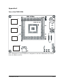
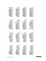
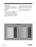
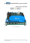
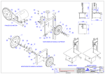
_ V1.4 User’s Manual EVB-5554 Evaluation & Development Kit for Freescale PowerPC MPC5554 Microcontroller Ordering code EVB-5554 ITMPC5554 Copyright 2007 iSYSTEM AG. All rights reserved. winIDEA is a trademark of iSYSTEM AG. All other trademarks used in this document are property of their respective owners. www.isystem.com iSYSTEM, July 2007 1/16 Contents Contents ................................................................................................................................. 2 Features.................................................................................................................................. 3 Specifications ...................................................................................................................... 3 EVB-5554 Features ............................................................................................................ 3 Software Development........................................................................................................ 3 Getting Started - Setting up the EVB-5554 Board............................................................... 3 Power Supply ...................................................................................................................... 3 Use of On-Board Integrated Debugger ............................................................................... 4 What To Do Now?............................................................................................................... 4 Troubleshooting .................................................................................................................. 5 EVB-5554 doesn’t show signs of life by first start........................................................................................... 5 Unable to download the code to the board...................................................................................................... 5 Checksum failed error ..................................................................................................................................... 5 Default Memory Map.............................................................................................................. 5 EVB-5554 Memory Map...................................................................................................... 6 Internal Memory.............................................................................................................................................. 6 External Memory ............................................................................................................................................. 6 SRAM Memory.................................................................................................................... 6 Flash Memory ..................................................................................................................... 6 Downloading the code into the memory.............................................................................. 6 Settings and Options............................................................................................................. 7 Jumpers .............................................................................................................................. 7 Status Indicators ................................................................................................................. 8 Component List................................................................................................................... 8 Connectors.......................................................................................................................... 8 14-pin JTAG debug connector (ONCE) .......................................................................................................... 8 Nexus 38-pin Mictor debug connector ............................................................................................................ 9 CPU expansion connector ............................................................................................................................... 9 Appendix A........................................................................................................................... 10 View of the ITMPC5554 .................................................................................................... 10 Schematic ......................................................................................................................... 12 iSYSTEM, July 2007 2/16 Features The ITMPC5554 Target Board is an evaluation and a development system for the Freescale MPC5554 microcontroller. The ITMPC5554 package consists of a USB cable, a power supply and a target board populated with the Freescale MPC5554 CPU, 2 MB SRAM (4 devices 128Kx32-bit), JTAG debug and Nexus debug connectors and an on-board integrated iSYSTEM JTAG debugger. The application under the development or test can run from the internal CPU flash or from the external SRAM. Specifications Clock Speed – up to 132 MHz Power requirement: 6 - 12V DC , + in the center @ 500 mA Power output: 5V, 3.3V, and 2.5V regulated supplies Board Size: 131 mm x 110 mm EVB-5554 Features x x x x x x x x MPC5554 Ext. 2Mbit (ҏ4 devices 128K x 32-bit) SRAM (CY7C1338F) 8MHz clock (ext. crystal) Power Indicators – Supply voltage indications for 5V, 3.3V, and 2.5V supplies User Indicator – two user indicators to provide user conceived visual response during testing Configuration jumper - Jumpers J1 to J5 configures processor startup mode; Jumper J6 enables/disables the iSYSTEM on-board integrated USB-JTAG debugger Two debug options available – JTAG, Nexus Low cost and user friendly support manual and software Software Development The board has been tested and does run at speeds up to 132 MHz, which you can set by engaging the PLL module in your software. Software development on the EVB-5554 can be performed using the iSYSTEM on-board integrated USB-JTAG debugger. Alternatively, external development tools can be connected to the ONCE (JTAG) or P2 (Nexus) connector. This provides real-time access to all hardware, peripherals and memory on the board. Software is usually uploaded to the external SRAM where it’s executed during the development. Then it can be programmed into the CPU Flash in order to execute in standalone when the power is applied. Getting Started - Setting up the EVB-5554 Board Power Supply Permissible input voltage: 6-12 V DC, + in the center. The required current load capacity of the power supply depends on the specific configuration of the ITMPC5554. A power supply with a minimum of 500mA is recommended and delivered in the package. Low voltage DC plug must conform to the DIN 45323 standards: x x The hole diameter is 1.95 – 2.5 mm (standard: 2.1 mm) The external diameter is 6.2 - 5.5 mm (standard: 5.5 mm) Switch-on the EVB-5554 after the AC adapter is plugged into the wall and connected to the EVB5554. Check that power indicators (LD11, LD12, LD13) lit, indicating that 5V, 3.3V and 2.5V voltage is present. iSYSTEM, July 2007 3/16 Note: When connecting an external debugger, make sure that the emulator is powered on first, then the target board and vice versa when switching off the system. First, switch off the target and then the emulator. Use of On-Board Integrated Debugger Follow below instructions, in order to get a sample application running with “out of the box” experience. If winIDEA 2007 CD is not part of the package, please obtain winIDEA 2007 setup from your local iSYSTEM office or from www.isystem.com. x x x x x x x x x x x Install winIDEA 2007 (IDE) full setup on a PC. Set jumpers J1-J5 in their default position. Set jumper J6, which enables on-board integrated debugger. Make sure that power switch on the ITMPC5554 is in off position. Connect the power supply to the ITMPC5554. Switch on the ITMPC5554. Run winIDEA by selecting Start>Programs>… and open ITMPC5554 sample workspace (.jrf) running from the internal flash c:\winIDEA\2007\Examples\Targets\ITMPC5554\IntFLASH). Connect USB cable between the PC and the ITMPC5554. Windows should auto-detect a new USB device and install belonging USB driver. In case of any problems, the driver is located under winIDEA install directory (e.g. c:\winIDEA\2007\USBDrv). Execute Debug/Download. This should program and run the application until main function. The application is now ready for debugging. If you run the application, a successful operation is indicated with blinking LED LD11 and LD12. The on-board integrated USB-JTAG debugger runs without restrictions for 90 days after using it for the first time. After the 90 day period expires, the debugger falls back to a restriction of a 32k byte download limit. The debugger can be upgraded to a regular debugger (no limits) by purchasing the debug enable license. Additionally, you need to purchase a regular winIDEA license. Please contact your local iSYSTEM distributor for more details on upgrading your development tool. What To Do Now? winIDEA allows you to run code step by step, set execution and access breakpoints, examine and modify the source code, rebuild the project using GNU compiler, which is optionally installed during winIDEA installation, and much more. For more information refer to the winIDEA documentation. Software in the combination with the development board can be used as a basis for developing future applications also on your hardware. This project illustrates various programming issues, which are essential to all winIDEA projects: x x x x x Initialization of bus interface unit Initialization of configuration registers Implementation of dispatch table Format of linker definition file Correct project settings (Project>Settings), which ensure that the compiler is invoked successfully More interesting examples are also included on the support CD. iSYSTEM, July 2007 4/16 Troubleshooting EVB-5554 doesn’t show signs of life by first start a) Check the power supplied to the EVB board – Diodes LD11, LD12 and LD13. b) When using the on-board integrated JTAG debugger, make sure that Jumper J6 is enabled. When Jumper J6 is not enabled, a connection to the JTAG or Nexus port must be made. c) Try “slow” JTAG Scan Speed if the debugger cannot connect to the CPU. d) Execute debug Reset instead of debug Download. Unable to download the code to the board a) Check the power supplied to the EVB board. b) Ensure that the correct workspace was loaded into winIDEA. c) Check the hardware configuration: x Tools>Hardware Plug-In x Hardware>Hardware … x Hardware>Emulation Options d) Reset the board and try to connect again. Checksum failed error a) When performing any kind of checksum, remove all software breakpoints Default Memory Map The MPC5554 of the MPC5500 family has two levels of memory hierarchy. The fastest accesses are to the unified 32 Kbytes cache. The next level in the hierarchy contains the 96-Kbyte internal SRAM and internal 2MB Flash memory. Both the internal SRAM and the Flash memory can hold instructions and data. The external bus interface has been designed to support most of the standard memories used with the MPC55xx family. The provided software uses the default memory map. If you modify the memory map make sure that all memory banks and chip select configuration settings are adjusted accordingly. iSYSTEM, July 2007 5/16 EVB-5554 Memory Map Internal Memory Address Range Memory Type Description 0x 0000 00000x 001F FFFF 2MB - Internal Flash Memory Internal Flash memory (512KB – 2MB) 0x 2000 00000x 3FFF FFFF 512MB - External Memory External Memory (see note below) 0x C3F0 00000x C3F0 3FFF Bridge A Peripherals Acts as an interface between the system bus and the lower bandwidth peripherals 0x FFF0 00000x FFFF FFFF Bridge B Peripherals Acts as an interface between the system bus and the lower bandwidth peripherals 0x 4000 00000x 4000 7FFF Internal SRAM, Powered Standby 32 Kbytes 0x 4000 80000x 4000 FFFF Internal SRAM 32 Kbytes External Memory There are 4 SRAM devices connected to CS1 and CS2 and cover a 2MB memory area. Offset depends on the CPU configuration. In our case, CS1 is configured to point at 0x2000 0000 through the winIDEA initialization sequence. Address Range 0x 2000 0000 – 0x 2007 FFFF 0x 2008 0000 – 0x 200F FFFF 0x 2010 0000 – 0x 2017 FFFF 0x 2018 0000 – 0x 201F FFFF SRAM Memory The MPC5554 internal SRAM module provides a general-purpose 96-Kbyte memory block that supports mapped read/write accesses from any master. Included within the 96-Kbyte SRAM block is a 32-Kbyte block powered by a separate supply for a standby operation. Flash Memory The MPC5554 provides 2 Mbytes of programmable, non-volatile, Flash memory storage. The nonvolatile memory (NVM) can be used for instruction and/or data storage. Downloading the code into the memory winIDEA allows you to load the code directly into the internal Flash memory through the standard debug download. winIDEA identifies, which code from the download file fits in the internal FLASH, and loads it to the Flash through the flash programming procedure hidden to the user. All other code propagates to the target through standard memory writes. iSYSTEM, July 2007 6/16 Demo software has the example configured for the internal Flash. Load the project into winIDEA and execute debug download (Debug->Download), which will download the code directly to the Flash memory. For more information see the winIDEA users manual. Demo software has also the example configured for the external SRAM. Load the project into winIDEA and execute debug download (Debug->Download), which will download the code to the external SRAM. Access to the external SRAM is configured in the initialization sequence (‘Hardware/Emulation Options/Initialization’ tab), which winIDEA executes prior to debug download. Settings and Options Jumpers Jumpers J1 to J5 configures processor startup mode. See MPC5554 Reference Manual for more details on the CPU signals BOOTCFG[0:1], PLLCFG[0:1] and WKPCFG. Some boards may not have J1-J5 populated since the CPU has internal pull-ups/downs on belonging signals, which match with the default jumper settings. Jumper J6 selects whether iSYSTEM on-board integrated USB-JTAG debugger is used or an external debug tool. Jumper pin 1 is marked with a white square on the ITMPC5554 PCB. If pin 1 cannot be located directly from the ITMPC5554, please use Figure 2 for assistance. Note: Don’t change jumper settings while the ITMPC5554 Target Board is supplied with power! J1 1-2* 2-3 BOOTCFG0 BOOTCFG0 = 0 BOOTCFG0 = 1 J2 1-2* 2-3 BOOTCFG1 BOOTCFG1 = 0 BOOTCFG1 = 1 J3 1-2 2-3* PLLCFG0 PLLCFG0 = 0 PLLCFG0 = 1 J4 1-2 2-3* PLLCFG1 PLLCFG1 = 0 PLLCFG1 = 1 J5 1-2 2-3* WKPCFG WKPCFG = 0 WKPCFG = 1 J6 Closed* Open Debug mode Enable integrated USB-JTAG debugger External debugger Figure 1: Jumper configuration (* - default position) iSYSTEM, July 2007 7/16 Status Indicators Three LED diodes show the presence of supply voltages. LD11 (+5V), LD12 (+3.3V) and LD13 (+2.5V) must light when the power is applied to the evaluation board. LD14 and LD15 are available for the user as a status indicator. Component List Name U22 U1,U8,U9,U10 P1(bottom) P2 P4 ONCE J1 J2 J3 J4 J5 J6 J28 LD11 LD12 LD13 LD14 LD15 SW1 Description Motorola MPC5554 CPU SRAM Cypress CY7C1338F Connector for manufacturing purpose Nexus debug connector Power supply connector JTAG debug connector BOOTCFG0 BOOTCFG1 PLLCFG0 PLLCFG1 WKPCFG Debug mode USB connector (integrated debugger) Power LED 5V Power LED 3,3V Power LED 2,5V User LED User LED Power switch Connectors 14-pin JTAG debug connector (ONCE) CPU_TDI 1 2 GND CPU_TDO 3 4 GND CPU_TCK 5 6 GND N.C. 7 8 N.C. CPU_RESET 9 10 CPU_TMS 3V3 11 12 N.C. N.C. 13 14 CPU_TRST External JTAG debug tool connects to a 14-pin JTAG debug connector. Jumper J6 must be open when using external debugger. iSYSTEM, July 2007 8/16 Nexus 38-pin Mictor debug connector Signal Not used Not used MDO9 BOOTCFG RSTIN TDO MDO10 TCK TMS TDI NTRST MDO11 Not used Not used Not used Not used Not used Not used Not used Pin 1 3 5 7 9 11 13 15 17 19 21 23 25 27 29 31 33 35 37 Pin 2 4 6 8 10 12 14 16 18 20 22 24 26 28 30 32 34 36 38 Signal Not used Not used CLKOUT MDO8 EVTIN VTREF RDY MDO7 MDO6 MDO5 MDO4 MDO3 MDO2 MDO1 MDO0 EVTO MCKO MSEO1 MSEO0 External Nexus debug tool connects to a Nexus 38-pin Mictor debug connector. Jumper J6 must be open when using external debugger. CPU expansion connector The CPU expansion connector makes all the CPU signals accessible and can be used in order to expand the development system by connecting the ITMPC5554 to another module. The CPU expansion connector uses the same numbering scheme as the original CPU in the PBGA416 package. The CPU expansion connector builds the matrix that matches with the CPU PBGA416 pinout. iSYSTEM, July 2007 9/16 Appendix A View of the ITMPC5554 U1 U8 U9 U10 Note: A designation on Figure 4 stands for A1 designation on the above ITMPC5554 view, B stands for B1, AF stands for AF1 etc. iSYSTEM, July 2007 10/16 Figure 4: Expansion connector iSYSTEM, July 2007 11/16 Schematic Note: On-board integrated JTAG debugger is not part of the schematic. iSYSTEM, July 2007 12/16 iSYSTEM, July 2007 13/16 iSYSTEM, July 2007 14/16 iSYSTEM, July 2007 15/16 Disclaimer: iSYSTEM assumes no responsibility for any errors which may appear in this document, reserves the right to change devices or specifications detailed herein at any time without notice, and does not make any commitment to update the information herein. ¤ iSYSTEM. All rights reserved. iSYSTEM, July 2007 16/16