1
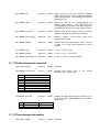
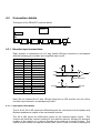
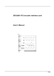
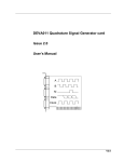
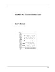
DEVA037 USB encoder interface card with
optical edge detection
User’s Manual
A
B
M
P
O
V1.0
52 Woodside Business Park
Birkenhead
Wirral CH41 1EL
United Kingdom
Tel +44 (0)151 647 3222
Fax +44 (0)151 647 4511
Email: [email protected]
Web: www.deva.co.uk
All information of a technical nature and particulars of the product and its use are given by
Deva Electronic Controls Ltd. in good faith. However, it is acknowledged that there may be
errors and omissions in this manual. We shall not be liable for loss or damage whatsoever
arising from the use of any information or particulars in, or any omissions from, this document.
V1.0
DEVA001 PCI User’s Manual
Overview
1
Overview ........................................................................1
1.1
Product Features..................................................................... 1
1.1.1 Features...................................................................................................... 1
1.2
Support software..................................................................... 1
1.2.1 Windows 8/7/Vista/XP 32/64 ..................................................................... 1
1.2.2 Digital Readout .......................................................................................... 2
1.3
Accessories ............................................................................. 2
2
Installation and configuration ......................................3
2.1
Software support CDROM ...................................................... 3
2.2
USB Plug and Play cards ........................................................ 3
2.2.1 System requirements ................................................................................ 3
2.2.2 Device driver installation .......................................................................... 4
3
Device Driver Usage......................................................5
3.1
Device driver functions........................................................... 5
3.1.1 System information ................................................................................... 5
3.1.2 Channel information.................................................................................. 5
3.1.3 Marker information.................................................................................... 7
3.1.4 Zero information ........................................................................................ 8
3.1.5 Extended axes ........................................................................................... 8
3.1.6 Input status ................................................................................................ 9
3.1.7 Timer information...................................................................................... 9
3.1.8 DAC Control ............................................................................................. 10
3.1.9 Output control.......................................................................................... 10
3.1.10 Probe information.................................................................................... 10
3.1.11 Probe information extended................................................................... 11
3.1.12 Time-stamper information ...................................................................... 11
3.1.13 Pulse generator information................................................................... 12
3.1.14 Axis compare information ...................................................................... 13
3.1.15 User event information ........................................................................... 13
3.1.16 Input event information........................................................................... 13
i
Overview
DEVA001 PCI User’s Manual
3.1.17 Digital I/O information............................................................................. 15
3.1.18 FIFO buffer information .......................................................................... 15
3.1.19 Software call-back information.............................................................. 17
3.1.20 Optical edge detector.............................................................................. 17
3.2
Function compatibility .......................................................... 19
3.3
Device driver programming from ‘C’ ................................... 22
3.3.1
3.3.2
3.3.3
3.3.4
3.3.5
3.3.6
short open_encoder (void) ..................................................................... 22
void close_encoder (void) ...................................................................... 22
long read_encoder (short command, short channel) .......................... 22
void write_encoder (short command, short channel, long value)...... 22
short enclib_callback (short receive, long priority);............................ 23
Example 'C' programming...................................................................... 24
3.4
Device driver programming from Visual Basic ................... 25
3.4.1 Function open_encoder () As Integer.................................................... 25
3.4.2 Function close_encoder () As Integer ................................................... 25
3.4.3 Function read_encoder (ByVal com As Integer, ByVal chan As
Integer) As Long...................................................................................... 25
3.4.4 Function write_encoder (ByVal com As Integer, ByVal chan As
Integer, ByVal value As Long) As Integer ............................................. 25
3.4.5 Example Visual Basic programming..................................................... 26
3.5
Device driver programming from C# .Net............................ 28
3.5.1
3.5.2
3.5.3
3.5.4
public static short open_encoder() ....................................................... 28
public static void close_encoder() ........................................................ 28
public static int read_encoder(short command, short channel) ........ 28
public static void write_encoder(short command, short channel, int
value) ........................................................................................................ 28
3.5.5 Example C# programming ..................................................................... 29
4
USB incremental encoder interface hardware ......... 30
4.1
Functional description.......................................................... 30
4.1.1 Quadrature input ..................................................................................... 30
4.1.2 Marker input............................................................................................. 30
4.1.3 Zero input................................................................................................. 30
ii
DEVA001 PCI User’s Manual
Overview
4.1.4 Touch Probe Interface............................................................................. 31
4.2
Optical edge detector input. ................................................. 31
4.3
Connection details ................................................................ 32
4.3.1
4.3.2
4.3.3
4.3.4
4.3.5
Encoder input connections .................................................................... 32
Touch probe input connections ............................................................. 33
USB connection....................................................................................... 33
Internal Encoder Power .......................................................................... 34
Optical ...................................................................................................... 34
iii
1
Overview
1.1
Product Features
The DEVA037 3 axis incremental encoder interface cards have been designed to
enable simultaneous reading of 3 encoders using a PC based system. They can be
used for a wide range of measurement applications, such as optical projectors and
co-ordinate measuring machines.
The range includes support for PCIe, PCI and ISA bus interfaces. All three types
share many common features; however the PCI / PCIe variants have several
additional facilities.
1.1.1 Features
1.2
•
Three encoder inputs for differential or single - ended input
•
32 bit counters for each encoder channel
•
Marker input (freeze / capture) for each encoder channel
•
+5v and +12v Power supply pass through on encoder connectors
•
Digital filters on all channels
•
Timer / Event driven interrupt logic
•
Touch probe input
•
Optical edge input
Support software
A variety of software drivers and libraries are provided with the interface card to
enable software development to be performed within a number of operating systems
and applications. Software support is an ongoing activity, if support for a particular
application or operating system is not currently provided, please call the Deva office
to determine its availability.
1.2.1 Windows 8/7/Vista/XP 32/64
The Deva037 is supported in Windows 8/7/Vista/XP 32/64 by a Windows driver
model driver (WDM). The driver supports a standard programming interface. Please
refer to section 3 ‘Device Driver Usage’ for more details.
1.2.2 Digital Readout
A powerful digital readout is supplied which is capable of exercising all the common
facilities of the DEVA037. This is useful to allow users to quickly verify that the
DEVA037 is installed correctly and to make checks of their system without having to
write their own software.
The DRO will handle up to four cards (12 axes) and displays both absolute and
incremental positions. The DRO also displays the Marker register, Probe register
and allows control of the Probe and Footswitch options.
To allow the user to read meaningful values each axis of the DRO may be
independently scaled to display real units.
For the incremental card all facilities such as Marker, Probe and Optical edge detect
may be toggled on and off. If a Probe is activated the probed values are shown in
the Probe register, if a Marker is activated the value is shown in the Marker register
an if the Optical edge is activated the values are shown in the Optical register.
1.3
Accessories
The DEVA037 incremental encoder interface is supplied with three high density 15
way 'D' type connectors, one 9 way ‘D’ type connector and matching shells.
2
Installation and configuration
2.1
Software support CDROM
The DEVA037 3-axis encoder interface card is supplied with a software support
CDROM containing support for all DEVA037 encoder interfaces along with support
and information for many of Deva’s other products. The CDROM includes the
following items:
· Windows 8/7/Vista/XP 32/64 bit device drivers, providing coherent encoder
interface card hardware management.
· Windows 8/7/Vista/XP 32/64 bit DLL and import library, containing the driver
access functions.
· 'C' language library routines and header files, which create a simple interface to
device driver functions.
· Example 'C' programs, illustrating card read/write using device driver functions.
· Visual Basic 6 Module, which provides constant and function definitions to allow
simple DLL access.
· Example Visual Basic 6 programs, illustrating card read/write using device driver
functions.
· .Net 2.0 Assembly, which provides a complete interface to the standard DLL.
· Example C# programs, illustrating card read/write using device driver functions.
· Demonstration Digital Readout Program for Windows 8/7/Vista/XP 32 and 64 bit.
2.2
USB Plug and Play cards
2.2.1 System requirements
The device driver library functions and the demonstration software require a PC
computer with one spare USB connector and Windows 8/7/Vista or XP 32/64 bit
operating systems. Both 32 and 64 bit operating systems are fully supported.
2.2.2 Device driver installation
2.2.2.1 Windows 8 / 7 / Vista / XP installation
When the card is connected windows will indicate that a new device has been found
and will start the standard driver installation procedure. If this does not occur it is
possible to initiate this process manually via the ‘add new hardware’ icon in the
control panel or via the windows device manager.
Follow the instructions and when requested select ‘have disk’ and then browse to the
directory on the installation CDROM containing the Deva037.inf file.
For example :
\PC interface products\Deva037\Issue1.x\Drivers\
Click ok and follow instructions to complete the installation.
The installation may be tested using the supplied DRO program which may be found
on the CD in the utils\Win32 or utils\Win64 directories.
3
Device Driver Usage
3.1
Device driver functions
The supplied Windows 8/7/Vista/XP 32/64 bit device drivers provide a simple method
of accessing card functions and remove the need for direct register programming.
Use of the device driver ensures that the user's application software is compatible
with other Deva products and is protected from any future changes in the card
hardware or register layout. The device driver determines the total number of axes
and I/O available from all the cards in a system. This section describes the functions
provided by the device driver whilst the compatibility chart in section 3.2 details the
functions available from particular cards.
3.1.1 System information
Command & equate
Channel
Rd/Wr
Operation
0
VECTOR
Not used
Rd
Provides a vector to the device driver command
handler.
1
NUM_AXES
Not used
Rd
Returns the total number of axis channels
available from the installed cards.
2
NUM_TIMERS
Not used
Rd
Returns the total number of timers available from
the installed cards.
3
NUM_INPUTS
Not used
Rd
Returns the total number of digital inputs available
from the installed cards.
4. NUM_DACS
Not used
Rd
Returns the total number of digital to analog
converters available from the installed cards.
5. NUM_OUTPUTS
Not used
Rd
Returns the total number of digital outputs
available from the installed cards.
7. NUM_BOARDS
Not used
Rd
Returns the number of encoder cards present in
the system.
8. CARD_TYPE
Not used
Rd
Returns the card type identifier.
9. VERSION_NUM
Not used
Rd
Returns the device
multiplied by 100.
Command & equate
Channel
Rd/Wr
Operation
10 CNT_16
Axis no.
Rd/Wr
Allows direct 16 bit read/write of the counter chip
registers.
driver
version
number
3.1.2 Channel information
11 MODE
Axis no.
Rd/Wr
INC_MODE
Bit
0-3
4
5
6
7
8
9
Allows access to the mode registers of the
incremental encoder counter chip or the SSI mode
register.
Incremental mode number formed from a variety
of bit fields.
Function
Count mode:
5=QUADx4AB, quadrature AB decode (default)
8=CNTAx2DIRB, count rising and falling edges of A, B selects count up/down direction
9=CNTADIRB, count rising edges of A, B selects count up/down direction
Invert quadrature signal A
Invert quadrature signal B
Invert marker signal M
Invert zero signal Z
Disable marker synchronisation with signals A & B
Count inhibit
SSI_MODE
Bit
0-2 (ISA)
0-2 (PCI)
3-7
8-11
12-13
14
15
16-18
18-22
23
24-29
30-31
SSI mode number formed from a variety of bit
fields.
Function
Frequency 0=2.50Mhz, 1=1.25Mhz, 2=625kHz, 3=313kHz, 4=156kHz, 5-7=78.1kHz
Frequency 0=2.78Mhz, 1=1.39Mhz, 2=694kHz, 3=347kHz, 4=174kHz, 5-7=86.8kHz
Reserved
Offset 0 to 15 bits
Extra bit, 0=None, 1=Power fail, 2=Even Parity, 3=Odd parity
0=Binary, 1=Gray
Output control, 0=Off, 1=On
Acquisition mode, 0=One Shot, 1=Timer, 2-3=Continuous, 4=Channel Digital Input 0
Reserved
Read Complete Interrupt Enable, 0=Off (Default), 1=On
Data length 1 to 32
Reserved
12 AXIS_SIZE
Axis no.
Rd
Returns the number of 16 bit registers allocated to
an input channel.
13 ENCODER_TYPE
Axis no.
Rd
0 = Incremental, 1 = SSI
14 AXIS_INPUTS
Axis no.
Rd
Returns the status of the axis (post filter &
inverter) inputs. The bit fields indicate 0 or 1
depending on the state of the axis inputs.
INC_INPUTS
Bit
0
1
2
3
4
5
Status
Quadrature input A
Quadrature input B
Marker input M
Zero input Z
Limit input 0
Limit input 1
Incremental inputs register formed from a variety
of bit fields.
SSI_INPUTS
Bit
0
SSI inputs register formed from a variety of bit
fields.
Status
Raw SSI data input
15 AXIS_STATUS
Axis no.
Rd
INC_STATUS
Bit
0
1
Incremental status register formed from a variety
of bit fields.
Status
Power supply failure
Quadrature error
SSI_STATUS
Bit
0
1
2
Returns the axis status register. The bit fields
indicate 0 or 1 depending on the status bit.
SSI status register formed from a variety of bit
fields.
Status
Power supply failure
Parity failure
Read complete occur
16 AXIS_OUT_EN
Axis no.
Rd
Enables the axis digital outputs. Specifying 1/0 in
each bit field enables/disables the equivalent
digital output.
INC_OUT_EN
N/A
SSI_OUT_EN
SSI axis digital output enable register formed from
a variety of bit fields.
Bit
0
1
Status
SSI Read Trigger
SSI Read Complete
3.1.3 Marker information
Command & equate
Channel
Rd/Wr
Operation
20 MARK_16
Axis no.
Rd
Returns the value of a 16-bit counter register
latched by the last marker function (or any other
function the marker latch source is set to). See
commands 23 and 26.
21 MARK_INPUT
Axis no.
Rd
Returns either 0 or 1 depending on the state of the
marker input.
22 MARK_INT
Axis no.
Rd/Wr
Allows access to the card interrupt controller
mask. Writing a value of 1/0 enables/disables an
interrupt from the marker input. This function is
for special applications only.
23 MARK_FUNC
Axis no.
Rd/Wr
Writing a value of 1/0 enables/disables the
channel marker function.
24 MARK_INT_VECT
Axis no.
Rd/Wr
Allows access to the interrupt vector or interrupt
call-back executed by a marker input interrupt.
25 MARK_INT_OCCUR
Axis no.
Rd
Returns a value of 1 every time a marker input
interrupt has occurred.
26 MARK_LATCH_SEL
Axis no.
Rd/Wr
Controls the source event
associated latch of each axis.
Axis no.
Rd/Wr
Writing a value of 1/0 enables/disables the marker
digital output.
Command & equate
Channel
Rd/Wr
Operation
30 ZERO_INPUT
Axis no.
Rd
Returns either 0 or 1 depending on the state of the
zero input.
31 ZERO_INT
Axis no.
Rd/Wr
Allows access to the card interrupt controller
mask. Writing a value of 1/0 enables/disables an
interrupt from the zero input. This function is for
special applications only.
32 ZERO_FUNC
Axis no.
Rd/Wr
Writing a value of 1/0 enables/disables the
channel zero function.
33 ZERO_INT_VECT
Axis no.
Rd/Wr
Allows access to the interrupt vector or interrupt
call-back executed by a zero input interrupt.
34 ZERO_INT_OCCUR
Axis no.
Rd
Returns a value of 1 every time an encoder zero
interrupt has occurred.
Command & equate
Channel
Rd/Wr
Operation
40 AXIS_32
Axis no.
Rd/Wr
Allows access to the 32-bit counter register values
or to pseudo-incremental 32-bit position for
absolute SSI encoders.
Value
0
1
2
3
4
5
6
7
of
the
‘Marker’
Source
Marker Occur
Zero Occur
Pulse Generator 0 Sync Occur
User Event 0 Occur
Channel Digital Input 0 Occur
Axis Compare 0 Sync Occur
Axis Compare 1 Sync Occur
N/A (Axis Compare 0 Enable)
27 MARK_OUT_EN
3.1.4 Zero information
3.1.5 Extended axes
41 MARK_32
Axis no.
Rd
Returns the value of a 32-bit counter register
latched by the last marker function (or any other
function the marker latch source is set to). See
commands 23 and 26.
42 VEL_INST
Axis no.
Rd
Returns the counter velocity per interrupt time.
43 VEL_FILT
Axis no.
Rd
Returns 10 times the counter velocity per interrupt
period filtered over 10 samples.
44 ACCEL_INST
Axis no.
Rd
Returns the counter acceleration per interrupt
time.
45 ACCEL_FILT
Axis no.
Rd
Returns 102 times the counter acceleration per
interrupt period2 filtered over 10 samples.
46 PROBE_32
Axis no.
Rd
Returns the value of a 32-bit counter register
latched by the last probe function (or any other
function the probe latch source is set to). See
commands 93 and 100.
47 ABSOLUTE_32
Axis no.
Rd
Returns the 32-bit absolute position latched by the
last read of an absolute SSI encoder.
48 TIMER_32
Axis no.
Rd
Returns the value of a 32-bit counter value latched
by the last timer 1 function (or any other function
the timer latch source is set to). See commands
65 and 64.
49 OPTICAL_32
Axis no.
Rd
Returns the 32 bit latched encoder value of the
last optical trigger.
Command & equate
Channel
Rd/Wr
Operation
50 INPUT
Input no.
Rd
Returns either 0 or 1 depending on the state of the
input.
Command & equate
Channel
Rd/Wr
Operation
60 TIMER
Timer no.
Rd/Wr
This command allows access to the interval
values of the on-board user timers. The timer
intervals are programmed in units of 0.1 ms.
61 TIMER_INT
Timer no.
Rd/Wr
Writing a value of 1/0 enables/disables the user
timer interrupt.
62 TIMER_INT_VECT
Timer no.
Rd/Wr
Allows access to the interrupt vector or interrupt
call-back executed by the user timer interrupt.
63 TIMER_INT_OCCUR
Timer no.
Rd
Returns a value of 1 every time a user timer
interrupt has occurred.
64 TIMER_LATCH_SEL
Axis no.
Rd/Wr
Controls the source event of the timer latch of
each axis.
3.1.6 Input status
3.1.7 Timer information
Value
0
1
2
3
Source
Timer 1 Sync Occur
N/A (Read Counter)
Pulse Generator 0 Sync Occur
User Event 0 Occur
65 TIMER1_FUNC
Axis no.
Rd/Wr
Writing a value of 1/0 enables/disables the user
timer function for the specific axis. This allows for
position readings latched on every timer 1 interval
of the equivalent board.
66 TIMER_OUT_EN
Timer no.
Rd/Wr
Enables the timer digital outputs. Specifying 1/0 in
each bit field enables/disables the equivalent
digital output.
Bit
Status
0 Timer Occur
1 Timer Terminal Count
Pulse Width
Occur to serviced
1us
3.1.8 DAC Control
Command & equate
Channel
Rd/Wr
Operation
70 DAC_MV
Axis no.
Rd/Wr
Allows access to the analog output channel for
each axis in a system. The value is in units of mV.
71 DAC_UV
Axis no.
Rd/Wr
Allows access to the analog output channel for
each axis in a system. The value is in units of uV.
Command & equate
Channel
Rd/Wr
Operation
80 OUTPUT
Output no. Rd/Wr
Allows access to the system digital outputs. The
output is energised with a logical 1.
81 SERVO_ENABLE
Axis no.
Rd/Wr
Allows access to the system servo enable outputs
for each axis. The output is energised with a
logical 1.
Command & equate
Channel
Rd/Wr
Operation
90 PROBE_16
Axis no.
Rd
Returns the value of a 16-bit counter register
latched by the last probe function (or any other
function the probe latch source is set to). See
commands 93 and 100.
91 PROBE_INPUT
Board no.
Rd
Returns either 0 or 1 depending on the state of the
probe input.
3.1.9 Output control
3.1.10 Probe information
92 PROBE_INT
Board no.
Rd/Wr
Allows access to the card interrupt controller
mask. Writing a value of 1/0 enables/disables the
probe input interrupt. This function is for special
applications only.
93 PROBE_FUNC
Board no.
Rd/Wr
Writing a value of 1/0 enables/disables the
channel probe function. The probe function is
level triggered by the probe input and the function
reset automatically after execution of the function.
94 PROBE_INT_VECT
Board no.
Rd/Wr
Allows access to the interrupt vector or interrupt
call-back executed by a probe input interrupt.
95 PROBE_INT_OCCUR
Board no.
Rd
Returns a value of 1 every time a probe input
interrupt has occurred.
96 PROBE_SENSE
Board no.
Rd/Wr
Allows access to the probe sense control. Writing
a value of 0/1 sets probe operation to active
high/low.
97 PROBE_LED
Board no.
Rd/Wr
0 = Off, 1 =On, 2 = Auto
98 PROBE_SOUND
Board no.
Rd/Wr
0 = Off, 1 =On, n = time in ms
99 PROBE_FOOTSWITCH
Board no.
Rd/Wr
0 = Off, 1 = Auto, 2 = Auto (Inverted)
3.1.11 Probe information extended
Command & equate
Channel
Rd/Wr
Operation
100 PROBE_LATCH_SEL
Axis no.
Rd/Wr
Controls the source event
associated latch of each axis.
Rd/Wr
Enables the probe digital outputs. Specifying 1/0
in each bit field enables/disables the equivalent
digital output.
Value
0
1
2
3
4
5
6
7
of
the
‘Probe’
Source
Probe Occur
N/A (Read Counter)
Pulse Generator 0 Sync Occur
User Event 0 Occur
Channel Digital Input 0 Occur
Axis Compare 0 Sync Occur
Axis Compare 1 Sync Occur
N/A (Axis Compare 1 Enable)
101 PROBE_OUT_EN
Bit
Status
0 Probe Occur
1 Footswitch Occur
Board no.
Pulse Width
Occur to serviced
Occur to serviced
3.1.12 Time-stamper information
Command & equate
Channel
Rd/Wr
Operation
110 TIMESTAMP_NOW
Board no.
Rd/Wr
Allows access to the current value of the 32-bit
time-stamper register in units of 1μs.
111 TIMESTAMP_EVENT
Board no.
Rd
Allows access to the latched value of the 32-bit
time-stamper register in units of 1μs.
112 TIMESTAMP_SEL
Board no.
Rd/Wr
Controls the source event of the Time-stamper
latch.
Value
0
1
2
3
4
5
6
7
Source
Probe Occur
Timer 1 Sync Occur
User Event 0 Occur
Board Digital Input 0 Occur
Pulse Generator 0 Sync Occur
Axis Compare 0 Sync Occur
Axis Compare 1 Sync Occur
Reserved
3.1.13 Pulse generator information
Command & equate
Channel
Rd/Wr
Operation
120 PULSEGEN0
Axis no.
Rd/Wr
Allows access to the 16-bit pulse generator
register in units of 1 quadrature count.
121 PULSEGEN0_MODE
Axis no.
Rd/Wr
Controls the mode of operation of the pulse
generator.
Bit
0
1
2
3
Function
Direction when in Uni-directional mode (1/0 = +/-)
Bi-directional operation (1/0 = Bi-directional / Uni-directional)
Hardware Start/Stop by Axis Comparators (1/0 = On/Off)
Deglitch - Do not repeat the same pulse sequentially (1/0 = On/Off)
122 PULSEGEN0_EN
Axis no.
Rd/Wr
Writing a value of 1/0 enables/disables the pulse
generator function.
123 PULSEGEN0_OCCUR
Axis no.
Rd
Returns a value of 1 every time a pulse generator
interrupt has occurred.
124 PULSEGEN0_OUT_EN
Axis no.
Rd/Wr
Enables the pulse generator 0 digital outputs.
Specifying 1/0 in each bit field enables/disables
the equivalent digital output.
Bit
Status
0 Pulse Generator 0 Occur
1 Pulse Generator 0 Terminal Count
125 PULSEGEN0_INT_VECT Axis no.
Pulse Width
Occur to serviced
Quadrature count width
Rd/Wr
Allows access to the interrupt vector or interrupt
call-back executed by a pulse generator 0
interrupt.
3.1.14 Axis compare information
Command & equate
Channel
Rd/Wr
Operation
130 COMPARE0
Axis no.
Rd/Wr
Allows access to the 32-bit axis compare 0
register.
131 COMPARE0_FUNC
Axis no.
Rd/Wr
Writing a value of 1/0 enables/disables the axis
compare 0 function.
132 COMPARE0_OCCUR
Axis no.
Rd
Returns a value of 1 every time an axis position
compare 0 has occurred.
133 COMPARE0_OUT_EN
Axis no.
Rd/Wr
Writing a value of 1/0 enables/disables the axis
compare 0 digital output.
134 COMPARE0_INT_VECT
Axis no.
Rd/Wr
Allows access to the interrupt vector or interrupt
call-back executed by an axis compare 0 interrupt.
135 COMPARE1
Axis no.
Rd/Wr
Allows access to the 32-bit axis compare 1
register.
136 COMPARE1_FUNC
Axis no.
Rd/Wr
Writing a value of 1/0 enables/disables the axis
compare 1 function.
137 COMPARE1_OCCUR
Axis no.
Rd
Returns a value of 1 every time an axis position
compare 1 has occurred.
139 COMPARE1_INT_VECT
Axis no.
Rd/Wr
Allows access to the interrupt vector or interrupt
call-back executed by an axis compare 1 interrupt.
3.1.15 User event information
Command & equate
Channel
Rd/Wr
Operation
140 USEREVENT0_OCCUR
Board no.
Rd/Wr
Returns a value of 1 every time a board user
event 0 has been triggered and acknowledged.
Writing any value triggers the board user event.
Rd/Wr
Writing a value of 1/0 enables/disables the user
event 0 digital output at the specified I/O bit,
provided such mapping is possible.
141 USEREVENT0_OUT_EN I/O no.
3.1.16 Input event information
Command & equate
Channel
Rd/Wr
Operation
150 BOARD_INPUT_EN
Board no.
Rd/Wr
Writing a value of 1/0 enables/disables the
equivalent board digital input positive edge
detector.
151 BOARD_INPUT_OCCUR Board no.
Rd
Returns a value of 1 every time a board digital
input interrupt has occurred.
152 BOARD_INPUT_INT_VECT Board no.
Rd/Wr
Allows access to the interrupt vector or interrupt
call-back executed by an board digital input
interrupt.
155 AXIS_INPUT_EN
Axis no.
Rd/Wr
Writing a value of 1/0 enables/disables the
equivalent axis digital input positive edge detector.
156 AXIS_INPUT_OCCUR
Axis no.
Rd
Returns a value of 1 every time an axis digital
input positive edge has occurred.
Rd/Wr
Allows access to the interrupt vector or interrupt
call-back executed by an axis digital input
interrupt.
157 AXIS_INPUT_INT_VECT Axis no.
3.1.17 Digital I/O information
Command & equate
Channel
Rd/Wr
Operation
160 IO
I/O no.
Rd/Wr
Allows access to individual digital I/O register bits.
161 IO_DIR
I/O no.
Rd/Wr
Allows access to the direction of individual digital
I/Os. This function only affects I/Os that can be
individually configured. For further hardware
details please refer to section Error! Reference
source not found. ‘Error! Reference source not
found.’ of this manual.
165 IO_32
Reg no.
Rd/Wr
Allows access to 32 digital I/O register bits.
166 IO_32_DIR
Reg no.
Rd/Wr
Allows access to the direction of 32 digital I/Os.
For I/Os whose direction can only be configured in
groups, all bits of the group need to be set to the
same direction. For further hardware details
please refer to section Error! Reference source
not found. ‘Error! Reference source not found.’
of this manual.
169 NUM_IOS
N/A
Rd
Returns the total number of digital I/O available.
3.1.18 FIFO buffer information
The following tables list a number of tasks to be carried out when setting up and using a FIFO buffer.
Set up task
Configure buffer clock
(which event triggers a data capture
operation)
Configure buffer data block
(how many and which data elements to
be captured per buffer clock pulse)
Set buffer size
Set buffer mode
Related Function(s)
BUF_CLK_CHANNEL
BUF_CLK_TYPE
BUF_CLK_DIV
BUF_NUM_DATA
BUF_DATA_INDEX
BUF_DATA_CHANNEL
BUF_DATA_TYPE
BUF_SIZE
BUF_MODE
Usage task
Enable buffer
Monitor amount of buffer contents
Read buffer contents
Related Function
BUF_EN
BUF_STATUS
BUF_READ
Command & equate
Channel
Rd/Wr
Operation
170 BUF_CLK_CHANNEL
Buffer no. Rd/Wr
Controls the channel (timer / board / axis) of the
event that triggers a buffer data capture.
171 BUF_CLK_TYPE
Buffer no. Rd/Wr
Controls the type of event that triggers a buffer
data capture.
Value
0
Value
1
2
3
Value
16
17
18
19
20
21
22
Timer Event
Timer 1 Occur
Board Event
Probe Occur
Board Digital Input 0 Occur
User Event 0 Occur
Axis Event
Marker Occur
Zero Occur
Pulse Generator 0 Occur
Axis Compare 0 Occur
Axis Compare 1 Occur
Channel Digital Input 0 Occur
SSI Read Complete Interrupt Occur
172 BUF_CLK_DIV
Buffer no. Rd/Wr
Controls the buffer clock divider.
173 BUF_NUM_DATA
Buffer no. Rd/Wr
Specifies the number of data elements to be
captured in a FIFO buffer block, on each clock
pulse.
174 BUF_DATA_INDEX
Buffer no. Rd/Wr
Selects which data element of a FIFO buffer block
is accessed by data element functions
BUF_DATA_CHANNEL and BUF_DATA_TYPE.
175 BUF_DATA_CHANNEL
Buffer no. Rd/Wr
Controls the channel (buffer / board / axis) of the
data to be captured.
176 BUF_DATA_TYPE
Buffer no. Rd/Wr
Controls the type of data to be captured.
Value
0
Value
1
2
3
Value
16
17
18
19
Buffer Data
Buffer clock counter
Board Data
Time Stamp Now
Time Stamp Event
Digital I/O
Axis Data
Timer Latch / SSI Latch
Marker Latch
Probe Latch
Incremental Position
Note
Resets on a buffer Enable, Flush or Configuration
See command 110 TIMESTAMP_NOW
See command 111 TIMESTAMP_EVENT
See command 165 IO_32
See command 48 TIMER_32 / 47 ABSOLUTE_32
See command 41 MARK_32
See command 46 PROBE_32
See command 40 AXIS_32
180 BUF_SIZE
Buffer no. Rd/Wr
Allows the user to detect or specify the FIFO
buffer size in data elements. Writing to this
function disables and initialises data in the buffer.
Buffer memory allocation succeeds if a non-zero
value is returned.
181 BUF_MODE
Buffer no. Rd/Wr
Controls the mode of operation of the FIFO buffer.
Bit
0
Mode
Logging mode (1/0 = Discard old data when full / Discard new data when full)
182 BUF_EN
Buffer no. Rd/Wr
Writing a value of 1/0 enables/disables FIFO
buffer logging.
183 BUF_FLUSH
Buffer no.
Writing to this function clears the contents of the
FIFO buffer. The value parameter passed to this
command is ignored.
184 BUF_STATUS
Buffer no. Rd
Value
-1
0
+ve
Wr
Allows access to the status register of the FIFO
buffer.
Status
Overflow
Empty
Number of data elements currently in
buffer
185 BUF_READ
Buffer no. Rd
Returns a single data element from the FIFO
buffer.
187 BUF_MEMFREE
Not used
Rd
Returns the total amount of free memory available
to FIFO buffers in units of data elements.
188 BUF_MAXDATA
Not used
Rd
Returns the maximum number of data elements
that can be captured by a FIFO buffer on each
clock pulse.
189 NUM_BUFFERS
Not used
Rd
Returns the total number of FIFO buffers available
to the system.
3.1.19 Software call-back information
Command & equate
Channel
Rd/Wr
Operation
Rd
Returns the number of lost software call-backs
since this function was last read.
Rd/Wr
Operation
210 OPTICAL_LIGHT_LEVEL Board no.
Rd
Returns the current light level in lowest 15 bits.
211 OPTICAL_INPUT
Board no.
Rd
Returns either 0 or 1 depending on the state of the
probe input.
213 OPTICAL _FUNC
Board no.
Rd/Wr
Writing a value of 1/0 enables/disables the
channel optical function. The optical function is
level triggered by the optical input and the function
reset automatically after execution of the function.
215 OPTICAL _INT_OCCUR
Board no.
Rd
Returns a value of 1 or 2 every time a optical input
interrupt has occurred. 1=pos, 2=neg.
220 OPTICAL_TRIGGER_LEVEL
Board no.
Rd/Wr
Trigger level
221 OPTICAL_HYSTERESIS_LEVEL Board no.
Rd/Wr
Hysteresis level.
200 NUM_LOSTCALLBACKS Not used
3.1.20 Optical edge detector
Command & equate
Channel
222 OPTICAL_GAIN
Board no.
Rd/Wr
Sets the gain of the system / PGA for the optical
light level. 1 to 256 (almost), scaled by 128 so use
128 to 32767.
223 OPTICAL_REF_LEVEL
Board no.
Rd
Returns the current reference light level.
224 OPTICAL_REF_GAIN
Board no.
Rd/Wr
Sets the gain of the system / PGA for the optical
reference level. 1 to 256 (almost), scaled by 128
so use 128 to 32767.
225 OPTICAL_REF_NOM_LEVEL
Board no. Rd/Wr Sets the nominal reference level. A
non zero value enables compensation of the
signal input with respect to this reference level.
Suggested value 80% of range 26214.
3.2
Function compatibility
No. Equate
DEVA001 issue 3.x
DEVA001 issue 4.1
DEVA001 issue 4.2+, 5.0+
Deva037 issue 1.x
0
1
2
3
4
5
7
8
9
10
11
12
13
14
15
16
19
20
21
22
23
24
25
26
27
28
30
Yes
3, channel 0..2
2, timer 1 for user only
6, input 0..5
0
0
0
Yes
Yes
Yes
Mode 5 or SSI_CMR
2 x 16 bits
Yes
No
No
No
No
3, channel 0..2
2, timer 1 for user only
0
0
0
0
Yes
Yes
Yes
Mode 5 or SSI_CMR
2 x 16 bits
Yes
No
No
No
No
3, channel 0..2
2, timer 1 for user only
0
0
0
Number of cards
Yes
Yes
Yes
INC or SSI mode
2 x 16 bits
Yes
Yes
Yes
Yes
Yes
Yes
Yes
Yes
Yes
Yes
Defaults to marker
No
No
Yes, channel 0 shared with
probe input
Yes
Zero function performed in
software
Yes
Yes
32 bit hardware counter
32 bit hardware latch value
Software generated using
timer 1 interrupt system
Software generated using
timer 1 interrupt system
Software generated using
timer 1 interrupt system
Software generated using
timer 1 interrupt system
32 bit hardware latch value
Yes
No
No
Yes
Yes
No
Yes
Yes
Yes
Defaults to marker
No
No
No
Yes
Yes
Yes
Yes
Yes
Yes
Yes
Yes
No
Yes
No
3, channel 0..2
No
0
0
0
Number of cards
Yes
Yes
Yes
Mode 5
2 x 16bits
Yes
Yes
Yes
No
3
Yes
Yes
VECTOR
NUM_AXES
NUM_TIMERS
NUM_INPUTS
NUM_DACS
NUM_OUTPUTS
NUM_BOARDS
CARD_TYPE
VERSION_NUM
CNT_16
MODE
AXIS_SIZE
ENCODER_TYPE
AXIS_INPUTS
AXIS_STATUS
AXIS_OUT_EN
NUM_CHANNELS_PER_BOARD
MARK_16
MARK_INPUT
MARK_INT
MARK_FUNC
MARK_INT_VECT
MARK_INT_OCCUR
MARK_LATCH_SEL
MARK_OUT_EN
MARK_????
ZERO_INPUT
31 ZERO_INT
32 ZERO_FUNC
33
34
40
41
42
ZERO_INT_VECT
ZERO_INT_OCCUR
AXIS_32
MARK_32
VEL_INST
43 VEL_FILT
44 ACCEL_INST
45 ACCEL_FILT
46
47
48
49
PROBE_32
ABSOLUTE_32
TIMER_32
OPTICAL_32
No
No
Yes
Zero function performed in
software
No
Yes
No
Yes
32 bit hardware counter 32 bit hardware counter
32 bit hardware latch value32 bit hardware latch value
Yes based on software Yes
timer
Yes based on software Yes
timer
Yes based on software Yes
timer
Yes based on software Yes
timer
32 bit hardware latch value32 bit hardware latch value
Yes
Yes
No
32 bit hardware latch value
No
No
Yes
No
Yes
No
No
Yes
No
No
No
No
No
Yes
Yes
Yes
Yes
Yes
Yes
Yes
No
No
Yes
No. Equate
DEVA001 issue 3.x
.
Yes
Timer 1 value x 0.1ms
Timer 1
Timer 1
Timer 1
No
No
No
No
No
No
No
Yes
ZX / Renishaw option
Yes
Yes
Yes
Yes
Yes
Yes
Yes
Yes
DEVA001 issue 4.1
DEVA001 issue 4.2+, 5.0+ Deva037 issue 1.x
No
Timer 1 value x 0.1ms *
No
No
No
No
No
No
No
No
No
No
Yes
Renishaw option
No
Yes
Yes
Yes
No
Auto
Yes
Yes
No
Timer 1 value x 0.1ms
Yes
Yes
Yes
Yes
Yes
Yes
No
No
No
No
Yes
Renishaw option
Yes
Yes
Yes
Yes
No
Auto
Yes
Yes
No
No
No
No
No
No
No
No
No
No
No
No
Yes
Yes
Yes
Yes
Yes
Yes
Yes
Yes
Yes
Yes
100 PROBE_LATCH_SEL
Defaults to probe
Defaults to probe
Yes
No
101 PROBE_OUT_EN
110 TIMESTAMP_NOW
No
No
No
No
Yes
Yes
No
No
111 TIMESTAMP_EVENT
No
No
Yes
No
112 TIMESTAMP_SEL
No
No
Yes
No
120 PULSEGEN0
No
No
Yes
No
121 PULSEGEN0_MODE
No
No
Yes
No
122 PULSEGEN0_EN
No
No
Yes
No
123 PULSEGEN0_OCCUR
No
No
Yes
No
124 PULSEGEN0_OUT_EN
No
125 PULSEGEN0_INT_VECT No
130 COMPARE0
No
No
No
No
Yes
Yes
Yes
No
No
No
131 COMPARE0_FUNC
No
No
Yes
No
132 COMPARE0_OCCUR
No
No
Yes
No
133 COMPARE0_OUT_EN
134 COMPARE0_INT_VECT
135 COMPARE1
No
No
No
No
No
No
Yes
Yes
Yes
No
No
No
136 COMPARE1_FUNC
No
No
Yes
No
137 COMPARE1_OCCUR
No
No
Yes
No
139 COMPARE1_INT_VECT
140 USEREVENT0_OCCUR
No
No
No
No
Yes
Yes
No
No
141 USEREVENT0_OUT_EN
No
No
Yes
No
50
60
61
62
63
64
65
66
70
71
80
81
90
91
92
93
94
95
96
97
98
99
INPUT
TIMER
TIMER_INT
TIMER_INT_VECT
TIMER_INT_OCCUR
TIMER_LATCH_SEL
TIMER1_FUNC
TIMER_OUT_EN
DAC_MV
DAC_UV
OUTPUT
SERVO_ENABLE
PROBE_16
PROBE_INPUT
PROBE_INT
PROBE_FUNC
PROBE_INT_VECT
PROBE_INT_OCCUR
PROBE_SENSE
PROBE_LED_MODE
PROBE_SOUND
PROBE_FOOTSWITCH
* 1ms granularity
No. Equate
DEVA001 issue 4.2+, 5.0+ Deva037 issue 1.x
150 BOARD_INPUT_EN
DEVA001 issue 3.x DEVA001 issue 4.1
.
No
No
Yes
No
151 BOARD_INPUT_OCCUR
No
No
Yes
No
152 BOARD_INPUT_INT_OCCUR
No
No
Yes
No
155 AXIS_INPUT_EN
No
No
Yes
No
156 AXIS_INPUT_OCCUR
No
No
Yes
No
157 AXIS_INPUT_INT_VECT
No
No
Yes
No
160 IO
No
No
Yes
No
161 IO_DIR
No
No
No
No
165 IO_32
No
No
Yes
No
166 IO_32_DIR
No
No
Yes
No
169 NUM_IOS
No
No
Yes
No
170 BUF_CLK_CH
No
No
Yes
No
171 BUF_CLK_TYPE
No
No
Yes
No
172 BUF_CLK_DIV
No
No
Yes
No
173 BUF_NUM_DATA
No
No
Yes
No
174 BUF_DATA_INDEX
No
No
Yes
No
175 BUF_DATA_CH
No
No
Yes
No
176 BUF_DATA_TYPE
No
No
Yes
No
180 BUF_SIZE
No
No
Yes
No
181 BUF_MODE
No
No
Yes
No
182 BUF_EN
No
No
Yes
No
183 BUF_FLUSH
No
No
Yes
No
184 BUF_STAT
No
No
Yes
No
185 BUF_READ
No
No
Yes
No
187 BUF_MEMFREE
No
No
Yes
No
188 BUF_MAXDATA
No
No
Yes
No
189 NUM_BUFFERS
No
No
Yes
No
200 NUM_LOSTCALLBACKS
No
Yes
Yes
No
210 OPTICAL_LIGHT_LEVEL
No
No
No
Yes
211 OPTICAL_INPUT
No
No
No
Yes
213 OPTICAL_FUNC
No
No
No
Yes
215 OPTICAL_INT_OCCUR
No
No
No
Yes
220 OPTICAL_TRIGGER_LEVEL
No
No
No
Yes
221 OPTICAL_HYSTERESIS_LEVEL No
No
No
Yes
222 OPTICAL_GAIN
No
No
No
Yes
223 OPTICAL_REF_LEVEL
No
No
No
Yes
224 OPTICAL_REF_GAIN
No
No
No
Yes
225 OPTICAL_REF_NOM_LEVEL
No
No
No
Yes
3.3
Device driver programming from ‘C’
In order to simplify the user software required to access the Windows 8/7/Vista/XP
device drivers, a selection of functions are supplied on the distribution CDROM. The
functions are prototyped in the 'C' header file enclib.h. This section describes the 'C'
functions provided for device driver access:
3.3.1 short open_encoder (void)
Opens the device driver and provides access to the functions provided.
Entry
Exit
:
:
none
returns
returns
0 if no error
-1 if error
3.3.2 void close_encoder (void)
Closes the device driver.
Entry
Exit
:
:
none
returns
returns
0 if no error
-1 if error
3.3.3 long read_encoder (short command, short channel)
Returns in a 32 bit integer the result of reading the device driver. See section 3.1 for
a description of the command and channel parameters.
Entry
:
Exit
:
command
channel
returns
16 bit command
16 bit channel
32 bit value
3.3.4 void write_encoder (short command, short channel, long value)
Writes a 32 bit integer to the device driver. See section 3.1 for a description of the
command and channel parameters
Entry
:
Exit
:
command
channel
value
none
16 bit command
16 bit channel
32 bit value
3.3.5 short enclib_callback (short receive, long priority);
Enables software call-backs. A user level function can be defined as call-back
function by setting the function address (function pointer) as the interrupt vector
value, using the appropriate *_INT_VECT function of section 3.1. Please note that
this function is required only for Microsoft Windows operating systems. Call-backs
are currently available only to a single software application / process.
Entry
:
receive
priority
Exit
:
returns
returns
returns
16 bit flag (1 to enable, 0 to disable)
32 bit call-back thread priority
(defined in ‘winbase.h’)
· For high speed operations:
THREAD_PRIORITY_TIME_CRITICAL
THREAD_PRIORITY_HIGHEST
THREAD_PRIORITY_ABOVE_NORMAL
THREAD_PRIORITY_NORMAL
· For not real-time notifications:
THREAD_PRIORITY_BELOW_NORMAL
THREAD_PRIORITY_LOWEST
THREAD_PRIORITY_IDLE
0 if no error
1 if already enabled for this process
2 if a resource allocation error occurs
3.3.6 Example 'C' programming
/*------------------------------------------------------------------------Example program to demonstrate device driver access
-------------------------------------------------------------------------*/
#include <stdlib.h>
#include <conio.h>
#include <stdio.h>
#include "enclib.h"
void main(void)
{
long axis_position[12];
/* up to 4 cards x 3 axes */
short num_channels;
short i;
//
open device driver, exit if error
if (open_encoder()==-1)
exit(1);
//
read number of installed encoder channels
num_channels=read_encoder(NUM_AXES,0L);
//
loop while not key pressed
while(!kbhit())
{
//
display axis positions
for (i=0;i<num_channels;i++)
{
axis_position[i]=read_encoder(AXIS_32,i);
printf("%1u:%08lx ",i,axis_position[i]);
}
printf("\r");
}
//
close device driver
close_encoder();
}
3.4
Device driver programming from Visual Basic
In order to simplify the user software required to access the Windows 8/7/Vista/XP
32/64 bit device drivers, a selection of Visual Basic functions is supplied on the
distribution disk. The functions are declared in the enclib.bas module. This section
describes the Visual Basic functions provided for device driver access:
3.4.1 Function open_encoder () As Integer
Opens the device driver and provides access to the functions provided.
Entry
Exit
:
:
none
returns
returns
0 if no error
-1 if error
3.4.2 Function close_encoder () As Integer
Closes the device driver.
Entry
Exit
:
:
none
returns
returns
0 if no error
-1 if error
3.4.3 Function read_encoder (ByVal com As Integer, ByVal chan As
Integer) As Long
Returns in a 32 bit integer the result of reading the device driver. See section 3.1 for
a description of the command and channel parameters
Entry
Exit
:
:
:
command
channel
returns
16 bit command
16 bit channel
32 bit value
3.4.4 Function write_encoder (ByVal com As Integer, ByVal chan As
Integer, ByVal value As Long) As Integer
Writes a 32 bit integer to the device driver. See section 3.1 for a description of the
command and channel parameters
Entry
Exit
:
:
:
:
command
channel
value
none
16 bit command
16 bit channel
32 bit value
3.4.5 Example Visual Basic programming
'-------------------------------------------------------------------------'
Encoder card MSVB example
'-------------------------------------------------------------------------Option Explicit
Dim Axes_name(1 To 12) As String
Dim Version_string As String
Dim Channel As Integer
Dim temp As Integer
Private Sub Form_Load()
If (open_encoder() <> 0) Then
Call MsgBox("Unable to load Driver Info", vbExclamation, "Digital
Read Out")
End
End If
Call write_encoder(TIMER, 1, 10)
Call write_encoder(TIMER_INT, 1, 1)
For Channel = 1 To 3
Call write_encoder(MARK_FUNC, Channel - 1, 1)
Load LabelName(Channel)
With LabelName(Channel)
.Top = .Top + .Height * Channel
.Visible = True
End With
Load LabelPosition(Channel)
With LabelPosition(Channel)
.Top = .Top + .Height * Channel
.Visible = True
End With
Load LabelMark(Channel)
With LabelMark(Channel)
.Top = .Top + .Height * Channel
.Visible = True
End With
Load LabelVelocity(Channel)
With LabelVelocity(Channel)
.Top = .Top + .Height * Channel
.Visible = True
End With
Load LabelAccel(Channel)
With LabelAccel(Channel)
.Top = .Top + .Height * Channel
.Enabled = True
.Visible = True
End With
Next Channel
End Sub
Private Sub Form_Unload(Cancel As Integer)
Call close_encoder
End Sub
Private Sub TimerUpdate_Timer()
LabelName(1).Caption = "x"
LabelName(2).Caption = "y"
LabelName(3).Caption = "z"
For Channel = 1 To 3
LabelPosition(Channel).Caption = read_encoder(AXIS_32, Channel - 1)
LabelMark(Channel).Caption = read_encoder(MARK_32, Channel - 1)
LabelVelocity(Channel).Caption = read_encoder(VEL_INST, Channel - 1)
LabelAccel(Channel).Caption = read_encoder(ACCEL_INST, Channel - 1)
Next Channel
End Sub
3.5
Device driver programming from C# .Net
In order to simplify the user software required to access the Windows 8/7/Vista/XP
32/64 bit device drivers, a selection of .Net functions are supplied on the distribution
disk as the enclibNet.dll. This section describes the .Net functions provided for
device driver access.
The DEVA001 .Net assembly consists of a single namespace: “Deva”. In which is a
single static class “Enclib”. Within Enclib, all necessary methods and types commonly
found in the ‘C’ header file.
3.5.1 public static short open_encoder()
Opens the device driver and provides access to the functions provided.
Entry
Exit
:
:
none
returns
returns
0 if no error
-1 if error
3.5.2 public static void close_encoder()
Closes the device driver.
Entry
Exit
:
:
none
returns
returns
0 if no error
-1 if error
3.5.3 public static int read_encoder(short command, short channel)
Returns a 32bit integer, which contains the result from the device driver. See section
3.1 for a description of the command and channel parameters.
Entry
Exit
:
:
:
command
channel
returns
16 bit command
16 bit channel
32 bit value
3.5.4 public static void write_encoder(short command, short channel, int
value)
Writes a 32bit integer to the device driver. See section 3.1 for a description of the
command and channel parameters
Entry
Exit
:
:
:
:
command
channel
value
none
16 bit command
16 bit channel
32 bit value
3.5.5 Example C# programming
/*-------------------------------------------------------------------------*
Encoder card MSCS example
* --------------------------------------------------------------------------*/
using System;
using Deva;
namespace Deva_mscsExample
{
class Program
{
static void Main()
{
Console.WriteLine("DEVA001 MSC# Example");
int num_channels = 12; /* up to 4 cards x 3 axes */
int[] axis_position = new int[num_channels];
//open device driver, exit if error
if (Enclib.open_encoder() == -1)
return;
//read number of installed encoder channels
num_channels = Enclib.read_encoder((short)Enclib.COMMANDS.NUM_AXES, 0);
//loop while key not pressed
while(!Console.KeyAvailable)
{
//display axis positions
for (short index = 0; index < num_channels; index++)
{
axis_position[index] = Enclib.read_encoder((short)Enclib.COMMANDS.AXIS_32, index);
Console.WriteLine("Axis:" + index.ToString() + "\tPosition: " +
axis_position[index]);
}
Console.SetCursorPosition(0, 1);
}
//close device driver
Enclib.close_encoder();
}
}
}
4
USB incremental encoder interface hardware
4.1
Functional description
The DEVA037 is designed to interface up to three incremental encoders or linear
scales to the USB bus. The following sections describe the various functions of the
interface.
4.1.1 Quadrature input
Each encoder channel has four differential / single ended input circuits designated A,
B, Z and M. The A and B inputs accept the quadrature signals from the encoder and
drive an up/down counter via a x4 directional discriminator circuit. The counter has
32bit resolution and may be read at any time. The maximum count rate is in excess
of 10MHz.
4.1.2 Marker input
The M input circuit designated marker is a positive edge triggered input which can
synchronously latch the counter value. To gain the most accurate result the input
conditioning circuit latches the counter when both A and B inputs are at a logic one
level. The user must therefore phase the A and B signals carefully to meet this
criteria. Should this not be achievable circuit operation is still possible although the
latched value will not be accurate to a single count. Correct phasing may also be
achieved by using the input invertors on signals A, B & M.
To use the marker input the marker circuit must be enabled. Once a positive edge
has occurred on the marker input the counter is latched when both A and B are at
logic one. The marker latch register may now be read while the counter continues to
maintain position. To enable the maker latch to capture a further marker event the
marker function should be disabled and then re-enabled. Marker synchronisation
with signals A & B can optionally be disabled.
4.1.3 Zero input
The Z input circuit designated zero is a positive edge triggered input which can
asynchronously latch the counter value.
It has been provided to maintain
compatibility with previous issues and offer more flexibility when connecting
encoders. The marker function which accurately latches the counter value is equally
suited to performing a zero type operation by using the latched value as an offset
which is subsequently subtracted from the counter reading.
4.1.4 Touch Probe Interface
The DEVA037 incorporates a touch probe input. This input provides the correct
signal conditioning to allow a volt-free contact type touch probe to be used. The
probe function works like the marker function but latches all three axis counters
simultaneously. Unlike the marker function it operates asynchronously and hence
does not require that the A and B signals are at a logic one level. The probe
function has its own enable bit.
The card also incorporates an output to drive the probe led, an output to drive an
audible sounder and a further input to allow the probe to be controlled via a
footswitch.
4.2
Optical edge detector input.
The Deva037 incorporates a dual input optical edge detector system. Encoder
positions can be latched when the optical level present at the signal input crosses a
pre-programmed threshold. Furthermore the reference input can be used improve
the signal quality by receiving light from the illumination source and cancelling out
any disturbances present in the light signal.
4.3
Connection details
The layout of the DEVA037 is shown below.
Power
Int USB
USB
X
Y
Z
P
O
4.3.1 Encoder input connections
Each encoder is connected via a 15 way female HD-type connector in accordance
with the following pin-out table and simplified input circuit.
Pin Number
1
2
3
4
5
6
7
8
9
10
11
12
13
14
15
Signal
Ai
Bi
Zi
Mi
nLim0
nAi
nBi
nZi
nMi
nLim1
+12V
+5V
0V
Function
A phase input
B phase input
Zero input
Marker input
nLimit 0
nA phase input
nB phase input
nZero input
NMarker input
nLimit 1
+12 volts supply
+5 volt supply
0 volt common
180
Aix
Ax
nAix
RS422 line receiver
22k
nLim0x
1k
nLimit0
x
Note: Do not connect the 15 way HD-type plug from a VGA monitor into one of the
encoder input channels, as damage may result.
4.3.1.1 Input signal descriptions
The Ai & nAi, Bi & nBi inputs are differential pairs for connection to the A-phase and
B-phase quadrature outputs of an incremental encoder.
The Mi & nMi inputs are differential inputs for the channel marker signal. This
function will latch the counter reading for the relevant channel, allowing an accurate
reading of the position of a moving encoder to be made at a specific instant. The
marker function does not stop the counter itself, which is able to continue reading the
encoder position and so it will not cause the card to lose track of the system's datum
position.
The Zi & nZi may be used as an alternative to the Mi & nMi inputs. In this case the
driver will zero the counter readings in software.
The inputs nLim0 and nLim1 are digital inputs intended to be used to connect
normally closed overtravel inputs.
The differential inputs use RS422 levels which accept OV for logic low, and from +5V
to +12V for logic high. Because they are differential inputs, one input should be low
when the other is high. For Example, to trigger the marker function, set Mi input to
high, and set nMi input to low. To turn the marker function off, reverse these
voltages.
An internal resistor network is provided which allows connection of single ended
signals to the non-inverting inputs.
The +/- 12V and +5V power supply pins may be used to supply the dc power
requirements for the encoders and are derived from the external power connector.
4.3.2 Touch probe input connections
A touch probe, footswitch and sounder may be connected via a 9 way female 'D'
connector with reference to the following pin-out table.
Pin Number
1
2
3
4
5
6
7
8
9
Signal
Led C
0v
Led A
Probe +
Probe Sounder +
Sounder FootSw +
FootSw -
Function
Led cathode
(0v)
Led anode
Probe
(0v)
Siren +5v
(0v)
Footswitch input
(0v)
4.3.3 USB connection
USB connection will be via a B connector.
The internal USB connection will be via a 4-pin header.
Pin Number
1
2
3
4
Signal
+5v
Data0Data0+
0v
4.3.4 Internal Encoder Power
The internal encoder power will be via a 4-pin right angle male molex 8981
connector. The +5v and +12v from this connector are routed via 1amp resettable
fuses to the encoder connections.
Pin Number
1
2
3
4
Signal
+12v
0v
0v
+5v
4.3.5 Optical
Optical connections will be via a Fibre-SMA connector. The optical signal connector
is at the bottom of the stack and the reference connector is at the top of the stack.
52 Woodside Business Park
Birkenhead
Wirral CH41 1EL
United Kingdom
Tel +44 (0)151 647 3222
Fax +44 (0)151 647 4511
Email: [email protected]
Web : www.deva.co.uk