1
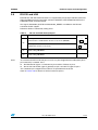
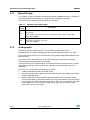
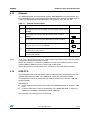
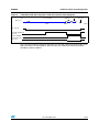
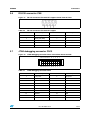
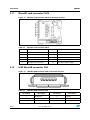
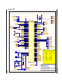
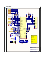
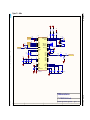
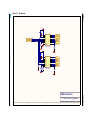
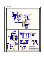
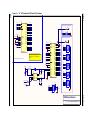
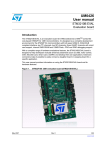
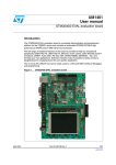
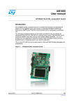
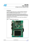
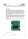
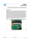
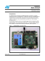
UM0600
User manual
STM3210C-EVAL
evaluation board
Introduction
The STM32F107VCT evaluation board STM3210C-EVAL is designed as a complete
development platform for STMicroelectronic's ARM Cortex-M3 core-based STM32F107VCT
microcontroller with full speed USB-OTG, ethernet MAC, two channels of CAN2.0A/B
compliant interface, 2 channels I2S, 2 channels I2C, 5 channels USART with smartcard
support, 3 channels SPI, internal 64 KB SRAM and 256 KB Flash, JTAG and SWD
debugging support.
The full range of hardware features on the board help you evaluate all peripherals (USBOTG FS, ethernet, motor control, CAN, microSD CardTM, smartcard, USART, audio DAC,
MEMS, EEPROM… etc.) and develop your own applications. Extension headers make it
easy to connect a daughterboard or wrapping board for your specific application.
Figure 1.
February 2011
STM3210C-EVAL evaluation board
Doc ID 15082 Rev 4
1/52
www.st.com
Contents
UM0600
Contents
1
2
3
2/52
Overview . . . . . . . . . . . . . . . . . . . . . . . . . . . . . . . . . . . . . . . . . . . . . . . . . . 3
1.1
Features . . . . . . . . . . . . . . . . . . . . . . . . . . . . . . . . . . . . . . . . . . . . . . . . . . . 3
1.2
Demonstration software . . . . . . . . . . . . . . . . . . . . . . . . . . . . . . . . . . . . . . . 3
1.3
Order code . . . . . . . . . . . . . . . . . . . . . . . . . . . . . . . . . . . . . . . . . . . . . . . . . 3
Hardware layout and configuration . . . . . . . . . . . . . . . . . . . . . . . . . . . . . 4
2.1
Power supply . . . . . . . . . . . . . . . . . . . . . . . . . . . . . . . . . . . . . . . . . . . . . . . 6
2.2
Boot option . . . . . . . . . . . . . . . . . . . . . . . . . . . . . . . . . . . . . . . . . . . . . . . . . 8
2.3
Clock source . . . . . . . . . . . . . . . . . . . . . . . . . . . . . . . . . . . . . . . . . . . . . . . . 8
2.4
Reset source . . . . . . . . . . . . . . . . . . . . . . . . . . . . . . . . . . . . . . . . . . . . . . . 8
2.5
Audio . . . . . . . . . . . . . . . . . . . . . . . . . . . . . . . . . . . . . . . . . . . . . . . . . . . . . 9
2.6
EEPROM . . . . . . . . . . . . . . . . . . . . . . . . . . . . . . . . . . . . . . . . . . . . . . . . . . 9
2.7
CAN . . . . . . . . . . . . . . . . . . . . . . . . . . . . . . . . . . . . . . . . . . . . . . . . . . . . . . 9
2.8
RS-232 and IrDA . . . . . . . . . . . . . . . . . . . . . . . . . . . . . . . . . . . . . . . . . . . 10
2.9
Motor control . . . . . . . . . . . . . . . . . . . . . . . . . . . . . . . . . . . . . . . . . . . . . . 11
2.10
Smartcard . . . . . . . . . . . . . . . . . . . . . . . . . . . . . . . . . . . . . . . . . . . . . . . . . 12
2.11
MicroSD card . . . . . . . . . . . . . . . . . . . . . . . . . . . . . . . . . . . . . . . . . . . . . . 13
2.12
Analog input . . . . . . . . . . . . . . . . . . . . . . . . . . . . . . . . . . . . . . . . . . . . . . . 13
2.13
Ethernet . . . . . . . . . . . . . . . . . . . . . . . . . . . . . . . . . . . . . . . . . . . . . . . . . . 14
2.14
USB-OTG . . . . . . . . . . . . . . . . . . . . . . . . . . . . . . . . . . . . . . . . . . . . . . . . . 14
2.15
MEMS . . . . . . . . . . . . . . . . . . . . . . . . . . . . . . . . . . . . . . . . . . . . . . . . . . . . 15
2.16
Development and debug support . . . . . . . . . . . . . . . . . . . . . . . . . . . . . . . 15
2.17
Display and input devices . . . . . . . . . . . . . . . . . . . . . . . . . . . . . . . . . . . . . 16
2.18
IDD measurement . . . . . . . . . . . . . . . . . . . . . . . . . . . . . . . . . . . . . . . . . . 17
Connectors . . . . . . . . . . . . . . . . . . . . . . . . . . . . . . . . . . . . . . . . . . . . . . . 19
3.1
Motor control connector CN17 . . . . . . . . . . . . . . . . . . . . . . . . . . . . . . . . . 19
3.2
Analog input connector CN10 and CN11 . . . . . . . . . . . . . . . . . . . . . . . . . 20
3.3
CAN D-type 9-pin male connector CN3 and CN4 . . . . . . . . . . . . . . . . . . 20
3.4
Ethernet RJ45 connector CN1 . . . . . . . . . . . . . . . . . . . . . . . . . . . . . . . . . 21
3.5
Trace debugging connector CN12 . . . . . . . . . . . . . . . . . . . . . . . . . . . . . . 21
Doc ID 15082 Rev 4
UM0600
4
Contents
3.6
RS-232 connector CN6 . . . . . . . . . . . . . . . . . . . . . . . . . . . . . . . . . . . . . . 22
3.7
JTAG debugging connector CN13 . . . . . . . . . . . . . . . . . . . . . . . . . . . . . . 22
3.8
Daughterboard extension connector CN8 and CN9 . . . . . . . . . . . . . . . . . 23
3.9
Audio jack CN7 . . . . . . . . . . . . . . . . . . . . . . . . . . . . . . . . . . . . . . . . . . . . . 26
3.10
TFT LCD connector CN14 . . . . . . . . . . . . . . . . . . . . . . . . . . . . . . . . . . . . 26
3.11
MicroSD card connector CN16 . . . . . . . . . . . . . . . . . . . . . . . . . . . . . . . . . 27
3.12
USB MicroAB connector CN2 . . . . . . . . . . . . . . . . . . . . . . . . . . . . . . . . . 27
3.13
Power connector CN18 . . . . . . . . . . . . . . . . . . . . . . . . . . . . . . . . . . . . . . 28
3.14
Smartcard connector CN5 . . . . . . . . . . . . . . . . . . . . . . . . . . . . . . . . . . . . 28
Schematics . . . . . . . . . . . . . . . . . . . . . . . . . . . . . . . . . . . . . . . . . . . . . . . 29
Appendix A STM3210C-EVAL I/O assignment . . . . . . . . . . . . . . . . . . . . . . . . . . . 47
Revision history . . . . . . . . . . . . . . . . . . . . . . . . . . . . . . . . . . . . . . . . . . . . . . . . . . . . 51
Doc ID 15082 Rev 4
3/52
Overview
UM0600
1
Overview
1.1
Features
1.2
●
Three 5 V power supply options: Power jack, USB connector or daughterboard.
●
Boot from user Flash, system memory or SRAM.
●
I2S audio DAC, stereo audio jack.
●
2 GByte (or more) microSD CardTM.
●
Both type A and B smartcard support.
●
I2C compatible serial interface 64 Kbit EEPROM, MEMS and I/O expander.
●
RS-232 communication.
●
IrDA transceiver.
●
USB-OTG full speed, USB microAB connector.
●
IEEE-802.3-2002 compliant ethernet connector.
●
Two channels of CAN2.0A/B compliant connection.
●
Inductor motor control connector.
●
JTAG and trace debug support.
●
3.2" 240x320 TFT color LCD with touch screen.
●
Joystick with 4-direction control and selector.
●
Reset, Wakeup, Tamper and User button.
●
4 color LEDs.
●
RTC with backup battery.
●
MCU consumption measurement circuit.
●
Extension connector for daughterboard or wrapping board.
Demonstration software
Demonstration software is preloaded in the board’s Flash memory for easy demonstration of
device peripherals in stand-alone mode. For more information and to download the latest
version available, please refer to STM3210C-EVAL demonstration firmware available on the
web: www.st.com/mcu.
1.3
Order code
To order the STM32F107VCT evaluation board, use the order code STM3210C-EVAL.
4/52
Doc ID 15082 Rev 4
UM0600
Hardware layout and configuration
2
Hardware layout and configuration
The STM3210C-EVAL evaluation board is designed around the STM32F107VCT in a 100pin LQFP package. The hardware block diagram Figure 2 illustrates the connection between
the STM32F107VCT and peripherals (LCD, EEPROM, MEMS, USART, IrDA, USB-OTG,
ethernet, audio, CAN bus, smartcard, microSD card and motor control) and Figure 3 helps
you locate these features on the actual evaluation board.
Figure 2.
Hardware block diagram
I2S2
3.3V regulator
MCU
consumption
measurement
LEDs,Key
Audio DAC
I2C1
MEMS
EEPROM
GPIO
Joystick
Extension
connector for
GPIOs
I/O expander
Touchscreen
TFT LCD
USB microAB
connector
OTG
MicroSD
Card
SPI3
MC control
connector
MC
JTAG
USB power
switch
STM32F107VCT
MII/RMII
2 BNC connector
CAN
transceiver
CAN
DB9 connector
CAN2
CAN
transceiver
CAN
DB9 connector
RS-232
transceiver
USART 2
DB9 connector
ADC
USART2
IrDA
transceiver
Potentiometer
Battery voltage
measurement
Integrated RJ45
connector
CAN1
Debug
Trace
PHY
USART3
Doc ID 15082 Rev 4
Smartcard
interface
Smartcard
connector
5/52
Hardware layout and configuration
Figure 3.
UM0600
STM3210C-EVAL evaluation board layout
CN10, CN11 BNC
CN8, CN9 Extension header
CN17 Motor control
CN1
RJ45
connector
CN4
CAN2
CN6
RS-232
U9
STM32F107VCT
CN3
CAN1
CN2
USB microAB
connector
CN12
Trace
CN18
5V power
CN13
JTAG
CN7
Audio jack
CN14
Color LCD
CN16
MicroSD card
U12
IrDA
CN5
Smartcard
RV1
Potentiometer
B1
Reset
B3
User key
B2 Wakeup
6/52
B4 Tamper
Doc ID 15082 Rev 4
U15 Joystick
UM0600
2.1
Hardware layout and configuration
Power supply
The STM3210C-EVAL evaluation board is designed to be powered by a 5 V DC power
supply and to be protected by PolyZen from a wrong power plug-in event.
It is possible to configure the evaluation board to use any of following three sources for the
power supply.
●
5 V DC power adapter connected to CN18, the power jack on the board (PSU on silk
screen for power supply unit).
●
5 V DC power with 500 mA limitation from CN2, the USB MicroAB connector (USB on
silkscreen).
●
5 V DC power from both CN8 and CN9, the extension connector for daughterboard
(DTB for daughterboard on silkscreen).
The power supply is configured by jumpers JP24 and JP25 as described in Table 1. To
enable MCU power consumption measurement, JP1, JP14 and JP23 should be reconfigured as described in Table 2.
Table 1.
Power related jumpers
Jumper
Description
PSU
DTB
USB
For power supply from the daughterboard connectors (CN8 and CN9) to
STM3210C-EVAL only, JP25 is set as shown:
PSU
DTB
USB
JP25 selects one of the three possible power supply resources.
For power supply jack (CN18) to the STM3210C-EVAL only, JP25 is set as
shown: (Default)
Configuration
JP25
Vbat is connected to 3.3 V power when JP24 is set as shown: (Default)
PSU
DTB
USB
For power supply from power supply jack (CN18) to both STM3210CEVAL and daughterboard connected on CN8 and CN9, JP25 is set as
shown to the right (the daughterboard must not have its own power supply
connected):
PSU
DTB
USB
For power supply from USB (CN2) to STM3210C-EVAL only, JP25 is set
as shown:
1 2 3
JP24
Vbat is connected to battery when JP24 is set as shown:
Warning:
1 2 3
When the board is connected to a USB host via CN2 and powered
by an external power supply (JP25 in position PSU) it is
mandatory to remove the USB cable when the external power
supply is OFF, else an unexpected current is provided by USB
VBUS which maintains a residual voltage on the board.
Doc ID 15082 Rev 4
7/52
Hardware layout and configuration
UM0600
Table 2.
MCU power consumption measurement related jumpers
Jumper
Description
PC13 is connected to anti-tamper button when JP1 is set as shown:
(Default)
JP1
PC13 is connected to MCU consumption measurement circuit as
IDD_CNT_EN signal when JP1 is set as shown. In this position PC13 is
reserved to enable or clear the counter U24 used to measure IDD when
the MCU is in low power mode.
Configuration
1 2 3
1 2 3
PA0 is connected to WUKP button and MCU power consumption
measurement circuit as LP_WAKEUP when JP14 is set as shown:
1 2 3
PA0 is connected to ethernet PHY as signal MII_CRS when JP14 is set as
shown: (Default)
1 2 3
JP14
Connect +3.3V power to MCU directly when JP23 is set as shown: The
MCU current consumption measurement can be done manually by an
ammeter connected on PJ23 pin 1 & 2. (Default)
JP23
Connect +3.3 V power to MCU with MCU current-sampling resister (1 ohm
or 1 Kohm) in series and IDD current measurement circuit in parallel when
JP23 is set as shown to the right. MCU power consumption measurement
is enabled.
1 2 3
1 2 3
The LED LD7 is lit when the STM3210C-EVAL board is powered by the 5 V correctly.
8/52
Doc ID 15082 Rev 4
UM0600
2.2
Hardware layout and configuration
Boot option
The STM3210C-EVAL board is able to boot from:
●
Embedded user Flash
●
System memory with boot loader for ISP
●
Embedded SRAM for debugging
The boot option is configured by setting switches SW1 (BOOT1) and SW2 (BOOT0).
The BOOT0 can be configured also via the RS-232 connector CN6 when JP18 is fitted.
Table 3.
Boot related switches
Switch
Boot from
Configuration
STM3210C-EVAL boots from User Flash when SW2 is set as shown to
the right. SW1 setting does not matter in this configuration. (Default)
SW1
and
SW2
SW2
0<
>1
SW1
STM3210C-EVAL boots from System Memory when SW1 and SW2 are
set as shown:
SW2
0<
>1
SW1
STM3210C-EVAL boots from Embedded SRAM when SW1 and SW2
are set as shown:
SW2
0<
2.3
>1
Clock source
Two clock sources are available on the STM3210C-EVAL evaluation board for
STM32F107VCT and RTC is embedded.
2.4
●
X2, 32 kHz crystal for embedded RTC.
●
X3, 25 MHz crystal with socket for an STM32F107VCT microcontroller, it can be
removed from the socket when an internal RC clock is used.
Reset source
The reset signal of the STM3210C-EVAL board is active low and the reset sources include:
●
Reset button, B1
●
Debugging tools from JTAG connector CN13 and trace connector CN12
●
Daughterboard from CN9
●
RS-232 connector CN6 for ISP when JP19 is fitted.
Table 4.
Jumper
JP20
Reset related jumper
Description
Enables reset of the STM32F107VCT embedded JTAG TAP controller each time a system
reset occurs. JP20 connects the TRST signal from the JTAG connection with the system
reset signal RESET#. Default setting: Not fitted.
Doc ID 15082 Rev 4
9/52
Hardware layout and configuration
2.5
UM0600
Audio
The STM3210C-EVAL evaluation board supports stereo audio play by using an audio DAC
CS43L22 connected to both an I2S2 port and one channel of the DAC of microcontroller
STM32F107VCT. The CS43L22 can be configured via the I2C1 bus when JP9 is fitted
(default setting). The automatic switch between the speaker and headphone is performed by
both CS43L22 and the audio jack with plug detection pin.
2.6
EEPROM
A 64 Kbit EEPROM connected to the I2C1 bus of STM32F107VCT.
Table 5.
EEPROM related jumper
Jumper
JP17
2.7
Description
The EEPROM is in Write protection mode when JP17 is open. Default setting: Fitted.
CAN
The STM3210C-EVAL evaluation board supports two channels of CAN2.0A/B compliant
CAN bus communication based on a 3.3 V CAN transceiver. High-speed mode, standby
mode and slope control mode are available and can be selected by setting JP7 for CAN1
and JP8 for CAN2.
Note:
JP9 should be kept open for CAN2 to avoid any impact from pull-up on I2C1 bus.
Table 6.
CAN1 related jumpers
Jumper
Description
CAN1 transceiver works in standby mode when JP7 is set as shown:
JP7
CAN1 transceiver works in high-speed mode when JP7 is set as shown:
(Default)
Configuration
1 2 3
1 2 3
CAN1 transceiver works in slope control mode when JP7 is open.
JP5
Table 7.
Jumper
CAN1 terminal resistor is enabled when JP5 is fitted.
Default setting: Not fitted
CAN2 related jumpers
Description
CAN2 transceiver works in standby mode when JP8 is set as shown:
JP8
CAN2 transceiver works in high-speed mode when JP8 is set as shown:
(Default)
CAN2 transceiver works in slope control mode when JP8 is open.
JP6
10/52
CAN2 terminal resistor is enabled when JP6 is fitted.
Default setting: Not fitted
Doc ID 15082 Rev 4
Configuration
1 2 3
1 2 3
UM0600
2.8
Hardware layout and configuration
RS-232 and IrDA
Both RS-232 and IrDA communications are supported by D-type 9-pin RS-232 connectors
CN6 and IrDA transceiver U12 which connect to USART2 of the STM32F107VCT on the
STM3210C-EVAL evaluation board.
Two signals, Bootloader_BOOT0 and Bootloader_RESET, are added on the RS-232
connector for ISP support.
RS-232 or IrDA are selected by setting JP16.
Table 8.
RS-232 and IrDA related jumpers
Jumper
Description
Configuration
USART2_RX is connected to RS-232 transceiver and RS-232
communication is enabled when JP16 is set as shown: (Default)
1 2 3
USART2_RX is connected to IrDA transceiver and IrDA communication is
enabled when JP16 is set as shown:
1 2 3
JP16
Note:
JP18
Bootloader_BOOT0 is disconnected from CN6 when JP18 is open.
Default setting: Not fitted
JP19
Bootloader_RESET is disconnected from CN6 when JP19 is open.
Default setting: Not fitted
To communicate with an RS-232 port on a PC, a 9-pin straight RS-232 cable (direct pin to
pin connection) is needed since:
●
On CN6 the RX signal is connected on pin 2 and the TX data on pin 3,
●
On the PC side the RX signal is generally on pin 3 and the TX signal on pin 2.
This standard 9-pin straight RS-232 cable is not provided with the board.
Refer to Section 3.6 for details on RS-232 connector pinout.
Doc ID 15082 Rev 4
11/52
Hardware layout and configuration
2.9
UM0600
Motor control
The STM3210C-EVAL evaluation board supports a three-phase brushless motor control via
a 34-pin connector CN17, which provides all required control and feedback signals to and
from a motor power-driving board.
Available signals on this connector include emergency stop, motor speed, 3 phase motor
current, bus voltage, heat sink temperature from the motor driving board and 6 channels of
PWM control signal going to the motor driving circuit.
JP 22 selects one of two kinds of synchronization methods for PFCs (power factor
correction).
The I/O pins used on the motor control connector CN17 are multiplexed with some
peripherals on the board; either motor control connector or multiplexed peripherals can be
enabled by setting jumpers JP10, JP21, JP22 and JP26.
Table 9.
Jumper
Motor control related jumpers
Description
Configuration
peripherals
JP22
JP22 allows a PFC synchronization signal to be redirected to the timer 4 input capture 3
pin, additionally to the timer 4 external trigger input. Default setting: Not fitted.
JP21
JP21 should be kept open when encoder signal is input from pin31 of CN17 while it should
be kept on close when analog signal is from pin31 of CN17 for special motor.
Default setting: Not fitted.
MC_EnA is enabled when JP10 is set as shown:
1 2 3
JP10
Audio
I2S_MCK is enabled when JP10 is set as shown: (Default)
JP26
12/52
Multiplexed
PE0 is connected to SD card detection when JP26 is fitted.
JP26 should be kept open when PE0 is used as
MC_PFCsync2. Default setting: Fitted
Doc ID 15082 Rev 4
1 2 3
MicroSD
card
UM0600
2.10
Hardware layout and configuration
Smartcard
STMicroelectronic’s smartcard interface chip ST8024 is used on the STM3210C-EVAL
board for asynchronous 3 V and 5 V smartcards.
It performs all supply protection and control functions based on the connections with the
STM32F107VCT listed in Table 10:
Table 10.
Connection between the ST8024 and STM32F107VCT
Signals of
ST8024
Description
Connect to
STM32F107VCT
5V/3V
Smartcard power supply selection pin
PC0
I/OUC
MCU data I/O line
PD8
XTAL1
Crystal or external clock input
PD10
OFF
Detect presence of a card, interrupt to MCU
PE7
RSTIN
Card reset input from MCU
PD9
CMDVCC
Start activation sequence input (active low)
PE14
Some jumpers must be re-configured to enable smartcard.
Note:
Two test points TP2 and TP3 are available on the board for AUX2 (auxiliary line to and from
card C8) and AUX1 (auxiliary line to and from card C4).
Table 11.
Jumper
Smartcard related jumpers
Description
Configuration
PD10 is connected to ethernet PHY as signal MII_RXD1 when JP11 is
set as shown: (Default)
1 2 3
PD10 is connected to smartcard interface chip as signal
smartcard_CLK when JP11 is set as shown:
1 2 3
PD9 is connected to ethernet PHY as signal MII_RXD0 when JP12 is
set as shown: (Default)
1 2 3
PD9 is connected to smartcard interface chip as signal smartcard_RST
when JP12 is set as shown:
1 2 3
PD8 is connected to ethernet PHY as signal MII_RX_DV/RMII_CRSDV
when JP13 is set as shown: (Default)
1 2 3
PD8 is connected to smartcard interface chip as signal smartcard_IO
when JP13 is set as shown:
1 2 3
JP11
JP12
JP13
Doc ID 15082 Rev 4
13/52
Hardware layout and configuration
2.11
UM0600
MicroSD card
The 2 GByte (or more) microSD card connected to SPI3 of STM32F107VCT is available on
the board. MicroSD card detection is managed by the standard I/O port PE0.
JP15 must remain fitted to enable microSD card chip select.
Table 12.
MicroSD card related jumper
Description
Jumper
2.12
JP15
JP15 enables microSD card chip select line. MicroSD card chip select is enabled when
JP15 is fitted.
JP15 should be kept open when PA4 is configured as a DAC output for audio DAC.
Default setting: Fitted.
JP26
PE0 is connected to SD card detection when JP26 is fitted. JP26 should be kept on open
when PE0 is used as MC_PFCsync2.
Default setting: Fitted.
Analog input
Two BNC connectors CN10 and CN11 are connected to PB0 and PA7 of the
STM32F107VCT as external analog input when a motor control connector is not used.
The 50 ohm terminal resister can be enabled by closing solder bridge SB3 and SB4 for each
BNC connector.
The test point TP7 and TP8 can be used for ADC precision measurement with BNC1
connector disconnected from PA7 by open SB5.
A low pass filter can be implemented for each BNC connector by replacing R141 and C64,
R143 and C65 with the value of resister and capacitor as requested by the end user’s
application.
There are also 3 analog signals available on the board:
14/52
1.
10 Kohm potentiometer RV1 connected to PC4.
2.
IDD measurement output signal connected to PA6 for power consumption test in RUN,
SLEEP and STOP mode.
3.
Battery voltage measurement output signal connected to PC5. For battery voltage
measurement VBAT is connected to ADC input using resistor divider since this voltage
may be higher than MCU_VDD when the battery is new. The resistor divider 2/3 needs
to be pulled low by an I/O expander (VBAT_DIV on EXP_IO12) in order to avoid
permanent current on this bridge.
Doc ID 15082 Rev 4
UM0600
2.13
Hardware layout and configuration
Ethernet
The STM3210C-EVAL evaluation board supports 10M/100M ethernet communication by a
PHY DP83848CVV (U1) and integrated RJ45 connector (CN1). Both MII and RMII interface
modes are supported and can be selected by setting jumpers JP2, JP3 and JP4.
Table 13.
Ethernet related jumpers
Jumper
JP2
Description
Configuration
JP2 selects MII or RMII interface mode. MII is enabled when JP2 is open
while RMII interface mode is enabled when JP2 is fitted. Default setting:
Not fitted.
JP3 should be set as shown when MII interface mode is enabled.
(Default)
1 2 3
JP3
JP3 should be set as shown when RMII interface mode is enabled.
JP4
1 2 3
25 MHz clock for MII or 50 MHz clock for RMII is provided by MCO at
PA8 when JP4 is set as shown: (Default)
1 2 3
25 MHz clock is provided by external crystal X1 (for MII interface mode
only) when JP4 is set as shown:
1 2 3
JP4 has to be kept open when the clock is provided by external oscillator
U2 (not fitted by default).
Note:
JP11, JP12, JP13 and JP14 are set to support ethernet by default, please verify the jumper
configuration before ethernet demonstration.
Note2: Test point TP1 is connected to 25MHz clock output pin of Ethernet PHY U1 which
provide 25MHz or 50MHz clock for system in MII or RMII mode.
Note3: Test point TP4 can be used for PTP_PPS feature only when R45 is removed.
2.14
USB-OTG
The STM3210C-EVAL evaluation board supports USB-OTG full speed communication via a
USB MicroAB connector (CN2) and a USB power switch (U3) connected to VBUS.
The evaluation board can be powered by this USB connection at 5 V DC with a 500 mA
current limitation.
LED LD6 is lit:
●
in Host mode when the power switch (U3) is ON (STM3210C-EVAL is acting as a USB
host),
●
in Device mode when a cable is connected to a PC (STM3210C-EVAL is acting as a
USB device and VBUS is powered by another USB host).
LD5 is lit when over-current occurs in Host mode.
Doc ID 15082 Rev 4
15/52
Hardware layout and configuration
2.15
UM0600
MEMS
An ST MEMS device LIS302DL is connected to the I2C1 bus of STM32F107VCT.
2.16
Development and debug support
The two debug connectors available on STM3210C-EVAL evaluation board are:
16/52
1.
CN13, standard 20-pin JTAG interface connector that is compliant with the debug tools
of ARM7 and ARM9 and cortex M3.
2.
CN12, SAMTEC 20-pin connector FTSH-110-01-L-DV for both SWD and trace that is
compliant with ARM CoreSightTM debug tools.
Doc ID 15082 Rev 4
UM0600
2.17
Hardware layout and configuration
Display and input devices
The 3.2” TFT color LCD connected to SPI3 and 4 general purpose color LED’s (LD 1,2,3,4)
are available as display devices.
A touch screen connected to an I/O expander (U7), 4-direction joystick with selection key,
general purpose button (B3), wakeup button (B2) and tamper detection button (B4) are
available as input devices.
JP14 should be re-configured to enable wakeup button B2 which shares the same I/O as
MII_CRS of the ethernet. You may refer to Table 2 for details.
The STM3210C-EVAL board also supports a second optional 2.4” TFT LCD without touch
screen that can be mounted on CN15 connector. The 2.4” TFT LCD is not populated by
default.
Table 14 shows both the LCD modules pin connections.
Table 14.
LCD modules
3.2" TFT LCD with touch screen
CN14 (default)
Pin on CN14
Description
Pin connection
2.4" TFT LCD CN15
(optional)
Pin on CN15
Description
Pin connection
1
CS
PB2
1
CS
PB2
2
RS
-
2
SCL
PC10
3
WR/SCL
PC10
3
SDI
PC12
4
RD
-
4
RS
-
5
RESET
RESET#
5
WR
-
22
BL_GND
GND
6
RD
-
23
BL_control
+5V
7
SDO
PC11
24
VDD
3.3V
8
RESET
RESET#
25
VCI
3.3V
9
VDD
3.3V
26
GND
GND
10
VCI
3.3V
27
GND
GND
11
GND
GND
28
BL_VDD
+5V
12
GND
GND
29
SDO
PC11
13
BL_VDD
3.3V
30
SDI
PC12
14
BL_Control
3.3V
31
XL
IO Expander
15
BL_GND
GND
32
XR
IO Expander
16
BL_GND
GND
33
YD
IO Expander
34
YU
IO Expander
Doc ID 15082 Rev 4
17/52
Hardware layout and configuration
2.18
UM0600
IDD measurement
Figure 4.
STM3210C-EVAL IDD measurement circuit
The circuit above is implemented on STM3210C-EVAL for IDD measurement.
In Run mode, IDD current is measured using MAX9938FEUK+ (U21) connected to the
1ohm shunt resistor. In this case IDD_CNT_EN remains high during measurement and
JP23 jumper must be set to 2<->3.
In Stop or Standby mode, the operational amplifier MAX9938FEUK+ (U21) is connected on
the 1 Kohm shunt resistor.
To measure a current corresponding to the Stop or Standby modes the procedure is:
1.
Configure ADC to measure voltage on IDD_measurement pin.
2.
Configure PA0 as interrupt input on falling edge.
3.
Enter in Stop or Standby modes with IDD_CNT_EN Low.
4.
LP_WAKEUP falling edge wakeup the MCU after 100 ms.
5.
Start ADC conversion as soon as possible after wakeup in order to measure the
voltage corresponding to Low power mode on 1 uF capacitor.
6.
Reset the counter by programming IDD_CNT_EN High in less than 50 mS after the
wakeup to avoid 1 Kohm to be connected later on VDD_MCU.
In Stop or Standby modes, the 1K resistor is connected when T2 goes off after entering the
Stop or Standby mode. Q13 output of the counter allows connection of the 1K resistor when
the current IDD becomes very low. Figure 5 shows the measurement timing.
18/52
Doc ID 15082 Rev 4
UM0600
Figure 5.
Hardware layout and configuration
STM3210C-EVAL IDD Low power mode measurement timing diagram
IDD measure
Run
Stop or Standby
Wake-up
Clear CNT
MCU mode
0
150ms
300ms
450ms
IDD_CNT_EN
Q13=LOW_POWER_EN
(T2 pin 3)
Q14=LP_WAKEUP
Q14n=Switch control
(U22 pin 4)
The Low power mode measurement procedure can be used in Stop or Standby modes if the
IDD current does not exceed 60 uA, otherwise the Run mode measurement procedure
should be used up to 60 mA.
Doc ID 15082 Rev 4
19/52
Connectors
UM0600
3
Connectors
3.1
Motor control connector CN17
Figure 6.
Motor control connector CN17 viewed from above the PCB
Table 15.
Motor control connector CN17
Description
20/52
Pin of
Pin number
STM32F107VCT
of CN17
Pin number
Pin of
Description
of CN17
STM32F107VCT
Emergency stop
PE15
1
2
GND
PWM-UH
PE9
3
4
GND
PWM-UL
PE8
5
6
GND
PWM-VH
PE11
7
8
GND
PWM-VL
PE10
9
10
GND
PWM-WH
PE13
11
12
GND
PWM-WL
PE12
13
14
PHASE A current
PA7
15
16
GND
PHASE B current
PB0
17
18
GND
PHASE C current
PB1
19
20
GND
NTC bypass relay
PD2
21
22
GND
Dissipative brake
PWM
PA0
23
24
GND
+5V power
+5V
25
26
PFC SYNC
PE0 and PD14
27
28
VDD_Micro
PFC PWM
PD15
29
30
GND
Encoder A
PC6 via JP10
31
32
GND
Encoder B
PC7
33
34
Doc ID 15082 Rev 4
PA5
PC0
PC8
Bus voltage
Heat sink
temperature
Encoder
index
UM0600
3.2
Connectors
Analog input connector CN10 and CN11
Figure 7.
Analog input connector CN10 and CN11 viewed from the bottom
Table 16.
Analog input connector CN10 and CN11
Pin number
3.3
Description
Pin number
Description
1
GND
4
GND
2
GND
5
Analog input PB0 and PA7 for
CN10 and CN11 respectively
3
GND
CAN D-type 9-pin male connector CN3 and CN4
Figure 8.
CAN D-type 9-pin male connector CN3 and CN4 viewed from the front
Table 17.
CAN D-type 9-pin male connector CN3 and CN4
Pin number
1,4,8,9
2
Description
NC
Pin number
7
CANL
3,5,6
Doc ID 15082 Rev 4
Description
CANH
GND
21/52
Connectors
3.4
UM0600
Ethernet RJ45 connector CN1
Figure 9.
Ethernet RJ45 connector CN1 viewed from the front
Table 18.
RJ45 connector CN1
Pin number
3.5
Description
Pin number
Description
1
TxData+
2
TxData-
3
RxData+
4
Shield
5
Shield
6
RxData-
7
Shield
8
Shield
Trace debugging connector CN12
Figure 10. Trace debugging connector CN12 viewed from above the PCB
Table 19.
1
20 18 16 14 12 10 8 6 4
2
Trace debugging connector CN12
Pin number
22/52
19 17 15 13 11 9 7 5 3
Description
Pin number
Description
1
3.3V power
2
TMS/PA13
3
GND
4
TCK/PA14
5
GND
6
TDO/PB3
7
KEY
8
TDI/PA15
9
GND
10
RESET#
11
GND
12
TraceCLK/PE2
13
GND
14
TraceD0/PE3 or SWO/PB3
15
GND
16
TraceD1/PE4 or nTRST/PB4
17
GND
18
TraceD2/PE5
19
GND
20
TraceD3/PE6
Doc ID 15082 Rev 4
UM0600
3.6
Connectors
RS-232 connector CN6
Figure 11. RS-232 connector CN6 with ISP support viewed from the front
Table 20.
RS-232 connector CN6 with ISP support
Pin number
3.7
Description
Pin number
Description
1
Bootloader_RESET
6
NC
2
RS232_RX (PD6)
7
NC
3
RS232_TX (PD5)
8
Bootloader_BOOT0
4
NC
9
NC
5
GND
JTAG debugging connector CN13
Figure 12. JTAG debugging connector CN13 viewed from above the PCB
Table 21.
19 17 15 13 11 9 7 5 3
1
20 18 16 14 12 10 8 6 4
2
JTAG debugging connector CN13
Pin number
Description
Pin number
Description
1
3.3V power
2
3.3V power
3
PB4
4
GND
5
PA15
6
GND
7
PA13
8
GND
9
PA14
10
GND
11
RTCK
12
GND
13
PB3
14
GND
15
RESET#
16
GND
17
DBGRQ
18
GND
19
DBGACK
20
GND
Doc ID 15082 Rev 4
23/52
Connectors
3.8
UM0600
Daughterboard extension connector CN8 and CN9
Two 50-pin male headers CN8 and CN9 can be used to connect a daughterboard or
standard wrapping board to the STM3210C-EVAL evaluation board. All 80 GPI/Os are
available on it.
The space between these two connectors and power position, GND and RESET pin are
defined as a standard, which allows to develop common daughterboards for several
evaluation boards.
The standard width between CN8 pin1 and CN9 pin1 is 2700 mils (68.58mm). This standard
is implemented on the majority of evaluation boards.
Each pin on CN8 and CN9 can be used by a daughterboard after disconnecting it from the
corresponding function block on the STM3210C-EVAL evaluation board. Please refer to
Table 22 and Table 23 for details.
Table 22.
Pin
Daughterboard extension connector CN8
Description
Alternative function
How to disconnect with function block on STM3210C-EVAL
1
GND
-
3
PC7
MC
Disconnect STM3210C-EVAL board from motor power drive board
5
PC9
USB power switch On
Remove R36
7
PA9
USB VBUS
Remove R78
9
PA0
MC/Ethernet/WKUP
Keep JP14 open. Disconnect STM3210C-EVAL board from motor
power drive board.
11
PC14 via SB1 32kHz oscillator
Remove R161, close SB1
13
PA12
Remove R43 or disconnect USB cable
15
PC15 via SB2 32kHz oscillator
17
PC10
SPI1_CLK
19
GND
-
21
PC12
SPI1_MOSI
23
PD1
CAN1_TX
25
PD3
LD3
27
PD5
USART2_TX
29
PD7
LD1
33
PB3
TDO/SWO
35
PB5
CAN2_RX
Remove R45
37
PB7
I2C1_SDA
Remove R132
39
GND
-
41
PE2
Trace_CK
43
PE4
Trace_D1
45
PB8
MC
USB_DP
Remove R59, close SB2
Remove R96
Remove R94
31
24/52
Disconnect STM3210C-EVAL board from motor power drive board
Doc ID 15082 Rev 4
UM0600
Table 22.
Pin
Connectors
Daughterboard extension connector CN8 (continued)
Description
Alternative function
How to disconnect with function block on STM3210C-EVAL
47
PE6
Trace_D3
49
D5V
2
PC6
I2S_MCK/MC
JP10 open
4
PC8
MC
Disconnect STM3210C-EVAL board from motor power drive board
6
PA8
MCO
JP4 open
8
PA10
USB_ID
Remove R38 or disconnect USB cable
10
GND
12
PA11
USB_DM
Remove R42 or disconnect USB cable
14
PA13
TMS/SWDIO
16
PA14
TCK/SWCLK
18
PC11
SPI1_MISO
20
PA15
TDI
22
PD0
CAN1_RX
Remove R44
24
PD2
MC
Disconnect STM3210C-EVAL board from motor power drive board.
26
PD4
LD4
Remove R97
28
PD6
USART2_RX
Keep JP16 open
30
GND
Remove R135 and LCD
32
34
PB4
TRST
Keep JP20 open
36
PB6
CAN2_TX/ I2C1_SCK
Keep JP9 open
38
PE0
MC/MicroSD card
detection
Remove MicroSD card. Disconnect STM3210C-EVAL board from
motor power drive board.
40
PE1
USB_Ove-current
Remove R35
42
PE3
Trace_D0
44
PE5
Trace_D2
46
PB9
User Button
48
3V3
50
GND
Remove R104
Doc ID 15082 Rev 4
25/52
Connectors
Table 23.
Pin
UM0600
daughterboard extension connector CN9
Description
Alternative function
How to disconnect with component on STM3210C-EVAL board
1
GND
-
3
PD14
MC
Keep JP22 open. Disconnect STM3210C-EVAL board from motor
power drive board.
5
PD12
Ethernet
Remove RS2
7
PD10
Ethernet/Smartcard
Keep JP11 open
9
PC13 button
B3
IDD_CNT_EN /
Anti-tamper button B4
Keep JP1 open
11
RESET#
-
13
PB15
I2S_DIN
15
PB13
I2S_CK / Ethernet
Remove RS3
17
PB11
Ethernet
Remove RS3
19
D5V
-
21
PE14
Smartcard_CMDVCC
25
PE12
MC
27
PE10
MC
29
PE8
MC
31
PE7
Smartcard_OFF
Remove R69
33
PB1
MC
Remove R168
35
PC5
VBAT_voltage
Remove R154
37
PA7
MC
Remove R169
39
GND
41
PA4
MicroSD card /
Audio_DAC
Keep JP15 open
43
PA2
Ethernet
Remove R162
45
PC3
Ethernet
Remove RS1
47
PC1
Ethernet
49
PC13
IDD_CNT_EN /
Anti-tamper button B4
Keep JP1 open
2
PD15
MC
Disconnect STM3210C-EVAL board from motor power drive board
4
PD13
LD2
Remove R95
6
PD11
Ethernet
Remove RS1
8
PD9
Ethernet / Smartcard
Keep JP12 open
10
GND
12
PD8
Ethernet / Smartcard
Keep JP13 open
14
PB14
IO_Expandor_INT
Remove R159
Remove R166
23
26/52
Disconnect STM3210C-EVAL board from motor power drive board
Doc ID 15082 Rev 4
UM0600
Table 23.
Connectors
daughterboard extension connector CN9 (continued)
Pin
Description
Alternative function
How to disconnect with component on STM3210C-EVAL board
16
PB12
Ethernet / Audio
Remove RS3
18
PB10
Ethernet
Remove RS2
20
PE15
MC
Remove R139
22
PE13
MC
Disconnect STM3210C-EVAL board from motor power drive board
26
PE11
MC
28
PE9
MC
30
GND
32
PB2
MC
Remove R168
34
PB0
MC
Remove R167
36
PC4
Potentiometer
Remove R103
38
PA6
IDD_Measurement
Remove R79
40
PA5
MC
Remove R84
42
PA3
MC / Ethernet
Keep JP10 open
44
PA1
Ethernet
Keep JP3 open
46
PC2
Ethernet
Remove RS1
48
PC0
MC / Smartcard
Remove R165
50
GND
24
Disconnect STM3210C-EVAL board from motor power drive board
3.9
Audio jack CN7
A 3.5 mm stereo audio jack CN7 connected to audio DAC is available on the
STM3210C-EVAL board.
3.10
TFT LCD connector CN14
One 34-pin male header CN14 is available on the board to connect LCD module board
MB785. Please refer to Chapter 2.17 for detail.
Doc ID 15082 Rev 4
27/52
Connectors
3.11
UM0600
MicroSD card connector CN16
Figure 13. MicroSD card connector CN16 viewed from the front
Table 24.
MicroSD card connector CN16
Pin number
Description
Pin number
1
3.12
Description
6
Vss/GND
MicroSDcard_DOUT(PC11)
2
MicroSDcard_CS (PA4)
7
3
MicroSDcard_DIN(PC12)
8
4
+3V3
9
GND
5
MicroSDcard_CLK (PC10)
10
MicroSDcard_detect (PE0)
USB MicroAB connector CN2
Figure 14. USB MicroAB connector CN2 viewed from the front
Table 25.
USB MicroAB connector CN2
Pin number
28/52
Description
Pin number
Description
1
VBUS (PA9)
4
ID (PA10)
2
D- (PA11)
5
GND
3
D+ (PA12)
Doc ID 15082 Rev 4
UM0600
3.13
Connectors
Power connector CN18
Your STM3210C-EVAL evaluation board can be powered from a DC 5 V power supply via
the external power supply jack (CN18) shown in Figure 15. The central pin of CN18 must be
positive.
Figure 15. Power supply connector CN18 viewed from the front
DC +5V
GND
3.14
Smartcard connector CN5
Figure 16. Smartcard connector CN5
1234
17 18
5678
Table 26.
Smartcard connector CN5
Pin number
Description
Pin number
Description
1
VCC
5
GND
2
RST
6
NC
3
CLK
7
I/O
4
NC
8
NC
17
Detection pin of card presence
18
Detection pin of card presence
Doc ID 15082 Rev 4
29/52
Schematics
4
UM0600
Schematics
This section provides the following schematics:
30/52
●
Figure 17: STM3210C on page 31
●
Figure 18: MCU on page 32
●
Figure 19: Ethernet on page 33
●
Figure 20: Full speed USB-OTG on page 34
●
Figure 21: Audio on page 35
●
Figure 22: LCD on page 36
●
Figure 23: I/O expander on page 37
●
Figure 24: CAN on page 38
●
Figure 25: RS-232 and IrDA on page 39
●
Figure 26: Smartcard on page 40
●
Figure 27: Motor control on page 41
●
Figure 28: I/O peripherals on page 42
●
Figure 29: Extension connector on page 43
●
Figure 30: JTAG and trace on page 44
●
Figure 31: MicroSD card on page 45
●
Figure 32: Power on page 46
●
Figure 33: 3.2” LCD module with SPI and 16-bit interface on page 47
Doc ID 15082 Rev 4
UM0600
Figure 17. STM3210C
U_Audio
Audio.SchDoc
U_MCU
MCU.SchDoc
Audio_RST
Audio_DAC_OUT
Audio_SDA
Audio_SCK
I2S_CK
I2S_DIN
I2S_CMD
I2S_MCK
Audio_DAC_OUT
I2S_CK
I2S_DIN
I2S_CMD
I2S_MCK
U_CAN
CAN.SchDoc
CAN1_RX
CAN1_TX
CAN2_RX
CAN2_TX
CAN1_RX
CAN1_TX
CAN2_RX
CAN2_TX
U_MicroSDCard
MicroSDCard.SchDoc
MicroSDCard_MISO
MicroSDCard_Detection
MicroSDCard_CS
MicroSDCard_MOSI
MicroSDCard_SCK
MicroSDCard_Detection
MicroSDCard_CS
U_MotorControl
MotorControl.SchDoc
MC_PFCsync1
MC_PFCsync2
MC_WL
MC_VH
MC_VL
MC_UH
MC_UL
MC_WH
MC_NTC
MC_DissipativeBrake
MC_PFCpwm
MC_EnIndex
MC_BusVoltage
MC_HeatsinkTemperature
MC_EnB
MC_EnA
MC_CurrentC
MC_CurrentB
MC_CurrentA
MC_EmergencySTOP
U_JTAG&Trace
JTAG&Trace.SchDoc
Doc ID 15082 Rev 4
TDI
RESET#
TRST
TMS/SWDIO
TCK/SWCLK
TDO/SWO
TRACE_CK
TRACE_D0
TRACE_D1
TRACE_D2
TRACE_D3
TDI
RESET#
TRST
TMS/SWDIO
TCK/SWCLK
TDO/SWO
TRACE_CK
TRACE_D0
TRACE_D1
TRACE_D2
TRACE_D3
U_Ethernet
Ethernet.SchDoc
MII_TX_CLK
MII_TXD0
MII_TXD1
MII_TXD2
MII_TXD3
MII_INT
MII_TX_EN
MII_RX_ER
MII_RX_DV/RMII_CRSDV
MII_RX_CLK/RMII_REF_CLK
MII_RXD0
MII_RXD1
MII_RXD2
MII_RXD3
MII_COL
MII_CRS
MII_MDIO
MII_MDC
MCO
PHY_RESET#
MII_TX_CLK
MII_TXD0
MII_TXD1
MII_TXD2
MII_TXD3
MII_TX_EN
MII_RX_ER
MII_RX_DV/RMII_CRSDV
MII_RX_CLK/RMII_REF_CLK
MII_RXD0
MII_RXD1
MII_RXD2
MII_RXD3
MII_COL
MII_CRS
MII_MDIO
MII_MDC
MCO
SmartCard_CMDVCC
SmartCard_CLK
SmartCard_RST
SmartCard_IO
SmartCard_3/5V
SmartCard_OFF
SmartCard_CMDVCC
SmartCard_CLK
SmartCard_RST
SmartCard_IO
SmartCard_3/5V
SmartCard_OFF
U_Power
Power.SchDoc
IDD_Measurement
VBAT_Voltage
LP_WAKEUP
VBAT_DIV
IDD_CNT_EN
IDD_CNT_EN
U_USART&IrDA
USART&IrDA.SchDoc
BNC1
BNC2
JOY_SEL
JOY_DOWN
JOY_LEFT
JOY_RIGHT
JOY_UP
MEMS_INT1
MEMS_INT2
U_IO_Expandor
IO_Expandor.SchDoc
I2C1_SCK
I2C1_SDA
IO_Expandor_INT
R131
R132
0
0
IO_Expandor_SCK
IO_Expandor_SDA
IO_Expandor_INT
EXP_IO12
EXP_IO11
EXP_IO10
EXP_IO9
EXP_IO8
EXP_IO7
EXP_IO6
EXP_IO5
EXP_IO4
EXP_IO3
EXP_IO2
EXP_IO1
TouchScreen_YTouchScreen_Y+
TouchScreen_XTouchScreen_X+
R133 R134
4K7 4K7
+3V3
U_LCD
LCD.SchDoc
LCD_CS
SPI3_SCK
SPI3_MOSI
LCD_CS
LCD_CLK
LCD_DI
RESET#
LCD_DO
TouchScreen_YTouchScreen_Y+
TouchScreen_XTouchScreen_X+
U_ExtensionConnector
ExtensionConnector.SchDoc
PA[0..15]
PB[0..15]
PC[0..15]
PD[0..15]
PE[0..15]
PA[0..15]
PB[0..15]
PC[0..15]
PD[0..15]
PE[0..15]
RESET#
U_USB_OTG_FS
USB_OTG_FS.SchDoc
USB_PowerSwitchOn
USB_DM
USB_DP
USB_ID
USB_VBUS
USB_OverCurrent
USB_PowerSwitchOn
USB_DM
USB_DP
USB_ID
USB_VBUS
USB_OverCurrent
Note1: only decoupling capacitors value was updated from Versioin B.1 to B.2.
Note2: only assembly request of R42 and R43 was updated from Versioin B.2 to B.3.
31/52
STMicroelectronics
Title:
STM3210C-EVAL
Number:MB784
Rev: B.3(PCB.SCH) Date: 9/18/2009
Sheet 1
of
16
Schematics
USART2_RX
USART2_TX
Bootloader_RESET
Bootloader_BOOT0
LED4
LED3
LED2
LED1
EEPROM_SCK
EEPROM_SDA
MEMS_SCK
MEMS_SDA
Potentiometer
Anti_Tamper
WAKEUP
User_Button
Potentiometer
Anti_Tamper
WAKEUP
User_Button
IDD_Measurement
VBAT_Voltage_OUT
USB_VBUS
RS232/IrDA_RX
RS232/IrDA_TX
Bootloader_RESET
Bootloader_BOOT0
U_IO Peripherals
IO Peripherals.SchDoc
LED4
LED3
LED2
LED1
SPI3_MISO
U_SmartCard
SmartCard.SchDoc
MC_PFCsync1
MC_PFCsync2
BNC2
MC_WL
BNC1
MC_VH
MC_VL
MC_UH
MC_UL
MC_WH
MC_NTC
MC_DissipativeBrake
MC_PFCpwm
MC_EnIndex
MC_BusVoltage
MC_HeatsinkTemperature
MC_EnB
MC_EnA
MC_CurrentC
MC_CurrentB
MC_CurrentA
MC_EmergencySTOP
1
2
TP6
MCO
MC_DissipativeBrake
C17
10pF
2
1
MII_CRS
3
2
4
1
R59
0
U9A
JP14
MII_RX_CLK/RMII_REF_CLK
MII_MDIO
MII_COL
JP15
MicroSDCard_CS
Audio_DAC_OUT
R78
USB_VBUS
0
+3V3
1 SW1
2
R60
09.03290.01
10K
MC_BusVoltage
IDD_Measurement
MC_CurrentA
MCO
USB_ID
USB_DM
USB_DP
TMS/SWDIO
TCK/SWCLK
TDI
Doc ID 15082 Rev 4
MC_CurrentB
MC_CurrentC
LCD_CS
TDO/SWO
TRST
CAN2_RX
CAN2_TX
JP9
I2C1_SDA
MII_TXD3
User_Button
MII_RX_ER
MII_TX_EN
I2C1_SCK
MII_TXD0
I2S_CMD
I2S_CK
MII_TXD1
IO_Expandor_INT
I2S_DIN
PA0
PA1
PA2
PA3
PA4
PA5
PA6
PA7
PA8
PA9
PA10
PA11
PA12
PA13
PA14
PA15
23
24
25
26
29
30
31
32
67
68
69
70
71
72
76
77
PB0
PB1
PB2
PB3
PB4
PB5
PB6
PB7
PB8
PB9
PB10
PB11
PB12
PB13
PB14
PB15
35
36
37
89
90
91
92
93
95
96
47
48
51
52
53
54
12
13
14
73
94
C18
20pF
C19
R63
R61
10K
220
PC15-OSC32_OUT
PC14-OSC32_IN
PC13-ANTI_TAMP
PC12
PC11
PC10
PC9
PC8
PC7
PC6
PC5
PC4
PC3
PC2
PC1
PC0
PB0
PB1
PB2
PB3
PB4
PB5
PB6
PB7
PB8
PB9
PB10
PB11
PB12
PB13
PB14
PB15
PD15
PD14
PD13
PD12
PD11
PD10
PD9
PD8
PD7
PD6
PD5
PD4
PD3
PD2
PD1
PD0
PE15
PE14
PE13
PE12
PE11
PE10
PE9
PE8
PE7
PE6
PE5
PE4
PE3
PE2
PE1
PE0
OSC_IN
OSC_OUT
NRST
NC
BOOT0
D1
1N4148
2
20pF
PA0-WKUP
PA1
PA2
PA3
PA4
PA5
PA6
PA7
PA8
PA9
PA10
PA11
PA12
PA13
PA14
PA15
TP4
PTP_PPS
X3
25MHz (with socket)
B1
3
SW2
09.03290.01
JP18
PA[0..15]
C16
10pF
PC15
PC14
PC13
PC12
PC11
PC10
PC9
PC8
PC7
PC6
PC5
PC4
PC3
PC2
PC1
PC0
62
61
60
59
58
57
56
55
88
87
86
85
84
83
82
81
PD15
PD14
PD13
PD12
PD11
PD10
PD9
PD8
PD7
PD6
PD5
PD4
PD3
PD2
PD1
PD0
46
45
44
43
42
41
40
39
38
5
4
3
2
1
98
97
PE15
PE14
PE13
PE12
PE11
PE10
PE9
PE8
PE7
PE6
PE5
PE4
PE3
PE2
PE1
PE0
C15
100nF
R62
+3V3
X2
MC306-G-06Q-32.768 (manufacturer JFVNY)
PC[0..15]
PD[0..15]
1
IDD_CNT_EN
2
3
SPI3_MOSI
SPI3_MISO
SPI3_SCK
USB_PowerSwitchOn
MC_EnIndex
MC_EnB
VBAT_Voltage_OUT
Potentiometer
MII_TX_CLK
MII_TXD2
MII_MDC
PE[0..15]
PA[0..15]
PB[0..15]
PC[0..15]
PD[0..15]
PE[0..15]
Anti_Tamper
JP1
1
I2S_MCK
2
3
MC_EnA
JP10
SmartCard_3/5V
R165
MC_HeatsinkTemperature
0
MC_PFCpwm
MC_PFCsync1
LED2
MII_RXD3
MII_RXD2
1
SmartCard_CLK
2
3
MII_RXD1
JP11
1
LED1
USART2_RX
USART2_TX
LED4
LED3
MC_NTC
CAN1_TX
CAN1_RX
2
3
SmartCard_RST
MII_RXD0
JP12
1
2
3
SmartCard_IO
MII_RX_DV/RMII_CRSDV
JP13
MC_EmergencySTOP
SmartCard_CMDVCC
MC_WH
MC_WL
MC_VH
MC_VL
MC_UH
MC_UL
SmartCard_OFF
TRACE_D3
TRACE_D2
TRACE_D1
TRACE_D0
TRACE_CK
USB_OverCurrent
MC_PFCsync2
Jumper configuration:
default set/ feature enabled
another set/ feature enabled
==================================================
JP1:
2<->3 / Anti_Temper
1<->2 / MCU current measurement
JP9:
close / I2C device
open / CAN2
JP10:
1<->2 / I2S Audio
2<->3 / MC
JP11:
2<->3 / Ethernet
1<->2 / Smartcard
JP12:
2<->3 / Ethernet
1<->2 / Smartcard
JP13:
2<->3 / Ethernet
1<->2 / Smartcard
JP14:
1<->2 / Ethernet
2<->3 / WKUP & MC
JP15:
close / SDcard CS
open / output for audio DAC
JP18:
open/ BL_Boot0 disabled close / BL_Boot0
JP19:
open/ BL_Reset disabled
close / BL_Reset
JP26
+3V3
MicroSDCard_Detection
STMicroelectronics
[N/A]
Bootloader_BOOT0
Title:
JP19
RESET#
Bootloader_RESET
STM3210C-EVAL MCU
Number:MB784
1N4148
2
3
Rev: B.3(PCB.SCH)
Date: 10/10/2009
4
Sheet 2
of
16
UM0600
D2
R161
0
PB[0..15]
STM32F107VCT
3
2
4
1
1
9
8
7
80
79
78
66
65
64
63
34
33
18
17
16
15
RESET
1
4
3
WAKEUP
3
3
Schematics
32/52
Figure 18. MCU
UM0600
Figure 19. Ethernet
PA0
PB10
PA3
PD12
PD11
PB8
PC2
PC3
MII_CRS
MII_RX_ER
MII_COL
MII_RXD3
MII_RXD2
MII_TXD3
MII_TXD2
MII_TX_CLK
+3V3
+3V3
R8
1K5
RS1
33
Unused in RMII mode
C1
100nF
RS2
33
1
2
3
4
5
6
33
RS4
PD10
PD9
PD8
MII_RXD1
MII_RXD0
MII_RX_DV/RMII_CRSDV
+3V3
R2
JP2
43
44
45
46
41
39
38
33
Doc ID 15082 Rev 4
2K2
42
40
PC1
PA2
MII_MDC
MII_MDIO
PHY_RESET#
R162
3
PA1
MII_RX_CLK/RMII_REF_CLK
0
MII_INT
1
R1
CN1
JP3
33
34
25
TP1
25MHz
JP4
1
2
PA8
TX_CLK
TX_EN
TXD_0
TXD_1
TXD_2
TXD_3/SNI_MODE
TD+
TDRD+
RDNC
NC
NC
NC
NC
RXD_0/PHYAD1
RXD_1/PHYAD2
RXD_2/PHYAD3
RXD_3/PHYAD4
RX_ER/MDIX_EN
RX_DV/MII_MODE
RX_CLK
3
R31
4.87K
24
37
18
23
17
16
14
13
12
11
10
9
8
1
4
2
3
5
6
9
10
12
11
COL/PHYAD0
CRS/CRS_DV/LED_CFG
MDC
MDIO
RS6
LED_LINK/AN0
LED_SPEED/AN1
LED_ACT/COL/AN_EN
RESET_N
PWR_DOWN/INT
NC
NC
To IO expandor
X1
25MHz (with socket)
MCO
29
7
2K2
R41
0
0
C10
22pF
AVDD33
IOVDD33
IOVDD33
X2
X1
25MHz_OUT
AGND
AGND
IOGND
IOGND
DGND
RBIAS
PFBIN2
PFBIN1
PFBOUT
7
8
13
14
+3V3
RD+
RCT
RDLED(green)_A
LED(green)_K
LED(Yellow)_A
LED(Yellow)_K
NC
CHS GND
Shield
Shield
J0011D21B
Second source: SI-60116-F
28
27
26
21 R6
20 R7
22
48
32
TD+
TCT
TD-
2K2
2K2
2K2
+3V3
+3V3
19
15
47
35
36
MII
RMII
====================
JP2 open
close
JP3 2<->3
1<->2
JP4 2<->3
2<->3
DP83848CVV
+3V3
U2
+3V3
4
1
R32
10K
31
30
+3V3
2
R30
C9
22pF
R13 R14
240 240
U1
RS3
PB11
PB12
PB13
MII_TX_EN
MII_TXD0
MII_TXD1
C2
100nF
RS5
50
VCC OUT
EN
GND
3
2
C3
100nF
C4
100nF
C5
100nF
C11
10uF
C6
100nF
C7
100nF
External 25MHz crystal mode
=====================
JP4 1<->2 (MCO pin free for another
application)
C8
100nF
SM7745HEV-50.0M (do not fit)
Title:
33/52
STM3210C-EVAL Ethernet
Number:MB784
Rev: B.3(PCB.SCH)
Date: 9/18/2009
Sheet 3
Schematics
STMicroelectronics
1
2
3
Schematics
34/52
Figure 20. Full speed USB-OTG
4
A
A
+3V3
R33
680
R36
0
2
5
4
+5V
B
GND FAULT
IN
OUT
EN
STMPS2141STR
3
1
LD5
Red
R35
0
PE1
CN2
1
2
3
4
5
C12
4.7uF
VBUS
DM
DP
ID
GND
Shield
B
475900001
PA9
PA11
PA12
PA10
+3V3
R42
R43
R38
22
22
0
R39
330
1
USB_VBUS
USB_DM
USB_DP
USB_ID
C
ID
D+in
D-in
Pd1
Pd2
GND
A3
C1
D1
B1
C2
C
LD6
Green
3
Vbus
D+out
D-out
Dz
Pup
2
U4
B3
C3
D3
A2
B2
R4
T3
9013
2
47K
1
Doc ID 15082 Rev 4
0
USB_Micro-AB receptacle
PC9
R34
47K
U3
2
R40
10K
USB_PowerSwitchOn
USB_OverCurrent
1
+3V3
D2
R5
[N/A]
EMIF02-USB03F2
D
D
STMicroelectronics
Title:
STM3210C-EVAL USB_OTG_FS
Number:MB784
1
2
3
Rev: B.3(PCB.SCH)
Date: 9/17/2010
Sheet 4
of
16
4
UM0600
UM0600
Figure 21. Audio
R72
51
C43
0.022uF
U13
Audio_SDA
Audio_SCK
I2S_MCK
I2S_CK
I2S_DIN
I2S_CMD
R74
Audio_RST
10K
R82
0
1
2
3
PB7
PB6
PC6
PB13
PB15
PB12
37
38
39
40
32
From IO expandor
10
11
Doc ID 15082 Rev 4
C45
1uF
C46
1uF
12
SDA
SCL
A0
HP/LINE_OUTA
HP/LINE_OUTB
SPKR/HP
MCLK
SCLK
SDIN
LRCK
RESET
-VHPFILT
FLYN
FLYP
+2V5
C39
100nF
C40
100nF
C41
100nF
13
16
34
C47
1uF
+3V3
C42
100nF
20
36
33
35
0
+VHP
VA
VD
TSTO
TSTO
VL
DGND
GND/Thermal Pad
CS43L22
I2C address 0x94
R73
51
+2V5
C44
0.022uF
R75
47K
2 CN7
15
14
31
3
1
4
U25
SPKR_OUTA+
SPKR_OUTASPKR_OUTB+
SPKR_OUTBVP
VP
AIN1B
AIN1A
AIN2B
AIN2A
AIN3B
AIN3A
AIN4B
AIN4A
VQ
AFILTB
AFILTA
FILT+
AGND
4
6
7
9
8
5
30
29
26
25
24
23
22
21
1
2
6
5
KSS-1508 or KSSG1708
ST-212-02V
+5V
C37
100nF
C38
100nF
R80
100
C95
1uF
R83
R81
100K
0
Audio_DAC_OUT
19
28
27
18
17
C49
1uF
C50
1uF
C93
150pF(COG)
C94
150pF(COG)
Title:
STM3210C-EVAL Audio
35/52
Number:MB784
1
2
3
Rev: B.3(PCB.SCH)
Date: 9/18/2009
4
Sheet 5
of
16
Schematics
STMicroelectronics
Schematics
36/52
Figure 22. LCD
CN14
PB2
LCD_CS
1
2
3
4
5
PC10
LCD_CLK
RESET#
+5V
+3V3
Doc ID 15082 Rev 4
LCD_DO
LCD_DI
+5V
PC11
PC12
22
23
24
25
26
27
28
29
30
CS
RS
WR/SCL
RD
RESET
BL_GND
BL_Control
VDD
VCI
GND
GND
BL_VDD
SDO
SDI
PD1
PD2
PD3
PD4
PD5
PD6
PD7
PD8
PD10
PD11
PD12
PD13
PD14
PD15
PD16
PD17
XL
XR
YD
YU
6
7
8
9
10
11
12
13
14
15
16
17
18
19
20
21
To IO expandor
TouchScreen_XTouchScreen_X+
TouchScreen_YTouchScreen_Y+
31
32
33
34
3.2" LCD_connector (MB785 with AM-240320D4TOQW-T00H(R))
CN15
1
2
3
4
5
6
7
8
+3V3
+3V3
9
10
11
12
13
14
15
16
CS
SCL
SDI
RS
WR
RD
SDO
RESET
VDD
VCI
GND
GND
BL_VDD
BL_Control
BL_GND
BL_GND
2.4" LCD connector (MB542 with AM240320L8TNQW-00H)
STMicroelectronics
STM3210C-EVAL LCD
Number:MB784
1
2
3
Rev: B.3(PCB.SCH)
Date: 9/18/2009
4
Sheet 6
of
UM0600
Title:
UM0600
Figure 23. I/O expander
+3V3
C89
100nF
IO_Expandor_SCK
IO_Expandor_SDA
IO_Expandor_INT
PB6
PB7
PB14
R159
U7
6
14
10
4
5
2
7
3
0
R37
10K
VCC
Vio
GND
SCLK
SDAT
INT
Data in
A0/Data Out
YXY+
X+
IN3
IN2
IN1
IN0
1
16
15
13
12
11
9
8
STMPE811
I2C device address:0x82
TouchScreen_YTouchScreen_XTouchScreen_Y+
TouchScreen_X+
EXP_IO9
EXP_IO10
EXP_IO11
EXP_IO12
R57
100K
+3V3
+3V3
Doc ID 15082 Rev 4
C90
100nF
U8
6
14
10
4
5
2
7
3
R160
10K
R164
10K
+3V3
R56
10K
VCC
Vio
GND
SCLK
SDAT
INT
Data in
A0/Data Out
YXY+
X+
IN3
IN2
IN1
IN0
STMPE811
I2C device address:0x88
1
16
15
13
12
11
9
8
EXP_IO1
EXP_IO2
EXP_IO3
EXP_IO4
EXP_IO5
EXP_IO6
EXP_IO7
EXP_IO8
R58
100K
+3V3
Title:
STM3210C-EVAL IO_Expandor
37/52
Number:MB784
1
2
3
Rev: B.3(PCB.SCH)
Date: 9/18/2009
4
Sheet 7
of
Schematics
STMicroelectronics
Schematics
+3V3
R48
10K
0
Default setting: 1<->2
3
R46
2
+3V3
C13
1
38/52
Figure 24. CAN
JP7
100nF
CN3
DB9-male CAN connector
Default setting: Open
1
6
2
7
3
8
4
9
5
U5
CAN1_TX
CAN1_RX
PD1
PD0
1
2
3
4
R44
0
D
GND
VCC
R
RS
CANH
CANL
Vref
JP5
8
7
6
5
R52
120
SN65HVD230
R54
[N/A]
R49
0
+3V3
+3V3
R50
10K
0
Default setting: 1<->2
2
3
R47
1
Doc ID 15082 Rev 4
+3V3
C14
100nF
JP8
CN4
DB9-male CAN connector
Default setting: Open
1
6
2
7
3
8
4
9
5
U6
CAN2_TX
CAN2_RX
PB6
PB5
R45
0
1
2
3
4
D
GND
VCC
R
RS
CANH
CANL
Vref
SN65HVD230
8
7
6
5
JP6
R53
120
R55
[N/A]
R51
0
+3V3
STMicroelectronics
STM3210C-EVAL CAN
Number:MB784
1
2
3
Rev: B.3(PCB.SCH)
Date: 9/18/2009
4
Sheet 8
of
UM0600
Title:
UM0600
Figure 25. RS-232 and IrDA
+3V3
100nF
C30
+3V3
C31
100nF
R3
10K
RS232/IrDA_TX
3
PD6
C1+
C1C2+
C2-
2
Bootloader_BOOT0
1
T1IN
T2IN
T3IN
21
20
19
18
17
16
15
Bootloader_RESET
RS232/IrDA_RX
28
24
1
2
14
13
12
PD5
21
20
R1OUT
R2OUT
R3OUT
R4OUT
R5OUT
Doc ID 15082 Rev 4
23
JP16
C34
100nF
U11
nEN
VCC
GND
V+
VT1OUT
T2OUT
T3OUT
R1IN
R2IN
R3IN
R4IN
R5IN
nSHDN
26
25
27
3
CN6
DB9-male UART4
C32
100nF
C33
100nF
9
10
11
DCD
RXD
TXD
CTS
1
6
2
7
3
8
4
9
5
4
5
6
7
8
+3V3
22
ST3241EBPR
U12
5
3
4
+3V3
R76
5
R77
47
1
2
6
7
8
SD
TxD
RxD
Anode (VCC2)
Cathode
VCC1
Vlogic
GND
TFDU4300
C35
4.7uF
C28
100nF
C36
4.7uF
C29
100nF
Title:
STM3210C-EVAL RS232&IrDA
39/52
Number:MB784
1
2
3
Rev: B.3(PCB.SCH)
Date: 9/18/2009
4
Sheet 9
of
Schematics
STMicroelectronics
IrDA
Schematics
40/52
Figure 26. Smartcard
+3V3
+3V3
R64 R65
10K 10K
R71
4K7
PC0
TP2
AUX2
TP3
AUX1
U10
+5V
C20
Doc ID 15082 Rev 4
C21
100nF
C25
10uF
C22
1
2
3
4
100nF 5
6
7
100nF 8
9
10
11
12
13
14
28
27
26
25
24
23
22
21
20
19
18
17
16
15
CLKDIV1 AUX2UC
CLKDIV2 AUX1UC
5V/3V
I/OUC
PGND
XTAL2
C1+
XTAL1
Vddp
OFF
C1GND
Vup
Vdd
PRES
RSTIN
PRES
CMDVCC
I/O
PORADJ
AUX2
Vcc
AUX1
RST
CGND
CLK
R68
0
R69
0
R166
0
PD8
PD10
PE7
C23
100nF
SmartCard_3/5V
SmartCard_IO
SmartCard_CLK
SmartCard_OFF
+3V3
C26
10uF
+3V3
ST8024CDR
C24
PD9
PE14
R66
10K
SmartCard_RST
SmartCard_CMDVCC
100nF
R67
10K
5
6
7
8
GND VCC
NC
RST
I/O
CLK
NC
NC
CN5
C816
1
2
3
4
17
18
R70
100K
+3V3
STMicroelectronics
STM3210C-EVAL Smart card
Number:MB784
1
2
3
Rev: B.3(PCB.SCH)
Date: 9/18/2009
4
Sheet 10 of
UM0600
Title:
UM0600
Figure 27. Motor control
+3V3
MC_EmergencySTOP
PE15
0
TP7
TP8
AIN-
AIN+
PA7 R169
0
MC_CurrentA
R139
MC_UH
MC_UL
MC_VH
MC_VL
MC_WH
MC_WL
C61
1nF
SB5
Doc ID 15082 Rev 4
MC_NTC
MC_DissipativeBrake
1
3
5
7
9
11
13
15
17
19
21
23
25
27
29
31
33
PE9
PE8
PE11
PE10
PE13
PE12
PD2
PA0
+5V
R143 0
C65
[N/A]
MC_PFCpwm
MC_EnA
MC_EnB
PD15
PC6
PC7
EMERGENCY STOP
MC-UH
MC_UL
MC_VH
MC_VL
MC_WH
MC_WL
CURRENT A
CURRENT B
CURRENT C
NTC BYPASS RELAY
DISSIPATIVE BRAKE
+5V POWER
PFC SYNC
PFC PWM
Encoder A
Encoder B
GND
GND
GND
GND
GND
GND
BUS VOLTAGE
GND
GND
GND
GND
GND
Heatsink Temperature
Vdd_Micro
GND
GND
Encoder Index
2
4
6
8
10
12
14
16
18
20
22
24
26
28
30
32
34
R140
0
C62
100nF
R142
+3V3
0
C63
100nF
R145
100K
R84 PA5
0
R85 PC0
0
MC_BusVoltage
MC_HeatsinkTemperature
MC_connector
PB1 R168
0
MC_CurrentC
CN17
R141 0
C64
[N/A]
PB0 R167
0
MC_CurrentB
Motor control connector
R146
3K3
PC8
R144 0
C66
[N/A]
Default setting: Open
BNC2
BNC1
MC_EnIndex
C67
[N/A]
JP21
MC_PFCsync2
MC_PFCsync1
C68
[N/A]
PE0
JP22
PD14
C71
[N/A]
Default setting: Open
C69
[N/A]
C72
[N/A]
C73
10nF
C70
[N/A]
Title:
STM3210C-EVAL Motor control
41/52
Number:MB784
1
2
3
Rev: B.3(PCB.SCH)
Date: 9/18/2009
4
Sheet 11 of
16
Schematics
STMicroelectronics
1
2
R108
R89
10K
R90
10K
R91
10K
R92
10K
R93
10K
2
COMMON
Selection
100nF
100nF
100nF
100nF
100nF
C54
C55
C56
3
1
4
6
DWON
LEFT
RIGHT
UP
R94
PD7
LED1
LD1
Green
1
2
330
PD13
LED2
0
0
0
0
0
C53
R98
R99
R100
R101
R102
C52
To IO expandor
JOY_SEL
JOY_DOWN
JOY_LEFT
JOY_RIGHT
JOY_UP
4
U15
5
100
+3V3
3
Schematics
42/52
Figure 28. I/O peripherals
PD3
LED3
MT008-A
PD4
LED4
LD2
Orange
R95
1
680
LD3
Red
R96
1
680
LD4
Blue
R97
1
680
2
2
2
Joystick
SB4
+3V3
R112
50
R113
50
C91
+3V3
U17
1
2
3
4
E0
E1
E2
VSS
VCC
WC
SCL
SDA
100nF
8
7
6 PB6
5 PB7
R107
10K
JP17
MEMS_SDA
MEMS_SCK
MEMS_INT1
MEMS_INT2
EEPROM_SCK
EEPROM_SDA
5
4
3
2
1
5
4
3
2
1
BNC1
BNC2
M24C64-WMN6
+3V3 U16
1
VDD_IO
CS
6
VDD
SDO
100nF
3
Reserved
GND
PB7
13
SDA
GND
PB6
14
SCL
GND
8
INT1
GND
9
INT2
Reserved
R106
10K
C92
PA7
PB0
To IO expandor
CN11
VB334
BNC
LIS302DL
EEPROM
+3V3
+3V3
MEMS
+3V3
+3V3
R109
B2
WKUP
R111
100
100
3
3
4
R110
C58
100nF
WAKEUP
PA0 R116
330
PC4
1
4
Potentiometer
C59
[N/A]
B4
Tamper
C57
100nF
1
4
B3
USER
100
R105
0
2
0
PC13
1K
C60
10nF
2
RV1
10K
STMicroelectronics
R117
220K
STM3210C-EVAL IO Peripherals
3
Rev: B.3(PCB.SCH)
Date: 9/18/2009
4
Sheet 12 of
16
UM0600
Title:
Number:MB784
2
R86
0
Potentiometer
BUTTON
1
R103
1
R115
4K7
Anti_Tamper
2
R114
4K7
R104
3
PB9
2
User_Button
7
12
2
10
5
4
11
3
CN10
VB334
1
Doc ID 15082 Rev 4
SB3
LEDs
UM0600
Figure 29. Extension connector
Pin assignment fixed
Pin assignment fixed
Pin assignment fixed
Pin assignment fixed
Left
Right
CN8
PC14
Doc ID 15082 Rev 4
PC15
PC7
PC9
PA9
PA0
SB1
PA12
SB2
PC10
Open by default
PC12
PD1
PD3
PD5
PD7
PB3
PB5
PB7
PE2
PE4
PB8
PE6
D5V
1
3
5
7
9
11
13
15
17
19
21
23
25
27
29
31
33
35
37
39
41
43
45
47
49
CN9
PC6
2
4
6
8
10
12
14
16
18
20
22
24
26
28
30
32
34
36
38
40
42
44
46
48
50
PC8
PA8
PA10
PC13
RESET#
PA11
PA13
PA14
PC11
PA15
PD0
PD2
PD4
PD6
D5V
PD14
PD12
PD10
R87
R88
PB15
PB13
PB11
PE14
PE12
PE10
PE8
PE7
PB1
PC5
PA7
PB4
PB6
PE0
PE1
PE3
PE5
PB9
+3V3
PA4
PA2
PC3
PC1
PC13
Header 25X2
820
820
1
3
5
7
9
11
13
15
17
19
21
23
25
27
29
31
33
35
37
39
41
43
45
47
49
2
4
6
8
10
12
14
16
18
20
22
24
26
28
30
32
34
36
38
40
42
44
46
48
50
PD15
PD13
PD11
PD9
PD8
PB14
PB12
PB10
PE15
PE13
PE11
PE9
PB2
PB0
PC4
PA6
PA5
PA3
PA1
PC2
PC0
Header 25X2
PA[0..15]
PB[0..15]
PC[0..15]
PD[0..15]
PE[0..15]
RESET#
PA[0..15]
PB[0..15]
PC[0..15]
PD[0..15]
PE[0..15]
RESET#
Title:
STM3210C-EVAL Extension connector
43/52
Number:MB784
1
2
3
Rev: B.3(PCB.SCH)
Date: 9/18/2009
4
Sheet 13 of
16
Schematics
STMicroelectronics
+3V3
Schematics
44/52
Figure 30. JTAG and trace
JP20
R121 R122 R123
10K 10K 10K
R124
10K
PA13
PA14
PB3
PA15
PB4
TMS/SWDIO
TCK/SWCLK
TDO/SWO
TDI
TRST
RESET#
R125
10K
Doc ID 15082 Rev 4
CN12
FTSH-110-01-L-DV
+3V3
1
2
3
4
5
6
7
8
9
10
11
12
13
14
15
16
17
18
19
20
TRACE_D3
TRACE_D2
TRACE_D1
TRACE_D0
TRACE_CK
CN13
JTAG
+3V3
1
2
3
4
5
6
7
8
9
10
11
12
13
14
15
16
17
18
19
20
KEY
R129 0
R119 [N/A]
R130 0
R120 [N/A]
+3V3
R118
[N/A]
R126
10K
R127
10K
R128
10K
JTAG connector
PE6
PE5
PE4
PE3
PE2
Trace connector
STMicroelectronics
STM3210C-EVAL JTAG & Trace
Number:MB784
1
2
3
Rev: B.3(PCB.SCH)
Date: 9/18/2009
4
Sheet 14 of
UM0600
Title:
UM0600
Figure 31. MicroSD card
+3V3
R138
4K7
MicroSDCard_SCK
MicroSDCard_MOSI
MicroSDCard_CS
PC11
R135
0
R136
0
PC10
PC12
PA4
+3V3
9
10
SW2
SW1
Doc ID 15082 Rev 4
CN16
PJS008-2000
SMS064FF or SMS128FF
1
2
3
4
5
6
7
8
MicroSDCard_MISO
MicroSDCard_Detection
PE0
R137
0
MicroSD card
Title:
45/52
STM3210C-EVAL MicroSD card
Number:MB784
Rev: B.3(PCB.SCH)
Date: 9/18/2009
Sheet 15 of
Schematics
STMicroelectronics
1
2
3
Schematics
46/52
Figure 32. Power
4
U21
MAX9938FEUK+
U22
5
3
1
4
3
4
R157
1K(1%)
R79
4K7
5
C78
0.47uF
+3V3
3
G
4
T2
STT5PF20V
D
5
+3V3
3
U23
74LX1G04CTR
+3V3
C48
100nF
U24
2
3
PA6
4
IDD_Measurement
+3V3
5
1
2
6
STT5PF20V
5
1
2
6
S
0
T1
74H1G66STR
1(1%)
4
R149
2
Doc ID 15082 Rev 4
1
2
3
4
5
6
7
8
16
15
14
13
12
11
10
9
Q12 VCC
Q13
Q10
Q14
Q8
Q6
Q9
Q5
CLR
Q7
CI
Q4
CO
GND
CO
G
+3V3
2
R156
I/O
O/I
C
GND VCC
D
JP23
S
1
3
1
2
VDD_MCU
PA0
R152
10K
PC13
M74HC4060TTR
C88
1nF
LP_WAKEUP
+3V3
R158
15K
IDD_CNT_EN
R153
30K
Oscillator frequency 30KHz
C27
U18
ZEN056V130A24LS
TP13
VREF
47
100nF
21
22
50
C76
C87
75
1uF
100nF 100
28
11
VDD_MCU
6
L1
VDD_MCU
BEAD
VREF+
VDDA
VDD_1
VDD_2
VDD_3
VDD_4
VDD_5
VBAT
VREFVSSA
VSS_1
VSS_2
VSS_3
VSS_4
VSS_5
20
19
49
74
99
27
10
1
3
1
2
Z1
SMAJ5.0A-TR
C77
100nF
SV
TP10
3V3
U19
LD1086D2M33
+5V
3
C79
220uF
SG CG1
CG2
CG3
Vin
C79_1
220uF
3
2
C81
100nF
JP24
BT1
CR1220 holder
0
R151
20K(1%)
R163
C84
100nF
D5V
Vout
JP25
2
C75
10uF
C80
100nF
Vin
Vout
LD7
2
1
TP12
Ground
R148
red
2
STMicroelectronics
C51
10uF
Title:
VBAT_DIV
STM3210C-EVAL Power
Number:MB784
2
5
3
1
1K5
+2V5
From IO expandor
1
6
4
2
USB_VBUS
TP5
2V5
U27
LD1117S25TR
3
VBAT_Voltage
TP11
5V
+5V
E5V
+3V3
C85
100nF
+5V
PC5
C74
10uF
4
5
6
3
Rev: B.3(PCB.SCH)
Date: 9/18/2009
4
Sheet 16 of
16
UM0600
0
C83
100nF
1
R150
10K(1%)
R154
C82
100nF
3
BNX002-01
1
VDD_MCU
1
CV
R147
0
BARRACUDA_256K
+3V3
1
2
3
DC-10B
VREF-
U9B
E5V
U20
CN18
GND
VDDA
R155
1uF
C86
2
VREF+
UM0600
Figure 33. 3.2” LCD module with SPI and 16-bit interface
CN1
CS
RS
WR
RD
#RESET
1
2
3
4
5
CS
RS
WR/SCL
RD
RESET
PD1
PD2
PD3
PD4
PD5
PD6
PD7
PD8
BLGND
BL_Control
VDD
BLVDD
SDO
SDI
22
23
24
25
26
27
28
29
30
PD10
PD11
PD12
PD13
PD14
PD15
PD16
PD17
BL_GND
BL_Control
VDD
VCI
GND
GND
BL_VDD
SDO
SDI
XL
XR
YD
YU
6
7
8
9
10
11
12
13
PD1
PD2
PD3
PD4
PD5
PD6
PD7
PD8
14
15
16
17
18
19
20
21
PD10
PD11
PD12
PD13
PD14
PD15
PD16
PD17
31
32
33
34
XL
XR
YD
YU
Soldered for i80-system 16-bit interface
SDO
SDI
Doc ID 15082 Rev 4
CS
WR
RD
RS
31
34
35
33
SDO
SDI
10
12
#RESET
32
VDD
A
K
BLVDD
C1
4.7uF/50V
STPS1L40M
U1
8
1
7
3
9
SW
Vo
Vi
NC
EN
GND
FB
PGND Rset
STLD40DPMR
BLGND
40
41
Z1
L1
R8
do not fit
36
37
38
39
11
4.7uH(1A)
BL_Control R5
0
4K7
4K7
R4
LCD board connector to Mother board
BLGND
R2
R3
VDD
0
CN2
VSYNC
HSYNC
DotClk
Enable
The 34-pin connector to mother board for both
serial & 16bit interface. Compatible with
MB694 with Touch screen signals added on
Pin 31-34.
C2
2.2uF
10K
Soldered for Serial interface only
3.2LCD_connector
BLVDD
R1
6
5
BLGND
44
43
6
42
45
1
VSYNC
HSYNC
DOTCLK
ENABLE
NC
CS
WR/SCL
RD
RS
SDO
SDI
RESET
VCC
VCC
LED_A
LED_K
VSS
VSS
VSS
VSS
IM1
IM3
IM0/ID
YU
YD
XR
XL
D0
D1
D2
D3
D4
D5
D6
D7
D8
D9
D10
D11
D12
D13
D14
D15
D16
D17
8
9
7
5
4
3
2
30
29
28
27
26
25
24
23
22
21
20
19
18
17
16
15
14
13
RP1
YU
YD
XR
XL
PD0
PD1
PD2
PD3
PD4
PD5
PD6
PD7
PD8
PD9
PD10
PD11
PD12
PD13
PD14
PD15
PD16
PD17
PD16
PD14
PD12
PD10
10K
RP2
PD8
PD6
PD4
PD2
10K
RP3
PD9
PD0
RS
RD
10K
RP4
PD17
PD15
PD13
PD11
FF0245SS1
AM-240320D4TOQW-T00H(R)
4
2
R6
100K
10K
RP5
R7
10
PD7
PD5
PD3
PD1
VDD
RP6
BLGND
HSYNC
Enable
VSYNC
DotClk
10K
C3
1uF/50V
10K
Title:
47/52
3.2" LCD module with both SPI & 1
Number:MB785
Rev: A.1(PCB.SCH)
Date: 3/27/2009
Schematics
STMicroelectronics
STM3210C-EVAL I/O assignment
Appendix A
STM3210C-EVAL I/O assignment
Table 27.
STM3210C-EVAL I/O assignment
Pin No.
48/52
UM0600
Pin name
STM3210C-EVAL I/O assignment
1
PE2
Trace_CK
2
PE3
Trace_D0
3
PE4
Trace_D1
4
PE5
Trace_D2
5
PE6
Trace_D3
6
VBAT
Battery
7
PC13-ANTI_TAMP
Anti-tamper button / IDD_CNT_EN
8
PC14-OSC32_IN
32K OSC
9
PC15-OSC32_OUT 32K OSC
10
VSS_5
GND
11
VDD_5
+3V3
12
OSC_IN
25MHz OSC
13
OSC_OUT
25MHz OSC
14
NRST
RESET#
15
PC0
MC_ADC10 pin 26 (heatsinktemp) / SmartCard_3/5V
16
PC1
ETHER_MDC
17
PC2
ETHER_TXD2
18
PC3
ETHER_TX_CLK
19
VSSA
GND
20
VREF-
GND
21
VREF+
+3V3
22
VDDA
+3V3
23
PA0-WKUP
ETHER_CRS / IDD_WAKEUP / MC_TIM5_CH1 pin 23
(Dissip_brake)
24
PA1
ETHER_RX_CLK
25
PA2
ETHER_MDIO
26
PA3
ETHER_COL
27
VSS_4
GND
28
VDD_4
+3V3
29
PA4
MicroSD card CS / Audio_DAC
30
PA5
MC_ADC5 pin 14 (Bus voltage)
31
PA6
IDD_Measure
32
PA7
MC_ADC7 pin 15 (Current A)/BNC1
Doc ID 15082 Rev 4
UM0600
STM3210C-EVAL I/O assignment
Table 27.
STM3210C-EVAL I/O assignment (continued)
Pin No.
Pin name
STM3210C-EVAL I/O assignment
33
PC4
Potentiometer
34
PC5
VBAT_measure
35
PB0
MC_ADC8 pin 17(Current B)/BNC2
36
PB1
MC_ADC9 pin 19 (Current C)
37
PB2
Boot1/ LCD CS
38
PE7
SmartCard_OFF
39
PE8
MC_TIM1_CH1N pin 5 (UL)
40
PE9
MC_TIM1_CH1 pin 3 (UH)
41
PE10
MC_TIM1_CH2N pin 9 (VL) / CS_Sdcard
42
PE11
MC_TIM1_CH2 pin 7 (VH)
43
PE12
MC_TIM1_CH3N pin 13 (WL)
44
PE13
MC_TIM1_CH3 pin 11 (WH)
45
PE14
SmartCard_CMDVCC
46
PE15
MC_TIM1_BKIN pin 1 (STOP)
47
PB10
ETHER_RX_ER
48
PB11
ETHER_TX_EN
49
VSS_1
GND
50
VDD_1
+3V3
51
PB12
ETHER_TXD0 / Audio_WS
52
PB13
ETHER_TXD1 / Audio_CK
53
PB14
IO_EXP_INT
54
PB15
Audio_SD
55
PD8
ETHER_RX_DV / SmartCard_IO
56
PD9
ETHER_RXD0 / SmartCard_Reset
57
PD10
ETHER_RXD1 / SmartCard_CK
58
PD11
ETHER_RXD2
59
PD12
ETHER_RXD3
60
PD13
LED2
61
PD14
MC_TIM3_CH2 pin 27(PFCsync1)
62
PD15
MC_TIM3_CH3 pin 29 (PFCpwm)
63
PC6
MC_TIM4_CH3 pin 31 (EnA) / Audio MCK
64
PC7
MC_TIM4_CH4 pin 33 (EnB)
65
PC8
MC_TIM5_CH4 pin 34 (Index)
66
PC9
OTG_PPWR
67
PA8
MCO
Doc ID 15082 Rev 4
49/52
STM3210C-EVAL I/O assignment
Table 27.
STM3210C-EVAL I/O assignment (continued)
Pin No.
50/52
UM0600
Pin name
STM3210C-EVAL I/O assignment
68
PA9
OTG_VBUS
69
PA10
OTG_ID
70
PA11
OTG_DM
71
PA12
OTG_DP
72
PA13
Debug TMS
73
NC
74
VSS_2
GND
75
VDD_2
+3V3
76
PA14
Debug TCK
77
PA15
Debug TDI
78
PC10
SCL_Sdcard_LCD
79
PC11
MISO_Sdcard_LCD
80
PC12
MOSI_Sdcard_LCD
81
PD0
CAN1 RX
82
PD1
CAN1 TX
83
PD2
MC_IO pin21(NTC)
84
PD3
LED3
85
PD4
LED4
86
PD5
UART2 TX / IrDA TX
87
PD6
UART2 RX / IrDA RX
88
PD7
LED1
89
PB3
Debug TDO
90
PB4
Debug TRST
91
PB5
ETHER_PPS_OUT / CAN2_RX
92
PB6
E2P_SCL / Audio_SCL / IO_SCL / Mems_SCL / CAN2_TX
93
PB7
E2P_SDA / Audio_SDA / IO_SCL / Mems_SDA
94
BOOT0
BOOT0
95
PB8
ETHER_TXD3
96
PB9
User Button
97
PE0
MC_TIM3_ETR pin 27 (PFC SYNC2) / microsdCard_Detect
98
PE1
OTG_Overcurrent
99
VSS_3
GND
100
VDD_3
+3V3
Doc ID 15082 Rev 4
UM0600
Revision history
Revision history
Table 28.
Document revision history
Date
Revision
26-Feb-2009
1
Initial release
19-Jun-2009
2
Update for PCB rev.B
16-Oct-2009
3
Update to make schematics searchable
4
Updated LCDs’ PCB.
Correction to Figure 2.
Replace TPS2041 by STMPS2141STR in Figure 20: Full speed
USB-OTG.
10-Feb-2011
Changes
Doc ID 15082 Rev 4
51/52
UM0600
Please Read Carefully:
Information in this document is provided solely in connection with ST products. STMicroelectronics NV and its subsidiaries (“ST”) reserve the
right to make changes, corrections, modifications or improvements, to this document, and the products and services described herein at any
time, without notice.
All ST products are sold pursuant to ST’s terms and conditions of sale.
Purchasers are solely responsible for the choice, selection and use of the ST products and services described herein, and ST assumes no
liability whatsoever relating to the choice, selection or use of the ST products and services described herein.
No license, express or implied, by estoppel or otherwise, to any intellectual property rights is granted under this document. If any part of this
document refers to any third party products or services it shall not be deemed a license grant by ST for the use of such third party products
or services, or any intellectual property contained therein or considered as a warranty covering the use in any manner whatsoever of such
third party products or services or any intellectual property contained therein.
UNLESS OTHERWISE SET FORTH IN ST’S TERMS AND CONDITIONS OF SALE ST DISCLAIMS ANY EXPRESS OR IMPLIED
WARRANTY WITH RESPECT TO THE USE AND/OR SALE OF ST PRODUCTS INCLUDING WITHOUT LIMITATION IMPLIED
WARRANTIES OF MERCHANTABILITY, FITNESS FOR A PARTICULAR PURPOSE (AND THEIR EQUIVALENTS UNDER THE LAWS
OF ANY JURISDICTION), OR INFRINGEMENT OF ANY PATENT, COPYRIGHT OR OTHER INTELLECTUAL PROPERTY RIGHT.
UNLESS EXPRESSLY APPROVED IN WRITING BY AN AUTHORIZED ST REPRESENTATIVE, ST PRODUCTS ARE NOT
RECOMMENDED, AUTHORIZED OR WARRANTED FOR USE IN MILITARY, AIR CRAFT, SPACE, LIFE SAVING, OR LIFE SUSTAINING
APPLICATIONS, NOR IN PRODUCTS OR SYSTEMS WHERE FAILURE OR MALFUNCTION MAY RESULT IN PERSONAL INJURY,
DEATH, OR SEVERE PROPERTY OR ENVIRONMENTAL DAMAGE. ST PRODUCTS WHICH ARE NOT SPECIFIED AS "AUTOMOTIVE
GRADE" MAY ONLY BE USED IN AUTOMOTIVE APPLICATIONS AT USER’S OWN RISK.
Resale of ST products with provisions different from the statements and/or technical features set forth in this document shall immediately void
any warranty granted by ST for the ST product or service described herein and shall not create or extend in any manner whatsoever, any
liability of ST.
ST and the ST logo are trademarks or registered trademarks of ST in various countries.
Information in this document supersedes and replaces all information previously supplied.
The ST logo is a registered trademark of STMicroelectronics. All other names are the property of their respective owners.
© 2011 STMicroelectronics - All rights reserved
STMicroelectronics group of companies
Australia - Belgium - Brazil - Canada - China - Czech Republic - Finland - France - Germany - Hong Kong - India - Israel - Italy - Japan Malaysia - Malta - Morocco - Philippines - Singapore - Spain - Sweden - Switzerland - United Kingdom - United States of America
www.st.com
52/52
Doc ID 15082 Rev 4