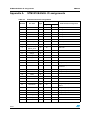
1
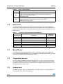
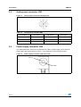
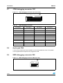
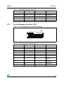
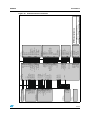
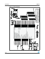
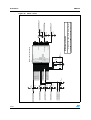
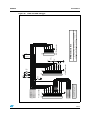
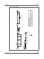
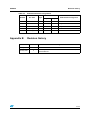
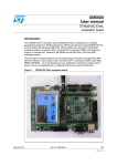
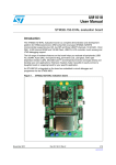
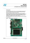
UM0426
User manual
STM3210B-EVAL
Evaluation board
Introduction
The STM3210B-EVAL is an evaluation board for STMicroelectronic’s ARMTM Cortex-M3
core-based STM32F10x 128K microcontrollers. It is designed as a complete development
environment for the STM32F10x microcontrollers with full speed USB2.0, CAN2.0A/B
compliant interface, two I2C channels, two SPI channels, three USART channels with smart
card support, internal 20KB SRAM and 128KB Flash, JTAG and SWD debugging support.
With a complete range of hardware evaluations features, the STM3210B-EVAL board is
designed to help developers evaluate all device peripherals (such as USB, motor control,
CAN, MicroSD card, Smart card, USART) and develop their own applications. Extension
connectors make it possible to easily connect a daughter board or wrapping board for a
specific application.
This user manual provides information on using the STM3210B-EVAL board and its
hardware features.
Figure 1.
May 2007
STM32F10X 128K evaluation board (STM3210B-EVAL)
Rev 2
1/42
www.st.com
UM0426
Features
●
Three 5V power supply options: power jack, USB connector or daughter board
●
Boot from user Flash, test Flash or SRAM
●
Audio play and record
●
64Mbyte MicroSD card
●
Type A and Type B smart card support
●
8Mbyte serial Flash
●
I2C/SMBus compatible serial interface temperature sensor
●
Two RS232 communication channels with support for RTS/CTS handshake on one
channel
●
IrDA transceiver
●
USB 2.0 full speed connection
●
CAN 2.0A/B compliant connection
●
Induction motor control connector
●
JTAG, SWD and trace tool support
●
240x320 TFT color LCD
●
Joystick with 4-direction control and selector
●
Reset, wakeup, tamper and user push buttons
●
4 LEDs
●
RTC with backup battery
●
Extension connector for daughter board or wrapping board
Order code
To order the STM32F10x 128K evaluation board, use the order code STM3210B-EVAL.
2/42
UM0426
Contents
Contents
1
Hardware layout and configuration . . . . . . . . . . . . . . . . . . . . . . . . . . . . . 5
Hardware configuration. . . . . . . . . . . . . . . . . . . . . . . . . . . . . . . . . . . . . . . . . . . . . . 7
2
1.1
Power supply . . . . . . . . . . . . . . . . . . . . . . . . . . . . . . . . . . . . . . . . . . . . . . . 7
1.2
Boot option . . . . . . . . . . . . . . . . . . . . . . . . . . . . . . . . . . . . . . . . . . . . . . . . . 9
1.3
Clock source . . . . . . . . . . . . . . . . . . . . . . . . . . . . . . . . . . . . . . . . . . . . . . . 10
1.4
Reset source . . . . . . . . . . . . . . . . . . . . . . . . . . . . . . . . . . . . . . . . . . . . . . 10
1.5
Audio . . . . . . . . . . . . . . . . . . . . . . . . . . . . . . . . . . . . . . . . . . . . . . . . . . . . 10
1.6
Serial flash . . . . . . . . . . . . . . . . . . . . . . . . . . . . . . . . . . . . . . . . . . . . . . . . 10
1.7
CAN . . . . . . . . . . . . . . . . . . . . . . . . . . . . . . . . . . . . . . . . . . . . . . . . . . . . . 11
1.8
RS232 . . . . . . . . . . . . . . . . . . . . . . . . . . . . . . . . . . . . . . . . . . . . . . . . . . . 11
1.9
Motor control . . . . . . . . . . . . . . . . . . . . . . . . . . . . . . . . . . . . . . . . . . . . . . 11
1.10
Smart card . . . . . . . . . . . . . . . . . . . . . . . . . . . . . . . . . . . . . . . . . . . . . . . . 12
1.11
MicroSD card . . . . . . . . . . . . . . . . . . . . . . . . . . . . . . . . . . . . . . . . . . . . . . 12
1.12
Temperature sensor . . . . . . . . . . . . . . . . . . . . . . . . . . . . . . . . . . . . . . . . . 12
1.13
Analog input . . . . . . . . . . . . . . . . . . . . . . . . . . . . . . . . . . . . . . . . . . . . . . . 12
1.14
IrDA . . . . . . . . . . . . . . . . . . . . . . . . . . . . . . . . . . . . . . . . . . . . . . . . . . . . . 13
1.15
USB . . . . . . . . . . . . . . . . . . . . . . . . . . . . . . . . . . . . . . . . . . . . . . . . . . . . . 13
1.16
Development and debug support . . . . . . . . . . . . . . . . . . . . . . . . . . . . . . . 13
1.17
Display and input devices . . . . . . . . . . . . . . . . . . . . . . . . . . . . . . . . . . . . . 14
Connectors . . . . . . . . . . . . . . . . . . . . . . . . . . . . . . . . . . . . . . . . . . . . . . . 15
2.1
USB type B connector CN1 . . . . . . . . . . . . . . . . . . . . . . . . . . . . . . . . . . . 15
2.2
CAN D-type 9-pin male connector CN2 . . . . . . . . . . . . . . . . . . . . . . . . . . 15
2.3
Analog input connector CN3 . . . . . . . . . . . . . . . . . . . . . . . . . . . . . . . . . . 16
2.4
Power supply connector CN4 . . . . . . . . . . . . . . . . . . . . . . . . . . . . . . . . . . 16
2.5
RS232 connector CN5 with RTS/CTS handshake support . . . . . . . . . . . 17
2.6
RS232 connector CN6
2.7
JTAG debugging connector CN7 . . . . . . . . . . . . . . . . . . . . . . . . . . . . . . . 18
2.8
Audio jack CN8 . . . . . . . . . . . . . . . . . . . . . . . . . . . . . . . . . . . . . . . . . . . . . 18
2.9
SWD debugging connector CN9 . . . . . . . . . . . . . . . . . . . . . . . . . . . . . . . 18
2.10
Trace debugging connector CN10 . . . . . . . . . . . . . . . . . . . . . . . . . . . . . . 19
. . . . . . . . . . . . . . . . . . . . . . . . . . . . . . . . . . . . . . 17
3/42
Contents
3
UM0426
2.11
Daughter board extension connectors CN12 and CN13 . . . . . . . . . . . . . 20
2.12
Motor control connector CN14 . . . . . . . . . . . . . . . . . . . . . . . . . . . . . . . . . 23
2.13
MicroSD connector CN15 . . . . . . . . . . . . . . . . . . . . . . . . . . . . . . . . . . . . . 25
2.14
Smartcard connector CN16 . . . . . . . . . . . . . . . . . . . . . . . . . . . . . . . . . . . 25
Schematics . . . . . . . . . . . . . . . . . . . . . . . . . . . . . . . . . . . . . . . . . . . . . . . 26
Appendix A STM3210B-EVAL IO assignments . . . . . . . . . . . . . . . . . . . . . . . . . . 38
Appendix B Revision history . . . . . . . . . . . . . . . . . . . . . . . . . . . . . . . . . . . . . . . . . 41
4/42
UM0426
1
Hardware layout and configuration
Hardware layout and configuration
The STM3210B-EVAL board is designed around a STM32F103VBT6 microcontroller in a
100-pin LQFP package.
The hardware block diagram Figure 2 shows the connections between the STM32F10x
microcontroller and peripherals (LCD, SPI Flash, USART, IrDA, USB, Audio, CAN bus, RTC,
Smart card, MicroSD card and motor control).
Figure 3 will help you locate these features on the evaluation board.
Figure 2.
Hardware block diagram
ADC
Fixed 3.3V
Power Supply
Audio Circuit
PWM
LED, Key &
Joystick
8Mbyte Flash
SPI1
GPIO
Extension
Connector for
GPIOs
64MByte
MicroSD card
LCD Module
SPI2
USART1
RS232
transceiver
USART DB9
male connector
USART2
RS232
transceiver
USART DB9
male connector
STM32F103VBT6
Temperature
sensor
I2C1
USART3
IrDA
transceiver
Motor control
connector
MC
Smart
card
Smart card
interface chip
Smart card
connector
CAN
CAN
transceiver
CAN DB9
connector
10-pin SWD
connector
20-pin JTAG
connector
20-pin future
JTAG
connector with
Trace
Debug
ADC
BNC connector
USB
USB Type B
connector
5/42
Hardware layout and configuration
Figure 3.
UM0426
STM3210B-EVAL board layout
CN12
Extension connector
U1
STM32F103VBT6
CN14
Motor control
CN15
MicroSD card
CN5
USART2
CN13
Extension connector
CN2
CAN connector
CN9
SWD
CN6
USART1
CN10
Trace
U11
IrDA
CN7
JTAG
U17
Color LCD
CN1
USB
CN8
Audio jack
CN4
5V power
RV1
Potentiometer
U17
MIC
B1
RESET
6/42
B2
WAKEUP
CN16
Smartcard
B4
Tamper
U18
Joystick
B3
General
purpose key
UM0426
Hardware layout and configuration
Hardware configuration
The following sections provide jumper settings for configuring your STM3210B-EVAL board
and peripherals.
Two types of jumpers are used on the STM3210B-EVAL board:
●
3-pin jumpers with two possible positions, for which the possible settings are presented
in schematics in the following sections
●
2-pin jumpers with two possible settings: Fitted– the circuit is closed, and Not fitted–
the circuit is open (see Figure 4.)
Figure 4.
Settings for two-pin jumpers
Not fitted
1.1
Fitted
Power supply
The STM3210B-EVAL board is designed to be powered by 5V DC power supply and to be
protected by PolyZen U6 in case of incorrect power supply configuration. It is possible to
configure the evaluation board to use any of the following sources for the power supply.
●
5V DC power adapter connected to CN4, the power supply jack labeled “PSU” (for
Power Supply Unit) on the silkscreen
●
5V DC power with 500mA limitation from CN1, the type-B USB connector on the
evaluation board labeled “USB” on the silkscreen
●
5V DC power from both CN12 and CN13, the daughter board extension connectors
labeled “DTB” (for Daughter Board) on the silkscreen
The power supply is configured by setting the related jumpers JP4, JP9 and JP11 as
described in Table 1.
7/42
Hardware layout and configuration
Table 1.
Jumper
UM0426
Power related jumpers
Description
JP4 is used to select one of the three possible power supply resources.
For power supply from the power supply jack (CN4) to the STM3210B-EVAL only,
JP4 is set as shown below (default setting):
PSU
DTB
USB
For power supply from the daughter board connectors (CN12 and CN13) to the
STM3210B-EVAL only, JP4 is set as shown below:
PSU
DTB
USB
JP4
For power supply from USB (CN1) to the STM3210B-EVAL only, JP4 is set as shown
below:
PSU
DTB
USB
For power supply from power supply jack (CN4) to both the STM3210B-EVAL board
and to a daughter board connected on CN12 and CN13, JP4 is set as shown below.
The daughter board must not have its own power supply connected.
PSU
DTB
USB
JP9
Measures the consumption of VDD and VDDA.
Default setting: Fitted
Vbat is connected to 3.3V power when JP11 is set as shown below (default setting):
1 2 3
JP11
Vbat is connected to battery when JP11 is set as shown below:
1 2 3
The LED LD5 is lit when the STM3210B-EVAL board is powered correctly.
8/42
UM0426
Boot option
The STM3210B-EVAL board is able to boot from:
●
Embedded user Flash
●
System memory with boot loader for ISP
●
Embedded SRAM for debugging
The boot option is configured by setting the switches SW1 and SW2 as shown in Table 2.
The two possible positions of these micro switches are shown in Figure 5.
Switch positions
>0
Figure 5.
1<
Switch in
position “1”
1<
>0
SW2
Boot 0
>0
1<
STM3210B-EVAL boots from system memory when SW1
and SW2 are set as shown to the right.
Boot 0 = 1, Boot 1 = 0
>0
SW2
STM3210B-EVAL boots from embedded SRAM when
SW1 and SW2 are set as shown to the right.
Boot 0 = 1, Boot 1 = 1
1<
SW1
SW2
Boot 0
STM3210B-EVAL boots from user Flash when SW2 is set
as shown to the right (default setting).
In this configuration, the position of SW1 doesn’t affect the
boot process.
Boot 0 = 0, Boot 1 = X
Switch configuration
SW2
Boot 0
Boot from
SW1
Boot 1
Switch
Boot switches
SW1
Boot 1
Table 2.
Switch in
position “0”
SW1
Boot 1
1.2
Hardware layout and configuration
9/42
Hardware layout and configuration
1.3
UM0426
Clock source
Two clock sources are available on the STM3210B-EVAL board for the STM32F10X
microcontroller and RTC.
1.4
●
X1, 32KHz crystal for embedded RTC
●
X2, 8MHz crystal with socket for the STM32F10X microcontroller. It can be removed
from the socket when the internal RC clock is used.
Reset source
The reset signal of the STM3210B-EVAL board is active low and the reset sources include:
●
Reset button B1
●
Debugging tools from connector CN7, CN9 and CN10
●
Daughter board from CN13
Table 3.
Reset jumper
Jumper
JP10
1.5
Description
Enables reset of the STM32F10X microcontroller embedded JTAG TAP controller
each time a system reset occurs. JP10 connects the TRST signal from the JTAG
connection with the system reset signal RESET#.
Default setting: Not fitted
Audio
The STM3210B-EVAL board supports both audio recording and playback. This can be
disabled or enabled by setting the jumpers JP6 and JP7. The audio volume can be adjusted
using the potentiometer RV2, and the microphone amplifier gain can be adjusted using the
potentiometer RV3.
Table 4.
Audio jumpers
Jumper
1.6
Description
JP6
Audio power amplifier TS4871 is forced into standby mode when JP6 is not fitted.
Default setting: Fitted
JP7
Microphone pre-amplifier MAX4061 is forced into shutdown mode when JP7 is fitted.
Default setting: Not fitted
Serial flash
A 64Mbit serial flash connected to SPI1 of the STM32F10X microcontroller shares the same
SPI port with the MicroSD card using a different chip select signal. Serial Flash Chip select
is managed by the standard IO port PA4.
10/42
UM0426
1.7
Hardware layout and configuration
CAN
The STM3210B-EVAL board supports CAN 2.0A/B compliant CAN bus communication
based on 3.3V CAN transceiver. The high-speed mode, standby mode and slope control
mode are available and selected by setting JP2.
Table 5.
CAN jumpers
Jumper
Description
CAN transceiver functions in standby mode when JP2 is set as shown below:
1 2 3
JP2
CAN transceiver functions in high-speed mode when JP2 is set as shown below:
1 2 3
CAN transceiver functions in slope control mode when JP2 is not fitted.
(Default setting)
JP3
1.8
CAN terminal resistor is enabled when JP3 is fitted.
Default setting: Not fitted
RS232
Two Type D 9-pin connectors, CN6 (USART1) and CN5 (USART2) are available on the
STM3210B-EVAL board. The USART1 connector is connected to the RS232 transceiver
U10, and the USART2 connector with RTS/CTS handshake signal support is connected to
the RS232 transceiver U9.
1.9
Motor control
The STM3210B-EVAL board supports induction motor control via a 34-pin connector, CN14,
which provides all required control and feedback signals to and from a motor power-drive
board. Available signals on this connector include emergency stop, motor speed, 3-phase
motor current, bus voltage, heatsink temperature coming from the motor drive board and 6
channels of PWM control signals going to the motor drive circuit.
Special motor current sampling operation is enabled by setting jumper JP8.
11/42
Hardware layout and configuration
Table 6.
1.10
UM0426
Motor control jumpers
Jumper
Description
JP8
Enables special motor current sampling operation when JP8 is fitted (PD2 connected
to PB0). The IO pins PD2 and PB0 are disconnected and can be used by the
daughter board when JP8 is not fitted.
Default setting: Fitted
JP12
JP12 must be open when the digital encoder signal comes from pin31 of CN14. It
must be closed when an analog signal comes from pin31 of CN14.
Default setting: Not fitted (open)
Smart card
The STMicroelectronics smart card interface device ST8024 is used on the STM3210BEVAL board for asynchronous 3V and 5V smart cards. It performs all supply protection and
control functions based on the connections with the STM32F10X microcontroller, which are
listed inTable 7.
Table 7.
Connection between ST8024 and STM32F10X
ST8024 signals
1.11
Description
Connect to
STM32F10X
5V/3V
Smart card power supply selection pin
PD11
I/OUC
MCU data I/O line
PB10
XTAL1
Crystal or external clock input
PB12
OFF
Detect presence of a card, Interrupt to MCU
PE14
RSTIN
Card reset input from MCU
PB11
CMDVCC
Start activation sequence input (active low)
PE7
MicroSD card
The 64Mbyte MicroSD card, SMS064FF, which is connected to SPI1 of the STM32F10x
microcontroller (shared with serial Flash), is available on the board. The MicroSD card chip
selection is managed by the standard IO port PC12.
1.12
Temperature sensor
One I2C interface temperature sensor STLM75 (–55°C to +125°C), which is connected to
I2C1 of the STM32F10x microcontroller, is available on the board. Two discrete N-channel
enhancement MOS-FETs are used to demonstrate how different voltage level devices can
be connected to the same I2C bus.
1.13
Analog input
One BNC connector, CN3, is connected to PC1, the ADC channel 11 of the STM32F10x
microcontroller as an external analog input.
12/42
UM0426
1.14
Hardware layout and configuration
IrDA
IrDA communication is supported by the IrDA transceiver U11, which is connected to
USART3 of the STM32F10x microcontroller. It can be enabled or disabled by setting the
jumper JP5.
Table 8.
IrDA jumpers
Jumper
JP5
1.15
Description
Enables/disables the IrDA transceiver. IrDA is enabled when JP5 is fitted, and
disabled when JP5 is not fitted.
Default setting: Fitted
USB
The STM3210B-EVAL board supports USB2.0 compliant full-speed communication via a
USB type B connector (CN1). The evaluation board can be powered by this USB connection
at 5V DC with a 500mA current limitation.
USB disconnect simulation can be implemented by disconnecting a 1.5K pull-up register
from the USB+ line. The USB disconnect simulation feature is enabled by setting JP1.
Table 9.
Jumper
USB jumpers
Description
USB 1.5K pull-up register is always connected to USB+ line when JP1 is set as shown
below (default setting):
123
JP1
USB 1.5K pull-up register can be disconnected by software from the USB+ line when
JP1 is set as shown below. In this case USB connect/disconnect features are
managed by the standard IO port PD9.
123
1.16
Development and debug support
The following debug connectors are available on the STM3210B-EVAL board:
●
CN7, an industry standard 20-pin JTAG interface connector for connection of
debugging/programming tools for ARM7 and ARM9 core-based devices.
●
CN9, a 10-pin SWD debug connector that supports the new Serial Wire Debug feature
of ARM Cortex-M3 devices.
●
CN10, a 20-pin connector for legacy and future JTAG tools that are compliant with ARM
CoreSight.
13/42
Hardware layout and configuration
1.17
UM0426
Display and input devices
The 240x320 TFT color LCD (U17) and 4 general purpose LEDs (LD1, 2, 3, 4) are available
as display devices. A 4-direction joystick with selection key, general purpose pushbutton
(B3), wakeup button (B2) and tamper detection button (B4) are available as input devices.
The STM3210B-EVAL board also supports a second optional 122x32 graphic LCD that can
be mounted on the U19 connector. The graphic LCD is not provided.
Table 10.
LCD modules
Graphic LCD U17 (default)
Pin on
U17
14/42
Description
Pin connection
Character LCD U19 (optional)
Pin on
U19
Description
Pin connection
1
CS
PB2
1
Vss
GND
2
SCL
PB13
2
Vcc
+3.3V
3
SDI
PB15
3
VO
-
4
RS
PD7
4
CLK
PB13
5
WR
PD15
5
SID
PB15
6
RD
GND
6
CS
PB2
7
SDO
PB14
7
A
+5V
8
RESET#
RESET#
8
K
GND
9
VDD
+3V3
10
VCI
+3V3
11
GND
GND
12
GND
GND
13
BL_VDD
+3V3
14
BL_Control
PA8
15
BL_GND
GND
16
BL_GND
GND
UM0426
Connectors
2
Connectors
2.1
USB type B connector CN1
Figure 6.
USB type B connector CN1 (front view)
Table 11.
USB type B connector (CN1)
Pin number
2.2
Description
1
VBUS(power)
2
DM
3
DP
Pin number
Description
4
GND
5, 6
Shield
CAN D-type 9-pin male connector CN2
Figure 7.
CAN D-type 9-pin male connector CN2 (front view)
Table 12.
CAN D-type 9-pin male connector (CN2)
Pin number
1, 4, 8, 9
2
Description
NC
CANL
Pin number
7
3, 5, 6
Description
CANH
GND
15/42
Connectors
2.3
UM0426
Analog input connector CN3
Figure 8.
Analog input connector CN3 (top view)
1
2
5
4
Table 13.
Analog input connector CN3
Pin number
2.4
3
Description
Pin number
Description
1
GND
4
GND
2
GND
5
Analog input/PC1
3
GND
Power supply connector CN4
The STM3210B-EVAL board can be powered from a DC 5V power supply via the external
power supply jack (CN4) shown in Figure 9. The central pin of CN4 must be positive.
Figure 9.
Power supply connector CN4 (front view)
DC +5V
GND
16/42
UM0426
2.5
Connectors
RS232 connector CN5 with RTS/CTS handshake support
Figure 10. RS232 connector CN5 with RTS/CTS handshake support (front view)
Table 14.
RS232 connector CN5 with full modem control support
Pin number
2.6
Description
Pin number
Description
1
NC
6
Connect to Pin 4
2
USART2_RXD
7
USART2_RTS
3
USART2_TXD
8
USART2_CTS
4
Connect to Pin 6
9
NC
5
GND
RS232 connector CN6
Figure 11. RS232 connector CN6 (front view)
Table 15.
RS232 connector CN6
Pin number
Description
Pin number
Description
1
NC
6
Connect to Pin 4
2
USART1_RXD
7
Connect to Pin 8
3
USART1_TXD
8
Connect to Pin 7
4
Connect to Pin 6
9
NC
5
GND
17/42
Connectors
2.7
UM0426
JTAG debugging connector CN7
Figure 12. JTAG debugging connector CN7 (front view)
Table 16.
3
1
20 18 16 14 12 10 8 6
4
2
JTAG debugging connector
Pin number
2.8
19 17 15 13 11 9 7 5
Description
Pin number
Description
1
3.3V power
2
3.3V power
3
TRST
4
GND
5
TDI
6
GND
7
TMS
8
GND
9
TCK
10
GND
11
RTCK
12
GND
13
TDO
14
GND
15
RESET#
16
GND
17
DBGRQ
18
GND
19
DBGACK
20
GND
Audio jack CN8
A 3.5mm mono audio jack CN8 is available on the STM3210B-EVAL board. The speaker
U12 is bypassed when earphones are plugged into CN8.
2.9
SWD debugging connector CN9
Figure 13. SWD debugging connector CN9 (top view)
18/42
9 7 5
3
1
10 8 6
4
2
UM0426
Connectors
Table 17.
SWD debugging connector (CN9)
Pin number
2.10
Description
Pin number
Description
1
+3V3
2
SWDIO/PA13
3
GND
4
SWCLK/PA14
5
GND
6
SWO/PB3
7
GND
8
TDI/PA15
9
GND
10
RESET#
Trace debugging connector CN10
Figure 14. Trace debugging connector CN10 (front view)
Table 18.
19 17 15 13 11 9 7 5
3
1
20 18 16 14 12 10 8 6
4
2
Trace debugging connector (CN10)
Pin number
Description
Pin number
Description
1
3.3V power
2
TMS/PA13
3
GND
4
TCK/PA14
5
GND
6
TDO/PB3
7
GND
8
TDI/PA15
9
GND
10
RESET#
11
GND
12
TraceCLK/PE2
13
GND
14
TraceD0/PE3 or
SWO/PB3
15
GND
16
TraceD1/PE4 or
nTRST/PB4
17
GND
18
TraceD2/PE5
19
GND
20
TraceD3/PE6
19/42
Connectors
2.11
UM0426
Daughter board extension connectors CN12 and CN13
Two 50-pin male headers, CN12 and CN13, can be used to connect a daughter board or
standard wrapping board to the STM3210B-EVAL board. A total of 80 GPI/Os are available
on these connectors. Each pin on CN12 and CN13 can be used by a daughter board after
disconnecting it from the corresponding function block on the STM3210B-EVAL board.
Refer to Table 19 and Table 20 for details.
Table 19.
20/42
Daughter board extension connector CN12
How to disconnect from function block on
STM3210B-EVAL board
Pin
Description
Alternate function
1
GND
-
3
PC1
MC connector pin 15
Disconnect STM3210B-EVAL board from motor
power drive board
5
PC3
MC connector pin 19
Disconnect STM3210B-EVAL board from motor
power drive board
7
PA1
MC connector pin 33
Disconnect STM3210B-EVAL board from motor
power drive board
9
PA3
MC connector pin 14
Disconnect STM3210B-EVAL board from motor
power drive board
11
PA4
SPI Flash
13
PA6
15
PC4
17
PB0
19
GND
-
-
21
PE7
Smart card
-
23
PE9
MC connector pin 3
Disconnect STM3210B-EVAL board from motor
power drive board
25
PE11
MC connector pin 7
Disconnect STM3210B-EVAL board from motor
power drive board
27
PE13
MC connector pin 11
Disconnect STM3210B-EVAL board from motor
power drive board
29
PE15
MC connector pin 1
Remove R53
31
NC
-
33
PB10
Smart card
35
PB13
LCD
-
37
PB15
LCD
-
39
GND
-
-
41
PD9
USB
43
PD11
Smart card
45
PD13
MC connector pin 23
-
Remove R63
SPI Flash & MicroSD
Remove R65 and R82
card
Potentiometer RV1
Remove R80
MC connector pin 27 JP8 is not fitted
Remove R115
Disconnect JP1
Disconnect STM3210B-EVAL board from motor
power drive board
UM0426
Connectors
Table 19.
Daughter board extension connector CN12 (continued)
How to disconnect from function block on
STM3210B-EVAL board
Pin
Description
Alternate function
47
PD15
LCD
-
49
D5V
-
-
2
PC0
MC connector pin 26
Disconnect STM3210B-EVAL board from motor
power drive board
4
PC2
MC connector pin 17
Disconnect STM3210B-EVAL board from motor
power drive board
6
PA0
Disconnect STM3210B-EVAL board from motor
MC connector pin 31 power drive board
& wakeup button
Remove R85
8
PA2
Joystick Down
10
GND
-
12
PA5
SPI Flash & MicroSD
card
14
PA7
SPI Flash & MicroSD
card
16
PC5
Microphone
18
PB1
MC connector pin 29
20
PB2
BOOT & LCD
22
PE8
MC connector pin 5
Disconnect STM3210B-EVAL board from motor
power drive board
24
PE10
MC connector pin 9
Disconnect STM3210B-EVAL board from motor
power drive board
26
PE12
MC connector pin 13
Disconnect STM3210B-EVAL board from motor
power drive board
28
PE14
Smart card
30
GND
-
-
32
NC
-
-
34
PB11
Smart card
-
36
PB12
Smart card
-
38
PB14
LCD
40
PD8
Joystick Up
42
PD10
MC connector pin 21
44
PD12
Joystick selection
46
PD14
MC connector pin 34
Remove R73
-
Remove R71
Disconnect STM3210B-EVAL board from motor
power drive board
-
Remove R117
Remove LCD module
Remove R76
Disconnect STM3210B-EVAL board from motor
power drive board
Remove R72
Disconnect STM3210B-EVAL board from motor
power drive board
21/42
Connectors
UM0426
Table 19.
How to disconnect from function block on
STM3210B-EVAL board
Pin
Description
Alternate function
48
+3V3
-
-
50
GND
-
-
Table 20.
22/42
Daughter board extension connector CN12 (continued)
Daughter board extension connector CN13
How to disconnect from component on
STM3210B-EVAL board
Pin
Description
Alternate function
1
GND
-
-
3
NC
5
PE6
Debug TraceD3
-
7
PE4
Debug TraceD1
-
9
PC13
Tamper key
-
11
RESET#
RESET# button
-
13
PE1
Joystick Left
Remove R74
15
PB9
User button
Remove R78
17
PB7
Temperature sensor
Remove R114
19
D5V
-
21
PB4
Debug nTRST
23
NC
-
25
PD6
USART2
Remove R77
27
PD4
USART2
-
29
PD3
USART2
Remove R79
31
PD1
CAN_TX
-
33
PC12
MicroSD card
35
PC10
IrDA
-
37
PA14
Debug TCK
-
39
GND
-
-
41
PA12
USB
-
43
PA10
USART1_RX
45
PA8
LCD
-
47
PC8
LED3
Remove R6
49
PC6
LED1
Remove R8
2
NC
4
PC13
Tamper button
Remove R62
6
PE5
Debug TraceD2
-
8
PE3
Debug TraceD0
-
JP10 is not fitted
-
Remove R81
Remove R70
UM0426
Connectors
Table 20.
2.12
Daughter board extension connector CN13 (continued)
How to disconnect from component on
STM3210B-EVAL board
Pin
Description
Alternate function
10
GND
-
-
12
PE2
Debug trace CLK
-
14
PE0
Joystick Right
Remove R75
16
PB8
Speaker
Unfitted JP6
18
PB6
Temperature sensor
Remove R113
20
PB5
Temperature sensor
Remove R112
22
PB3
Debug SWO
-
24
NC
-
-
26
PD7
LCD
-
28
PD5
USART2
-
30
GND
-
-
32
PD2
MC connector pin 27
34
PD0
CAN_RX
Remove R116
36
PC11
IrDA
Remove R64
38
PA15
Debug TDI
-
40
PA13
Debug TMS
-
42
PA11
USB
-
44
PA9
USART1_TX
-
46
PC9
LED4
Remove R5
48
PC7
LED2
Remove R7
50
GND
-
Disconnect STM3210B-EVAL board from motor
power drive board
-
Motor control connector CN14
Figure 15. Motor control connector CN14 (top view)
33 31 29 27 25 23 21 19 17 15 13 11 9 7 5
3
1
34 32 30 28 26 24 22 20 18 16 14 12 10 8 6
4
2
23/42
Connectors
UM0426
Table 21.
Motor control connector CN14
Description
Pin of
Pin number Pin number
Pin of
STM32F10X
on CN1
on CN1
STM32F10x
EMERGENCY
STOP
PE15
1
2
GND
PWM-UH
PE9
3
4
GND
PWM-UL
PE8
5
6
GND
PWM-VH
PE11
7
8
GND
PWM-VL
PE10
9
10
GND
PWM-WH
PE13
11
12
GND
PWM-WL
PE12
13
14
PHASE A
CURRENT
PC1
15
16
GND
PHASE B
CURRENT
PC2
17
18
GND
PHASE C
CURRENT
PC3
19
20
GND
NTC BYPASS
RELAY
PD10
21
22
GND
DISSIPATIVE
BRAKE PWM
PD13
23
24
GND
25
26
+5V power
24/42
Description
PA3
PC0
BUS VOLTAGE
Heatsink
temperature
PFC SYNC
PD2/PB0
27
28
3.3V power
PFC PWM
PB1
29
30
GND
Encoder A
PA0
31
32
GND
Encoder B
PA1
33
34
PD14
Encoder Index
UM0426
2.13
Connectors
MicroSD connector CN15
Figure 16. MicroSD connector CN15 (top view)
Table 22.
MicroSD connector CN15
Pin number
2.14
Description
Pin number
Description
1
Reserved
5
SCLK/PA5
2
CS/PC12
6
Vss/GND
3
DI/PA7
7
DO/PA6
4
VDD
8, 9
Reserved
Smartcard connector CN16
Figure 17. Smartcard connector CN16 (top view of connector underneath PCB)
25/42
Schematics
UM0426
Table 23.
Smartcard connector CN16
Pin number
3
Description
Pin number
Description
1
VCC
5
GND
2
RST
6
NC
3
CLK
7
I/O
4
NC
8
NC
17
Card presence
detection pin
18
Card presence
detection pin
Schematics
This section provides design schematics for the STM3210B-EVAL key features to help you
implement these features in your own application designs.
This section includes:
26/42
●
Overall schematics for the board, see Figure 18
●
MCU connections, see Figure 19
●
EEPROM, USB, LED, CAN and temperature sensor, see Figure 20
●
USART1, USART2, IrDA, see Figure 21
●
Audio amplifier and micro amplifier, see Figure 22
●
Joystick, LCD, tamper button, wakeup button, user button, see Figure 23
●
Smart card and MicroSD card, Figure 24
●
Motor control, Figure 25
●
JTAG, SWD debugger, see Figure 26
●
Power supply, see Figure 27
●
Extension connectors, see Figure 28
RESET#
PE[0..15]
PD[0..15]
PC[0..15]
PB[0..15]
PA[0..15]
JOY_SEL
JOY_DOWN
JOY_LEFT
JOY_RIGHT
JOY_UP
Anti_Tamper
MC_EnA/WAKEUP
User_Button
RESET#
LCD_backlight
LCD_DO
LCD_WR
LCD_RS
LCDI_DI
LCD_CLK
LCD_CS
U_Extension
Extension.SchDoc
U_Power
Power.SchDoc
MIC_IN
Audio_PWM
TDI
RESET#
TRST
TMS/SWDIO
TCK/SWCLK
TDO/SWO
TRACE_CK
TRACE_D0
TRACE_D1
TRACE_D2
TRACE_D3
U_LCD&Joystick
LCD&Joystick.SchDoc
U_JTAG&SWD
JTAG&SWD.SchDoc
U_Audio
Audio.SchDoc
RESET#
PE[0..15]
PD[0..15]
PC[0..15]
PB[0..15]
PA[0..15]
LCD_backlight
LCD_DO
LCD_WR
LCD_RS
LCDI_DI
LCD_CLK
LCD_CS
User_Button
JOY_SEL
JOY_DOWN
JOY_LEFT
JOY_RIGHT
JOY_UP
Anti_Tamper
TRST
TMS/SWDIO
TCK/SWCLK
TDO/SWO
TRACE_CK
TRACE_D0
TRACE_D1
TRACE_D2
TRACE_D3
TDI
MIC_IN
Audio_PWM
U_MCU
MCU.SchDoc
USART1_TX
USART1_RTS
USART1_RX
USART1_CTS
IrDA_RX
IrDA_TX
USART0_RX
USART0_TX
MicroSDCard_CS
SmartCard_3/5V
SmartCard_IO
SmartCard_RST
SmartCard_CLK
SmartCard_CMDVCC
SmartCard_OFF
SPI1_NSS
SPI1_SCK
SPI1_MOSI
SPI1_MISO
USB_DM
USB_DP
USB_Disconnect
TemperatureSensor_SCL
TemperatureSensor_SDA
TemperatureSensor_INT
CAN_TX
CAN_RX
LED4
LED3
LED2
LED1
Potentiometer
MC_PFCsync1
MC_PFCsync2
MC_WL
MC_VH
MC_VL
MC_UH
MC_UL
MC_WH
MC_NTC
MC_DissipativeBrake
MC_PFCpwm
MC_EmergencySTOP
MC_EnIndex
MC_BusVoltage
MC_HeatsinkTemperature
MC_EnB
MC_EnA/WAKEUP
MC_CurrentC
MC_CurrentB
MC_CurrentA/BNC
USART1_TX
USART1_RTS
USART1_RX
USART1_CTS
IrDA_RX
IrDA_TX
USART0_RX
USART0_TX
U_RS232&IrDA
RS232&IrDA.SchDoc
SmartCard_3/5V
SmartCard_IO
SmartCard_RST
SmartCard_CLK
SmartCard_CMDVCC
SmartCard_OFF
SPI1_MISO
SPI1_MOSI
SPI1_SCK
MicroSDCard_CS
U_SD&Smart Card
SD&Smart Card.SchDoc
SPI1_NSS
SPI1_SCK
SPI1_MOSI
SPI1_MISO
USB_DM
USB_DP
USB_Disconnect
TemperatureSensor_SCL
TemperatureSensor_SDA
TemperatureSensor_INT
CAN_TX
CAN_RX
LED4
LED3
LED2
LED1
Potentiometer
MC_CurrentA/BNC
U_Peripherals
Peripherals.SchDoc
MC_PFCsync1
MC_PFCsync2
MC_WL
MC_VH
MC_VL
MC_UH
MC_UL
MC_WH
MC_NTC
MC_DissipativeBrake
MC_PFCpwm
MC_EmergencySTOP
MC_EnIndex
MC_BusVoltage
MC_HeatsinkTemperature
MC_EnB
MC_EnA/WAKEUP
MC_CurrentC
MC_CurrentB
MC_CurrentA/BNC
U_MotorCtrl
MotorCtrl.SchDoc
Rev: B.1(PCB.SCH)
Date: 2007-05-02
STM32F10X-128K-EVAL
Number:MB525
Title:
STMicroelectronics
Sheet 1 of
11
UM0426
Schematics
Figure 18. Evaluation board schematics
27/42
2
3
100nF
C5
2
10K
R2
+3V3
R1
1M
+3V3
SW2
R87
100K
TDO/SWO
TRST
TemperatureSensor_INT
TemperatureSensor_SCL
TemperatureSensor_SDA
Audio_PWM
User_Button
SmartCard_IO
SmartCard_RST
SmartCard_CLK
LCD_CLK
LCD_DO
LCDI_DI
MC_PFCsync1
MC_PFCpwm
USART0_TX
USART0_RX
USB_DM
USB_DP
TMS/SWDIO
TCK/SWCLK
TDI
X2
8MHz (with socket)
4
RESET
MCO
100K
R86
1
B1
20pF
C4
C3
20pF
RESET#
3
+3V3
1 SW1
LCD_CS
LCD_backlight
2
TP8
MC_EnA/WAKEUP
MC_EnB
MC_EnIndex
MC_BusVoltage
SPI1_NSS
SPI1_SCK
SPI1_MISO
SPI1_MOSI
1
28/42
3
35
36
37
89
90
91
92
93
95
96
47
48
51
52
53
54
PB0
PB1
PB2
PB3
PB4
PB5
PB6
PB7
PB8
PB9
PB10
PB11
PB12
PB13
PB14
PB15
BOOT0
73
94
OSC_IN 12
OSC_OUT 13
RESET# 14
23
24
25
26
29
30
31
32
67
68
69
70
71
72
76
77
PA0
PA1
PA2
PA3
PA4
PA5
PA6
PA7
PA8
PA9
PA10
PA11
PA12
PA13
PA14
PA15
C57
100nF
STM32F103VBH6
Not connected
BOOT0
OSC_IN
OSC_OUT
NRST
C58
100nF
C59
100nF
C60
100nF
VDD
PD15
PD14
PD13
PD12
PD11
PD10
PD9
PD8
PD7
PD6
PD5
PD4
PD3
PD2
PD1
PD0
PE15
PE14
PE13
PE12
PE11
PE10
PE9
PE8
PE7
PE6
PE5
PE4
PE3
PE2
PE1
PE0
46
45
44
43
42
41
40
39
38
5
4
3
2
1
98
97
PC15
PC14
PC13
PC12
PC11
PC10
PC9
PC8
PC7
PC6
PC5
PC4
PC3
PC2
PC1
PC0
62
61
60
59
58
57
56
55
88
87
86
85
84
83
82
81
9
8
7
80
79
78
66
65
64
63
34
33
18
17
16
15
GND GND GND GND
TP12 TP13 TP14 TP15
PE15
PE14
PE13
PE12
PE11
PE10
PE9
PE8
PE7
PE6
PE5
PE4
PE3
PE2
PE1
PE0/TIM4_ETR
PD15
PD14
PD13
PD12
PD11
PD10
PD9
PD8
PD7
PD6
PD5
PD4
PD3
PD2/TIM3_ETR
PD1
PD0
PC15-OSC32_OUT
PC14-OSC32_IN
PC13-ANTI_TAMP
PC12
PC11
PC10
PC9
PC8
PC7
PC6
PC5/ADC_IN15
PC4/ADC_IN14
PC3/ADC_IN13
PC2/ADC_IN12
PC1/ADC_IN11
PC0/ADC_IN10
C61
100nF
PB0/ADC_IN8/TIM3_CH3
PB1/ADC_IN9/TIM3_CH4
PB2 / BOOT1
PB3/JTDO
PB4/JTRST
PB5/I2C1_SMBAl
PB6/I2C1_SCL/TIM4_CH1
PB7/I2C1_SDA/TIM4_CH2
PB8/TIM4_CH3
PB9/TIM4_CH4
PB10/I2C2_SCL/USART3_TX
PB11/I2C2_SDA /USART3_RX
PB12/SPI2_NSS /I2C2_SMBAl/USART3_CK /TIM1_BKIN
PB13/SPI2_SCK /USART3_CTS /TIM1_CH1N
PB14/SPI2_MISO /USART3_RTS /TIM1_CH2N
PB15/SPI2_MOSITIM1_CH3N
PA0-WKUP/USART2_CTS/ADC_IN0/TIM2_CH1_ETR
PA1/USART2_RTS/ADC_IN1/TIM2_CH2
PA2/USART2_TX/ADC_IN2/TIM2_CH3
PA3/USART2_RX/ADC_IN3/TIM2_CH4
PA4/SPI1_NSS/USART2_CK/ADC_IN4
PA5/SPI1_SCK/ADC_IN5
PA6/SPI1_MISO/ADC_IN6/TIM3_CH1
PA7/SPI1_MOSI/ADC_IN7/TIM3_CH2
PA8/USART1_CK/TIM1_CH1/MCO
PA9/USART1_TX/TIM1_CH2
PA10/USART1_RX/TIM1_CH3
PA11 / USART1_CTS/CANRX / USBDM (2)/TIM1_CH4
PA12 / USART1_RTS/CANTX / USBDP (2)/TIM1_ETR
PA13/JTMS-SWDAT
PA14/JTCK-SWCLK
PA15/JTDI
U1A
C1
10pF
1
2
C2
10pF
PB0
PB1
PB2
PB3
PB4
PB5
PB6
PB7
PB8
PB9
PB10
PB11
PB12
PB13
PB14
PB15
PA0
PA1
PA2
PA3
PA4
PA5
PA6
PA7
PA8
PA9
PA10
PA11
PA12
PA13
PA14
PA15
+3V3
+3V3
2
PB[0..15]
PB[0..15]
PD15
PD14
PD13
PD12
PD11
PD10
PD9
PD8
PD7
PD6
PD5
PD4
PD3
PD2
PD1
PD0
PD[0..15]
Rev: B.1(PCB.SCH)
Date: 2007-05-02
Sheet 2 of
STM32F10X-128K-EVAL MCU
Number:MB525
Title:
PE15
PE14
PE13
PE12
PE11
PE10
PE9
PE8
PE7
PE6
PE5
PE4
PE3
PE2
PE1
PE0
74
99
49
27
10
20
19
PE[0..15]
STM32F103VBH6
PC[0..15]
6
VSS_2
VSS_3
VSS_1
VBAT VSS_4
VSS_5
VREFVSSA
10nF
C77
VREF+
VDDA
VDD_5
VDD_4
VDD_1
VDD_2
VDD_3
U1B
VREF
TP11
PD[0..15]
PC[0..15]
PA[0..15]
PC15
PC14
PC13
PC12
PC11
PC10
PC9
PC8
PC7
PC6
PC5
PC4
PC3
PC2
PC1
PC0
Vbat
21
22
11
28
50
75
100
VREF+
C56
10nF
VDD
JP11
BT1
CR1220 holder
1
3
C55
10uF
47
VDDA
R83
L1
BEAD
VDD
PA[0..15]
JP9
STMicroelectronics
MC_EmergencySTOP
SmartCard_OFF
MC_WH
MC_WL
MC_VH
MC_VL
MC_UH
MC_UL
SmartCard_CMDVCC
TRACE_D3
TRACE_D2
TRACE_D1
TRACE_D0
TRACE_CK
JOY_LEFT
JOY_RIGHT
LCD_WR
JOY_DOWN
MC_DissipativeBrake
JOY_SEL
SmartCard_3/5V
MC_NTC
USB_Disconnect
JOY_UP
LCD_RS
USART1_RX
USART1_TX
USART1_RTS
USART1_CTS
MC_PFCsync2
CAN_TX
CAN_RX
Anti_Tamper
MicroSDCard_CS
IrDA_RX
IrDA_TX
LED4
LED3
LED2
LED1
MIC_IN
Potentiometer
MC_CurrentC
MC_CurrentB
MC_CurrentA/BNC
MC_HeatsinkTemperature
R15
0
4
3
X1
MC306-G-06Q-32.768 (manufacturer JFVNY)
11
PE[0..15]
R84
0
VREF-
Schematics
UM0426
Figure 19. MCU connections
VB334
1
2
3
4
5
CN3
600
R5
600
R6
600
R7
600
0
0
LD4
red
1
LD3
red
1
LD2
red
1
LD1
red
1
PC4
0
R80
2
PB7 R114
PB6 R113
PB5 R112
0 TS_SDA
0 TS_SCL
0 TS_INT
Potentiometer
TemperatureSensor_SDA
TemperatureSensor_SCL
TemperatureSensor_INT
Potentiometer
PC1
PC9
PC8
PC7
PC6
R8
PA4 R63
PA6 R65
2
2
2
2
1
S
G
S
3
D
TR2
BSS123
1
G
+3V3
SPI Flash
M25P64-VME6G
R88 R89 R90
4K7 4K7 4K7
RV1
10K
BNC connector +3V3
MC_CurrentA/BNC
LED4
LED3
LED2
LED1
SPI1_SCK
SPI1_MOSI
SPI1_NSS
SPI1_MISO
6
5
4
3
D
3
TR1
BSS123
+3V3
PA5
PA7
1
2
3
4
STLM75M2E
SDA VDD
SCL
A0
OS/INT A1
GND
A2
U4
8
7
6
5
C10
100nF
0
+3V3
U5V
+3V3
PD0 R116
PD1
R3
C9 1M
4.7nF
U5V
Temperature sensor
R16 R17
4K7 4K7
+5V
CAN_RX
CAN_TX
USB
CN1
USB-typeB connector
1
VCC
2
D3
D+
4
GND
0
SHELL
0
SHELL
100nF
C8
1
2
3
4
8
7
6
5
2
JP2
2K2
R91
R10
R9
+3V3
R18
47K
+3V3
U5V
C6
100nF
22
22
JP1
3
1
PD9
R118
0
1
6
2
7
3
8
4
9
5
Rev: B.1(PCB.SCH)
Date: 2007-05-02
Sheet 3 of
11
CN2
DB9-male CAN connector
USB_Disconnect
USB_DP
USB_DM
+3V3
R21
do not fit
R19
120
JP3
2
PA12
PA11
STM32F10X-128K-EVAL Peripherals
Number:MB525
Title:
STMicroelectronics
CAN
10K
1
1.5K
R12
6
5
4
R4
RS
CANH
CANL
Vref
9013
T2
SN65HVD230
D
GND
VCC
R
U5
3
36K
R14
1
USBLC6-2P6
I/O1
I/O1
GND Vbus
I/O2
I/O2
U2
10K 9013
R13
3 T1
1
2
3
2
100nF U3
7
HOLD
C
8
D
VCC
1
VSS
S
2
Q
W
2
R11
10K
3
1
2
C7
2
1
+3V3
3
+3V3
UM0426
Schematics
Figure 20. EEPROM, USB, LED, CAN and temperature sensor
29/42
30/42
C26
4.7uF
+3V3
IrDA_TX
IrDA_RX
USART1_CTS
USART1_RTS
USART1_RX
USART1_TX
C28
0.1uF
47
R28
2
0
R64
C27
4.7uF
PC10
PC11
C24
100nF
PD3 R79
0
5
C29
0.1uF
R27
GND
R2in
T2out
R1in
T1out
C2+
C2-
VCC
R23
10K
+3V3
ST3232ECTR
V-
R2out
T2in
R1out
T1in
C1-
C1+
V+
U9
JP5
6
9
10
12
PD4
11
0
PD6 R77
3
1
PD5
C22
100nF
C18
100nF
1
2
6
7
8
3
4
5
16
IrDA
TFDU4300
Anode (VCC2)
Cathode
VCC1
Vlogic
GND
RS232_CTS2
RS232_RTS2
RS232_RX2
RS232_TX2
C20
100nF
TxD
RxD
SD
U11
15
8
7
13
14
4
5
+3V3
C16
100nF
1
6
2
7
3
8
4
9
5
CN5
DB9-male USART2
USART0_RX
USART0_TX
0
C25
100nF
PA10 R70
PA9
C23
100nF
C19
100nF
USART2 connector
do not fit
R24
GND
R2in
T2out
R1in
T1out
C2+
C2-
VCC
ST3232ECTR
V-
R2out
T2in
R1out
T1in
C1-
C1+
V+
15
8
7
13
14
4
5
16
RS232_RX1
RS232_TX1
C21
100nF
C17
100nF
1
6
2
7
3
8
4
9
5
Rev: B.1(PCB.SCH)
Date: 2007-05-02
CN6
DB9-male USART1
Sheet 4 of
11
USART1 connector
do not fit
R25
STM32F10X-128K-EVAL RS232&IrDA
Number:MB525
Title:
STMicroelectronics
6
9
10
12
11
3
1
2
U10
+3V3
Schematics
UM0426
Figure 21. USART1, USART2, IrDA
2
1
KECG2740TBL
U15
Audio_PWM
C37
2.2uF
C36
2.2uF
PB8
R39
1K
R38
1K
R37
1K
R36
1K
+3V3
1.2K
R32
TP7
MIC-
TP5
MIC+
C33
33nF
TP4
Audio
1
1uF
1uF
C39
C38
R35
0
RV2
50K
2
1K
R40
1
RV3
20K
3
22K
4
3
2
1
R29
10K
R33
Vcc
OUT
SHDN
G2
MAX4061EUA+
IN+
INGND
G1
U14
150nF
Microphone
5
6
7
8
R34
0(don't solder)
C32
JP6
2
3
+3V3
+3V3
TS4871IST
Standby
VinVin+
Bypass
100K
+3V3
R30
10K
JP7
R119
Speaker
C35
2.2uF
1
4
3
2
U13
470pF
R31
C31
0
0
PC5
C30
100nF
MIC_IN
C34
100uF
+3V3
ST-613
Speaker+
1
10
2
2
1
U12
KDMG15008-03
Rev: B.1(PCB.SCH)
Date: 2007-05-02
Sheet 5 of
STM32F10X-128K-EVAL Audio
Number:MB525
Title:
STMicroelectronics
C54
do not fit
R71
TP6
MIC_OUT
Uout1
Vout2
VCC
GND
5
8
6
7
CN8
Speaker-
11
UM0426
Schematics
Figure 22. Audio amplifier and micro amplifier
31/42
LCD_backlight
+3V3
do not fit
R67
0
R66
do not fit
R108
R107
do not fit
PA8
+3V3
LCD_DO
RESET#
LCD_CS
LCD_CLK
LCDI_DI
LCD_RS
LCD_WR
0
0
0
0
0
100nF
C40
R72
R73
R74
R75
R76
100nF
C41
PD12
PD14
PE1
PE0
PD8
100nF
C42
JOY_SEL
JOY_DOWN
JOY_LEFT
JOY_RIGHT
JOY_UP
+3V3
100nF
C43
R41
10K
R42
10K
R43
10K
R44
10K
R45
10K
100nF
100
+3V3
+5V
R106
0
PB13
PB15
PB2
100nF
C70
+3V3
+3V3
PB14
RESET#
1
2
3
4
5
6
7
8
9
10
11
12
13
14
15
16
1
2
3
4
5
6
7
8
Gray LCD
HXM122032-GB1 (do not fit)
Vss
Vcc
VO
CLK
SID
CS
A
K
U19
TFT LCD
Color LCD module
VDD
VCI
GND
GND
BL_VDD
BL_Control
BL_GND
BL_GND
CS
SCL
SDI
RS
WR
RD
SDO
RESET
U17
Joystick
MT008-A
DWON
LEFT
RIGHT
UP
Selection
COMMON
U16
PB2
PB13
PB15
PD7
PD15
3
1
4
6
2
5
PB9 R78
PA0 R85
0
R62
0
0
100
100
R48
B3
USER
R51
4K7
+3V3
+3V3
R47
B2
WKUP
R50
4K7
100
R49
B4
Tamper
R52
4K7
C46
100nF
C45
do not fit
C47
100nF
Rev: B.1(PCB.SCH)
Date: 2007-05-02
Sheet 6 of
11
STM32F10X-128K-EVAL LCD&Joystick
Number:MB525
Title:
STMicroelectronics
User Button
User_Button
Wakeup Button
MC_EnA/WAKEUP
Tamper Button
Anti_Tamper
PC13
+3V3
3
2
C44
2
1
2
1
4
3
4
3
1
32/42
4
R46
Schematics
UM0426
Figure 23. Joystick, LCD, tamper button, wakeup button, user button
C63
100nF
+5V
C69
330nF
C64
1
2
3
4
100nF 5
6
7
100nF 8
9
10
11
12
13
14
5
6
7
8
CN16
C816
GND VCC
NC
RST
I/O
CLK
NC
NC
100nF
ST8024CDR
C66
CLKDIV1 AUX2UC
CLKDIV2 AUX1UC
I/OUC
5V/3V
XTAL2
PGND
XTAL1
C1+
OFF
Vddp
GND
C1Vdd
Vup
RSTIN
PRES
PRES
CMDVCC
I/O
PORADJ
AUX2
Vcc
AUX1
RST
CGND
CLK
U18
18
17
1
2
3
4
28
27
26
25
24
23
22
21
20
19
18
17
16
15
100K
R100
+3V3
R117
R115
R94 R99
10K 10K
+3V3
1. Clock divider fixed to 1.
2.AUX1&2 connected to Vdd?
3. USART_CK connect to XTAL1to provide clock to card?
4. Need 2 IO pins(PD11&PE7) for 3/5V control and card activition.
C67
47uF
C62
R97
4K7
Smart Card
0
0
R96
10K
R95
10K
+3V3
PB11
PE7
PB12
PE14
PB10
PD11
TP9
AUX2
TP10
AUX1
C65
100nF
SmartCard_RST
SmartCard_CMDVCC
+3V3
C68
47uF
SmartCard_CLK
SmartCard_OFF
SmartCard_IO
SmartCard_3/5V
+3V3
PA7
PC12 R81
PA5
PA6 R82
0
0
CN15
PJS008-2000
MicroSD card
SMS064FF
Rev: B.1(PCB.SCH)
Date: 2007-05-02
Sheet 7 of
11
STM32F10X-128K-EVAL SD&Smart Card
Number:MB525
Title:
STMicroelectronics
SPI1_MOSI
MicroSDCard_CS
SPI1_SCK
SPI1_MISO
R98
4K7
+3V3
9
1
2
3
4
5
6
7
8
+3V3
UM0426
Schematics
Figure 24. Smart card and MicroSD card
33/42
34/42
MC_PFCsync1
MC_PFCsync2
MC_CurrentC
MC_CurrentB
MC_CurrentA/BNC
MC_EmergencySTOP
PB0
PD2
PC3
PC2
PC1
PE15 R53
0
C76
do not fit
JP8
C75
do not fit
C72
do not fit
MC_connector
C74
do not fit
2
4
6
8
10
12
14
16
18
20
22
24
26
28
30
32
34
+3V3
0
R56
0
R54
STMicroelectronics
GND
GND
GND
GND
GND
GND
BUS VOLTAGE
GND
GND
GND
GND
GND
Heatsink Temperature
3.3V Power
GND
GND
Encoder Index
C51
100nF
PC0
C49
100nF
C73
10nF
JP12
C78
do not fit
PA3
MC_BusVoltage
MC_EnIndex
MC_HeatsinkTemperature
R20
100K
Rev: B.1(PCB.SCH)
Date: 2007-05-02
Sheet 8 of
11
STM32F10X-128K-EVAL Motor Control
Number:MB525
Title:
PA2
PB1
PA0
PA1
EMERGENCY STOP
MC-UH
MC_UL
MC_VH
MC_VL
MC_WH
MC_WL
CURRENT A
CURRENT B
CURRENT C
NTC BYPASS RELAY
DISSIPATIVE BRAKE
+5V POWER
PFC SYNC
PFC PWM
Encoder A
Encoder B
C71
do not fit
+5V
PD10
PD13
PE9
PE8
PE11
PE10
PE13
PE12
CN14
0
C53
do not fit
MC_PFCpwm
MC_EnA/WAKEUP
MC_EnB
MC_NTC
MC_DissipativeBrake
MC_UH
MC_UL
MC_VH
MC_VL
MC_WH
MC_WL
1
3
5
7
9
11
13
15
17
19
21
23
25
27
29
31
33
Motor control connector
R58
0
C52
do not fit
R57
0
C50
do not fit
R55
C48
1nF
R61
3.3K
+3V3
Schematics
UM0426
Figure 25. Motor control
+3V3
R124 0
R129 do not fit
R125 0
R130 do not fit
CN10 will suppot both legacy JTAG and
future JTAG by 0 ohm resistors.
PE6
PE5
PE2
RESET#
PA15
PB3
PA14
PA13
PE3
PB3
PE4
PB4
1
2
3
4
5
6
7
8
9
10
11
12
13
14
15
16
17
18
19
20
+3V3
R110
DBGACK R111
DBGRQ
RESET#
PB3
RTCK
PA14
PA13
PA15
PB4
JTAG connector
CN7
JTAG
10K
10K
R105
do not fit
+3V3
PA13
PA14
PB3
RESET#
SWD connector
10
9
8
7
6
5
4
3
2
1
CN9
SWD
Rev: B.1(PCB.SCH)
Date: 2007-05-02
Sheet 9 of
STM32F10X-128K-EVAL JTAG&SWD
Number:MB525
Title:
STMicroelectronics
R109
10K
+3V3
RESET#
TRACE_D3
TRACE_D2
TRACE_D1
TRACE_D0
TRACE_CK
1
2
3
4
5
6
7
8
9
10
11
12
13
14
15
16
17
18
19
20
R102
10K
R122
10K
JP10
PB4
CN10
Trace
Trace connector
TMS/SWDIO
TCK/SWCLK
TDO/SWO
TDI
TRST
RESET#
R101 R103 R104
10K 10K 10K
+3V3
11
UM0426
Schematics
Figure 26. JTAG and SWD debugger
35/42
U5V
DC-10B
CN4
D5V
1
2
3
E5V
2
6
4
2
JP4
3
5
3
1
+5V
TP2
5V
Z1
SMAJ5.0A-TR
300
R22
C11
100nF
LD5
red
1
2
1
TP3
Ground
CV
2
BNX002-01
SG CG1
CG2
CG3
SV
Jumper for choice between power connector and daughter board
1
U8
4
5
6
3
C12
10uF
+5V
C14
470uF
Vin
2
Rev: B.1(PCB.SCH)
Date: 2007-05-02
C13
10uF
Sheet 10 of
STM32F10X-128K-EVAL Power
Number:MB525
Title:
Vout
Power regulator
3
U7
LD1086D2M33
STMicroelectronics
E5V
GND
36/42
1
U6
ZEN056V130A24LS
+3V3
11
C15
100nF
TP1
3V3
Schematics
UM0426
Figure 27. Power supply
RESET#
PA[0..15]
PB[0..15]
PC[0..15]
PD[0..15]
PE[0..15]
RESET#
PA[0..15]
PB[0..15]
PC[0..15]
PD[0..15]
PE[0..15]
D5V
PA12
PA10
PA8
PC8
PC6
PD6
PD4
PD3
PD1
PC12
PC10
PA14
PB4
D5V
PE6
PE4
PC13 R59
R60
PE1
PB9
PB7
PD9
PD11
PD13
PD15
PB10
PB13
PB15
PE7
PE9
PE11
PE13
PE15
PC1
PC3
PA1
PA3
PA4
PA6
PC4
PB0
820
820
2
4
6
8
10
12
14
16
18
20
22
24
26
28
30
32
34
36
38
40
42
44
46
48
50
2
4
6
8
10
12
14
16
18
20
22
24
26
28
30
32
34
36
38
40
42
44
46
48
50
Header 25X2
1
3
5
7
9
11
13
15
17
19
21
23
25
27
29
31
33
35
37
39
41
43
45
47
49
CN13
Header 25X2
1
3
5
7
9
11
13
15
17
19
21
23
25
27
29
31
33
35
37
39
41
43
45
47
49
CN12
+3V3
PD2
PD0
PC11
PA15
PA13
PA11
PA9
PC9
PC7
PD7
PD5
PE2
PE0
PC13
PE5
PE3
PB11
PB12
PB14
PD8
PD10
PD12
PD14
PA5
PA7
PC5
PB1
PB2
PE8
PE10
PE12
PE14
PC0
PC2
PA0
PA2
Extension connector
PB8
PB6
PB5
PB3
Rev: B.1(PCB.SCH)
Date: 2007-05-02
Sheet 11 of
STM32F10X-128K-EVAL Extension
Number:MB525
Title:
STMicroelectronics
11
Connect 3.3V to extension connector, it
may be not compatible with daughter
board for STR910&STR750
UM0426
Schematics
Figure 28. Extension connectors
37/42
STM3210B-EVAL IO assignments
Appendix A
Table 24.
UM0426
STM3210B-EVAL IO assignments
Evaluation board IO assignments
Level
LQFP100
Pin name
Type
EVAL board IO assignment
Input
38/42
Output
1
PE2
I/O
FT
Debug connector
2
PE3
I/O
FT
Debug connector
3
PE4
I/O
FT
Debug connector
4
PE5
I/O
FT
Debug connector
5
PE6
I/O
FT
Debug connector
6
VBAT
S
7
PC13-ANTI_TAMP
I/O
8
PC14-OSC32_IN
I/O
TC
32K OSC
9
PC15OSC32_OUT
I/O
TC
32K OSC
10
VSS_5
S
11
VDD_5
S
12
OSC_IN
I
TC
13
OSC_OUT
O
TC
14
NRST
I/O
15
PC0
I/O
TC
MC_ADC10 pin 26
16
PC1
I/O
TC
MC_ADC11 pin 15/BNC
connector
17
PC2
I/O
TC
MC_ADC12 pin 17
18
PC3
I/O
TC
MC_ADC13 pin 19
19
VSSA
S
20
VREF-
S
21
VREF+
S
22
VDDA
S
23
PA0-WKUP
I/O
TC
MC_TIM2_CH1 pin 31/WAKEUP
Button
24
PA1
I/O
TC
MC_TIM2_CH2 pin 33
25
PA2
I/O
TC
MC_TIM4_CH3 pin 34
26
PA3
I/O
TC
MC_ADC3 pin 14
27
VSS_4
S
28
VDD_4
S
29
PA4
I/O
TC
External Flash
Anti-tamper button
RESET#
UM0426
STM3210B-EVAL IO assignments
Table 24.
Evaluation board IO assignments
Level
LQFP100
Pin name
Type
EVAL board IO assignment
Input
Output
30
PA5
I/O
TC
External Flash/Sdcard
31
PA6
I/O
TC
External Flash/Sdcard
32
PA7
I/O
TC
External Flash/Sdcard
33
PC4
I/O
TC
Potentiometer
34
PC5
I/O
TC
Mirco ADC in
35
PB0
I/O
TC
MC_TIM3_CH3 pin 27
36
PB1
I/O
TC
MC_TIM3_CH4 pin 29
37
PB2
I/O
FT
Boot1/ LCD CS
38
PE7
I/O
FT
SmartCard_CMDVCC
39
PE8
I/O
FT
MC_TIM1_CH1N pin 5
40
PE9
I/O
FT
MC_TIM1_CH1 pin 3
41
PE10
I/O
FT
MC_TIM1_CH2N pin 9
42
PE11
I/O
FT
MC_TIM1_CH2 pin 7
43
PE12
I/O
FT
MC_TIM1_CH3N pin 13
44
PE13
I/O
FT
MC_TIM1_CH3 pin 11
45
PE14
I/O
FT
SmartCard_Detect
46
PE15
I/O
FT
MC_STOP pin 1
47
PB10
I/O
FT
SmartCard_IO
48
PB11
I/O
FT
SmartCard_Reset
49
VSS_1
S
50
VDD_1
S
51
PB12
I/O
FT
SmartCard_CK
52
PB13
I/O
FT
LCD CLK
53
PB14
I/O
FT
LCD DO
54
PB15
I/O
FT
LCD DI
55
PD8
I/O
FT
JOY_UP
56
PD9
I/O
FT
USB DISCONNECT
57
PD10
I/O
FT
MC_pin21
58
PD11
I/O
FT
SmartCard_3/5V
59
PD12
I/O
FT
JOY_SEL
60
PD13
I/O
FT
MC_TIM4_CH2 pin 23
61
PD14
I/O
FT
JOY_DOWN
62
PD15
I/O
FT
LCD_WR
39/42
STM3210B-EVAL IO assignments
Table 24.
UM0426
Evaluation board IO assignments
Level
LQFP100
Pin name
Type
EVAL board IO assignment
Input
40/42
Output
63
PC6
I/O
FT
LED
64
PC7
I/O
FT
LED
65
PC8
I/O
FT
LED
66
PC9
I/O
FT
LED
67
PA8
I/O
FT
LCD backlight control
68
PA9
I/O
FT
USART1 TX
69
PA10
I/O
FT
USART1 RX
70
PA11
I/O
FT
USB DM
71
PA12
I/O
FT
USB DP
72
PA13
I/O
FT
Debug TMS
73
NC
74
VSS_2
S
75
VDD_2
S
76
PA14
I/O
FT
Debug TCK
77
PA15
I/O
FT
Debug TDI
78
PC10
I/O
FT
IRDA TX
79
PC11
I/O
FT
IRDA RX
80
PC12
I/O
FT
SD CS
81
PD0
I/O
FT
CAN RX
82
PD1
I/O
FT
CAN TX
83
PD2
I/O
FT
MC_TIM3_ETR pin 27
84
PD3
I/O
FT
USART2 CTS
85
PD4
I/O
FT
USART2 RTS
86
PD5
I/O
FT
USART2 TX
87
PD6
I/O
FT
USART2 RX
88
PD7
I/O
FT
LCD_RS
89
PB3
I/O
TC
Debug TDO
90
PB4
I/O
TC
Debug TRST
91
PB5
I/O
TC
Temperature SMBIA
92
PB6
I/O
FT
Temperature SCL
93
PB7
I/O
FT
Temperature SDA
94
BOOT0
I
95
PB8
I/O
FT
Audio PWM
UM0426
Revision history
Table 24.
Evaluation board IO assignments
Level
LQFP100
Pin name
Type
EVAL board IO assignment
Input
Output
96
PB9
I/O
FT
User Button
97
PE0
I/O
FT
JOY_RIGHT
98
PE1
I/O
FT
JOY_LEFT
99
VSS_3
S
100
VDD_3
S
Appendix B
Revision history
Date
Revision
Changes
2-May-2006
1
Initial release.
23-May-2007
2
Corrected product name: used to be STM32F10X-128K-EVAL, now
STM3210B-EVAL.
41/42
UM0426
Please Read Carefully:
Information in this document is provided solely in connection with ST products. STMicroelectronics NV and its subsidiaries (“ST”) reserve the
right to make changes, corrections, modifications or improvements, to this document, and the products and services described herein at any
time, without notice.
All ST products are sold pursuant to ST’s terms and conditions of sale.
Purchasers are solely responsible for the choice, selection and use of the ST products and services described herein, and ST assumes no
liability whatsoever relating to the choice, selection or use of the ST products and services described herein.
No license, express or implied, by estoppel or otherwise, to any intellectual property rights is granted under this document. If any part of this
document refers to any third party products or services it shall not be deemed a license grant by ST for the use of such third party products
or services, or any intellectual property contained therein or considered as a warranty covering the use in any manner whatsoever of such
third party products or services or any intellectual property contained therein.
UNLESS OTHERWISE SET FORTH IN ST’S TERMS AND CONDITIONS OF SALE ST DISCLAIMS ANY EXPRESS OR IMPLIED
WARRANTY WITH RESPECT TO THE USE AND/OR SALE OF ST PRODUCTS INCLUDING WITHOUT LIMITATION IMPLIED
WARRANTIES OF MERCHANTABILITY, FITNESS FOR A PARTICULAR PURPOSE (AND THEIR EQUIVALENTS UNDER THE LAWS
OF ANY JURISDICTION), OR INFRINGEMENT OF ANY PATENT, COPYRIGHT OR OTHER INTELLECTUAL PROPERTY RIGHT.
UNLESS EXPRESSLY APPROVED IN WRITING BY AN AUTHORIZED ST REPRESENTATIVE, ST PRODUCTS ARE NOT
RECOMMENDED, AUTHORIZED OR WARRANTED FOR USE IN MILITARY, AIR CRAFT, SPACE, LIFE SAVING, OR LIFE SUSTAINING
APPLICATIONS, NOR IN PRODUCTS OR SYSTEMS WHERE FAILURE OR MALFUNCTION MAY RESULT IN PERSONAL INJURY,
DEATH, OR SEVERE PROPERTY OR ENVIRONMENTAL DAMAGE. ST PRODUCTS WHICH ARE NOT SPECIFIED AS "AUTOMOTIVE
GRADE" MAY ONLY BE USED IN AUTOMOTIVE APPLICATIONS AT USER’S OWN RISK.
Resale of ST products with provisions different from the statements and/or technical features set forth in this document shall immediately void
any warranty granted by ST for the ST product or service described herein and shall not create or extend in any manner whatsoever, any
liability of ST.
ST and the ST logo are trademarks or registered trademarks of ST in various countries.
Information in this document supersedes and replaces all information previously supplied.
The ST logo is a registered trademark of STMicroelectronics. All other names are the property of their respective owners.
© 2007 STMicroelectronics - All rights reserved
STMicroelectronics group of companies
Australia - Belgium - Brazil - Canada - China - Czech Republic - Finland - France - Germany - Hong Kong - India - Israel - Italy - Japan Malaysia - Malta - Morocco - Singapore - Spain - Sweden - Switzerland - United Kingdom - United States of America
www.st.com
42/42