1
Compact™ I/O
1769-ADN
DeviceNet Adapter
1769-ADN
User Manual
Important User Information
Because of the variety of uses for the products described in this
publication, those responsible for the application and use of these
products must satisfy themselves that all necessary steps have been
taken to assure that each application and use meets all performance
and safety requirements, including any applicable laws, regulations,
codes and standards. In no event will Rockwell Automation be
responsible or liable for indirect or consequential damage resulting
from the use or application of these products.
Any illustrations, charts, sample programs, and layout examples
shown in this publication are intended solely for purposes of
example. Since there are many variables and requirements associated
with any particular installation, Rockwell Automation does not assume
responsibility or liability (to include intellectual property liability) for
actual use based upon the examples shown in this publication.
Allen-Bradley publication SGI-1.1, Safety Guidelines for the
Application, Installation and Maintenance of Solid-State Control
(available from your local Rockwell Automation office), describes
some important differences between solid-state equipment and
electromechanical devices that should be taken into consideration
when applying products such as those described in this publication.
Reproduction of the contents of this copyrighted publication, in whole
or part, without written permission of Rockwell Automation, is
prohibited.
Throughout this publication, notes may be used to make you aware of
safety considerations. The following annotations and their
accompanying statements help you to identify a potential hazard,
avoid a potential hazard, and recognize the consequences of a
potential hazard:
WARNING
!
ATTENTION
!
IMPORTANT
Identifies information about practices or
circumstances that can cause an explosion in a
hazardous environment, which may lead to personal
injury or death, property damage, or economic loss.
Identifies information about practices or
circumstances that can lead to personal injury or
death, property damage, or economic loss.
Identifies information that is critical for successful
application and understanding of the product.
ATTENTION
!
Environment and Enclosure
This equipment is intended for use in a Pollution
Degree 2 industrial environment, in overvoltage
Category II applications (as defined in IEC
publication 60664-1), at altitudes up to 2000 meters
without derating.
This equipment is considered Group 1, Class A
industrial equipment according to IEC/CISPR
Publication 11. Without appropriate precautions,
there may be potential difficulties ensuring
electromagnetic compatibility in other environments
due to conducted as well as radiated disturbance.
This equipment is supplied as "open type"
equipment. It must be mounted within an enclosure
that is suitably designed for those specific
environmental conditions that will be present and
appropriately designed to prevent personal injury
resulting from accessibility to live parts. The interior
of the enclosure must be accessible only by the use
of a tool. Subsequent sections of this publication
may contain additional information regarding
specific enclosure type ratings that are required to
comply with certain product safety certifications.
See NEMA Standards publication 250 and IEC
publication 60529, as applicable, for explanations of
the degrees of protection provided by different types
of enclosure. Also, see the appropriate sections in
this publication, as well as the Allen-Bradley
publication 1770-4.1 ("Industrial Automation Wiring
and Grounding Guidelines"), for additional
installation requirements pertaining to this
equipment.
Table of Contents
Chapter 1
Installing Your DeviceNet Adapter Compact I/O Module Description . . . . . . . . . . . . . . . . . . . 1-1
Module Installation . . . . . . . . . . . . . . . . . . . . . . . . . . . . . . 1-2
Module
Prevent Electrostatic Discharge . . . . . . . . . . . . . . . . . . .
Remove Power . . . . . . . . . . . . . . . . . . . . . . . . . . . . . .
System Configuration . . . . . . . . . . . . . . . . . . . . . . . . . . . .
System Assembly. . . . . . . . . . . . . . . . . . . . . . . . . . . . . . . .
Mounting the Adapter and an I/O Module . . . . . . . . . . . . .
Minimum Spacing . . . . . . . . . . . . . . . . . . . . . . . . . . . .
Panel Mounting . . . . . . . . . . . . . . . . . . . . . . . . . . . . . .
Panel Mounting Procedure Using Modules as a Template
DIN Rail Mounting . . . . . . . . . . . . . . . . . . . . . . . . . . . .
Replacing the 1769-ADN within a System . . . . . . . . . . . . . .
Field Wiring Connections . . . . . . . . . . . . . . . . . . . . . . . . .
Grounding the Adapter . . . . . . . . . . . . . . . . . . . . . . . .
DeviceNet Wiring. . . . . . . . . . . . . . . . . . . . . . . . . . . . .
Setting the Network Address Switches . . . . . . . . . . . . . . . .
Configuring the 1769-ADN. . . . . . . . . . . . . . . . . . . . . . . . .
1-2
1-2
1-2
1-3
1-4
1-4
1-4
1-5
1-6
1-6
1-7
1-7
1-7
1-8
1-9
Chapter 2
How Communication Takes Place Communication Over the 1769 Bus . . . . . . . . . . . . . . . . . . 2-1
I/O Structure. . . . . . . . . . . . . . . . . . . . . . . . . . . . . . . . . . . 2-1
and I/O Image Table Mapping
Adapter Status Words. . . . . . . . . . . . . . . . . . . . . . . .
Communication Choices . . . . . . . . . . . . . . . . . . . . . . . .
Mapping I/O Data into the Image Table. . . . . . . . . . . . .
1769-IA8I Individually Isolated 120V AC
Input Module (8 Point) . . . . . . . . . . . . . . . . . . . . . . . . .
Input Data . . . . . . . . . . . . . . . . . . . . . . . . . . . . . . . .
1769-IA16 120V ac Input Module (16 Point) . . . . . . . . . .
Input Data . . . . . . . . . . . . . . . . . . . . . . . . . . . . . . . .
1769-IF4 (Series A and B) Analog Current/Voltage
Input Module (4 Channel) . . . . . . . . . . . . . . . . . . . . . . .
Input Data . . . . . . . . . . . . . . . . . . . . . . . . . . . . . . . .
1769-IM12 240V AC Input Module (12 Point) . . . . . . . . .
Input Data . . . . . . . . . . . . . . . . . . . . . . . . . . . . . . . .
1769-IQ16 24V DC Sink/Source Input Module (16 Point)
Input Data . . . . . . . . . . . . . . . . . . . . . . . . . . . . . . . .
1769-OA8 100 to 240V AC Solid State
Output Module (8 Point) . . . . . . . . . . . . . . . . . . . . . . . .
Output Data . . . . . . . . . . . . . . . . . . . . . . . . . . . . . .
Input Data . . . . . . . . . . . . . . . . . . . . . . . . . . . . . . . .
i
. . 2-2
. . 2-4
. . 2-4
.
.
.
.
.
.
.
.
2-5
2-5
2-5
2-5
.
.
.
.
.
.
.
.
.
.
.
.
2-6
2-6
2-6
2-6
2-6
2-6
. . 2-7
. . 2-7
. . 2-7
Publication 1769-UM001B-EN-P - October 2002
ii
1769-OA16 100 to 240V AC Solid State
Output Module (16 Point) . . . . . . . . . . . . . . . . . . . . . . .
Output Data File . . . . . . . . . . . . . . . . . . . . . . . . . . .
Output Module’s Input Data File. . . . . . . . . . . . . . . .
1769-OB16 Solid State 24V DC Source
Output Module (16 Point) . . . . . . . . . . . . . . . . . . . . . . .
Output Data . . . . . . . . . . . . . . . . . . . . . . . . . . . . . .
Input Data . . . . . . . . . . . . . . . . . . . . . . . . . . . . . . . .
1769-OB16P Electronically Protected Solid-State 24V DC
Output Module . . . . . . . . . . . . . . . . . . . . . . . . . . . . . . .
Output Data . . . . . . . . . . . . . . . . . . . . . . . . . . . . . .
Input Data . . . . . . . . . . . . . . . . . . . . . . . . . . . . . . . .
1769-OF2 (Series A and B) Analog Current/Voltage
Output Module (2 Channel). . . . . . . . . . . . . . . . . . . . . .
Output Data . . . . . . . . . . . . . . . . . . . . . . . . . . . . . .
Input Data . . . . . . . . . . . . . . . . . . . . . . . . . . . . . . . .
1769-OV16 Solid State 24V DC Sink
Output Module (16 Point) . . . . . . . . . . . . . . . . . . . . . . .
Output Data . . . . . . . . . . . . . . . . . . . . . . . . . . . . . .
Input Data . . . . . . . . . . . . . . . . . . . . . . . . . . . . . . . .
1769-OW8 AC/DC Relay Output Module (8 Point) . . . . .
Output Data . . . . . . . . . . . . . . . . . . . . . . . . . . . . . .
Input Data . . . . . . . . . . . . . . . . . . . . . . . . . . . . . . . .
1769-OW8I Individually Isolated AC/DC Relay
Output Module (8 Point) . . . . . . . . . . . . . . . . . . . . . . . .
Output Data . . . . . . . . . . . . . . . . . . . . . . . . . . . . . .
Input Data . . . . . . . . . . . . . . . . . . . . . . . . . . . . . . . .
1769-OW16 AC/DC Relay Output Module (16 Point) . . .
Output Data File . . . . . . . . . . . . . . . . . . . . . . . . . . .
Output Module’s Input Data File. . . . . . . . . . . . . . . .
1769-IQ6XOW4 24V DC Sink/Source Input AC/DC Relay
Output Module (6 Point In, 4 Point Out) . . . . . . . . . . . .
Output Data . . . . . . . . . . . . . . . . . . . . . . . . . . . . . .
Input Data . . . . . . . . . . . . . . . . . . . . . . . . . . . . . . . .
1769-IT6 Thermocouple/mV Input Module. . . . . . . . . . .
Input Data . . . . . . . . . . . . . . . . . . . . . . . . . . . . . . . .
1769-IR6 RTD/Resistance Input Module . . . . . . . . . . . . .
Input Data . . . . . . . . . . . . . . . . . . . . . . . . . . . . . . . .
1769-IF4XOF2 Combination Analog Module . . . . . . . . . .
Input Data . . . . . . . . . . . . . . . . . . . . . . . . . . . . . . . .
Output Data . . . . . . . . . . . . . . . . . . . . . . . . . . . . . .
1769-HSC High-Speed Counter Module . . . . . . . . . . . . .
Output Array . . . . . . . . . . . . . . . . . . . . . . . . . . . . . .
Input Array . . . . . . . . . . . . . . . . . . . . . . . . . . . . . . .
Defaults . . . . . . . . . . . . . . . . . . . . . . . . . . . . . . . . . . . .
Publication 1769-UM001B-EN-P - October 2002
. . 2-8
. . 2-8
. . 2-8
. . 2-9
. . 2-9
. . 2-9
. . 2-10
. . 2-10
. . 2-10
. . 2-11
. . 2-11
. . 2-11
.
.
.
.
.
.
.
.
.
.
.
.
2-12
2-12
2-12
2-13
2-13
2-13
.
.
.
.
.
.
.
.
.
.
.
.
2-14
2-14
2-14
2-15
2-15
2-15
.
.
.
.
.
.
.
.
.
.
.
.
.
.
.
.
.
.
.
.
.
.
.
.
.
.
.
.
2-16
2-16
2-16
2-17
2-17
2-18
2-18
2-19
2-19
2-20
2-21
2-21
2-22
2-24
iii
Chapter 3
Configuring Your Compact I/O
Series A DeviceNet Adapter
About RSNetworx . . . . . . . . . . . . . . . . . . . . . . . . .
Adding Your Series A DeviceNet Adapter Offline . .
Configuring Your Compact I/O System Offline . . . .
Configuring Your Series A Adapter . . . . . . . . . .
Using Banks of I/O . . . . . . . . . . . . . . . . . . . . . . . .
Configuration Rules for the Series A Adapter. . .
Configuring Discrete Input Modules. . . . . . . . . . . .
Configuring Discrete Output Modules . . . . . . . . . .
Configuring Analog Input Modules . . . . . . . . . . . .
Configuring Analog Output Modules . . . . . . . . . . .
Configuring Power Supplies, Cables, and End Cap .
Completing Configuration . . . . . . . . . . . . . . . . . . .
Auditing the Configuration . . . . . . . . . . . . . . . .
Viewing the Mapping Summaries . . . . . . . . . . .
Configuring Your Compact I/O System Online . . . .
Apply/OK Button. . . . . . . . . . . . . . . . . . . . . . .
Uploading Configurations. . . . . . . . . . . . . . . . .
Downloading Configurations . . . . . . . . . . . . . .
Using the Clear Memory Function. . . . . . . . . . .
Configured 1769-ADN Powerup Behavior . . . . . . .
.
.
.
.
.
.
.
.
.
.
.
.
.
.
.
.
.
.
.
.
.
.
.
.
.
.
.
.
.
.
.
.
.
.
.
.
.
.
.
.
.
.
.
.
.
.
.
.
.
.
.
.
.
.
.
.
.
.
.
.
.
.
.
.
.
.
.
.
.
.
.
.
.
.
.
.
.
.
.
.
.
.
.
.
.
.
.
.
.
.
.
.
.
.
.
.
.
.
.
.
.
.
.
.
.
.
.
.
.
.
.
.
.
.
.
.
.
.
.
.
3-1
3-1
3-2
3-2
3-7
3-7
3-9
3-11
3-14
3-17
3-20
3-20
3-20
3-20
3-21
3-21
3-23
3-24
3-25
3-25
About RSNetworx . . . . . . . . . . . . . . . . . . . . . . . . . . . . .
Adding Your Series B DeviceNet Adapter Offline . . . . . .
Configuring Your Compact I/O System Offline . . . . . . . .
Configuring Your Series B Adapter . . . . . . . . . . . . . .
Using Banks of I/O . . . . . . . . . . . . . . . . . . . . . . . . . . . .
Configuration Rules for Series B Adapters . . . . . . . . .
Configuring Discrete Input Modules. . . . . . . . . . . . . . . .
Configuring Discrete Output Modules . . . . . . . . . . . . . .
Configuring Analog Input Modules . . . . . . . . . . . . . . . .
Configuring Analog Output Modules . . . . . . . . . . . . . . .
Configuring Power Supplies, Cables, and End Cap . . . . .
Completing Configuration . . . . . . . . . . . . . . . . . . . . . . .
Auditing the Configuration . . . . . . . . . . . . . . . . . . . .
Viewing the Mapping Summaries . . . . . . . . . . . . . . .
Viewing the Transactions . . . . . . . . . . . . . . . . . . . . .
Configuring Your Compact I/O System Online . . . . . . . .
Apply/OK Button. . . . . . . . . . . . . . . . . . . . . . . . . . .
Uploading Configurations. . . . . . . . . . . . . . . . . . . . .
Downloading Configurations . . . . . . . . . . . . . . . . . .
Configuring Your Adapter for Quick Connect Operation.
Configured 1769-ADN Powerup Behavior . . . . . . . . . . .
.
.
.
.
.
.
.
.
.
.
.
.
.
.
.
.
.
.
.
.
.
.
.
.
.
.
.
.
.
.
.
.
.
.
.
.
.
.
.
.
.
.
4-1
4-1
4-2
4-2
4-6
4-6
4-9
4-12
4-17
4-21
4-25
4-25
4-25
4-26
4-27
4-27
4-28
4-30
4-31
4-32
4-33
Chapter 4
Configuring Your Compact I/O
Series B DeviceNet Adapter
Publication 1769-UM001B-EN-P - October 2002
iv
Chapter 5
Troubleshooting with the
Indicators
Diagnostic Indicators. . . . . . . . . . . . . . . . . . . . . . . . . . . . . 5-1
Chapter 6
Application Examples
1747-SDN Application Example . . . . . . . . . . . . . . . .
Hardware Setup . . . . . . . . . . . . . . . . . . . . . . . . .
Configuring the SLC System . . . . . . . . . . . . . . . .
Configuring the 1769-ADN DeviceNet Adapter . .
Configuring the 1747-SDN . . . . . . . . . . . . . . . . . . . .
Accessing the I/O Data from the 1769-ADN in the
SLC Processor . . . . . . . . . . . . . . . . . . . . . . . . . . . . .
1756-DNB Application Example. . . . . . . . . . . . . . . .
Hardware Setup . . . . . . . . . . . . . . . . . . . . . . . . .
Configuring the Logix5550TM Controller System .
Configuring the 1769-ADN DeviceNet Adapter . .
Configuring the 1756-DNB. . . . . . . . . . . . . . . . . . . .
Accessing the I/O Data from the 1769-ADN in the
Logix5550 Controller . . . . . . . . . . . . . . . . . . . . . . . .
.
.
.
.
.
.
.
.
.
.
.
.
.
.
.
.
.
.
.
.
.
.
.
.
.
6-1
6-1
6-1
6-2
6-6
.
.
.
.
.
.
.
.
.
.
.
.
.
.
.
.
.
.
.
.
.
.
.
.
.
.
.
.
.
.
6-9
6-11
6-11
6-12
6-12
6-16
. . . . . 6-19
Appendix A
Specifications
1769-ADN Specifications . . . . . . . . . . . . . . . . . . . . . .
Series A Adapters General Specifications. . . . . . . .
Series A Adapters Input/Output Specifications. . . .
Series B Adapters Firmware General Specifications
Series B Adapters Input/Output Specifications. . . .
.
.
.
.
.
.
.
.
.
.
.
.
.
.
.
.
.
.
.
.
A-1
A-1
A-2
A-3
A-5
.
.
.
.
.
.
.
.
.
.
.
.
.
.
.
.
.
.
.
.
.
.
.
.
.
.
.
.
.
.
.
.
.
.
.
.
.
.
.
.
.
.
.
.
.
.
.
.
.
.
.
.
.
B-1
B-1
B-4
B-6
B-8
B-11
B-13
B-15
B-15
B-18
B-22
B-23
B-27
B-28
B-30
B-31
Appendix B
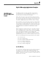
Explicit Messaging Application
Examples
Publication 1769-UM001B-EN-P - October 2002
1756-DNB Explicit Messaging Application Example
Get 1769-ADN Status . . . . . . . . . . . . . . . . . . . .
Get 1769 I/O Module Status . . . . . . . . . . . . . . .
Get 1769 I/O Module Configuration Size. . . . . .
Set 1769 I/O Module Configuration. . . . . . . . . .
Save 1769 I/O Module Configuration . . . . . . . .
Get 1769 I/O Module Configuration . . . . . . . . .
1747-SDN Explicit Messaging Application Example .
Get 1769-ADN Status . . . . . . . . . . . . . . . . . . . .
Get 1769 I/O Module Status . . . . . . . . . . . . . . .
Get 1769 I/O Module Configuration Size. . . . . .
Set 1769 I/O Module Configuration. . . . . . . . . .
Save 1769 I/O Module Configuration . . . . . . . .
Get 1769 I/O Module Configuration . . . . . . . . .
Ladder Logic Example Program . . . . . . . . . . . .
Discrete Module Configuration Files. . . . . . . . . . . .
.
.
.
.
.
.
.
.
.
.
.
.
.
.
.
.
.
.
.
.
.
.
.
.
.
.
.
.
.
.
.
.
v
Appendix C
1769-ADN Throughput
Characteristics
Series A Adapters. . . . . . . . . . . . . . . . . . . . . . . . . . .
About Adapter Throughput Characteristics . . . . . . . . . . .
Turn-Around Time (ttat) . . . . . . . . . . . . . . . . . . . . . . . .
Minimum Inter-Scan Delay (ISD) for Polled Connections
Quick Connect Performance . . . . . . . . . . . . . . . . . . . . .
Quick Connect Limitations . . . . . . . . . . . . . . . . . . . .
.
.
.
.
.
.
.
.
.
.
.
.
C-1
C-1
C-1
C-2
C-3
C-4
Appendix D
Differences Between Series A and About the Differences . . . . . . . . . . . . . . . . . . . . . . . . . . . . D-1
B DeviceNet Adapters
Publication 1769-UM001B-EN-P - October 2002
vi
Notes:
Publication 1769-UM001B-EN-P - October 2002
Preface
Read this preface to familiarize yourself with the rest of the manual.
This preface covers the following topics:
•
•
•
•
•
who should use this manual
how to use this manual
related publications
conventions used in this manual
Allen-Bradley support
Who Should Use This
Manual
Use this manual if you are responsible for designing, installing,
programming, or troubleshooting control systems that use
Allen-Bradley Compact I/O adapters.
How to Use This Manual
As much as possible, we organized this manual to explain, in a
task-by-task manner, how to install, configure, program, operate, and
troubleshoot a control system using the 1769 I/O modules.
Manual Contents
If you want:
1
See:
To install your DeviceNet adapter module
Chapter 1
Information on how communication takes
place and on I/O image table mapping
Chapter 2
To configure your Series A DeviceNet
adapter
Chapter 3
To configure your Series B DeviceNet
adapter
Chapter 4
Information on adapter diagnostics and
troubleshooting
Chapter 5
Information on application examples
Chapter 6
Specifications on the DeviceNet adapter
Appendix A
Information on explicit messaging
application examples
Appendix B
Information on 1769-ADN throughput
characteristics
Appendix C
Information on the differences between
Series A and B DeviceNet adapters
Appendix D
Publication 1769-UM001B-EN-P - October 2002
Preface
2
Related Documentation
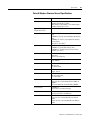
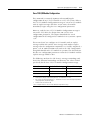
The table below provides a listing of publications that contain
important information about Compact I/O products.
Publication 1769-UM001B-EN-P - October 2002
Title
Publication
Number
MicroLogix 1500 System Overview
1764-SO001
CompactLogix Selection Guide
1769-SG001
Compact I/O Analog Modules User Manual
1769-UM002
1769-ADN Adapter User Manual
1769-UM001
Compact I/O 1769-ADN DeviceNet Adapter Module Installation
Instructions
1769-IN001
Compact 1769-IQ6XOW4 24V dc Sink/Source Input AC/DC Relay
Output Module Installation Instructions
1769-IN002
Compact 1769-OW8 AC/DC Relay Output Module Installation
Instructions
1769-IN003
Compact 1769-OB16P 24V DC Installation Instructions
1769-IN004
Compact 1769-OW8I Individually Isolated AC/DC Relay Output
Module Installation Instructions
1769-IN005
Compact 1769-OW16 16-Point ac/dc Relay Module Installation
Instructions
1769-IN062
Compact 1769-IA16 120V ac Input Module Installation Instructions
1769-IN006
Compact 1769-IQ16 24V dc Sink/Source Input Module Installation
Instructions
1769-IN007
Compact 1769-OB16 Solid State 24V dc Source Output Module
Installation Instructions
1769-IN008
Compact 1769-OA8 100 to 240V ac Solid State Output Module
Installation Instructions
1769-IN009
Compact 1769-OA16 100 to 240V ac Solid State Output Module
Installation Instructions
1769-IN061
Compact 1769-OV16 Solid State 24V dc Sink Output Module
Installation Instructions
1769-IN010
Compact 1769-IM12 240V ac Input Module Installation Instructions
1769-IN011
Compact 1769-IA8I Individually Isolated 120V ac Input Module
Installation Instructions
1769-IN012
Compact 1769-HSC High Speed Counter Module Installation
Instructions
1769-IN030
Compact 1769-HSC High Speed Counter Module User Manual
1769-UM006
Compact 1769-IF4XOF2 Combination Analog Module Installation
Instructions
1769-IN057
Compact 1769-IF4XOF2 Combination Analog User Manual
1769-UM008
Compact 1769 Power Supplies Installation Instructions
1769-5.14
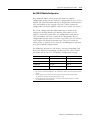
Preface
Title
Publication
Number
Compact I/O Communication Bus Expansion Cables Installation
Instructions
1769-5.15
Compact 1769-ECR Right End Cap/Terminator
1769-5.9
Compact 1769-ECL Left End Cap/Terminator
1769-5.16
Compact 1769-IF4 Analog Input Module Installation Instructions
1769-IN016
Compact 1769-OF2 Analog Output Module Installation Instructions
1769-IN017
3
If you would like a manual, you can:
• download a free electronic version from the internet at
www.theautomationbookstore.com
• purchase a printed manual by:
– contacting your local distributor or Rockwell Automation
representative
– visiting www.theautomationbookstore.com and placing your
order
– calling 1.800.963.9548 (USA/Canada) or
001.330.725.1574 (Outside USA/Canada)
Conventions Used in This
Manual
The following conventions are used throughout this manual:
• Bulleted lists (like this one) provide information, not procedural
steps.
• Numbered lists provide sequential steps or hierarchical
information.
• Italic type is used for emphasis.
• Text in this font indicates words or phrases you should type.
Publication 1769-UM001B-EN-P - October 2002
Preface
4
Allen-Bradley Support
Allen-Bradley offers support services worldwide, with over 75
Sales/Support Offices, 512 authorized distributors and 260 authorized
Systems Integrators located throughout the United States alone, plus
Allen-Bradley representatives in every major country in the world.
Local Product Support
Contact your local Allen-Bradley representative for:
•
•
•
•
sales and order support
product technical training
warranty support
support service agreement
Technical Product Assistance
If you need to contact Allen-Bradley for technical assistance, please
review the information in Chapter 4, Troubleshooting first. Then call
your local Allen-Bradley representative.
Your Questions or Comments on the Manual
If you find a problem with this manual, please notify us using the
self-mailer Publications Problem Report in the back of this manual.
If you have any suggestions for how this manual could be made more
useful to you, please contact us at the address below:
Rockwell Automation
Technical Communication Department
1 Allen-Bradley Drive
Mayfield Heights, OH 44124
Publication 1769-UM001B-EN-P - October 2002
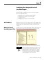
Chapter
1
Installing Your DeviceNet Adapter Module
This chapter explains how to install your DeviceNetTM adapter.
Included is information about:
•
•
•
•
System Assembly
Replacing the 1769-ADN within a System
Field Wiring Connections
Setting the Network Address Switches
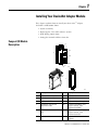
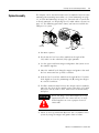
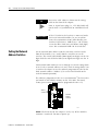
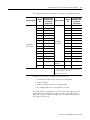
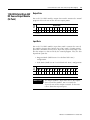
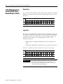
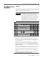
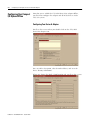
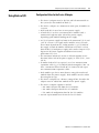
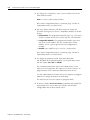
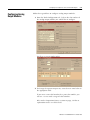
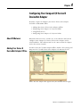
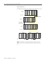
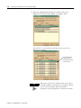
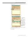
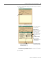
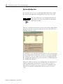
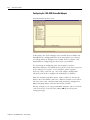
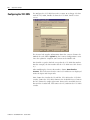
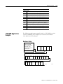
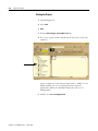
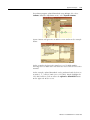
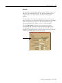
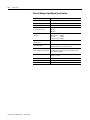
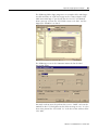
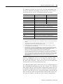
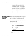
Compact I/O Module
Description
1a
Comm Adapter
2
MS
NS
IO
DIAG
8a
5
8b
3
9
1b
Comm Adapter
6a
MS
NS
IO
DIAG
4
7
6b
1
42125
Item
Description
Item
Description
1a
Upper panel mounting tab
6a
Upper DIN-rail latch
1b
Lower panel mounting tab
6b
Lower DIN-rail latch
2
I/O diagnostic LEDs
7
Write-on label (user I.D. tag)
3
Module door with terminal
identification label
8a
DeviceNet node address rotary
selection switches - Most
Significant Digit (MSD)
4
Stationary bus connector with male 8b
pins
DeviceNet node address rotary
selection switches - Least
Significant Digit (LSD)
5
Nameplate label
Removable DeviceNet terminal
connector
9
Publication 1769-UM001B-EN-P - October 2002
1-2
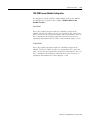
Installing Your DeviceNet Adapter Module
Module Installation
Compact I/O is suitable for use in an industrial environment when
installed in accordance with these instructions. Specifically, this
equipment is intended for use in clean, dry environments (Pollution
degree 21) and circuits not exceeding Over Voltage Category II2 (IEC
60664-1).3
1.
Pollution Degree 2 is an environment where, normally, only non-conductive pollution occurs except that
occasionally a temporary conductivity caused by condensation shall be expected.
2.
Over Voltage Category II is the load level section of the electrical distribution system. At this level transient
voltages are controlled and do not exceed the impulse voltage capability of the product’s insulation.
3.
Pollution Degree 2 and Over Voltage Category II are International Electrotechnical Commission (IEC)
designations.
Prevent Electrostatic Discharge
ATTENTION
!
Electrostatic discharge can damage integrated
circuits or semiconductors if you touch bus
connector pins or the terminal block. Follow these
guidelines when you handle the module:
•
•
•
•
•
•
Touch a grounded object to discharge static potential.
Wear an approved wrist-strap grounding device.
Do not touch the bus connector or connector pins.
Do not touch circuit components inside the module.
If available, use a static-safe work station.
When not in use, keep the module in its static-shield box.
Remove Power
ATTENTION
!
Remove power before removing or inserting this
adapter. When you remove or insert an adapter
with power applied, an electrical arc may occur.
An electrical arc can cause personal injury or
property damage by:
• sending an erroneous signal to your system’s field devices,
causing unintended machine motion
• causing an explosion in a hazardous environment
Electrical arcing causes excessive wear to contacts
on both the module and its mating connector.
Worn contacts may create electrical resistance.
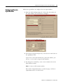
System Configuration
Publication 1769-UM001B-EN-P - October 2002
Refer to Using Banks of I/O on page 3-7 for system configuration
rules.
Installing Your DeviceNet Adapter Module
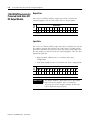
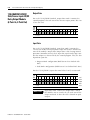
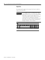
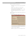
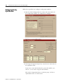
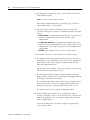
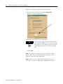
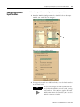
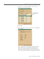
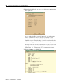
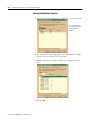
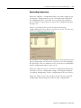
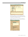
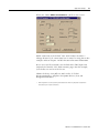
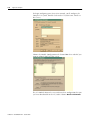
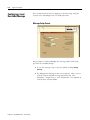
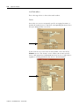
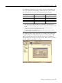
System Assembly
1-3
The adapter can be attached to adjacent 1769 modules before or after
mounting. For mounting instructions, see “Panel Mounting” on page
1-4, or “DIN Rail Mounting” on page 1-6. To work with a system that
is already mounted, see “Replacing the 1769-ADN within a System” on
page 1-6. The following procedure shows you how to assemble the
Compact I/O system.
a
b
c
a
e
1769-ADN
a
a
d
42126
1. Disconnect power.
2. Check that the bus lever of the module to the right of the
1769-ADN is in the unlocked (fully right) position.
3. Use the upper and lower tongue-and-groove slots (a) to secure
the modules together.
4. Move the module back along the tongue-and-groove slots until
the bus connectors line up with each other.
5. Push the bus lever of the module to the right of the 1769-ADN
back slightly to clear the positioning tab (b) using your fingers
or a small screwdriver.
6. To allow communication between the adapter and I/O modules,
move the bus lever of the module to the right of the 1769-ADN
fully to the left (c) until it clicks. Make sure it is locked firmly
into place.
ATTENTION
!
When attaching a 1769-ADN adapter, it is very
important that the bus connectors are securely
locked together to create a proper electrical
connection.
7. Attach an end cap terminator (d) to the last I/O module in the
system by using the tongue-and-groove slots as before.
Publication 1769-UM001B-EN-P - October 2002
1-4
Installing Your DeviceNet Adapter Module
8. Lock the end cap bus terminator (e).
A 1769-ECR or 1769-ECL right or left end cap
must be used to terminate the end of the serial
communication bus.
IMPORTANT
9. Refer to the “DeviceNet Wiring” section on page 1-7.
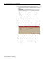
Mounting the Adapter and
an I/O Module
ATTENTION
!
During panel or DIN rail mounting of all devices,
be sure that all debris (metal chips, wire strands,
etc.) is kept from falling into the adapter or
modules. Debris that falls into the adapter or
modules could cause damage on power up.
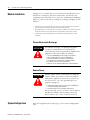
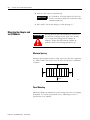
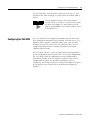
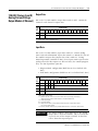
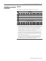
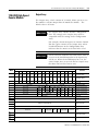
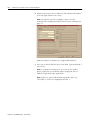
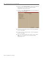
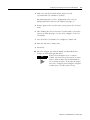
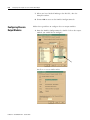
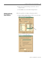
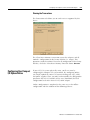
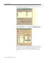
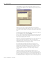
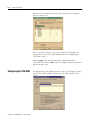
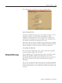
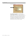
Minimum Spacing
Maintain spacing from enclosure walls, wireways, adjacent equipment,
etc. Allow 50mm (2in) of space on all sides for adequate ventilation,
as shown:
End Cap or Cable
1769 I/O
1769 I/O
1769 I/O
1769 I/O
1769 Power Supply
1769 I/O
1769 I/O
Side
1769-ADN
Top
Side
Bottom
42124
Panel Mounting
Mount the adapter or module to a panel using two screws per adapter
or module. Use M4 or #8 panhead screws. Mounting screws are
required on every module.
Publication 1769-UM001B-EN-P - October 2002
Installing Your DeviceNet Adapter Module
1-5
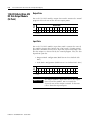
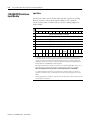
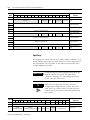
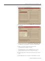
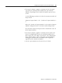
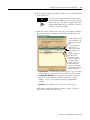
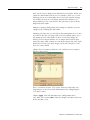
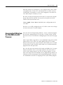
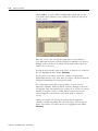
Panel Mounting Using the Dimensional Template
For more than 1 module: Number of modules x 35mm (1.38in)
35
35
Right End Cap
1769 I/O
28.5
(1.12)
1769 I/O
35
(1.38)
1769 Power Supply
122.6+0.2
(4.826+0.008)
70
(2.76)
1769-ADN
132
(5.197)
40
(1.58)
Hole spacing tolerance:
+0.4mm (0.016in).
mm (in)
(1.38) (1.38)
42121
Panel Mounting Procedure Using Modules as a Template
The following procedure allows you to use the assembled adapter and
modules as a template for drilling holes in the panel. If you have
sophisticated panel mounting equipment, you can use the
dimensional template provided on page 1-5.
Due to the module mounting hole tolerance, it is important to follow
these procedures:
1. On a clean work surface, assemble no more than three modules.
2. Using the assembled modules as a template, carefully mark the
center of all module-mounting holes on the panel.
3. Return the assembled modules to the clean work surface,
including any previously mounted modules.
4. Drill and tap the mounting holes for the recommended M4 or
#8 screw.
5. Place the modules back on the panel and check for proper hole
alignment.
6. Attach the modules to the panel using the mounting screws.
NOTE: If mounting more modules, mount only the last one of
this group and put the others aside. This reduces remounting
time during drilling and tapping of the next group.
7. Repeat steps 1 through 6 for any remaining modules.
Publication 1769-UM001B-EN-P - October 2002
1-6
Installing Your DeviceNet Adapter Module
DIN Rail Mounting
The adapter can be mounted using the following DIN rails:
• 35 x 7.5mm (EN50022 - 35 x 7.5)
• 35 x 15mm (EN 50022 - 35 x 15)
Before mounting the module on a DIN rail, close the DIN rail latches.
Press the DIN rail mounting area of the module against the DIN rail.
The latches will momentarily open and lock into place.
Replacing the 1769-ADN
within a System
The adapter can be replaced while the system is mounted to a panel
(or DIN rail).
1. Remove power. See important note on page 1-2.
2. Remove the DeviceNet cable from the module by loosening the
upper and lower retaining screws of the DeviceNet connector
and removing the connector from the module.
3. Remove the upper and lower mounting screws from the adapter
(or open the DIN latches using a flat-blade or phillips-style
screwdriver).
4. On the right-side adjacent module, move its bus lever to the
right (unlock) to disconnect it from the adapter being removed.
5. Gently slide the disconnected adapter forward.
If you feel excessive resistance, make sure that you
disconnected the adapter from the bus and that you removed
both mounting screws (or opened the DIN latches).
Note: It may be necessary to rock the module slightly from front
to back to remove it, or, in a panel-mounted system, to loosen
the screws of adjacent modules.
6. Before installing the replacement adapter, be sure that the bus
lever on the right-side adjacent module is in the unlocked (fully
right) position.
7. Slide the replacement adapter into the open slot.
8. Connect the adapter and modules together by locking (fully left)
the bus lever on the right-side adjacent module.
9. Replace the mounting screws (or snap the adapter onto the DIN
rail).
Publication 1769-UM001B-EN-P - October 2002
Installing Your DeviceNet Adapter Module
1-7
10. Replace the DeviceNet cable on the module by tightening the
upper and lower retaining screws and attaching the connector to
the module.
Set the network address switches to the same value as the removed
adapter.
Grounding the Adapter
This product is intended to be mounted to a well-grounded mounting
surface such as a metal panel. Additional grounding connections from
the adapter’s mounting tabs or metal DIN rail (if used), are not
required unless you cannot ground the mounting surface. Refer to
Industrial Automation Wiring and Grounding Guidelines, publication
1770-4.1, for additional information.
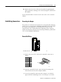
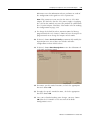
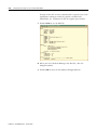
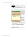
DeviceNet Wiring
Comm Adapter
Field Wiring Connections
MS
NS
IO
DIAG
DeviceNet Connector
42123
1. Connect the DeviceNet cable to the removable connector as
shown.
Connect
To
BLK Wire
-V
BLU Wire
CAN Low
Bare Wire
Drain
WHT Wire
CAN High
RED Wire
+V
BLK
BLU
Bare
WHT RED
Connector
42122
2. Insert the removable female connector into the mating male
connector on the DeviceNet adapter module.
3. Screw the removable connector to the adapter case with the
upper and lower mounting screws. Screw torque is 5-6 in-lbs.
Publication 1769-UM001B-EN-P - October 2002
1-8
Installing Your DeviceNet Adapter Module
TIP
DeviceNet cable colors are shown on the wiring
label on the front of the adapter.
Note: A 10-pin linear plug (i.e., 1787-PLUG10R) will
not fit while a 1799-DNETCON or -DNETSCON will
fit.
IMPORTANT
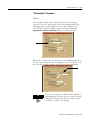
Setting the Network
Address Switches
If the 1769-ADN is the last device connected to the
DeviceNet network trunkline, be sure to add or
move the termination resistor (Allen-Bradley part
number 1485A-C2 or a 120Ω 5% or > ¼W resistor)
across the Blue (CAN Low) and White (CAN High)
wires. We recommend 121Ω ¼W 1% metal film.
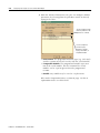
Set the network node address with the two rotary switches on the
front of the module. Use a small, slotted screwdriver to set the
switches. The switch labeled MSD (Most Significant Digit) sets the 10s
digit while the switch labeled LSD (Least Significant Digit) sets the 1s
digit.
Valid network node addresses are 00 through 63. Switch settings from
00 to 63 select network addresses 00 to 63. Switch settings from 64 to
99 instruct the adapter to use the software programmed value for the
node network address. (Address 95 is reserved and should not be
used for normal operation.)
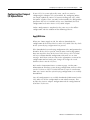
Comm Adapter
The software programmed value is set via RSNetworxTM for DeviceNet
and stored in non-volatile memory on the 1769-ADN. The initial,
factory-preset setting of the software programmed value is 63.
MS
NS
IO
DIAG
Address
Switches
Network
Address
Switches
42127
NOTE: The baud rate for the adapter is set by way of the module’s
automatic “auto baud” function at power-up.
Publication 1769-UM001B-EN-P - October 2002
Installing Your DeviceNet Adapter Module
1-9
Use the removable, write-on label to mark your I.D. tag, etc. with
permanent ink. Your markings are visible when the module door is
closed.
TIP
Configuring the 1769-ADN
Series B adapters that have their node address
switches set to 95, startup in a special factory mode
that does not support I/O connections. Series B
adapters should not have their node address set to
95 for normal use.
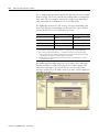
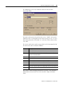
The 1769-ADN must be configured with RSNetworx for DeviceNet.
This configuration tool allows you to identify all of the devices (I/O
modules, power supplies, expansion cables, end caps) and their
locations in your 1769 system. The 1769-ADN must have the I/O
configuration loaded into its’ memory to perform the network
communication function.
The 1769-ADN will not accept I/O connections if the programmed
system configuration does not match the actual system configuration.
The 1769-ADN retains the programmed system configuration in
non-volatile memory so it can compare it with the actual system
configuration on power-up. For more information, refer to
Configuring Your Compact I/O Series A DeviceNet Adapter in Chapter 3
or Configuring Your Compact I/O Series B DeviceNet Adapter in
Chapter 4.
Publication 1769-UM001B-EN-P - October 2002
1-10
Installing Your DeviceNet Adapter Module
Notes:
Publication 1769-UM001B-EN-P - October 2002
Chapter
2
How Communication Takes Place and I/O
Image Table Mapping
This chapter explains how communication takes place and about I/O
image table mapping. Included is information about:
• I/O Structure
• Communication Choices
• Mapping I/O Data into the Image Table
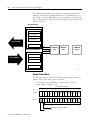
Communication Over the
1769 Bus
One 1769-ADN DeviceNet adapter can interface with up to 30
Compact I/O modules to make a Compact I/O system. The adapter
communicates to other network system components (typically a
controller or scanner and/or programming terminals) over the
DeviceNet network.
The adapter communicates with its I/O modules over the 1769 bus.
The adapter and I/O modules also receive 5Vdc and 24V dc power
through the bus interface via a 1769 power supply. The 1769 bus and
all devices on the 1769 bus have system configuration limits. Refer to
Using Banks of I/O on page 3-7 for more information.
The I/O map for an I/O module is divided into input data words and
output data words. The number of input data words or output data
words can be 0 or more. The length of each I/O module’s input data
words or output data words vary in size, depending on the module’s
complexity. Each I/O module will support at least one input data
word or one output data word.
I/O Structure
Output data is received by the adapter in the order of the installed I/O
modules. The output data for Slot 1 is received first, followed by the
output data for Slot 2, and so on up to Slot 30.
The amount of output data in the adapter’s output image for each I/O
module is based on the configuration of each I/O module done as
part of the 1769-ADN configuration. If an I/O module is configured to
have 0 words of output data, then it does not appear in the output
image of the 1769-ADN. Only a module’s output data can be in the
1769-ADN output image - a module’s configuration data cannot.
The first two words of input data sent by the adapter are the Adapter
Status Words. This is followed by the input data from each slot, in the
order of the installed I/O modules. The input data from Slot 1 is first
after the status words, followed by Input data from Slot 2, and so on
up to Slot 30.
1
Publication 1769-UM001B-EN-P - October 2002
2-2
How Communication Takes Place and I/O Image Table Mapping
The amount of input data in the adapter’s input image for each I/O
module is based on the configuration of each I/O module done as
part of the 1769-ADN configuration. If an I/O module is configured to
have 0 words of input data, then it does not appear in the input image
of the 1769-ADN.
DeviceNet Adapter
Input Image (Read Data)
Adapter Status Words
Slot 1 Input Data
Slot 2 Input Data
Slot 3 Input Data
...
Network READ
Slot 30 Input Data
Read
Output Image (Write Data)
I/O Module
Slot 1
...
I/O Module
Slot 2
I/O Module
Slot 30
Write
Slot 1 Output Data
Network WRITE
Slot 2 Output Data
Slot 3 Output Data
...
Slot 30 Output Data
42279
Adapter Status Words
The first two words (0 and 1) of the adapter input image contain the
adapter status. The adapter status consists of:
• I/O module data invalid bits - 1 status bit for each slot
• node address changed - 1 bit
I/O Module Data Invalid Bits
Slot 2
Slot 1
20
19
18
17
16
Slot 21
Slot 20
Slot 19
Slot 18
Slot 17
Slot 3
21
Slot 4
22
Slot 5
Slot 6
23
Slot 22
0
24
Node Address Changed Bit (NACB)
Publication 1769-UM001B-EN-P - October 2002
1
25
I/O Module Data Invalid Bits
Spare, not used
2
Slot 7
Slot 26
3
Slot 23
Slot 27
4
Slot 8
26
5
Slot 24
27
6
Slot 9
28
7
Slot 25
Slot 11
29
8
Slot 10
Slot 12
30
Slot 28
9
Slot 13
10
Slot 29
11
Slot 14
12
Slot 30
13
Slot 15
Word 1
14
NACB
Word 0
15
Slot 16
Bit:
42280
How Communication Takes Place and I/O Image Table Mapping
2-3
The adapter status bit descriptions are shown in the following table.
Bit Description
I/O Module
Data Invalid
Word 0
Bit
Is set (1) when
I/O module data
is invalid for
slot position
Word 1
Bit
Is set (1) when
I/O module data
is invalid for
slot position
0
1
0
17
1
2
1
18
2
3
2
19
3
4
3
20
4
5
4
21
5
6
5
22
6
7
6
23
7
8
7
24
8
9
8
25
9
10
9
26
10
11
10
27
11
12
11
28
12
13
12
29
13
14
13
30
14
15
Node Address
Changed
14
1
-
15
16
Not Used
152
-
Bit Description
I/O Module
Data Invalid
1
This bit is set (1) when the node address switch setting
has been changed since powerup.
2
Not used - sent as zeroes.
Possible causes for an I/O Module Data Invalid are:
•
•
•
•
transmission errors on the Compact I/O backplane
a failed module
incorrect module inserted in a slot position
the configuration for an I/O module is invalid
The node address changed bit is set when the node address switch
setting has been changed since power up. The new node address
does not take affect until the adapter has been powered down and
then powered back up.
Publication 1769-UM001B-EN-P - October 2002
2-4
How Communication Takes Place and I/O Image Table Mapping
Communication Choices
The Compact I/O DeviceNet adapter module supports multiple
communication choices. These choices all use the DeviceNet adapter
input image and output image structure previously described. The
DeviceNet master makes the actual communication choice. The
choices are:
Polled1 - data is sent by the adapter in response to received data
Strobe - data is sent by the adapter in response to the strobe
command. The single bit allocated to the adapter in the strobe
message is not used. If the configured size of the input image (sent
from the adapter) is greater than 8 bytes, only the first 8 bytes of the
input image are returned (of which, the first 4 bytes, or 2 words, are
the adapter status words).
Change of State - data is sent by the adapter based on detection of
any changed value within the input data. Data is independently
received based on change of state from the sender. Data in both
directions can be acknowledged or unacknowledged depending on
the run time configuration of the system.
Cyclic - data is sent cyclically by the adapter based on a configured
time value. Data is independently received cyclically from the sender.
Data in both directions can be acknowledged or unacknowledged
depending on the run time configuration of the system.
1
Mapping I/O Data into the
Image Table
Refer to Appendix C for some important system characteristics when using the polled mode (minimum
inter-scan delay I.D. for polled connections).
All Compact I/O modules are supported by the Series B DeviceNet
adapter. At present, these consist of:
Module Description
For I/O data
definition, see:
1769-IA8I Individually Isolated 120V AC Input Module (8 Point)
2-5
1769-IA16 120V ac Input Module (16 Point) (16 Point)
2-5
1769-IF4 (Series A and B) Analog Current/Voltage Input Module (4 Channel)
2-6
1769-IM12 240V AC Input Module (12 Point)
2-6
1769-IQ16 24V DC Sink/Source Input Module (16 Point)
2-6
1769-OA8 100 to 240V AC Solid State Output Module (8 Point)
2-7
1769-OA16 100 to 240V AC Solid State Output Module (16 Point)
2-8
1769-OB16 Solid State 24V DC Source Output Module (16 Point)
2-9
1769-OB16P Electronically Protected Solid-State 24V DC Output Module
2-10
1769-OF2 (Series A and B) Analog Current/Voltage Output Module (2 Channel)
2-11
1769-OV16 Solid State 24V DC Sink Output Module (16 Point)
2-12
Publication 1769-UM001B-EN-P - October 2002
How Communication Takes Place and I/O Image Table Mapping
Module Description
For I/O data
definition, see:
1769-OW8 AC/DC Relay Output Module (8 Point)
2-13
1769-OW8I Individually Isolated AC/DC Relay Output Module (8 Point)
2-14
1769-OW16 AC/DC Relay Output Module (16 Point)
2-15
1769-IQ6XOW4 24V DC Sink/Source Input AC/DC Relay Output Module (6 Point In, 4 Point Out)
2-16
1769-IT6 Thermocouple/mV Input Module
2-17
1769-IR6 RTD/Resistance Input Module
2-18
1769-IF4XOF2 Combination Analog Module
2-19
1769-HSC High-Speed Counter Module
2-21
IMPORTANT
2-5
These modules will only operate properly with
Series B DeviceNet adapters: 1769-OW16, -OA16,
-IF4XOF2, -HSC.
The following sections, as referenced above, give the input and
output data definitions for each Compact I/O module type. Their
mapping into the adapter’s input and output images are dependent on
their slot number and configured input and output sizes (as defined in
the I/O Structure section on page 2-1).
Input Data
For each 1769-IA8I input module, input data word 0 contains the
current state of the field input points. Bits 8 to 15 are not used.
Word
1769-IA8I Individually
Isolated 120V AC Input
Module (8 Point)
0
Bit Position
15 14 13 12 11 10
9
8
7
6
5
4
3
2
1
0
0
0
0
r
r
r
r
r
r
r
r
0
0
0
0
0
r = read
Input Data
For each 1769-IA16 input module, input data word 0 contains the
current state of the field input points.
Word
1769-IA16 120V ac Input
Module (16 Point)
0
Bit Position
15 14 13 12 11 10
r
r
r
r
r
r
9
8
7
6
5
4
3
2
1
0
r
r
r
r
r
r
r
r
r
r
r = read
Publication 1769-UM001B-EN-P - October 2002
How Communication Takes Place and I/O Image Table Mapping
1769-IF4 (Series A and B)
Analog Current/Voltage
Input Module (4 Channel)
Input Data
For each 1769-IF4 input module, input data words 0-3 contain the
analog value of the inputs. Word 4 and 5 contain analog status and
error information.
Bit Position
Word
2-6
15
0
SGN
Analog Input Data Channel 0
1
SGN
Analog Input Data Channel 1
2
SGN
Analog Input Data Channel 2
3
SGN
Analog Input Data Channel 3
14 13 12 11 10
4
9
8
7
6
5
4
Not Used
5
U0
3
2
1
0
S3 S2 S1 S0
O0 U1 O1 U2 O2 U3 O3
Set to 0
SGN= sign bit in two’s format
Sx = general status bit for channels 0 through 3. This bit is set (1) when an error (over- or
under-range) exists for that channel.
Ux = under-range flag bits for channels 0 through 3. These bits can be used in the control
program for error detection.
Ox = over-range flag bits for channels 0 through 3. These bits can be used in the control
program for error detection.
1769-IM12 240V AC Input
Module (12 Point)
Input Data
Word
For each 1769-IM12 input module, input data word 0 contains the
current state of the field input points. Bits 12 to 15 are not used.
0
Bit Position
15 14 13 12 11 10
9
8
7
6
5
4
3
2
1
0
0
r
r
r
r
r
r
r
r
r
r
0
0
0
r
r
r = read
Input Data
For each 1769-IQ16 input module, input data word 0 contains the
current state of the field input points.
Word
1769-IQ16 24V DC
Sink/Source Input Module
(16 Point)
0
Bit Position
15 14 13 12 11 10
r
r = read
Publication 1769-UM001B-EN-P - October 2002
r
r
r
r
r
9
8
7
6
5
4
3
2
1
0
r
r
r
r
r
r
r
r
r
r
How Communication Takes Place and I/O Image Table Mapping
Output Data
Word
For each 1769-OA8 module, output data word 0 contains the control
program’s directed state of the discrete output points. Bits 8 to 15 are
not used.
0
Bit Position
15 14 13 12 11 10
9
8
7
6
5
4
3
2
1
0
0
0
0
w
w
w
w
w
w
w
w
0
0
0
0
0
w = write
Input Data
For each 1769-OA8 module, input data word 0 contains the state of
the module’s output data (output data echo) word 0. During normal
operation (controller in Run), these input bits represent the logic state
that the outputs are directed to by the control program. They are also
dependent upon the:
• Program Mode (Hold Last or User-Defined Safe State)
configuration
• Fault Mode (Hold Last or User-Defined Safe State) configuration
For the 1769-OA8, input data word 0 bits 8 to 15 are not used.
Word
1769-OA8 100 to 240V AC
Solid State Output Module
(8 Point)
2-7
0
Bit Position
15 14 13 12 11 10
9
8
7
6
5
4
3
2
1
0
0
0
0
r
r
r
r
r
r
r
r
0
0
0
0
0
r = read
IMPORTANT
The output module’s input data reflects the output
data echo of the module, not necessarily the
electrical state of the output terminals. It does not
reflect shorted or open outputs.
Publication 1769-UM001B-EN-P - October 2002
2-8
How Communication Takes Place and I/O Image Table Mapping
1769-OA16 100 to 240V AC
Solid State Output Module
(16 Point)
Output Data File
Data output bits are turned on or off using the bit positions in Word 0.
1 = output on
0 = output off
Example: To turn on bit position 12, type 1 in Word 0, Bit 12.
For each module, slot x, word 0 in the output data file contains the
control program’s directed state of the discrete output points.
Word
Bit Position
15
14
13
12
11
10
9
8
7
6
5
4
3
2
1
0
0
w
w
w
w
w
w
w
w
w
w
w
w
w
w
w
w
w = write
Output Module’s Input Data File
For each module, slot x, input data file word 0 contains the state of
the module’s output data (output data echo) file word 0. During
normal operation, these input bits represent the logic state that the
outputs are directed to by the control program. They are also
dependent upon the:
• Program Mode configuration (if supported by the controller)
• The Fault Mode configuration (if supported by the controller)
Word
Bit Position
15
14
13
12
11
10
9
8
7
6
5
4
3
2
1
0
0
r
r
r
r
r
r
r
r
r
r
r
r
r
r
r
r
r = read
IMPORTANT
The output module’s input data file reflects the
output data echo of the module, not necessarily the
electrical state of the output terminals. It does not
reflect shorted or open outputs.
It is important to use this input word if the controller
adapter supports the Program Mode or Fault Mode
function, and if it is configured to use them.
Publication 1769-UM001B-EN-P - October 2002
How Communication Takes Place and I/O Image Table Mapping
Output Data
Word
For each 1769-OB16 module, output data word 0 contains the control
program’s directed state of the discrete output points.
0
Bit Position
15 14 13 12 11 10
9
8
7
6
5
4
3
2
1
0
w
w
w
w
w
w
w
w
w
w
w
w
w
w
w
w
w = write
Input Data
For each 1769-OB16 module, input data word 0 contains the state of
the module’s output data (output data echo) word 0. During normal
operation (controller in Run), these input bits represent the logic state
that the outputs are directed to by the control program. They are also
dependent upon the:
• Program Mode (Hold Last or User-Defined Safe State)
configuration
• Fault Mode (Hold Last or User-Defined Safe State) configuration
Word
1769-OB16 Solid State 24V
DC Source Output Module
(16 Point)
2-9
0
Bit Position
15 14 13 12 11 10
r
r
r
r
r
r
9
8
7
6
5
4
3
2
1
0
r
r
r
r
r
r
r
r
r
r
r = read
IMPORTANT
The output module’s input data reflects the output
data echo of the module, not necessarily the
electrical state of the output terminals. It does not
reflect shorted or open outputs.
Publication 1769-UM001B-EN-P - October 2002
2-10
How Communication Takes Place and I/O Image Table Mapping
Output Data
For each 1769-OB16P module, output data word 0 contains the
control program’s directed state of the discrete output points.
Word
1769-OB16P Electronically
Protected Solid-State 24V
DC Output Module
0
Bit Position
15 14 13 12 11 10
9
8
7
6
5
4
3
2
1
0
w
w
w
w
w
w
w
w
w
w
w
w
w
w
w
w
w = write
Input Data
For each 1769-OB16P module, input data word 0 contains the state of
the module’s output data (output data echo) word 0. During normal
operation (controller in Run), these input bits represent the logic state
that the outputs are directed to by the control program. They are also
dependent upon the:
• Program Mode (Hold Last or User-Defined Safe State)
configuration
Word
• Fault Mode (Hold Last or User-Defined Safe State) configuration
0
Bit Position
15 14 13 12 11 10
r
r
r
r
r
r
9
8
7
6
5
4
3
2
1
0
r
r
r
r
r
r
r
r
r
r
r = read
IMPORTANT
Publication 1769-UM001B-EN-P - October 2002
The output module’s input data reflects the output
data echo of the module, not necessarily the
electrical state of the output terminals. It does not
reflect shorted or open outputs.
How Communication Takes Place and I/O Image Table Mapping
2-11
1769-OF2 (Series A and B) Output Data
Analog Current/Voltage
Output Module (2 Channel) For each 1769-OF2 module, output data words 0 and 1 contain the
channel 0 and channel 1 output data.
Word
Bit Position
15
0
SGN
Analog Output Data Channel 0
1
SGN
Analog Output Data Channel 1
14 13 12 11 10
9
8
7
6
5
4
3
2
1
0
SGN= sign bit in two’s compliment format
Input Data
For each 1769-OF2 module, input data words 0-1 contain analog
status and error information. Input data words 2-3 contain the state of
the module’s output data (output data echo) words 0-1. During
normal operation (controller in Run), these input words represent the
analog values that the outputs are directed to by the control program.
They are also dependent upon the:
• Program Mode configuration (Hold Last or User-Defined Safe
State)
• Fault Mode configuration (Hold Last or User-Defined Safe State)
Word
Bit Position
15
14 13 12 11 10
0
D0
H0 D1 H1
Not Used (Bits set to 0)
1
U0
O0 U1 O1
Bits set to 0
2
SGN
Output Data Loopback/Echo Channel 0
3
SGN
Output Data Loopback/Echo Channel 1
9
8
7
6
5
4
3
2
1
0
S1 S0
SGN= sign bit in two’s format
Sx = general status bits. When set, these bits indicate an error (over-range, under-range, or
diagnostic bit) associated with that channel or a module hardware error.
Ux = under-range flag bits
Ox = over-range flag bits
Dx = diagnostic bits. When set, they indicate a broken output wire or high load resistance
(not used on voltage outputs).
Hx = hold last state bits. When set, they indicate that the channel is in a hold last state condition.
IMPORTANT
The output module’s input data reflects the analog
output data echo of the module, not necessarily the
electrical state of the output terminals. It does not
reflect shorted or open outputs.
Publication 1769-UM001B-EN-P - October 2002
2-12
How Communication Takes Place and I/O Image Table Mapping
Output Data
For each 1769-OV16 module, output data word 0 contains the control
program’s directed state of the discrete output points.
Word
1769-OV16 Solid State 24V
DC Sink Output Module
(16 Point)
0
Bit Position
15 14 13 12 11 10
9
8
7
6
5
4
3
2
1
0
w
w
w
w
w
w
w
w
w
w
w
w
w
w
w
w
w = write
Input Data
For each 1769-OV16 module, input data word 0 contains the state of
the module’s output data (output data echo) word 0. During normal
operation (controller in Run), these input bits represent the logic state
that the outputs are directed to by the control program. They are also
dependent upon the:
Word
• Program Mode configuration (Hold Last or User-Defined Safe
State)
• Fault Mode configuration (Hold Last or User-Defined Safe State)
0
Bit Position
15 14 13 12 11 10
r
r
r
r
r
r
9
8
7
6
5
4
3
2
1
0
r
r
r
r
r
r
r
r
r
r
r = read
IMPORTANT
Publication 1769-UM001B-EN-P - October 2002
The output module’s input data reflects the output
data echo of the module, not necessarily the
electrical state of the output terminals. It does not
reflect shorted or open outputs.
How Communication Takes Place and I/O Image Table Mapping
Output Data
Word
For each 1769-OW8 module, output data word 0 contains the control
program’s directed state of the discrete output points. Bits 8 to 15 are
not used.
0
Bit Position
15 14 13 12 11 10
9
8
7
6
5
4
3
2
1
0
0
0
0
w
w
w
w
w
w
w
w
0
0
0
0
0
w = write
Input Data
For each 1769-OW8 module, input data word 0 contains the state of
the module’s output data (output data echo). During normal operation
(controller in Run), these input bits represent the logic state that the
outputs are directed to by the control program. They are also
dependent upon the:
• Program Mode configuration (Hold Last or User-Defined Safe
State)
• Fault Mode configuration (Hold Last or User-Defined Safe State)
For the 1769-OW8, input data word 0 bits 8 to 15 are not used.
Word
1769-OW8 AC/DC Relay
Output Module (8 Point)
2-13
0
Bit Position
15 14 13 12 11 10
9
8
7
6
5
4
3
2
1
0
0
0
0
r
r
r
r
r
r
r
r
0
0
0
0
0
r = read
IMPORTANT
The output module’s input data reflects the output
data echo of the module, not necessarily the
electrical state of the output terminals. It does not
reflect shorted or open outputs.
Publication 1769-UM001B-EN-P - October 2002
2-14
How Communication Takes Place and I/O Image Table Mapping
Output Data
For each 1769-OW8I module, output data word 0 contains the control
program’s directed state of the discrete output points. Bits 8 to 15 are
not used.
Word
1769-OW8I Individually
Isolated AC/DC Relay
Output Module (8 Point)
0
Bit Position
15 14 13 12 11 10
9
8
7
6
5
4
3
2
1
0
0
0
0
w
w
w
w
w
w
w
w
0
0
0
0
0
w = write
Input Data
For each 1769-OW8I module, input data word 0 contains the state of
the module’s output data (output data echo). During normal operation
(controller in Run), these input bits represent the logic state that the
outputs are directed to by the control program. They are also
dependent upon the:
• Program Mode configuration (Hold Last or User-Defined Safe
State)
• Fault Mode configuration (Hold Last or User-Defined Safe State)
Word
For the 1769-OW8I, input data word 0 bits 8 to 15 are not used.
0
Bit Position
15 14 13 12 11 10
9
8
7
6
5
4
3
2
1
0
0
0
0
r
r
r
r
r
r
r
r
0
0
0
0
0
r = read
IMPORTANT
Publication 1769-UM001B-EN-P - October 2002
The output module’s input data reflects the output
data echo of the module, not necessarily the
electrical state of the output terminals. It does not
reflect shorted or open outputs.
How Communication Takes Place and I/O Image Table Mapping
Output Data File
Data output bits are turned on or off using the bit positions in Word 0.
1 = output on
0 = output off
Example: To turn on bit position 12, type 1 in Word 0, Bit 12.
For each module, slot x, word 0 in the output data file contains the
control program’s directed state of the discrete output points.
Word
Bit Position
15
14
13
12
11
10
9
8
7
6
5
4
3
2
1
0
0
w
w
w
w
w
w
w
w
w
w
w
w
w
w
w
w
w = write only
Output Module’s Input Data File
For each module, slot x, input data file word 0 contains the state of
the module’s output data (output data echo) file word 0. During
normal operation, these input bits represent the logic state that the
outputs are directed to by the control program. They are also
dependent upon the:
• Program Mode configuration (if supported by the controller)
• The Fault Mode configuration (if supported by the controller).
Bit Position
Word
1769-OW16 AC/DC Relay
Output Module (16 Point)
2-15
15
14
13
12
11
10
9
8
7
6
5
4
3
2
1
0
0
r
r
r
r
r
r
r
r
r
r
r
r
r
r
r
r
r = read only
IMPORTANT
The output module’s input data file reflects the
output data echo of the module, not necessarily the
electrical state of the output terminals. It does not
reflect shorted or open outputs.
It is important to use this input word if the controller
adapter supports the Program Mode or Fault Mode
function, and if it is configured to use them.
Publication 1769-UM001B-EN-P - October 2002
2-16
How Communication Takes Place and I/O Image Table Mapping
Output Data
For each 1769-IQ6XOW4 module, output data word 0 contains the
control program’s directed state of the discrete output points. Bits 4 to
15 are not used.
Word
1769-IQ6XOW4 24V DC
Sink/Source Input AC/DC
Relay Output Module
(6 Point In, 4 Point Out)
0
Bit Position
15 14 13 12 11 10
9
8
7
6
5
4
3
2
1
0
0
0
0
0
0
0
0
w
w
w
w
0
0
0
0
0
w = write
Input Data
For each 1769-IQ6XOW4 module, input data word 0 contains the
current state of the field input points. Input data word 1 contains the
state of the module’s output data (output data echo). During normal
operation (controller in Run), these input bits represent the logic state
that the outputs are directed to by the control program. They are also
dependent upon the:
• Program Mode configuration (Hold Last or User-Defined Safe
State)
• Fault Mode configuration (Hold Last or User-Defined Safe State)
Word
For the 1769-IQ6XOW4, input data word 0 bits 6 to 15 are not used.
Bit Position
15 14 13 12 11 10
9
8
7
6
5
4
3
2
1
0
0
0
0
0
0
0
0
0
0
0
0
r
r
r
r
r
r
1
0
0
0
0
0
0
0
0
0
0
0
0
r
r
r
r
r = read
IMPORTANT
Publication 1769-UM001B-EN-P - October 2002
real
inputs
output
data
echo
Input data word 1 reflects the output data echo of
the module, not necessarily the electrical state of the
output terminals. It does not reflect shorted or open
outputs.
How Communication Takes Place and I/O Image Table Mapping
2-17
1769-IT6 Thermocouple/mV Input Data
Input Module
Word
The input data file contains the analog values of the inputs.
Bit Position
15
14
13
12
11
10
9
8
7
6
0
Analog Input Data Channel 0
1
Analog Input Data Channel 1
2
Analog Input Data Channel 2
3
Analog Input Data Channel 3
4
Analog Input Data Channel 4
5
Analog Input Data Channel 5
5
4
3
2
1
0
6 OC7 OC6 OC5 OC4 OC3 OC2 OC1 OC0 S7 S6 S5 S4 S3 S2 S1 S0
7
U0
O0
U1
U0
U2
O2
U3
O3
U4 O4 U5 O5 U6 O6 U7 O7
Sx = General status bit for channels 0-5 and CJC sensors (S6 and S7). This bit is set (1) when an error
(over-range, under-range, open-circuit, or input data not valid) exists for that channel. An input data not valid
condition is determined by the user program. This condition occurs when the first analog-to-digital conversion
is still in progress, after a new configuration has been sent to the module. Refer to the Compact™ I/O
Thermocouple/mV Input Module User Manual, publication 1769-UM004A-EN-P for additional details.
OCx = Open circuit detection bits indicate an open input circuit on channels 0-5 (OC0 - OC5) and on CJC sensors
CJC0 (OC6) and CJC1 (OC7). The bit is set (1) when an open-circuit condition exists.
Ux = Under-range flag bits for channels 0-5 and the CJC sensors (U6 and U7). For thermocouple inputs, the
under-range bit is set (1) when a temperature measurement is below the normal operating range for a given
thermocouple type. For millivolt inputs, the under-range bit indicates a voltage that is below the normal
operating range. These bits can be used in the control program for error detection. The bits are reset (0) by the
module when within the normal operating range.
Ox = Over-range flag bits for channels 0-5 and the CJC sensors (O6 and O7). For thermocouple inputs, the
over-range bit is set (1) when a temperature measurement is above the normal operating range for a given
thermocouple type. For millivolt inputs, the over-range bit indicates a voltage that is above the normal
operating range. These bits can be used in the control program for error detection.
Publication 1769-UM001B-EN-P - October 2002
2-18
How Communication Takes Place and I/O Image Table Mapping
1769-IR6 RTD/Resistance
Input Module
Input Data
Word
The first six words (0 to 5) of the input data file contain the analog
RTD or resistance values of the inputs. Words 6 and 7 provide
sensor/channel status feedback for use in your control program as
shown below.
Bit Position
15
14
13
12
11
10
9
8
7
6
5
0
RTD/Resistance Input Data Channel 0
1
RTD/Resistance Input Data Channel 1
2
RTD/Resistance Input Data Channel 2
3
RTD/Resistance Input Data Channel 3
4
RTD/Resistance Input Data Channel 4
5
RTD/Resistance Input Data Channel 5
6
Not Used
OC5 OC4 OC3 OC2 OC1 OC0
7
U0
U1
O0
O1
U2
O2
U3
O3
Not
Used
4
3
2
1
0
S5 S4 S3 S2 S1 S0
U4 O4 U5 O5
Not Used
Sx = General status bit for channels 0-5. This bit is set (1) when an error (over-range, under-range, open-circuit,
or input data not valid) exists for that channel. An input data not valid condition is determined by the user
program. This condition occurs when the first analog-to-digital conversion is still in progress, after a new
configuration has been sent to the module. Refer to the Compact™ I/O RTD/Resistance Input Module User
Manual, publication 1769-UM005A-EN-P for additional details.
OCx = Open circuit detection bits indicate an open input circuit on channels 0-5 (OC0 - OC5). The bit is set (1)
when either an open or shorted input for RTD inputs or an open input for resistance inputs is detected.
Short-circuit detection for resistance inputs is not indicated because 0 is a valid number.
Ux = Under-range flag bits for channels 0-5, using RTD inputs only. These bits can be used in the control
program for error detection. There is no under-range error for a direct resistance input, because 0 is a valid
number.
Ox = Over-range flag bits for channels 0-5, using either RTD or resistance inputs. These bits can be used in the
control program for error detection.
Publication 1769-UM001B-EN-P - October 2002
How Communication Takes Place and I/O Image Table Mapping
1769-IF4XOF2 Combination
Analog Module
2-19
Input Data
The input data file provides access to input data for use in the control
program, over-range indication for the input and output channels, and
output data feedback as described below.
Word
IMPORTANT
Input words 6 and 7 contain the Output Data
Echo/Loopback information for output channels 0
and 1 respectively. Bits 0 through 6 and bit 15 or
words 6 and 7 should always be set to zero in your
control program. If they are not set to 0, the invalid
data flag (Ex) will be set for that channel by the
module. However, the channel will continue to
operate with the previously converted value.
Bit Position
15
14
13
12 11 10
9
8
7
6
5
4
3
2
1
0
0 SGN
Analog Input Data Channel 0
0
0
0
0
0
0
0
1 SGN
Analog Input Data Channel 1
0
0
0
0
0
0
0
2 SGN
Analog Input Data Channel 2
0
0
0
0
0
0
0
3 SGN
Analog Input Data Channel 3
0
0
0
0
0
0
0
I3
I2
I1
I0
4
5
Not Used
Not
Used
H0
Not H1
Used
1
Not Used
E1 E0 O1 O0
1
6 SGN
Output Data Echo/Loopback for Output Channel 0
0
0
0
0
0
0
0
7 SGN
Output Data Echo/Loopback for Output Channel 1
0
0
0
0
0
0
0
1
All unused bits are set to 0 by the module.
SGN = Sign bit in two’s complement format. Always positive (equal to zero) for the 1769-IF4XOF2 module.
Ix = Over-range flag bits for input channels 0 through 3. These bits can be used in the control program for error
detection. When set to 1, the bits signal that the input signal is outside the normal operating range. However, the
module continues to convert analog data to the maximum full-range value. When the over-range condition is cleared,
the bits are automatically reset (0).
Ox = Word 5, bits 0 and 1, provide over-range indication for output channels 0 and 1. These bits can be used in the
control program for error detection. When set to 1, the bits signal that the output signal is outside the normal
operating range. However, the module continues to convert analog data to the maximum full-range value. When the
over-range condition is cleared, the bits are automatically reset (0). Under-range indication is not provided
because zero is a valid number.
Ex = When set (1), this bit indicates that invalid data (e.g. the value sent by the controller is outside the standard
output range or increment; e.g. 128, 256, etc.) has been set in the output data bits 0 through 6, or the sign bit (15).
Hx = Hold Last State bits. When set (1), these bits indicate that the channel is in a Hold Last State condition.
Words 6 and 7 = These words reflect the analog output data echo of the analog value being converted by the
digital/analog converter, not necessarily the electrical state of the output terminals. They do not reflect shorted or
open outputs.
It is only important to use the loopback function of input words 6 and 7 if the controller supports the
Program Mode or Fault Mode functions, and if it is configured to use them.
Publication 1769-UM001B-EN-P - October 2002
2-20
How Communication Takes Place and I/O Image Table Mapping
Output Data
The output data file applies only to output data from the module as
shown in the table below.
Word
IMPORTANT
Bits 0 through 6 and bit 15 of output data words 0
and 1 should always be set to zero in your control
program. If they are not set to 0, the invalid data flag
(Ex) will be set for that channel. However, the
channel will continue to operate with the previously
converted value. If a MVM (Move with Mask)
instruction is used with a mask of 7F80 (hexidecimal)
to move data to the output words, writing to bits 0
through 6 and bit 15 can be avoided.
Bit Position
15
14 13 12 11 10
9
8
7
6
5
4
3
2
1
0
0 SGN
Analog Output Data Channel 0
0
0
0
0
0
0
0
1 SGN
Analog Output Data Channel 1
0
0
0
0
0
0
0
SGN = Sign bit in two’s complement format. Always positive (equal to zero) for the 1769-IF4XOF2
module.
Publication 1769-UM001B-EN-P - October 2002
How Communication Takes Place and I/O Image Table Mapping
1769-HSC High-Speed
Counter Module
2-21
Output Array
The Output Array, which consists of 34 words, allows you to access
the module’s real-time output data to control the module. The
default value is all zeros.
IMPORTANT
The Output Array contains dynamic configuration
data. The settings in the Output Array must be
compatible with the settings in the Configuration
Array.
For example, do not attempt to set Counter Control
Bits for a given counter in the Output Array unless
NumberOfCounters in the Configuration Array
indicates that the counter is declared to be used.
IMPORTANT
Word
0
1
2
3
4
5
6
7
8
9
10
11
12
13
14
15
16
17
18
19
15
Out
15
Out
15
R15
14
Out
14
Out
14
R14
13
Out
13
Out
13
R13
12
Out
12
Out
12
R12
11
Out
11
Out
11
R11
Not Used
Not Used
Not Used
Not Used
Not Used
10
Out
10
Out
10
R10
09
Out
9
Out
9
R9
RPW
RPW
RPW
RPW
All Not Used bits (shaded in the table below) must be
set to 0 or the InvalidOutput bit in the Input Array
will be set. When the InvalidOutput bit is set, the
entire Output Array is rejected until an Output Array
that does not have this error is sent.
Bit
08
07
06
05
04
03
02
Out Out Out Out Out Out Out
8
7
6
5
4
3
2
Out Out Out Out Out Out Out
8
7
6
5
4
3
2
R8
R7
R6
R5
R4
R3
R2
Not Used
RBF
Not Used
RREZ Z Inh Z Inv D Inh D Inv RU RO
RREZ Z Inh Z Inv D Inh D Inv RU RO
Not Used
D Inv RU RO
Not Used
D Inv RU RO
Not Used
01
Out
1
Out
1
R1
SP
SP
SP
SP
00
Out
0
Out
0
R0
En
En
En
En
Range12To15[0].LowLimit
Not Used
Range12To15[1].HiLimOrDirWr
Range12To15[1].LowLimit
Output Off Mask
Range Enable
Not Used
Reset Blown Fuse
Counter 0 Control Bits
Counter 1 Control Bits
Counter 2 Control Bits
Counter 3 Control Bits
Not Used
Range Low Limit
Range12To15[0].OutputControl
Inv
Output On Mask
Range High Limit or
Direct Write Value
Range12To15[0].HiLimOrDirWr
Not Used
Function
LDW Type
Not Used
ToThisCtr
Range Output Control
Range Configuration
Flags
Range High Limit or
Direct Write Value
Range Low Limit
Publication 1769-UM001B-EN-P - October 2002
2-22
How Communication Takes Place and I/O Image Table Mapping
Word
15
14
13
20
21
12
11
10
Bit
09
08
07
06
05
Range12To15[1].OutputControl
Not Used
22
23
24
25
26
27
Inv
Not Used
04
LDW Type
03
02
Not Used
01
00
ToThisCtr
Range12To15[2].LowLimit
Range Low Limit
Range12To15[2].OutputControl
28
29
30
31
32
33
Inv
Not Used
LDW Type
Not Used
ToThisCtr
Range12To15[3].LowLimit
Range Low Limit
Range12To15[3].OutputControl
Inv
Not Used
Range Output Control
Range Configuration
Flags
Range High Limit or
Direct Write Value
Range12To15[3].HiLimOrDirWr
Not Used
Range Output Control
Range Configuration
Flags
Range High Limit or
Direct Write Value
Range12To15[2].HiLimOrDirWr
Not Used
Function
LDW Type
Not Used
ToThisCtr
Range Output Control
Range Configuration
Flags
Input Array
The Input Array, which consists of 35 words, allows read-only access
to the module’s input data via word and bit access.The Input Array is
described below. The functions are described in more detail in the
sections following the table.
IMPORTANT
During the non-run states (program and fault), the
module continues to update the Input Array
(continues counting, etc). Depending on the bus
master, you may not see this.
TIP
Status bits for a particular counter reflect the
configuration settings for that counter. To receive
valid status, the counter must be enabled and the
module must have stored a valid configuration for
that counter.
Bit
Word
0
1
2
15
14
13
12
11
10
09
Not Used
05
04
03 02
01
00
Z1
B1
A1 Z0 B0
A0
Readback.0 through Readback.15
InvalidRangeLimit12 InvalidCtrAssignToRange12
Gen Invalid Mod Not Used Out0Overcurrent through
through
through
Error
Output Config
Out3Overcurrent
InvalidRangeLimit15 InvalidCtrAssignToRange15
Publication 1769-UM001B-EN-P - October 2002
08
07
06
Function
Input State
Readback
Status Flags
How Communication Takes Place and I/O Image Table Mapping
Word
3
4
5
6
7
8
9
10
11
12
15
14
13
12
11
10
Not Used
13
14
15
16
17
18
19
20
21
22
23
24
25
26
27
28
04
03
02
01
Not Used
Not Used
Function
Ctr[0].CurrentCount
Counter 0 Current Count
Ctr[0].StoredCount
Counter 0 Stored Count
Ctr[0].CurrentRate
Counter 0 Current Rate
Ctr[0].PulseInterval
Counter 0 Pulse Interval
C0PW
RV
Not Used IDW REZ
CUdf
COvf Counter 0 Status Flags
Not Used
Ctr[1].CurrentCount
Counter 1 Current Count
Ctr[1].StoredCount
Counter 1 Stored Count
Ctr[1].CurrentRate
Counter 1 Current Rate
Ctr[1].PulseInterval
Counter 1 Pulse Interval
C1PW
Not Used
RV
IC
IDW REZ
CUdf
COvf Counter 1 Status Flags
Not Used
Ctr[2].CurrentCount
Counter 2 Current Count
Ctr[2].CurrentRate
Counter 2 Current Rate
C2PW
RV
IC
IDW Not
Used
CUdf
Not Used
Not Used
00
Range Active
Not Used
29
30
31
32
33
34
Bit
09
08
07
06
05
RangeActive.0 through RangeActive.15
2-23
COvf Counter 2 Status Flags
Not Used
Ctr[3].CurrentCount
Counter 3 Current Count
Ctr[3].CurrentRate
Counter 3 Current Rate
C3PW
RV
IC
IDW Not
Used
CUdf
COvf Counter 3 Status Flags
Publication 1769-UM001B-EN-P - October 2002
2-24
How Communication Takes Place and I/O Image Table Mapping
Defaults
Factory defaults are the values assigned when you:
• first power up the system, and
• no previous user-programmed stored settings have been applied
Each I/O module has default values associated with it.
Publication 1769-UM001B-EN-P - October 2002
Module defaults for I/O size:
Factory defaults
(words)
Real time setting
(words)
Description
Input
Output
Input
Output
1769-IA8I Individually Isolated 120V
AC Input Module (8 Point)
1
0
1
0
1769-IA16 120V ac Input Module (16
Point)
1
0
1
0
1769-IF4 (Series A and B) Analog
Current/Voltage Input Module
(4 Channel)
6
0
4
0
1769-IM12 240V AC Input Module (12
Point)
1
0
1
0
1769-IQ16 24V DC Sink/Source Input
Module (16 Point)
1
0
1
0
1769-OA8 100 to 240V AC Solid State
Output Module (8 Point)
1
1
0
1
1769-OA16 100 to 240V AC Solid
State Output Module (16 Point)
1
1
0
1
1769-OA16 100 to 240V AC Solid
State Output Module (16 Point)
1
1
0
1
1769-OB16P Electronically Protected
Solid-State 24V DC Output Module
1
1
0
1
1769-OF2 (Series A and B) Analog
Current/Voltage Output Module (2
Channel)
4
2
0
2
1769-OV16 Solid State 24V DC Sink
Output Module (16 Point)
1
1
0
1
1769-OW8 AC/DC Relay Output
Module (8 Point)
1
1
0
1
1769-OW8I Individually Isolated
AC/DC Relay Output Module (8 Point)
1
1
0
1
1769-OW16 AC/DC Relay Output
Module (16 Point)
1
1
0
1
1769-OW16 AC/DC Relay Output
Module (16 Point)
2
1
1
1
1769-IT6 Thermocouple/mV Input
Module
8
2
4
2
How Communication Takes Place and I/O Image Table Mapping
2-25
Module defaults for I/O size:
Factory defaults
(words)
Real time setting
(words)
Description
Input
Output
Input
Output
1769-IR6 RTD/Resistance Input
Module
8
0
6
0
1769-IF4XOF2 Combination Analog
Module
8
0
6
0
1769-HSC High-Speed Counter
Module
35
34
35
34
Factory defaults (for size) set I/O sizes to the maximum amount of I/O
data for a module to provide maximum functionality. You can change
the I/O data size for a module by reducing the number of words
mapped into the adapter module.
The real-time settings option provides optimal real time data to and
from the I/O module over the network. You need a software
configuration tool to change the size. The real time settings provide
the fastest network time by only mapping the points or channels for
the I/O modules. Status and output echo information, if available in
the input data from a module, is not included.
The software configuration tool selects the factory defaults as default
values when a module is added to the configuration.
Factory default for the adapter (out-of-the-box configuration) is no
devices in the Compact I/O system. Until the Compact I/O system is
configured with the software, no I/O connections can be made. For
more information, refer to Configuring Your Compact I/O Series A
DeviceNet Adapter in Chapter 3 or Configuring Your Compact I/O
Series B DeviceNet Adapter in Chapter 4.
Publication 1769-UM001B-EN-P - October 2002
2-26
How Communication Takes Place and I/O Image Table Mapping
Notes:
Publication 1769-UM001B-EN-P - October 2002
Chapter
3
Configuring Your Compact I/O Series A
DeviceNet Adapter
Read this chapter to configure your Series A DeviceNet adapter.
Included is information about:
•
•
•
•
Adding Your Series A DeviceNet Adapter Offline
Configuring Your Compact I/O System Offline
Using Banks of I/O
Configuring Your Compact I/O System Online
About RSNetworx
RSNetworx for DeviceNet is the software tool used to configure your
Compact I/O Series A DeviceNet adapter and its related modules. This
software tool can be connected to the adapter via the DeviceNet
network.
Adding Your Series A
DeviceNet Adapter Offline
To add a Series A 1769-ADN adapter offline, double-click (or drag and
drop) on the 1769-ADN DeviceNet Adapter selection on the left.
Notice that the adapter now appears on your network on the right.
TIP
1
When selecting the adapter from the hardware tree,
be sure to drill-down to the Major Revision 1 icon
within RSNetWorx, version 4.00 or later. A Major
Revision 2 adapter will be added by selecting the
“1769-ADN DeviceNet Adapter” top-level option
within RSNetWorx, version 4.00 or later.
Publication 1769-UM001B-EN-P - October 2002
3-2
Configuring Your Compact I/O Series A DeviceNet Adapter
Configuring Your Compact
I/O System Offline
Now that you’ve added the 1769-ADN DeviceNet adapter offline,
you’ll need to configure the adapter and all of the devices in the
1769 I/O system.
Configuring Your Series A Adapter
You’ll see this screen when you double-click on the 1769-ADN
DeviceNet adapter icon.
You can add a description, alter the node address, and view the
device identity information.
When you choose the Bank 1 Configuration tab, you’ll see this screen.
Publication 1769-UM001B-EN-P - October 2002
Configuring Your Compact I/O Series A DeviceNet Adapter
3-3
Follow these guidelines when listing devices:
• List devices in the order in which they reside in the bank, from
left to right.
Note: The Series A adapter must be in slot 0 of bank 1.
• Only enter cables in the first bank they reside in.
• Be sure to enter all devices in their proper location, including
power supplies, cables, and the end cap.
• Refer to the Configuration Rules for the Series A Adapter on
page 3-7.
Follow these directions to add each module, power supply, cable, and
end cap to Bank 1.
1. In the field labelled “Empty”, choose your module, power
supply, or cable from the pull-down menu.
Notice that this field is now called Slot 1 if an I/O module was
selected. This slot-numbering scheme will continue for each I/O
module you add to the configuration.
Note: Power supplies and cable are not assigned slot numbers.
Publication 1769-UM001B-EN-P - October 2002
3-4
Configuring Your Compact I/O Series A DeviceNet Adapter
2. Continue to list your devices down the left column and continue
at the top right column if necessary.
Note: To limit the need to reconfigure, make sure you
understand the Configuration Rules for the Series A Adapter on
page 3-7.
Notice that only I/O modules are assigned Slot numbers.
3. Once you’ve listed all of the devices for Bank 1, go on to Bank 2
if necessary.
Note: A second I/O bank may be necessary if your bank 1
power supply has an insufficient power budget for the I/O
modules required for your application.
Note: Make sure your bank-to-bank expansion cable (e.g.
1769-CRR1) is in the last component of bank 1.
Publication 1769-UM001B-EN-P - October 2002
Configuring Your Compact I/O Series A DeviceNet Adapter
3-5
4. Choose the Bank 2 Configuration tab.
5. List all of your devices in bank 2 following the same guidelines
as for Bank 1.
6. If you have three banks, choose the Bank 3 Configuration tab
and follow the same guidelines as for Bank 1 and/or Bank 2.
7. Make sure that the last bank of the node is an end
cap/terminator (1769-ECR or 1769-ECL).
For information on 1769 bus configuration rules, refer to
Configuration Rules for the Series A Adapter on page 3-7.
8. Choose Apply to be sure that your system passes the electrical
audit.
9. After defining the devices on this 1769-ADN node, refer to the
Publication 1769-UM001B-EN-P - October 2002
3-6
Configuring Your Compact I/O Series A DeviceNet Adapter
relevant sections on pages 3-9 to 3-20 to configure each 1769
I/O module.
10. Once all of the I/O modules are configured, choose OK.
11. From the File menu, choose Save.
12. Go on-line.
13. Select the adapter you wish to modify and download your
changes to make them go into affect.
TIP
Publication 1769-UM001B-EN-P - October 2002
If your selected adapter is in a scanner’s
scanlist, you will have to deactivate it’s entry in
the scanlist before the download will succeed.
Configuring Your Compact I/O Series A DeviceNet Adapter
Using Banks of I/O
3-7
Configuration Rules for the Series A Adapter
• The Series A adapter must be the first and left-most module in
the system (the first module of Bank 1).
• The Series a adapter can communicate with up to 30 modules in
a system.
• Each bank of I/O must have its own power supply.
• A bank of I/O can have a maximum of 16 modules with a
maximum of eight on either side of the power supply,
depending upon module loading on the supply.
• A 1769 I/O power supply has limits in the amount of +5V dc and
+24V dc current it can supply to the modules in its I/O bank.
These limits depend on the catalog number (e.g. 1769-PA2) of
the supply. A bank of modules should not exceed the current
limits of the I/O bank power supply. Refer to the Compact 1769
Expansion I/O Power Supplies Installation Instructions,
publication 1769-5.14.
• The maximum amount of current each bank supports in one
direction (either side of the power supply) is: 2A @ 5V dc, 1A @
24V dc.
• If another bank of I/O is required, use a bus communication
expansion cable (e.g. 1769-CRL) to link them together. You can
have a maximum of three banks of I/O connected with up to
two communication expansion cables.
• Each module type has its own distance rating (the number of
modules from the power supply). Each module must be within
this rating for its type.
• The Series A adapter has a distance rating of four, therefore the
adapter must be within four modules of the power supply.
• The Series A adapter supports a total of:
– 180 words of input data from the I/O modules.
– 180 words of output data for the I/O modules.
– 724 words of configuration data for the I/O modules.
• An end cap/terminator must be on the last I/O bank.
Publication 1769-UM001B-EN-P - October 2002
3-8
Configuring Your Compact I/O Series A DeviceNet Adapter
Example Configurations
1769 I/O
1769 I/O
3
4
5
6
1769-CRRx
1769 I/O
2
1769 Power Supply
1
1769 I/O
I/O Slot Number
1769 I/O
Bank 1
1769 I/O
1769-ADN
The following illustrations show examples of two valid system setups.
10
11
12
1769-CRRx
9
1769 I/O
8
1769 I/O
1769 I/O
7
1769 Power Supply
1769 I/O
I/O Slot Number
1769 I/O
Bank 2
1769 I/O
1769-CLLx
Right-to-Right Cable
1769 I/O
1769 I/O
1769 I/O
1769 I/O
15
16
17 18
19
20
I/O Slot Number
1
2
3
Right-to-Left Cable
4
5
Right-to-Left Cable
1769 I/O
1769 Right End Cap
1769 Power Supply
1769 I/O
1769-CRLx
1769-CRLx
Bank 3
1769 I/O
1769 Power Supply
1769 I/O
1769-CRLx
Bank 2
1769-CRLx
1769 Power Supply
1769 I/O
1769 I/O
1769-ADN
Bank 1
1769 Right End Cap
1769 I/O
14
1769 Power Supply
13
1769 I/O
I/O Slot Number
1769 I/O
Bank 3
1769 I/O
1769-CLLx
Left-to-Left Cable
6
42131
NOTE: I/O modules are not required between either the Series a
adapter and an end cap or between the power supply and an end
cap.
Publication 1769-UM001B-EN-P - October 2002
Configuring Your Compact I/O Series A DeviceNet Adapter
Configuring Discrete
Input Modules
3-9
Follow these guidelines to configure discrete input modules.
1. From the Bank Configuration tab, click on the slot number of
the input module you would like to configure.
You’ll see a screen similar to this.
2. To change the input or output size, enter the new word value in
the appropriate field.
If you enter a non-valid number for a particular module, you
will see a screen with a range of valid numbers.
3. To change the revision key, enter a new revision value in the
field marked revision.
Note: 0 is not a valid revision number.
Refer to the Comparison Feature section on page 3-22 for an
explanation on the use of this field.
Publication 1769-UM001B-EN-P - October 2002
3-10
Configuring Your Compact I/O Series A DeviceNet Adapter
4. You may choose from the pull-down menu to change the
electronic keying to exact match, compatible module, or disable
keying.
• Exact Match: The programmed module type (e.g. 1769-IA16)
and the revision must match exactly with the actual module.
• Compatible Module: The programmed module type must
match the actual module, but the revision of the actual
module can be equal or greater than the programmed
revision.
• Disable: Any module may be used as a replacement.
Refer to the Comparison Feature section on page 3-22 for an
explanation on the use of this field.
5. If desired, choose Set for I/O Only to automatically modify the
input/output data sizes to real time settings and the other
configuration data to their default values.
6. If desired, choose Data Description to view the data definitions
of each input and output word assigned to the module.
7. To remove specific words/functions, uncheck the appropriate
box and choose OK on the Data Description screen.
8. To apply the specific words/functions, check the appropriate
box and choose OK on the Data Description screen.
9. Once you’ve finished making your changes, you may choose
OK from the I/O Module screen to return to the Bank
Configuration screen.
Publication 1769-UM001B-EN-P - October 2002
Configuring Your Compact I/O Series A DeviceNet Adapter
Configuring Discrete
Output Modules
3-11
Follow these guidelines to configure discrete output modules.
1. From the Bank Configuration tab, click on the slot number of
the output module you would like to configure.
You’ll see a screen similar to this.
2. To change the input or output size, enter the new word value in
the appropriate field.
If you enter a non-valid number for a particular module, you
will see a screen with a range of valid numbers.
Publication 1769-UM001B-EN-P - October 2002
3-12
Configuring Your Compact I/O Series A DeviceNet Adapter
3. To change the revision key, enter a new revision value in the
field marked revision.
Note: 0 is not a valid revision number.
Refer to the Comparison Feature section on page 3-22 for an
explanation on the use of this field.
4. You may choose from the pull-down menu to change the
electronic keying to exact match, compatible module, or disable
keying.
• Exact Match: The programmed module type (e.g. 1769-IA16)
and the revision must match exactly with the actual module.
• Compatible Module: The programmed module type must
match the actual module, but the revision of the actual
module can be equal or greater than the programmed
revision.
• Disable: Any module may be used as a replacement.
Refer to the Comparison Feature section on page 3-22 for an
explanation on the use of this field.
5. To change the program and/or fault mode operation
(on/off/hold) of an individual point, use the pull-down menu
tab and choose ON, OFF, or HOLD.
The communication failure box at the bottom of the screen
allows you to change how the outputs react if the system is in
program mode and a communication failure/fault occurs.
Use the radio buttons to choose to leave the outputs in program
mode or to change the outputs to fault mode.
The default is to leave the outputs in program mode.
6. If desired, choose Set for I/O Only to automatically modify the
input/output sizes to real time size defaults and the other
configuration data to their default values.
Publication 1769-UM001B-EN-P - October 2002
Configuring Your Compact I/O Series A DeviceNet Adapter
3-13
7. If desired, choose Data Description to view the definitions of
each input and output word.
8. To remove specific words/functions, uncheck the appropriate
box and choose OK.
9. To apply the specific words/functions, check the appropriate
box and choose OK.
10. Once you’ve finished making your changes, you may choose
OK from the I/O Module screen to return to the Bank
Configuration screen.
Publication 1769-UM001B-EN-P - October 2002
3-14
Configuring Your Compact I/O Series A DeviceNet Adapter
Configuring Analog
Input Modules
Follow these guidelines to configure analog input modules.
1. From the Bank Configuration tab, click on the slot number of
the analog input module you would like to configure.
You’ll see a screen similar to this.
2. To change the input or output size, enter the new word value in
the appropriate field.
If you enter a non-valid number for a particular module, you
will see a screen with a range of valid numbers.
Refer to the Comparison Feature section on page 3-22 for an
explanation on the use of this field.
Publication 1769-UM001B-EN-P - October 2002
Configuring Your Compact I/O Series A DeviceNet Adapter
3-15
3. To change the revision key, enter a new revision value in the
field marked revision.
Note: 0 is not a valid revision number.
Refer to the Comparison Feature section on page 3-22 for an
explanation on the use of this field.
4. You may choose from the pull-down menu to change the
electronic keying to exact match, compatible module, or disable
keying.
• Exact Match: The programmed module type (e.g. 1769-IA16)
and the revision must match exactly with the actual
configuration.
• Compatible Module: The programmed module type must
match the actual configuration, but the revision of the actual
configuration can be equal or greater than the programmed
configuration.
• Disable: Any module may be used as a replacement.
5. To configure individual channels for the particular slot you are
working in, use the pull-down menus to select the appropriate
option for the Filter, Input Range, and Data Format that best
suits your application needs.
For details on these options, refer to the Compact 1769 Analog
I/O User Manual, publication 1769-6.0.
6. To enable a channel, check the box in the Enable column.
7. If your analog input module has a checkbox for using an
external +24V power source, check the box if the +24V for this
module is supplied by any +24V power supply other than the
1769 backplane power.
Uncheck the box if the 1769 power supply is supplying the
+24V for this module.
RSNetworx uses this information when it performs an audit of
the configuration with regards to +24V requirements.
Note: This parameter is not saved in the Series A 1769-ADN
adapter. The default is that the 1769 power supply is supplying
the +24V for this module any time you perform an upload from
the 1769-ADN. Therefore, when online refer to Auditing the
Configuration on page 3-20.
Publication 1769-UM001B-EN-P - October 2002
3-16
Configuring Your Compact I/O Series A DeviceNet Adapter
8. If desired, choose Set for I/O Only to automatically modify the
input/output sizes to real time size defaults and other
configurations to their default values.
9. If desired, choose Data Description to view the definitions of
each input and output word.
10. To remove specific words/functions, uncheck the appropriate
box and choose OK.
11. To apply the specific words/functions, check the appropriate
box and choose OK.
12. Once you’ve finished making your changes, you may choose
OK from the I/O Module screen to return to the Bank
Configuration screen.
Publication 1769-UM001B-EN-P - October 2002
Configuring Your Compact I/O Series A DeviceNet Adapter
Configuring Analog
Output Modules
3-17
Follow these guidelines to configure analog output modules.
1. From the Bank Configuration tab, click on the slot number of
the analog output module you would like to configure.
You’ll see a screen similar to this.
2. To change the input or output size, enter the new word value in
the appropriate field.
If you enter a non-valid number for a particular module, you
will see a screen with a range of valid numbers.
Refer to the Comparison Feature section on page 3-22 for an
explanation on the use of this field.
Publication 1769-UM001B-EN-P - October 2002
3-18
Configuring Your Compact I/O Series A DeviceNet Adapter
3. To change the revision key, enter a new revision value in the
field marked revision.
Note: 0 is not a valid revision number.
Refer to the Comparison Feature section on page 3-22 for an
explanation on the use of this field.
4. You may choose from the pull-down menu to change the
electronic keying to exact match, compatible module, or disable
keying.
• Exact Match: The programmed module type (e.g. 1769-IA16)
and the revision must match exactly with the actual
configuration.
• Compatible Module: The programmed module type must
match the actual configuration, but the revision of the actual
configuration can be equal or greater than the programmed
configuration.
• Disable: Any module may be used as a replacement.
5. To enable a channel, check the box in the Enable column.
6. To configure individual channels for the particular slot you are
working in, use the pull-down menus to select the appropriate
option for the Filter, Input Range, and Data Format that best
suits your application needs.
For details on these options, refer to the Compact 1769 Analog
I/O User Manual, publication 1769-6.0.
7. To change the default for when communications fail during
program mode, choose to leave the outputs in program mode or
to change the outputs to fault mode.
The communication failure notice allows you to change how the
outputs react if the system is in program mode (output state
during selected) and a communication failure/fault occurs.
The default is to leave the outputs in program mode.
8. If your analog input module has a checkbox for using an
external +24V power source, check the box if the +24V for this
module is supplied by any +24V power supply other than the
1769 backplane power.
Uncheck the box if the 1769 power supply is supplying the
+24V for this module.
Publication 1769-UM001B-EN-P - October 2002
Configuring Your Compact I/O Series A DeviceNet Adapter
3-19
RSNetworx uses this information when it performs an audit of
the configuration with regards to +24V requirements.
Note: This parameter is not saved in the Series A 1769-ADN
adapter. The default is that the 1769 power supply is supplying
the +24V for this module any time you perform an upload from
the 1769-ADN adapter. Therefore, when online refer to Auditing
the Configuration on page 3-20.
9. To change the default for when communications fail during
program mode for each channel, choose to leave the outputs in
program mode or to change the outputs to fault mode.
10. If desired, choose Set for I/O Only to automatically modify the
input/output sizes to real time size defaults and other
configurations to their default values.
11. If desired, choose Data Description to view the definitions of
each input and output word.
12. To remove specific words/functions, uncheck the appropriate
box and choose OK.
13. To apply the specific words/functions, check the appropriate
box and choose OK.
14. Once you’ve finished making your changes, you may choose
OK from the I/O Module screen to return to the Bank
Configuration screen.
Publication 1769-UM001B-EN-P - October 2002
3-20
Configuring Your Compact I/O Series A DeviceNet Adapter
Configuring Power
Supplies, Cables, and
End Cap
Electronic keys for these devices are automatically set to Exact Match.
No additional configuration is necessary.
Completing Configuration
After you’ve finished specifying the Series A adapter configuration and
the individual device configurations (I/O modules, power supplies,
cables, and end cap), choose Apply or OK to complete the offline
configuration.
Auditing the Configuration
When you choose Apply or OK, RSNetworx performs an audit on the
configuration. This audit consists of checking the requested
configuration against all of the Configuration Rules for the Series A
Adapter, see page 3-7.
If the audit passes and you chose Apply, the offline configuration is
complete and you remain in the current screen. If the audit passes and
you chose OK, the offline configuration is complete and you return to
the main RSNetworx for DeviceNet screen. If the audit fails, you will
see an error describing the problems found. You’ll then need to return
to the appropriate configuration section and make your changes.
Viewing the Mapping Summaries
To view the mapping summaries, choose the Summary tab.
This is a summary of the configured size and format of the I/O data
for the 1769-ADN.
Publication 1769-UM001B-EN-P - October 2002
Configuring Your Compact I/O Series A DeviceNet Adapter
Configuring Your Compact
I/O System Online
3-21
If your 1769 I/O system physically exists, you’ll save time by
configuring the Compact I/O system online. By configuring online,
you simply upload the entire I/O layout including end caps, cables,
and power supplies. Then, you only need to modify the configuration
parameters for each I/O module and re-save (download) the final
configuration back to the Series A 1769-ADN adapter.
Online configuration is completed in the same way as the offline
configuration with the addition of the following features:
Apply/OK Button
When you choose Apply or OK, the software downloads the
configuration of the desired devices to the 1769-ADN if the key check
on the system keying configuration has passed.
If the downloaded system keying configuration (the configuration that
identifies all the devices present, their location, and keying option)
does not match the keys of the actual 1769 devices, the 1769-ADN
will reject all downloaded configuration and you’ll see an error
message. You’ll then need to return to the appropriate section of the
configuration tool and make your changes or change the actual
hardware/device on the 1769 bus.
Refer to the Comparison Feature section on page 3-22 for more
information on matching system keying configuration and keys of the
actual 1769 devices. The 1769-ADN will not accept I/O connections
from any scanner until the system keying configuration is successfully
downloaded.
Once all configuration is successfully downloaded, RSNetworx has the
1769-ADN save all the configuration in non-volatile memory. This
includes the Series A adapter configuration and the configuration of
all of the 1769 devices.
Publication 1769-UM001B-EN-P - October 2002
3-22
Configuring Your Compact I/O Series A DeviceNet Adapter
Comparison Feature
The comparison feature regards matching. A match or mismatch is
determined based on a comparison of the programmed devices (the
devices stored in the adapter’s non-volatile memory) and the actual
devices present on the 1769 bus. The electronic keying options
(below) are applied on a position-by-position basis.
Each desired device and its location, modified by its electronic key
option (if settable), must match the corresponding actual device. If the
electronic key option for a device is set to Exact Match, then the
desired device’s type (vendor id, product type, and product code),
major revision, and minor revision must exactly match its
corresponding actual device to consider this entry a match.
If the electronic key option is set to Disable Keying, then the device
can be any type and revision and will be considered a match to its
corresponding actual device.
IMPORTANT
Disable keying is not recommended because it may
allow an improper 1769 system configuration.
If the electronic key option for a device is set to Compatible Module,
then the desired device’s type must exactly match and its major/minor
revision must be equal to or less than the corresponding actual
device’s type. A major/minor revision of 2.3 is considered greater than
a major/minor revision of 1.9.
Remember, in order for the system keying configuration to be valid,
all of the desired devices (modified by their keying option) must
match.
Publication 1769-UM001B-EN-P - October 2002
Configuring Your Compact I/O Series A DeviceNet Adapter
3-23
Uploading Configurations
The first time you select a 1769-ADN from RSNetworx when online,
the software will upload the configuration saved in the 1769-ADN.
TIP
You may upload the saved configuration from the
1769-ADN at any time when online by clicking the
right mouse button.
If there is a mismatch between the saved system keying configuration
and the keys of the actual devices on the 1769 bus, you will see the
following mismatch screen.
The mismatch screen identifies all of the devices in the saved system
keying configuration and all of the actual devices and then highlights
the mismatches. You can choose to pull the saved configuration into
the configuration software or pull the actual device’s information into
the configuration software.
When you choose to pull the saved configuration, the individual I/O
module configurations that had been saved by the 1769-ADN are
used. When you choose to pull the actual device’s information, the
individual I/O module configurations from the actual devices are
used.
Publication 1769-UM001B-EN-P - October 2002
3-24
Configuring Your Compact I/O Series A DeviceNet Adapter
Downloading Configurations
When you complete a configuration online and choose Apply or OK,
assuming the configuration passes the audit, RSNetworx downloads
the configuration to the 1769-ADN. The 1769-ADN then performs a
key check on the requested devices. Refer to the Comparison Feature
on page 3-22.
If there is a mismatch between the desired system keying
configuration and the keys of the actual devices on the 1769 bus, you
will see the following mismatch screen.
The mismatch screen identifies all of the devices in the desired system
keying configuration and all of the actual devices and then highlights
the mismatches. You can choose to pull the actual device’s
information into the configuration software or to cancel.
When you choose to use the actual device’s information, RSNetworx
will replace all of its’ configuration settings, including the individual
I/O module configuration, with the configuration of the actual device.
When you choose cancel, you can go back and edit your requested
configuration without losing all of your previous configurations.
Publication 1769-UM001B-EN-P - October 2002
Configuring Your Compact I/O Series A DeviceNet Adapter
3-25
Using the Clear Memory Function
The Clear Memory feature is activated by choosing Reset
Configuration and Upload Actual Devices under the Reset tab. This
will return the 1769-ADN to the ‘No Adapter or I/O Configuration’
state (as if it never was configured for the 1769 modules) and cause
the software to pull the configuration from the actual devices.
IMPORTANT
Configured 1769-ADN
Powerup Behavior
The 1769-ADN is not configured with the actual
device configuration shown at this point. You must
choose Apply or OK to download the Series A
adapter and I/O configurations for the Compact I/O
system to be properly configured.
On powerup, the 1769-ADN, with a previous valid configuration, will
compare the saved system keying configuration with the actual
devices to determine if all of the keys match the actual devices (as
defined in the Comparison Feature section on page 3-22).
If they match, the 1769-ADN will complete the configuration of all I/O
modules and then wait for a DeviceNet master/scanner to make a
connection. If any of the keys do not match, the 1769-ADN will not
permit a DeviceNet master/scanner to make an I/O connection and
will wait for a valid configuration.
Publication 1769-UM001B-EN-P - October 2002
3-26
Configuring Your Compact I/O Series A DeviceNet Adapter
Notes:
Publication 1769-UM001B-EN-P - October 2002
Chapter
4
Configuring Your Compact I/O Series B
DeviceNet Adapter
Read this chapter to configure your Series B DeviceNet adapter.
Included is information about:
•
•
•
•
Adding Your Series B DeviceNet Adapter Offline
Configuring Your Compact I/O System Offline
Using Banks of I/O
Configuring Your Compact I/O System Online
About RSNetworx
RSNetworx for DeviceNet, version 4.00, is the software tool used to
configure your Compact I/O Series B DeviceNet adapter and its
related modules. This software tool can be connected to the adapter
via the DeviceNet network.
Adding Your Series B
DeviceNet Adapter Offline
To add a Series B 1769-ADN adapter offline, double-click (or drag and
drop) on the 1769-ADN DeviceNet Adapter selection on the left.
Notice that the adapter now appears on your network on the right.
1
Publication 1769-UM001B-EN-P - October 2002
4-2
Configuring Your Compact I/O Series B DeviceNet Adapter
Configuring Your Compact
I/O System Offline
Now that you’ve added the Series B 1769-ADN DeviceNet adapter
offline, you’ll need to configure the adapter and all of the devices in
the 1769 I/O system.
Configuring Your Series B Adapter
You’ll see this screen when you double-click on the 1769-ADN
DeviceNet adapter icon.
You can add a description, alter the node address, and view the
device identity information.
When you choose the Module Configuration tab, you’ll see this
screen.
Publication 1769-UM001B-EN-P - October 2002
Configuring Your Compact I/O Series B DeviceNet Adapter
4-3
Follow these guidelines when adding devices:
• List devices in the order in which they reside in the bank, from
left to right.
Note: The Series B adapter must be in slot 0 of bank 1.
• Only enter cables in the first bank they reside in.
• Be sure to enter all devices in their proper location, including
power supplies, cables, and the end cap.
• Refer to the Configuration Rules for Series B Adapters on page
4-6.
Follow these directions to add each module, power supply, cable, and
end cap to the Series B adapter.
1. Choose the product you wish to add on the left side of the
screen and click on the arrow in the middle of the screen.
Notice that only I/O
modules are assigned
Slot numbers.
Note: Power supplies and cables are not assigned slot numbers.
Note: To limit the need to reconfigure, make sure you
understand the Configuration Rules for Series B Adapters on
page 4-6.
2. Continue adding products as necessary until you have added all
of the devices in the system to the list on the right.
3. Once you have added all of the devices to the list in the correct
order, assign the appropriate bank to each module.
Publication 1769-UM001B-EN-P - October 2002
4-4
Configuring Your Compact I/O Series B DeviceNet Adapter
Follow these steps to assign banks to each module:
a. Select the desired module and choose Properties.
You’ll see a screen similar to this.
b. Enter the bank number in the Bank field.
TIP
To save time, assign the bank numbers to the
first (left-most) modules in each bank, starting
with bank one. The software ripples the bank
modification down the list when you choose
OK.
c. Choose OK.
Note: A second I/O bank may be necessary if your bank 1
power supply has an insufficient power budget for the I/O
modules required for your application.
Note: Make sure your bank-to-bank expansion cable (e.g.
1769-CR1) is in the last (right-most) component of bank 1.
Publication 1769-UM001B-EN-P - October 2002
Configuring Your Compact I/O Series B DeviceNet Adapter
4-5
4. Make sure that the last bank of the node is an end
cap/terminator (1769-ECR or 1769-ECL).
For information on 1769 bus configuration rules, refer to
Configuration Rules for Series B Adapters on page 4-6.
5. Choose Apply to be sure that your system passes the electrical
audit.
6. After defining the devices on this 1769-ADN node, refer to the
relevant sections on pages 4-9 to 4-25 to configure each 1769
I/O module.
7. Once all of the I/O modules are configured, choose OK.
8. From the File menu, choose Save.
9. Go on-line.
10. Select the adapter you wish to modify and download your
changes to make them go into affect.
TIP
If your selected adapter is in a scanner’s
scanlist, you may have to deactivate it’s entry
in the scanlist in order for the download to
succeed with no errors. If no input or output
sizes were changed, deactivating the adapter’s
scanlist entry is usually not necessary.
Publication 1769-UM001B-EN-P - October 2002
4-6
Configuring Your Compact I/O Series B DeviceNet Adapter
Using Banks of I/O
Configuration Rules for Series B Adapters
• The Series B adapter must be the first and left-most module in the
system (the first module of Bank 1).
• The Series B adapter can communicate with up to 30 modules in
a system.
• Each bank of I/O must have its own power supply.
• A bank of I/O can have a maximum of 16 modules with a
maximum of eight on either side of the power supply, depending
upon module loading on the supply.
• A 1769 I/O power supply has limits in the amount of +5V dc and
+24V dc current it can supply to the modules in its I/O bank.
These limits depend on the catalog number (e.g. 1769-PA2) of the
supply. A bank of modules should not exceed the current limits
of the I/O bank power supply. Refer to the Compact 1769
Expansion I/O Power Supplies Installation Instructions,
publication 1769-5.14.
• The maximum amount of current each bank supports in one
direction (either side of the power supply) is: 2A @ 5V dc, 1A @
24V dc.
• If another bank of I/O is required, use a bus communication
expansion cable (e.g. 1769-CRL) to link them together. You can
have a maximum of three banks of I/O connected with up to two
communication expansion cables.
• Each module type has its own distance rating (the number of
modules from the power supply). Each module must be within
this rating for its type.
• The Series B adapter has a distance rating of five, therefore the
adapter must be within five modules of the power supply.
• The Series B adapter supports reading a maximum of 163-251
words (326-502 bytes) of input data distributed across all the
modules, depending on the number of modules present in the
system.
Use the following equation to calculate the maximum number of
input words:
Maximum Input Words = 256 - [(Number of Modules +1) x 2 +
Number of Output Only Modules + 1]
Where the "Number of Modules" is the total number of modules
(input and output) in the system, and the "Number of Output
Only Modules" is the number of output modules configured to
have 0 words of input data.
The maximum number of input words is distributed across all of
the input modules.
Publication 1769-UM001B-EN-P - October 2002
Configuring Your Compact I/O Series B DeviceNet Adapter
4-7
• The Series B adapter supports a maximum of 196-254 words
(392-508 bytes) of output data distributed across all of the
modules, depending on the number of modules present in the
system.
Use the following equation to calculate the maximum number of
output words:
Maximum Output Words = 256 - (Number of Output Modules) x
2
Where the "Number of Output Modules" is the number of output
modules configured to have 1 or more words of output data.
The maximum number of output words is distributed across all
of the output modules.
• The Series B adapter supports a maximum of 254 words (508
bytes) of configuration data to each individual module, for a
total capacity of 7,620 words (15,240 bytes). The configuration
data is stored within 1 (64K) sector of the external flash part,
enabling the maximum for each module to be supported,
regardless of the number of modules.
• An end cap/terminator must be on the last I/O bank.
Publication 1769-UM001B-EN-P - October 2002
4-8
Configuring Your Compact I/O Series B DeviceNet Adapter
Example Configurations
1769 I/O
1769 I/O
3
4
5
6
1769-CRRx
1769 I/O
2
1769 Power Supply
1
1769 I/O
I/O Slot Number
1769 I/O
Bank 1
1769 I/O
1769-ADN
The following illustrations show examples of two valid system setups.
10
11
12
1769-CRRx
9
1769 I/O
8
1769 I/O
1769 I/O
7
1769 Power Supply
1769 I/O
I/O Slot Number
1769 I/O
Bank 2
1769 I/O
1769-CLLx
Right-to-Right Cable
1769 I/O
1769 I/O
1769 I/O
1769 I/O
15
16
17 18
19
20
I/O Slot Number
1
2
3
Right-to-Left Cable
4
5
Right-to-Left Cable
1769 I/O
1769 Right End Cap
1769 Power Supply
1769 I/O
1769-CRLx
1769-CRLx
Bank 3
1769 I/O
1769 Power Supply
1769 I/O
1769-CRLx
Bank 2
1769-CRLx
1769 Power Supply
1769 I/O
1769 I/O
1769-ADN
Bank 1
1769 Right End Cap
1769 I/O
14
1769 Power Supply
13
1769 I/O
I/O Slot Number
1769 I/O
Bank 3
1769 I/O
1769-CLLx
Left-to-Left Cable
6
42131
NOTE: I/O modules are not required between either the Series B
adapter and an end cap or between the power supply and an end
cap.
Publication 1769-UM001B-EN-P - October 2002
Configuring Your Compact I/O Series B DeviceNet Adapter
Configuring Discrete
Input Modules
4-9
Follow these guidelines to configure discrete input modules.
1. From the Module Configuration tab, double-click on the input
module you would like to configure.
You’ll see a screen similar to this.
2. To assign the module to a different bank, enter the bank number
in the Bank field.
TIP
To save time, assign the bank numbers to the
first (left-most) modules in each bank, starting
with bank one. The software ripples the bank
modification down the list when you close the
module’s property window.
Publication 1769-UM001B-EN-P - October 2002
4-10
Configuring Your Compact I/O Series B DeviceNet Adapter
3. From the Advanced Parameters tab, you can configure editable
parameters by selecting from the pull-down menus or directly
typing in the value.
You can configure the
Input Data Size parameter
to No Input Data or Input
Data (1 Word).
You can configure the
Electronic Keying
parameter to Disable
Keying, Exact Match, or
Compatible Module.
• Exact Match: The programmed module type (e.g. 1769-IA16)
and the revision must match exactly with the actual module.
• Compatible Module: The programmed module type must
match the actual module, but the revision of the actual
module can be equal or greater than the programmed
revision.
• Disable: Any module may be used as a replacement.
Refer to the Comparison Feature section on page 4-29 for an
explanation on the use of this field.
4. Choose OK to return to the Module Configuration tab.
Publication 1769-UM001B-EN-P - October 2002
Configuring Your Compact I/O Series B DeviceNet Adapter
4-11
5. From the EDS File tab, you can access the device’s configuration
description file.
Access to the EDS file is provided to enable you to determine
which version of the device’s EDS file is installed on your
system. The most up-to-date EDS file Allen-Bradley brand
modules may be obtained at http://www.ab.com/networks/eds/
or by contacting your local Rockwell Automation representative.
Changes to this file are not recommended except for users with
appropriate training or under the guidance of Rockwell
Automation, Inc. authorized technical support representative.
6. Choose View to see the EDS file.
Publication 1769-UM001B-EN-P - October 2002
4-12
Configuring Your Compact I/O Series B DeviceNet Adapter
7. When you have finished looking at the EDS file, close the
Notepad window.
8. Choose OK to return to the Module Configuration tab.
Configuring Discrete
Output Modules
Follow these guidelines to configure discrete output modules.
1. From the Module Configuration tab, double-click on the output
module you would like to configure.
You’ll see a screen similar to this.
Publication 1769-UM001B-EN-P - October 2002
Configuring Your Compact I/O Series B DeviceNet Adapter
4-13
2. To assign the module to a different bank, enter the bank number
in the Bank field.
TIP
To save time, assign the bank numbers to the
first (left-most) modules in each bank, starting
with bank one. The software ripples the bank
modification down the list when you close the
module’s property window.
3. From the Advanced Parameters tab, you can configure editable
parameters by selecting from the pull-down menus or directly
typing in the value.
You can configure the Input
Data Size parameter to No
Input Data or Echo Output
Data.
You can configure the
Output Data Size
parameter to No Output
Data or Output Data (1
Word).
You can configure the
Electronic Keying
parameter to Disable
Keying, Exact Match, or
Compatible Module.
You can configure the
Communication Failure
parameter to Leave Output
in Program Mode or Change
Outputs to Fault Mode.
• Exact Match: The programmed module type (e.g. 1769-IA16)
and the revision must match exactly with the actual module.
• Compatible Module: The programmed module type must
match the actual module, but the revision of the actual
module can be equal or greater than the programmed
revision.
• Disable: Any module may be used as a replacement.
Refer to the Comparison Feature section on page 4-29 for an
explanation on the use of this field.
Publication 1769-UM001B-EN-P - October 2002
4-14
Configuring Your Compact I/O Series B DeviceNet Adapter
4. From the Configuration Settings tab, double-click on the
Program State or Fault State groups to configure them.
You will see a screen similar to this one when you select a
Program State group.
You can configure the
Program/Fault State to
User-Defined Safe-State
or Hold Last State.
TIP
Publication 1769-UM001B-EN-P - October 2002
When you uncheck the "Groups" box, you will see
all of the module’s parameters in a single list. When
you check the "Groups" box, the module’s
parameters will be grouped by channel or function.
Configuring Your Compact I/O Series B DeviceNet Adapter
4-15
You will see a screen similar to this one when you select a
Program Value or Fault Value group.
You can configure the
Program/Fault Value to
On or Off.
5. Choose OK.
6. From the EDS File tab, you can access the device’s configuration
description file.
Access to the EDS file is provided to enable you to determine
which version of the device’s EDS file is installed on your
system. The most up-to-date EDS file Allen-Bradley brand
modules may be obtained at http://www.ab.com/networks/eds/
or by contacting your local Rockwell Automation representative.
Publication 1769-UM001B-EN-P - October 2002
4-16
Configuring Your Compact I/O Series B DeviceNet Adapter
Changes to this file are not recommended except for users with
appropriate training or under the guidance of Rockwell
Automation, Inc. authorized technical support representative.
7. Choose View to see the EDS file.
8. When you have finished looking at the EDS file, close the
Notepad window.
9. Choose OK to return to the Module Configuration tab.
Publication 1769-UM001B-EN-P - October 2002
Configuring Your Compact I/O Series B DeviceNet Adapter
Configuring Analog
Input Modules
4-17
Follow these guidelines to configure analog input modules.
1. From the Module Configuration tab, double-click on the input
module you would like to configure.
You’ll see a screen similar to this.
2. To assign the module to a different bank, enter the bank number
in the Bank field.
TIP
To save time, assign the bank numbers to the
first (left-most) modules in each bank, starting
with bank one. The software ripples the bank
modification down the list when you close the
module’s property window.
Publication 1769-UM001B-EN-P - October 2002
4-18
Configuring Your Compact I/O Series B DeviceNet Adapter
3. From the Advanced Parameters tab, you can configure editable
parameters by selecting from the pull-down menus or directly
typing in the value.
You can configure the Input
Data Size parameter to No
Input Data or 1-6 Words.
You can configure the
Electronic Keying
parameter to Disable
Keying, Exact Match, or
Compatible Module.
• Exact Match: The programmed module type (e.g. 1769-IA16)
and the revision must match exactly with the actual module.
• Compatible Module: The programmed module type must
match the actual module, but the revision of the actual
module can be equal or greater than the programmed
revision.
• Disable: Any module may be used as a replacement.
Refer to the Comparison Feature section on page 4-29 for an
explanation on the use of this field.
Publication 1769-UM001B-EN-P - October 2002
Configuring Your Compact I/O Series B DeviceNet Adapter
4-19
4. From the Configuration Settings tab, double-click on a Channel
to configure it.
You will see a screen similar to this one.
You can configure
Channel 3 to Disable or
Enable.
You can configure Filter
Frequency to 60Hz, 50Hz,
250Hz, or 500Hz.
You can configure Input
Type to (-10 to +10V dc),
(0 to 5V dc), (0 to 10V dc),
(4 to 20mA), or (1 to 5V dc).
You can configure Data
Format to Raw/Proportional
Data, Engineering Units,
Scaled-for-PID, or Percent
Range.
For details on these options, refer to the Compact 1769 Analog
I/O User Manual, publication 1769-6.0.
5. Choose OK.
Publication 1769-UM001B-EN-P - October 2002
4-20
Configuring Your Compact I/O Series B DeviceNet Adapter
6. From the EDS File tab, you can access the device’s configuration
description file.
Access to the EDS file is provided to enable you to determine
which version of the device’s EDS file is installed on your
system. The most up-to-date EDS file Allen-Bradley brand
modules may be obtained at http://www.ab.com/networks/eds/
or by contacting your local Rockwell Automation representative.
Changes to this file are not recommended except for users with
appropriate training or under the guidance of Rockwell
Automation, Inc. authorized technical support representative.
7. Choose View to see the EDS file.
Publication 1769-UM001B-EN-P - October 2002
Configuring Your Compact I/O Series B DeviceNet Adapter
4-21
8. When you have finished looking at the EDS file, close the
Notepad window.
9. Choose OK to return to the Module Configuration tab.
Configuring Analog
Output Modules
Follow these guidelines to configure analog output modules.
1. From the Module Configuration tab, double-click on the output
module you would like to configure.
You’ll see a screen similar to this.
Publication 1769-UM001B-EN-P - October 2002
4-22
Configuring Your Compact I/O Series B DeviceNet Adapter
2. To assign the module to a different bank, enter the bank number
in the Bank field.
TIP
To save time, assign the bank numbers to the
first (left-most) modules in each bank, starting
with bank one. The software ripples the bank
modification down the list when you close the
module’s property window.
3. From the Advanced Parameters tab, you can configure editable
parameters by selecting from the pull-down menus or directly
typing in the value.
You can configure the Input
Data Size parameter to No
Input Data, Status Bits (1
Word), Overrange/Underrange
Bits (2 Words), Channel 0
Output Echo (3 Words), or
Channel 1 Output Echo (4
Words).
You can configure the Output
Data Size parameter to No
Output Data, Channel 0
Output Data (1 Word), or
Channel 1 Output Data (2
Words).
You can configure the
Electronic Keying
parameter to Disable
Keying, Exact Match, or
Compatible Module.
• Exact Match: The programmed module type (e.g. 1769-IA16)
and the revision must match exactly with the actual module.
• Compatible Module: The programmed module type must
match the actual module, but the revision of the actual
module can be equal or greater than the programmed
revision.
• Disable: Any module may be used as a replacement.
Refer to the Comparison Feature section on page 4-29 for an
explanation on the use of this field.
Publication 1769-UM001B-EN-P - October 2002
Configuring Your Compact I/O Series B DeviceNet Adapter
4-23
4. From the Configuration Settings tab, double-click on a Channel
to configure it.
You will see a screen similar to this one.
You can configure Channel 0
to Disable or Enable.
You can configure
Communication Failure
parameter to Leave Outputs in
Program Mode or Change
Outputs to Fault Mode.
You can configure the Output
Range parameter to (-10 to
+10V dc),
(0 to 5V dc), (0 to 10V dc),
(4 to 20mA), or (1 to 5V dc).
You can configure the
Program State parameter to
Hold Last State or
User-Defined Value.
You can configure the Data Format
parameter to Raw/Proportional
Data, Engineering Units,
Scaled-for-PID, or Percent Range.
You can configure the Fault
State parameter to Hold Last
State or User-Defined Value.
For details on these options, refer to the Compact 1769 Analog
I/O User Manual, publication 1769-6.0.
5. Choose OK.
Publication 1769-UM001B-EN-P - October 2002
4-24
Configuring Your Compact I/O Series B DeviceNet Adapter
6. From the EDS File tab, you can access the device’s configuration
description file.
Access to the EDS file is provided to enable you to determine
which version of the device’s EDS file is installed on your
system. The most up-to-date EDS file Allen-Bradley brand
modules may be obtained at http://www.ab.com/networks/eds/
or by contacting your local Rockwell Automation representative.
Changes to this file are not recommended except for users with
appropriate training or under the guidance of Rockwell
Automation, Inc. authorized technical support representative.
7. Choose View to see the EDS file.
Publication 1769-UM001B-EN-P - October 2002
Configuring Your Compact I/O Series B DeviceNet Adapter
4-25
8. When you have finished looking at the EDS file, close the
Notepad window.
9. Choose OK to return to the Module Configuration tab.
Configuring Power
Supplies, Cables, and
End Cap
Electronic keys for these devices are automatically set to Compatible.
No additional configuration is necessary.
Completing Configuration
After you’ve finished specifying the Series B adapter configuration and
the individual device configurations (I/O modules, power supplies,
cables, and end cap), choose Apply or OK to complete the offline
configuration.
Auditing the Configuration
When you choose Apply or OK, RSNetworx performs an audit on the
configuration. This audit consists of checking the requested
configuration against all of the Configuration Rules for Series B
Adapters, see page 4-6.
If the audit passes and you chose Apply, the offline configuration is
complete and you remain in the current screen. If the audit passes and
you chose OK, the offline configuration is complete and you return to
the main RSNetworx for DeviceNet screen. If the audit fails, you will
see an error describing the problems found. You’ll then need to return
to the appropriate configuration section and make your changes.
Publication 1769-UM001B-EN-P - October 2002
4-26
Configuring Your Compact I/O Series B DeviceNet Adapter
Viewing the Mapping Summaries
1. To view the mapping summaries, choose the I/O Summary tab.
This is a summary of the
configured size and format
of the I/O data for the
1769-ADN.
2. To change the I/O messaging type, select Polled, COS (Change
of State) or Cyclic from the I/O Type field.
3. Double-click on the module to make any changes to the byte
size.
4. Choose OK.
Publication 1769-UM001B-EN-P - October 2002
Configuring Your Compact I/O Series B DeviceNet Adapter
4-27
Viewing the Transactions
The Transactions tab allows you to send services supported by this
device.
The "Clear/Reset Memory" transaction returns the adapter’s and all
module’s configurations to the factory defaults (i.e. empty). This
operation cannot be undone. To return all configuration to the factory
defaults, check the "Clear/Reset Memory" box and choose Execute.
Configuring Your Compact
I/O System Online
If your 1769 I/O system physically exists, you’ll save time by
configuring the Compact I/O system online. By configuring online,
you simply upload the entire I/O layout including end caps, cables,
and power supplies. Then, you only need to modify the configuration
parameters for each I/O module and re-save (download) the final
configuration back to the Series B 1769-ADN adapter.
Online configuration is completed in the same way as the offline
configuration with the addition of the following features:
Publication 1769-UM001B-EN-P - October 2002
4-28
Configuring Your Compact I/O Series B DeviceNet Adapter
Apply/OK Button
When you choose Apply or OK, the software downloads the
configuration of the desired devices to the 1769-ADN if the key check
on the system keying configuration has passed.
If the downloaded system keying configuration (the configuration that
identifies all the devices present, their location, and keying option)
does not match the keys of the actual 1769 devices, the 1769-ADN
will reject all downloaded configuration and you’ll see an error
message. You’ll then need to return to the appropriate section of the
configuration tool and make your changes or change the actual
hardware/device on the 1769 bus.
Refer to the Comparison Feature section on page 4-29 for more
information on matching system keying configuration and keys of the
actual 1769 devices. The 1769-ADN will not accept I/O connections
from any scanner until the system keying configuration is successfully
downloaded.
Once all configuration is successfully downloaded, RSNetworx has the
1769-ADN save all the configuration in non-volatile memory. This
includes the Series B adapter configuration and the configuration of
all of the 1769 devices.
Publication 1769-UM001B-EN-P - October 2002
Configuring Your Compact I/O Series B DeviceNet Adapter
4-29
Comparison Feature
The comparison feature regards matching. A match or mismatch is
determined based on a comparison of the programmed devices (the
devices stored in the adapter’s non-volatile memory) and the actual
devices present on the 1769 bus. The electronic keying options
(below) are applied on a position-by-position basis.
Each desired device and its location, modified by its electronic key
option (if settable), must match the corresponding actual device. If the
electronic key option for a device is set to Exact Match, then the
desired device’s type (vendor id, product type, and product code),
major revision, and minor revision must exactly match its
corresponding actual device to consider this entry a match.
If the electronic key option is set to Disable Keying, then the device
can be any type and revision and will be considered a match to its
corresponding actual device.
IMPORTANT
Disable keying is not recommended because it will
allow an improper 1769 system configuration.
If the electronic key option for a device is set to Compatible Module,
then the desired device’s type must exactly match and its major/minor
revision must be equal to or less than the corresponding actual
device’s type. A major/minor revision of 2.3 is considered greater than
a major/minor revision of 1.9.
Remember, in order for the system keying configuration to be valid,
all of the desired devices (modified by their keying option) must
match.
Publication 1769-UM001B-EN-P - October 2002
4-30
Configuring Your Compact I/O Series B DeviceNet Adapter
Uploading Configurations
The first time you select a 1769-ADN from RSNetworx when online,
the software will upload the configuration saved in the 1769-ADN.
TIP
You may upload the saved configuration from the
1769-ADN at any time when online by clicking the
right mouse button.
If there is a mismatch between the saved system keying configuration
and the keys of the actual devices on the 1769 bus, you will see the
following mismatch screen.
The mismatch screen identifies all of the devices in the saved system
keying configuration and all of the actual devices and then highlights
the mismatches. You can choose to use the saved configuration into
the configuration software or use the actual device’s information into
the configuration software.
When you choose to use the saved configuration, the individual I/O
module configurations that had been saved by the 1769-ADN are
used. When you choose to use the actual device’s information, the
individual I/O module configurations from the actual devices are
used.
Publication 1769-UM001B-EN-P - October 2002
Configuring Your Compact I/O Series B DeviceNet Adapter
4-31
Downloading Configurations
When you complete a configuration online and choose Apply or OK,
assuming the configuration passes the audit, RSNetworx downloads
the configuration to the 1769-ADN. The 1769-ADN then performs a
key check on the requested devices. Refer to the Comparison Feature
on page 4-29.
If there is a mismatch between the desired system keying
configuration and the keys of the actual devices on the 1769 bus, you
will see the following mismatch screen.
The mismatch screen identifies all of the devices in the desired system
keying configuration and all of the actual devices and then highlights
the mismatches. You can choose to use the actual device’s information
into the configuration software or to cancel.
When you choose to use the actual device’s information, RSNetworx
will replace all of its’ configuration settings, including the individual
I/O module configuration, with the configuration of the actual device.
When you choose cancel, you can go back and edit your requested
configuration without losing all of your previous configurations.
Publication 1769-UM001B-EN-P - October 2002
4-32
Configuring Your Compact I/O Series B DeviceNet Adapter
Configuring Your Adapter
for Quick Connect
Operation
Quick Connect is a recently introduced DeviceNet feature that reduces
the amount of time that slave devices (in this case, your 1769
DeviceNet adapter) take to go from their powered-down state to a
state where they are ready to accept I/O connections.
To take advantage of this feature, you must enable the Quick Connect
parameter in both the scanner and on the 1769 DeviceNet adapter (or
other slave device). These settings are available using the Quick
Connect Tool in RSNetWorx, version 4.00 or later. Refer to Appendix C
for adapter Quick Connect performance capabilities.
To configure one or more adapters for Quick Connection operation,
follow these steps:
1. Go on-line with your DeviceNet network.
2. From the Network menu, choose Single Pass Browse.
3. From the Tools menu, select Quick Connect.
4. Choose Yes.
5. For each slave, choose Enable for both the scanner and slave
(adapter).
6. Choose Download.
7. Choose Close.
Publication 1769-UM001B-EN-P - October 2002
Configuring Your Compact I/O Series B DeviceNet Adapter
Configured 1769-ADN
Powerup Behavior
4-33
On powerup, the 1769-ADN, with a previous valid configuration, will
compare the saved system keying configuration with the actual
devices to determine if all of the keys match the actual devices (as
defined in the Comparison Feature section on page 4-29).
If they match, the 1769-ADN will complete the configuration of all I/O
modules and then wait for a DeviceNet master/scanner to make a
connection. If any of the keys do not match, the 1769-ADN will not
permit a DeviceNet master/scanner to make an I/O connection and
will wait for a valid configuration.
Publication 1769-UM001B-EN-P - October 2002
4-34
Configuring Your Compact I/O Series B DeviceNet Adapter
Notes:
Publication 1769-UM001B-EN-P - October 2002
Chapter
5
Troubleshooting with the Indicators
Read this chapter to familiarize yourself with the diagnostic indicators
and their meanings.
Comm Adapter
Diagnostic Indicators
Module Status Indicator
I/O Status Indicator
MS
NS
IO
DIAG
Network Status Indicator
Diagnostic Status Indicator
42128
LED Indication
Meaning
Module Status (MS)
OFF
Flashing GRN/OFF
Solid GRN
Flashing RED/OFF
Solid RED
1
No power
On-line but configuration missing
Device operational
Recoverable fault
• configuration incorrect
• duplicate mac id (node address) check failed
• node address switch changed
• main program checksum failed
• configured I/O size too large
Unrecoverable fault
• terminator/end cap missing
• connector/cable between modules missing/not connected
• bad configuration memory
• watchdog tripped
Publication 1769-UM001B-EN-P - October 2002
5-2
Troubleshooting with the Indicators
LED Indication
Meaning
Network Status (NS)
OFF
Flashing GRN/OFF
Solid GRN
Flashing RED/OFF
Solid RED
No DeviceNet power or no network access
On-line but not connected
On-line and connected
Connection time-out
Critical network failure
I/O Status (IO)
OFF
Flashing GRN/OFF
Solid GRN
Flashing RED/OFF
Solid RED
No power or outputs off
Idle/program mode - one or more I/O modules in Idle Mode
Device operational - all I/O modules in Run Mode
Recoverable fault - one or more I/O modules may be in
Fault Mode
Unrecoverable fault - one or more I/O modules may be in
Fault Mode
Diagnostic Status (DIAG)
OFF
Flashing Amber
Flashing Green/OFF
Flashing RED/OFF
Solid RED
Publication 1769-UM001B-EN-P - October 2002
No power or no diagnostics running
Main Program detected an error - number of flashes indicates
the error
Diagnostic self-tests are in progress
Diagnostics found error - number of flashes indicates which test
failed
• One flash- RAM test failed
• Two flashes- Boot program checksum failed
• Three flashes- Main program checksum failed
• Four flashes- Configuration checksum failed
• Five flashes- Access to program or configuration failed
• Six flashes- Backplane power fault (Series B only)
Watchdog tripped
Chapter
6
Application Examples
1747-SDN Application
Example
The following application example details a 1747-SDN DeviceNet
scanner controlling 1769 Compact I/O via DeviceNet and the
1769-ADN DeviceNet Adapter.
Hardware Setup
Notebook Computer
with RSLogix 500TM,
RSLinxTM, RSNetworx
for DeviceNet, and a
1784-PCD DeviceNet
interface card
1746-P2
1747-SDN
SLC 5/04
DeviceNet Cable
1769ADN
1769IA16
1769-PB2
1769IF4
1769OF2
1769IQ16
1769OW8
1769IA16
1769OW8
1769IQ6X
OW4
1769IQ6X
OW4
1769IQ16
1769OV16
1769-CRL
1769-PA2
1769OB16
1769IQ16
1769OV16
1769-ECR
42321
Configuring the SLC System
You’ll need to enter your SLC 500TM programming software, create a
new program, and choose the SLC 5/04 processor to configure the
SLC system.
This example uses a 1747-SDN DeviceNet scanner in slot 3. The
software automatically creates 32 I/O words and 256 M1 and M0 file
words. You can view this by highlighting the 1747-SDN in the I/O
configuration screen and choosing Advanced Config.
The 1747-SDN maps the 1769 I/O to the I/O image words in the SLC
processor. You can then write a ladder program addressing this I/O.
Since the I/O data is packed into the SLC I/O image, you’ll want to
see where this data is actually mapped before attempting to address it
in the ladder program. For additional details on configuring your SLC
system and writing the ladder program, refer to the SLC 500 and
MicroLogixTM 1000 Instruction Set (publication 1747-RM001), the
MicroLogix 1200 and 1500 Instruction Set (publication 1762-RM001),
the SLC 500 Modular Hardware Style User Manual (publication
1747-RM011), and/or the RSLogix 500 help screens.
1
Publication 1769-UM001B-EN-P - October 2002
6-2
Application Examples
Configuring the 1769-ADN DeviceNet Adapter
Start RSNetworx for DeviceNet.
At this point, you could configure your network devices offline and
download these configuration files to the network devices. Instead,
we will go online to configure our network. Refer to chapter 3 for
information on configuring your DeviceNet system offline.
The advantage to configuring your system online is that the
RSNetworx software can upload the keys of the actual devices present
in the Compact I/O system - its I/O modules, power supplies,
inter-rack cables, and end cap - to use for adapter configuration.
All you’ll need to do is configure the individual I/O modules.
From the Network pull-down menu, choose Online or click on the
online icon in the toolbar. You’ll see a Browse Network screen where
you must select your communication path previously configured in
RSLinx for going online with your DeviceNet network.
For this example, we’re using a notebook computer with a 1784-PCD
card. Click on the 1784-PCD and choose OK to the subsequent
warning message.
Publication 1769-UM001B-EN-P - October 2002
Application Examples
6-3
You’ll see this screen with your network devices.
Note that this example has the 1747-SDN at node address 00, the
1769-ADN at node address 30, and the 1784-PCD at node address 62.
These node address assignments are arbitrary and each device could
be assigned any unique address from 00 to 63.
To begin configuring your DeviceNet network you’ll configure the
Compact I/O system. Double-click on the 1769-ADN icon. You’ll see
this screen.
Publication 1769-UM001B-EN-P - October 2002
6-4
Application Examples
Choose the Module Configuration tab. Choose Yes when asked if you
want to upload. You’ll see this screen.
The I/O Module Mismatch screen indicates that configuration has not
yet been downloaded to the 1769-ADN. Choose Resolve Mismatch.
You’ll see this screen.
Notice that the 1769 system configuration software is now completely
filled in with the actual I/O modules, power supplies, cable, and end
cap. You can view the second bank by choosing the I/O Bank 2
Configuration tab. This layout matches the Hardware Setup on page
6-1.
Publication 1769-UM001B-EN-P - October 2002
Application Examples
6-5
Next, you’ll want to configure the individual I/O modules. When you
choose the Slot button next to each I/O module, you’ll see a screen
allowing you to view and modify the I/O data size, module keying,
and choose the state of each output (provided the module is an
output module) in the event that the SLC processor is placed in the
Program or Fault mode.
Modules requiring configuration, like analog I/O modules, must be
configured by choosing the Slot button.
Choosing I/O Data Size is useful when determining how the I/O data
is packed in the SLC I/O image table. Data Description shows you a
description of each word shown in the I/O Data Size dialog. By
default, discrete output modules use an output word and an input
word. The input word contains an echo of the output data. You could
disable this echo to save input image, but for this example we will
leave the echo enabled.
Choose the I/O Summary tab for the 1769-ADN DeviceNet adapter.
You’ll see this screen.
This is a summary of your 1769 system. Note the Total Input and
Output Bytes as you’ll need this information when configuring the
1747-SDN scanner.
Choose Apply. This will download your configuration to the
1769-ADN. Then choose OK to close the adapter’s window and return
to the network screen.
Publication 1769-UM001B-EN-P - October 2002
6-6
Application Examples
Configuring the 1747-SDN
To configure the 1747-SDN DeviceNet scanner to exchange I/O data
with the 1769-ADN, double-click on the 1747-SDN. You’ll see this
screen.
The General tab supplies information about the scanner. Choose the
Module tab and choose Upload on the Scanner Configuration screen.
Once the upload is complete you’ll return to the Module tab.
You should accept the defaults except for the 1747-SDN slot number.
For this example, the slot number for the 1747-SDN in its SLC chassis
is 3.
After modifying the chassis slot number, choose Download to
Scanner. This will ensure that the correct I/O addresses are displayed
under the Input and Output tabs.
Now choose the Scanlist tab. To add the 1769-ADN to the 1747-SDN
scanlist, choose the 1769-ADN shown in the Available Devices box on
the left. Choose the single right arrow between the Available Devices
box and the Scanlist box. This moves the 1769-ADN to the 1747-SDN
scanlist.
Publication 1769-UM001B-EN-P - October 2002
Application Examples
6-7
When you choose Edit I/O Parameters, you’ll see this screen.
Polled connection is the default1. You could choose to enable a
Change of State/Cyclic connection, but we won’t be using that in this
example. Refer to Chapter 2 of this document for more information.
Rx (receive) and Tx (transmit) sizes default to the Total Input and
Output bytes from the 1769-ADN summary page. For this example,
52 is the Rx size and 18 is the Tx size.
Choose the Every Scan poll rate. Refer to the 1747-SDN
documentation for a complete description of Every Scan and
Background Poll Rates.
1
Refer to Appendix C for some important system characteristics when using the polled mode (minimum
inter-scan delay I.D. for polled connections).
Publication 1769-UM001B-EN-P - October 2002
6-8
Application Examples
Choose OK to accept the Polled configuration. You’ll now see the
1747-SDN Scanner Module screen. Choose the Input tab and you’ll see
this screen.
From this screen, you can map the input data received from the
1769-ADN into the input image table of the SLC 5/04 processor or to
the M1 file. For this example, we’ll map the data into the input image
table.
To map the data into the input image table, click on the 1769-ADN so
that it is highlighted. Now choose AutoMap.
Since we chose to map this data into the discrete input image table of
the processor, the data is shown mapped to the SLC 5/04 processor’s
input image beginning with word I:3.1.
Word I:3.0 is used for status information for the scanner. The next two
words received into input words I:3.1 and I:3.2 contain status
information for the 1769-ADN. Refer to chapter 2 of this manual for
additional information concerning status words.
The actual input data begins with word I:3.3 in the SLC 5/04
processor’s input image. Note that words I:3.1 through I:3.26 are
mapped. This corresponds to the 52 bytes or 26 words we entered
into the 1747-SDN scanner’s scanlist/Edit I/O Parameters screen
(which originally came from the 1769-ADN adapter’s Summary
screen).
Choose the Output tab. To map the outputs for the SLC 5/04
processor’s output image table, follow the same procedure used to
map the inputs. Output word O:3.0 is used for control information to
the scanner. Word O:3.1 contains the first actual output data. There is
no additional offset for the output data as there was for the input data.
Publication 1769-UM001B-EN-P - October 2002
Application Examples
6-9
Note that words O:3.1 through O:3.9 are mapped. These nine words
correspond to the 18 bytes we entered into the 1747-SDN scanner’s
scanlist/Edit I/O Parameters screen (which originally came from the
1769-ADN adapter’s Summary screen).
We chose to map the output data to the SLC 5/04 processor’s output
image rather than the M0 file. If you prefer to map to the M0 file,
choose M file instead of Discrete.
Choose Apply. Choose Yes to download your configuration to the
1747-SDN.
You have successfully configured your 1747-SDN scanner to exchange
I/O data with your 1769-ADN adapter.
Accessing the I/O Data from
the 1769-ADN in the SLC
Processor
Start your SLC 500 Programming Software. Create a minimal program
that includes configuring the I/O with the 1747-SDN in slot 3 of the
processor chassis as described in Configuring the SLC System on page
6-1.
Add a single ladder rung to file 2: an unconditional rung with an OTE
addressed to O:3.0/0. This is the RUN/IDLE bit for the 1747-SDN.
When the SLC processor is placed into the RUN mode, the 1747-SDN
will also then be placed into the RUN mode. Save and download the
program to the SLC processor.
Place the SLC processor into the RUN mode and follow the I/O maps
below to determine where each input module’s data will reside as
well as which output word(s) are for each output module. Use the
Input and Output File Data Monitors in the programming software to
experiment with viewing inputs and manipulating outputs, until you
are comfortable with the I/O mapping to write your ladder program.
Publication 1769-UM001B-EN-P - October 2002
6-10
Application Examples
Input Image
Publication 1769-UM001B-EN-P - October 2002
I:3.0
1747-SDN Status
I:3.1
1769-ADN Status Word 0
I:3.2
1769-ADN Status Word 1
I:3.3
Slot 1 Input Card, Input Data (1769-IA16)
I:3.4
Slot 2 Output Card, Output Echo Data (1769-OW8)
I:3.5
Slot 3 Input Card, Input Data (1769-IA16)
I:3.6
Slot 4 Output Card, Output Echo Data (1769-OW8)
I:3.7
Slot 5 Combo Card, Input Data (1769-IQ6XOW4)
I:3.8
Slot 5 Combo Card, Output Echo Data (1769-IQ6XOW4)
I:3.9
Slot 6 Combo Card, Input Data (1769-IQ6XOW4)
I:3.10
Slot 6 Combo Card, Output Echo Data (1769-IQ6XOW4)
I:3.11
Slot 7 Input Card, Input Data (1769-IQ16)
I:3.12
Slot 8 Output Card, Output Echo Data (1769-OV16)
I:3.13
Slot 9 Analog Input Card, Input Data 0 (1769-IF4)
I:3.14
Slot 9 Analog Input Card, Input Data 1 (1769-IF4)
I:3.15
Slot 9 Analog Input Card, Input Data 2 (1769-IF4)
I:3.16
Slot 9 Analog Input Card, Input Data 3 (1769-IF4)
I:3.17
Slot 9 Analog Input Card, Status Data (1769-IF4)
I:3.18
Slot 9 Analog Input Card, Status Data (1769-IF4)
I:3.19
Slot 10 Analog Output Card, Status Data (1769-OF2)
I:3.20
Slot 10 Analog Output Card, Status Data (1769-OF2)
I:3.21
Slot 10 Analog Output Card, Output Echo 0 (1769-OF2)
I:3.22
Slot 10 Analog Output Card, Output Echo 1 (1796-OF2)
I:3.23
Slot 11 Input Card, Input Data (1769-IQ16)
I:3.24
Slot 12 Output Card, Output Echo Data (1769-OB16)
I:3.25
Slot 13 Input Card, Input Data (1769-IQ16)
I:3.26
Slot 14 Output Card, Output Echo Data (1769-OV16)
Application Examples
6-11
Output Image
1756-DNB Application
Example
O:3.0
1747-SDN Control, including the RUN/IDLE bit (0)
O:3.1
Slot 2 Output Card, Output Data (1769-OW8)
O:3.2
Slot 4 Output Card, Output Data (1769-OW8)
O:3.3
Slot 5 Combo Card, Output Data (1769-IQ6XOW4)
O:3.4
Slot 6 Combo Card, Output Data (1769-IQ6XOW4)
O:3.5
Slot 8 Output Card, Output Data (1769-OV16)
O:3.6
Slot 10 Analog Output Card, Output Data 0 (1769-OF2)
O:3.7
Slot 10 Analog Output Card, Output Data 1 (1769-OF2)
O:3.8
Slot 12 Output Card, Output Data (1769-OB16)
O:3.9
Slot 14 Output Card, Output Data 1769-OV16)
The following application example details a 1756-DNB DeviceNet
scanner controlling 1769 Compact I/O via DeviceNet and the
1769-ADN DeviceNet Adapter.
Hardware Setup
Notebook Computer
with RSLogix 5000TM,
RSLinx, RSNetworx for
DeviceNet, and a
1784-PCD DeviceNet
interface card
Logix5550 1756-DNB
1756-PA72
DeviceNet Cable
1769ADN
1769IA16
1769-PB2
1769IF4
1769OF2
1769IQ16
1769OW8
1769IA16
1769OW8
1769IQ6X
OW4
1769IQ6X
OW4
1769IQ16
1769OV16
1769-CRL
1769-PA2
1769OB16
1769IQ16
1769OV16
1769-ECR
42322A
Publication 1769-UM001B-EN-P - October 2002
6-12
Application Examples
Configuring the Logix5550TM Controller System
Configure your Logix5550 system by selecting the 1756-DNB module
under I/O configuration in RSLogix 5000 programming software. For
more information on configuring your controller or writing the
controller program, refer to your ControlLogix documentation.
The following sections will guide you through configuring your
1756-DNB module to produce output data to the 1769-ADN and
consume input data from the 1769-ADN. You’ll see how the I/O data
is mapped into the Logix5550 controller, allowing you to then write
your control program.
Configuring the 1769-ADN DeviceNet Adapter
Start RSNetworx for DeviceNet. You’ll see this screen.
At this point, you could configure your network devices offline and
download these configuration files to the network devices. Instead,
we will go online to configure our network. Refer to chapter 3 for
information on configuring your DeviceNet system offline.
The advantage to configuring your system online is that the
RSNetworx software can upload the keys of the actual devices present
in the Compact I/O system - its I/O modules, power supplies,
inter-rack cable, and end cap - to use for adapter configuration.
All you’ll need to do is configure the individual I/O modules.
Publication 1769-UM001B-EN-P - October 2002
Application Examples
6-13
From the Network pull-down menu, choose Online or click on the
online icon in the toolbar. You’ll see a Browse Network screen where
you must select your communication path (previously configured in
RSLinx for going online with your DeviceNet network).
For this example, we’re using a notebook computer with a 1784-PCD
card. Click on the 1784-PCD and choose OK to the subsequent
warning message.
You’ll see this screen with your network devices.
Note that this example has the 1756-DNB at node address 01, the
1769-ADN at node address 30, and the 1784-PCD at node address 62.
These node address assignments are arbitrary and each device could
be assigned any unique address from 00 to 63.
Publication 1769-UM001B-EN-P - October 2002
6-14
Application Examples
To begin configuring your DeviceNet network, you’ll configure the
Compact I/O system. Double-click on the 1769-ADN icon. You’ll see
this screen.
Choose the Module Configuration tab. Choose Yes when asked if you
want to upload. You’ll see this screen.
The I/O Module Mismatch screen indicates that configuration has not
yet been downloaded to the 1769-ADN. Choose Resolve Mismatch.
Publication 1769-UM001B-EN-P - October 2002
Application Examples
6-15
You’ll see this screen.
Notice that the 1769 system configuration software is now completely
filled in with the actual I/O modules, power supplies, cable, and end
cap. You can view the second bank by choosing the I/O Bank 2
Configuration tab. This layout matches the Hardware Setup on page
6-1.
Next, you’ll want to configure the individual I/O modules. When you
choose the Slot button next to each I/O module, you’ll see a screen
allowing you to view and modify the I/O data size, module keying,
and choose the state of each output (provided the module is an
output module) in the event that the SLC processor is placed in the
Program or Fault mode.
Modules requiring configuration, like analog I/O modules, must be
configured by choosing the Slot button.
Choosing I/O Data Size is useful when determining how the I/O data
is packed in the Logix5550 image table. Data Description shows you a
description of each word shown in the I/O Data Size dialog. By
default, discrete output modules use an output word and an input
word. The input word contains an echo of the output data. You could
disable this echo to save input image, but for this example we will
leave the echo enabled.
Publication 1769-UM001B-EN-P - October 2002
6-16
Application Examples
Choose the I/O Summary tab for the 1769-ADN DeviceNet adapter.
You’ll see this screen.
This is a summary of your 1769 system. Note the Total Input and
Output Bytes as you’ll need this information when configuring the
1756-DNB scanner.
Choose Apply. This will download your configuration to the
1769-ADN. Then choose OK to close the adapter’s window and return
to the network screen.
Configuring the 1756-DNB
Publication 1769-UM001B-EN-P - October 2002
To configure the 1756-DNB DeviceNet scanner to exchange I/O data
with the 1769-ADN, double-click on the 1756-DNB. You’ll see this
screen.
Application Examples
6-17
The General tab supplies information about the scanner. Choose the
Module tab and choose Upload on the Scanner Configuration screen.
Once the upload is complete you’ll return to the Module tab.
You should accept the defaults except for the 1756-DNB slot number.
For this example, the slot number for the 1756-DNB in its
ControlLogix chassis is 1 (the default).
After modifying the chassis slot number, choose Download to
Scanner. This will ensure that the correct I/O addresses are displayed
under the Input and Output tabs.
Now choose the Scanlist tab. To add the 1769-ADN to the 1756-DNB
scanlist, choose the 1769-ADN shown in the Available Devices box on
the left. Choose the single right arrow between the Available Devices
box and the Scanlist box. This moves the 1769-ADN to the 1756-DNB
scanlist.
When you choose Edit I/O Parameters, you’ll see this screen.
Polled connection is the default1. You could choose to enable a
Change of State/Cyclic connection, but we won’t be using that in this
example. For more information on connection types, refer to the
Chapter 2.
Rx (receive) and Tx (transmit) sizes default to the Total Input and
Output bytes from the 1769-ADN summary page. For this example,
52 is the Rx size and 18 is the Tx size.
Choose the Every Scan poll rate. Refer to the 1756-DNB
documentation for a complete description of Every Scan and
Background Poll Rates.
1
Refer to Appendix C for some important system characteristics when using the polled mode (minimum
inter-scan delay I.D. for polled connections).
Publication 1769-UM001B-EN-P - October 2002
6-18
Application Examples
Choose OK to accept the Polled configuration. You’ll now see the
1756-DNB Scanner Module screen. Choose the Input tab and you’ll
see this screen.
From this screen, you can map the input data received from the
1769-ADN into the input tag of the Logix5550 controller or 1:I.Data.0
through 1:I.Data.12 (these are DINTs, so the total number of 16-bit
words is 26 or 52 bytes).
To map the data into the input image table, click on the 1769-ADN so
that it is highlighted. Now choose AutoMap.
The first two 16-bit words received in 1:I.Data.0 contain status
information from the 1769-ADN. Refer to chapter 2 of this manual for
additional information concerning status words.
The actual input data begins with tag address 1:I.Data.1 in the
Logix5550 controller. Note that DINTs 1:I.Data.0 through 1:I.Data.12
are mapped. This corresponds to the 52 bytes or 26 words we entered
into the 1756-DNB scanner’s scanlist/Edit I/O Parameters screen
(which originally came from the 1769-ADN adapter’s Summary
screen).
Choose the Output tab. To map the outputs for the Logix5550
controller’s output tag, follow the same procedure used to map the
inputs. Click on the 1769-ADN so that it is highlighted and choose
AutoMap.
Publication 1769-UM001B-EN-P - October 2002
Application Examples
6-19
DINT 1:O.CommandRegister is used for control information to the
scanner. Bit 1:O.CommandRegister.RUN is the RUN/IDLE bit which
must be set to a logical 1 to place the 1756-DNB into the Run mode
when the controller is in the Run mode. 1:O.Data.0 is the first actual
output address. There is no offset for the output data as there was for
input data.
Note that words 1:O.Data.0 through 1:O.Data.4L are mapped. These
4.5 DINTs correspond to the 18 bytes we entered into the 1756-DNB
scanner’s scanlist/Edit I/O Parameters screen (which originally came
from the 1769-ADN adapter’s Summary screen). Choose the Summary
tab to view a summary of the mapped I/O data.
Choose Apply. Choose Yes to download your configuration to the
1756-DNB.
You have successfully configured your 1756-DNB scanner to
exchange I/O data with your 1769-ADN adapter.
Accessing the I/O Data from
the 1769-ADN in the
Logix5550 Controller
Start your RSLogix 5000 Programming Software. Create a minimal
program that includes configuring the I/O with the 1756-DNB in slot 1
of the controller chassis as described in Configuring the Logix5550TM
Controller System on page 6-12.
Add a single ladder rung to the MainRoutine: an unconditional rung
with an OTE addressed to 1:O.CommandRegister.RUN. This is the
RUN/IDLE bit for the 1756-DNB. When the Logix5550 controller is
placed into the RUN mode, the 1756-DNB will also then be placed
into the RUN mode. Save and download the program to the Logix5550
controller.
Place the controller into the RUN mode and follow the I/O maps
below to determine where each input module’s data will reside as
well as which output word(s) are for each output module. Use the
Controller Tags screen in the programming software to experiment
with viewing inputs and manipulating outputs, until you are
comfortable enough with the I/O mapping to write your Logix 5550
controller program.
Publication 1769-UM001B-EN-P - October 2002
6-20
Application Examples
Slot 1 Input Tag Map
1:I.Data0L
1769-ADN Status Word 0
1:I.Data.0H
1769-ADN Status Word 1
1:I.Data.1L
Slot 1 Input Card, Input Data (1769-IA16)
1:I.Data.1H
Slot 2 Output Card, Output Echo Data (1769-OW8)
1:I.Data.2L
Slot 3 Input Card, Input Data (1769-IA16)
1:I.Data.2H
Slot 4 Output Card, Output Echo Data (1769-OW8)
1:I.Data.3L
Slot 5 Combo Card, Input Data (1769-IQ6XOW4)
1:I.Data.3H
Slot 5 Combo Card, Output Echo Data (1769-IQ6XOW4)
1:I.Data.4L
Slot 6 Combo Card, Input Data (1769-IQ6XOW4)
1:I.Data.4H
Slot 6 Combo Card, Output Echo Data (1769-IQ6XOW4)
1:I.Data.5L
Slot 7 Input Card, Input Data (1769-IQ16)
1:I.Data 5H
Slot 8 Output Card, Output Echo Data (1769-OV16)
1:I.Data.6L
Slot 9 Analog Input Card, Input Data 0 (1769-IF4)
1:I.Data.6H
Slot 9 Analog Input Card, Input Data 1 (1769-IF4)
1:I.Data.7L
Slot 9 Analog Input Card, Input Data 2 (1769-IF4)
1:I.Data.7H
Slot 9 Analog Input Card, Input Data 3 (1769-IF4)
1:I.Data.8L
Slot 9 Analog Input Card, Status Data (1769-IF4)
1:I.Data.8H
Slot 9 Analog Input Card, Status Data (1769-IF4)
1:I.Data.9L
Slot 10 Analog Output Card, Status Data (1769-OF2)
1:I.Data.9H
Slot 10 Analog Output Card, Status Data (1769-OF2)
1:I.Data.10L
Slot 10 Analog Output Card, Output Data 0 (1769-OF2)
1:I.Data.10H Slot 10 Analog Output Card, Output Data 1 (1796-OF2)
1:I.Data.11L
Slot 11 Input Card, Input Data (1769-IQ16)
1:I.Data.11H Slot 12 Output Card, Output Echo Data (1769-OB16)
1:I.Data.12L
Slot 13 Input Card, Input Data (1769-IQ16)
1:I.Data.12H Slot 14 Output Card, Output Echo Data (1769-OV16)
Publication 1769-UM001B-EN-P - October 2002
Application Examples
6-21
Output Image
1:O.Data.0L
Slot 2 Output Card, Output Data (1769-OW8)
1:O.Data.0H
Slot 4 Output Card, Output Data (1769-OW8)
1:O.Data.1L
Slot 5 Combo Card, Output Data (1769-IQ6XOW4)
1:O.Data.1H
Slot 6 Combo Card, Output Data (1769-IQ6XOW4)
1:O.Data.2L
Slot 8 Output Card, Output Data (1769-OV16)
1:O.Data.2H
Slot 10 Analog Output Card, Output Data 0 (1769-OF2)
1:O.Data.3L
Slot 10 Analog Output Card, Output Data 1 (1769-OF2)
1:O.Data.3H
Slot 12 Output Card, Output Data (1769-OB16)
1:O.Data.4L
Slot 14 Output Card, Output Data (1769-OV16)
To split the Low and High words of each DINT for better viewing,
especially analog data, create an integer tag with a length twice that of
the number of DINTs needed to include your input data. Use a COP
Instruction to copy the DINT input data to this new integer tag.
In this example, the 13 input DINTS are copied to 26 16-bit integer
words. An example of the COP Instruction (with an integer tag name
of Input_Buffer) is shown below. The length for a COP Instruction is
determined by the destination address. Therefore, the length for this
example is 26 integer words.
This COP Instruction example also accomplishes the same purpose for
the output data. The integer tag name is Output_Buffer and the length
for this example is 5 DINTS, where the High word of DINT 1:O.Data.4
is not used.
Publication 1769-UM001B-EN-P - October 2002
6-22
Application Examples
1769-SDN Application
Example
This example uses the 1769-SDN scanner module with a MicroLogix
1500 controller.
MicroLogix 1500 Controllers
The MicroLogix 1500 programmable controller has two different
processors that are compatible with the 1769-SDN scanner module.
The 1764-LSP and 1764-LRP processors can use the scanner as a
DeviceNet master and own DeviceNet slave devices. This allows
either processor to communicate with intelligent devices like drives,
scales, starters and many others, or use DeviceNet to expand the
processors I/O capabilities/capacity.
The 1764-LRP processor allows messaging functionality over
DeviceNet, so non-I/O data may be exchanged. Multiple 1769-SDN
scanner modules may be used in a 1764-LRP system, however only
the first two scanners can be used for messaging. This is discussed in
greater detail in Configuring a Local DeviceNet Message on page 6-32.
The amount of power that modules draw from the processor or
expansion power supply, and the amount of data that the processor
can support will determine how many can be used. To determine if an
application can be supported, configuration tools are available from
www.ab.com/micrologix. In addition to electrical limitations, data
space limitations also exist. The maximum size of the input and
output images for each module in the system is 250 input and 250
output words of data.
Publication 1769-UM001B-EN-P - October 2002
Application Examples
RSLogix 500 I/O
Configuration
6-23
One of the advanced features of RSLogix 500 is the ability to have the
programming software establish a communications connection with
the controller and read which I/O modules are attached to the
controller. This capability significantly reduces the effort involved in
configuring a system.
This section will illustrate how to read which I/O modules are
attached to the controller, and manually configure them. We will
then configure the scanner. An example network is shown below:
DeviceNet Network
PC with RSNetWorx
for DeviceNet software
MicroLogix 1500 Controller I/O
Bank with 1769-SDN Module
1770-KFD PC
Communication
Module
DANGER
DANGER
Series 9000
Photoeye
RediSTATION
MicroLogix 1000 Controller
Connected via 1761-NET-DNI
MicroLogix 1200 Controller
Connected via 1761-NET-DNI
1305 Drive Connected via 1203-GU6
Enhanced DeviceNet Communications Module
Publication 1769-UM001B-EN-P - October 2002
6-24
Application Examples
Starting the Project
1. Open RSLogix 500.
2. Select File.
3. New.
4. Choose MicroLogix 1500 LRP series C.
5. The screen capture below should match what you see on your
computer.
In this example the name for this application is “TEMP”. In the
TEMP window you see everything associated with the
application. Within the Controller folder you will see I/O
Configuration.
6. Double click I/O Configuration.
Publication 1769-UM001B-EN-P - October 2002
Application Examples
6-25
I/O Configuration Screen
The I/O configuration screen shows each of the controllers I/O slots.
For the MicroLogix 1500 controller, slot 0 contains the embedded I/O
that is part of the MicroLogix 1500 base unit. Slots 1 through 16 are for
Compact I/O expansion modules (referred to as local I/O, because
they are physically attached to the controller). Slots 9 through 16 are
only available using a Series C processor with a Series B base unit(1).
To have RSLogix 500 read the controller’s local I/O and configure the
slots automatically, select the Read I/O Config button.
TIP
(1)
To manually configure the controller I/O, simply
drag the appropriate modules from the available list
(right window), to the appropriate slot on the left.
Note, you cannot have open slots, modules must be
contiguous from 1 to 16.
Series B base units will be available late in 2001. Contact your local Allen-Bradley distributor for availability.
Publication 1769-UM001B-EN-P - October 2002
6-26
Application Examples
Read I/O Configuration
The next screen that appears is a communications dialog that allows
you to select a communication path using RSLinx to the MicroLogix
controller.
If you have previously connected to a controller, the communications
driver that you used before will be the active driver. This dialog
screen provides the ability to change the driver or perform a Who
Active across a network to locate the specific MicroLogix controller.
If the driver and path are correct, select Read I/O Config.
Installed I/O
RSLogix 500 then displays all of the I/O modules that are attached to
the MicroLogix controller.
In this example, there is a 1769-SDN scanner module at slot 1, and a
16-point discrete input module in slot 2.
Publication 1769-UM001B-EN-P - October 2002
Application Examples
6-27
1769-SDN Scanner Module Configuration
To configure a specific module, simply double-click on the module.
To configure the scanner in this example, double-click on the
module in slot 1.
Input Words
This is the number of input words the controller assigns to the
module. The first 66 words (0 to 65) are required by the scanner for
status. DeviceNet slave input data words start at slot word 66. You can
have a maximum of 180 input words for DeviceNet slave devices
(maximum slot amount for 1769-SDN scanner module inputs = 246).
Output Words
This is the number of output words the controller assigns to the
module. The first 2 words (0 and 1) are required by the scanner for
status. DeviceNet slave output data words start at slot word 2. You can
have a maximum of 180 output words for DeviceNet slave devices
(maximum slot amount for scanner outputs = 182).
Publication 1769-UM001B-EN-P - October 2002
6-28
Application Examples
Changing the 1769-SDN Configuration
Changing (adding or removing) the amount of data the controller has
assigned to the scanner is done in the expansion module
configuration screen. From within RSLogix 500, I/O configuration,
open the 1769-SDN scanner module and change the input or output
words as needed. Save the program and download to the Controller.
TIP
IMPORTANT
Reducing the number of words for either inputs or
outputs will require a change in the 1769-SDN’s
scanlist, which is done using RSNetWorx.
It is recommended that you NOT reduce the number
of words assigned to a 1769-SDN’s scanlist once a
system is operational. Changing the number of
words may cause addressing problems on the
controller side, and mapping changes on the
DeviceNet network.
Adding words to an existing system is relatively easy
to do, because it doesn’t affect existing addresses or
mapping. Simply add the number of additional
words that are needed in the module (using the
above example), and change the scanlist using
RSNetWorx.
Publication 1769-UM001B-EN-P - October 2002
Application Examples
6-29
The configuration screen for the scanner is shown below.
Ignore Configuration Error
Checking (enabling) this box instructs the module to ignore I/O size
mismatches. If this is checked and the input/output scanlist
configured by RSNetWorx (DeviceNet side of the 1769-SDN) does
NOT match the amount of I/O data assigned by the controller (0 to
180 words), the module will not generate an error.
If this box is not checked, the number of data words on the controller
side must match the number of words configured by RSNetWorx. The
default condition is unchecked (report an error on mismatch).
Series/Major Rev/Minor Rev
You will need this information if you contact Rockwell Automation
Technical Support. (phone 440-646-5800)
Backplane Messaging
The MicroLogix 1500 1764-LRP processor and the 1769-SDN scanner
module also support backplane messaging. This new level of
functionality allows the processor to read (get) or write (set) data to
other devices on DeviceNet. This is also referred to as Explicit
Messaging.
You can use two different types of messages to exchange information
with the DeviceNet device. The type of message used is determined
by the destination device. You can generate a PCCC message or a CIP
message.
Publication 1769-UM001B-EN-P - October 2002
6-30
Application Examples
PCCC Messaging
PCCC stands for “Programmable Controller Communications
Commands”. PCCC provides point to point and master/slave
communications between devices. PCCC is an open protocol that is
built into all Allen-Bradley controllers, and many other Allen-Bradley
and third-party products.
PCCC messaging has been used for many years on DH-485, DH+ and
Ethernet networks, and for point-to-point communications between
Allen-Bradley controllers. PCCC messaging allows program
upload/download to occur over DeviceNet, and allows users to
message across DeviceNet, just like they did using DH-485 or DH+.
There are a number of devices that support PCCC messaging over
DeviceNet, including the 1761-NET-DNI (DNI), 1203-GU6 interface,
and RSLinx. If the DeviceNet network has DNI’s, either device can
initiate a PCCC message.
CIP Messaging
See CIP Generic on page 6-35.
Program Upload/Download
Before performing a program upload/download through the scanner,
be sure that the module is properly installed in the system, and that a
terminator is present at the end of the Compact I/O expansion bus.
IMPORTANT
Publication 1769-UM001B-EN-P - October 2002
DeviceNet networks can operate at 125K, 250K or
500K baud. Depending on network size and
communication activity, performing program upload
and/or download operations while the network is
controlling an application may impact control system
performance. It is up to the user to know and
understand how upload/download will impact their
operations.
Application Examples
6-31
To perform program upload/download using RSLogix 500, select
Comms. From the drop-down menu, select System Comms.
System Comms will generate an RSLinx screen similar to the example
below.
In this example, the DeviceNet interface is a 1770-KFD module.
Selecting the 1770-KFD driver will show the devices on the DeviceNet
network.
In this example, upload/download can be performed with the devices
at nodes 5, 6, 7 and 32. Node 32 is a 1769-SDN. Simply highlight the
1769-SDN and then click on either the upload or download button
on the right side of the screen.
Publication 1769-UM001B-EN-P - October 2002
6-32
Application Examples
Configuring a Local
DeviceNet Message
This section describes how to configure a local message using the
scanner and a MicroLogix 1500 1764-LRP processor.
Message Setup Screen
Rung 0 shows a standard RSLogix 500 message (MSG) instruction
preceded by conditional logic.
1. Access the message setup screen by double-clicking Setup
Screen.
2. The RSLogix 500 Message Setup Screen appears. This screen is
used to setup or monitor message parameters for “This
Controller”, “Target Device”, and “Control Bits”. Descriptions of
each of these sections follow.
Publication 1769-UM001B-EN-P - October 2002
Application Examples
6-33
“This Controller” Parameters
Channel
The 1764-LRP supports three different pathways for messaging,
channels 0 and 1 are RS-232 ports and are functionally identical to
MicroLogix 1200 and MicroLogix 1500 1764-LSP controllers. The
1764-LRP also supports backplane communications through the
Expansion Communication Port (ECP) as illustrated below.
When ECP is chosen, you are able to select which slot position (1 to
16) the scanner resides in. The 1764-LRP processor can support up to
two 1769-SDN scanner modules with full messaging functionality.
TIP
You can use multiple 1769-SDN scanner modules in
a MicroLogix 1500 system, but you can only message
through the first two. Any other 1769-SDN scanner
can only be used for I/O scanning.
Publication 1769-UM001B-EN-P - October 2002
6-34
Application Examples
Communication Command
The 1764-LRP processor supports the six standard types of
communications commands (same as all other MicroLogix 1200
and 1500 controllers) and CIP Generic. When any of these six
standard commands are chosen, you can initiate standard messages to
destination devices connected to DeviceNet products that support
PCCC messaging (including MicroLogix and SLC controllers using
1761-NET-DNI’s, other MicroLogix 1500 controllers using 1769-SDN
scanner modules, etc.). You can initiate reads, writes, program
upload/download and online monitoring across DeviceNet. This is
functionally identical to DH-485 and DH+ networking.
Publication 1769-UM001B-EN-P - October 2002
Application Examples
6-35
CIP Generic
CIP stands for “Control & Information Protocol”. CIP is a newer and
more versatile protocol than PCCC. It is an open protocol that is
supported by newer Allen-Bradley controllers and third-party
products.
CIP messaging is the native messaging format for DeviceNet. All
DeviceNet devices are compliant with CIP messaging. The MicroLogix
1500 1764-LRP processor (Series C) has an enhanced message
instruction that provides simple, easy to use CIP messaging.
Selecting CIP Generic configures the message instruction to
communicate with DeviceNet devices that do not support PCCC
messaging. When CIP Generic is chosen, you will notice that a
number of message parameters change and many new ones become
available depending upon the service selected.
Publication 1769-UM001B-EN-P - October 2002
6-36
Application Examples
Data Table Address (Receive and Send)
This value identifies the data file location within the 1764-LRP
controller that will receive data from the DeviceNet device, and/or the
starting data file location that will be sent to the destination DeviceNet
device.
Size in Bytes (Receive and Send)
Since all data transmitted on DeviceNet is byte based, you must enter
the number of bytes that will be received and sent. You must make
sure that enough memory is available in the destination device. Word
elements within 1764-LRP controllers contain 2 bytes each. These
include Bit and Integer data files. Long word and Floating point
elements contain 4 bytes each.
For receive, the Size in Bytes entered must be greater than or equal to
the number of bytes than the DeviceNet device will return. DeviceNet
devices return a fixed number of bytes depending on the Class and
Service. If more data is returned than expected, the message will error
and no data will be written. If less data is returned than expected, the
data will be written and the remainder of the bytes will be filled with
zeros.
In the example screen shown below, N7:0 will receive 2 bytes (1
word) of data.
Publication 1769-UM001B-EN-P - October 2002
Application Examples
6-37
Target Device
Message Timeout
Message timeout is specified in seconds. If the target does not respond
within this time period, the message instruction will generate a
specific error (see MSG Instruction Error Codes on page 6-39). The
amount of time that is acceptable should be based on application
requirements and network capacity/loading.
Target Type
You can select either Module or Network Device. If you need to
message to a device on DeviceNet, select Network Device. If you
need to message to a DeviceNet parameter on the scanner, select
Module. This allows the control program access to module
parameters.
TIP
Note, many module parameters are not editable, and
some can only be edited when the module is in Idle
Mode.
Publication 1769-UM001B-EN-P - October 2002
6-38
Application Examples
Local Node address
This is the target device’s DeviceNet node number.
Service
DeviceNet uses services to provide specific messaging functions. A
number of standard services with their corresponding parameters have
been preconfigured for ease of use.
If you need to use a service that is not available, select one of the
Generic services. The Generic service allows you to enter specific
service code parameters. Information on what services a target device
supports is usually provided in the device’s documentation.
Publication 1769-UM001B-EN-P - October 2002
Application Examples
MSG Instruction Error
Codes
6-39
When the processor detects an error during the transfer of Expansion
I/O Communication Module message data, the processor sets the ER
bit and writes an error code at MG file subelement #18 that you can
monitor from your programming software.
Table 6.1 1769-SDN Module Error Code
Error Code
Description
E0H
Expansion I/O Communication Module Error.
The processor also writes general status information related to this
error at the high byte of MG file subelement #22 that can be
monitored from your program.
Table 6.2 Error Status Information
General Status
Description
01H
Illegal or Unsupported Service Parameter
02H
Resource Unavailable
04H
Segment Type Error in IOI
07H
Connection Lost
08H
Service Not Supported
09H
Invalid Attribute Value
0BH
Already in Requested Mode/State
0CH
Object State Conflict
0EH
Attribute Not Setable
10H
Device State Conflict
11H
Reply Data Too Large
13H
Not Enough Data
14H
Attribute Not Supported
15H
Too Much Data
16H
Object Does Not Exist
19H
Store Operation Failure
20H
Invalid Parameter
28H
Invalid Member ID
Publication 1769-UM001B-EN-P - October 2002
6-40
Application Examples
Notes:
Publication 1769-UM001B-EN-P - October 2002
Appendix
A
Specifications
Read this appendix to learn about the 1769-ADN specifications.
1769-ADN Specifications
Series A Adapters General Specifications
Specification
Dimensions
Value
118mm (height) x 87mm (depth) x 50mm (width)
height including mounting tabs is 138mm
4.65in (height) x 3.43in (depth) x 1.97in (width)
height including mounting tabs is 5.43in
Approximate Shipping Weight 280g (0.61lbs)
(With Carton)
Storage Temperature
-40 to +85C (-40F to +185F)
Operating Temperature
0 to +60C (+32F to +140F)
Operating Humidity
5 to 95% non-condensing
Operating Altitude
2000m (6561ft)
Vibration
Operating: 10 to 500Hz, 5G, 0.030in max. peak-to-peak
Relay Operation: 2G
Shock
Operating: 30G, 11ms panel mounted
(20G 11ms DIN-rail mounted)
Relay Operation: 7.5G panel mounted
(5G DIN-rail mounted)
Non-Operating: 40G panel mounted
(30G DIN-rail mounted)
Agency Certification
Hazardous Environment Class
Class I, Division 2, Hazardous Location, Groups A, B, C,
D (UL 1604, C-UL under CSA C22.2 No. 213)
Radiated and Conducted
Emissions
EN50081-2 Class A
Electrical/EMC
The adapter has passed testing at the following levels:
• ESD Immunity
(IEC1000-4-2)
4kV contact, 8kV air, 4kV indirect
• Radiated Immunity
(IEC1000-4-3)
10V/m, 80 to 1000 MHz, 80% amplitude modulation,
+900 MHz keyed carrier
• Fast Transient Burst
(IEC1000-4-4)
2kV, 4 kHz
• Surge Immunity
(IEC1000-4-5)
2kV galvanic gun
• Conducted Immunity
(IEC1000-4-6)
10V, 0.15 to 80 MHz1
1. Conducted immunity frequency range may be 150 kHz to 30 MHz if the Radiated Immunity frequency range is
30 MHz to 1000 MHz.
1
Publication 1769-UM001B-EN-P - October 2002
A-2
Specifications
Series A Adapters Input/Output Specifications
Specification
Value
Bus Current Draw (Maximum) 450mA at 5V dc (2.25W)
Heat Dissipation
4.7W maximum
I/O Capacity
30 modules
Communication Rate
125k bit/s
250k bit/s
500k bit/s
Indicators
Module status - red/grn
Network status - red/grn
I/O status
- red/grn
Diagnostic status- red/grn
DeviceNet Power
Requirements
DeviceNet Cable
24V dc (+4%) @ 90mA maximum, N.E.C. Class 2
Allen-Bradley part no. 1485C-P1-Cxxx. Refer to
publication DN-2.5 for more information.
4
Power Supply Distance Rating (The adapter may not be more than 4 modules away
from the power supply.)
Publication 1769-UM001B-EN-P - October 2002
Output to Backplane Isolation
Verified by one of the following qualification tests:
710V dc, 1 minute
Vendor I.D. Code
1
Product Type Code
12
Product Code
69
Specifications
A-3
Series B Adapters Firmware General Specifications
Specification
Value
Dimensions
118mm (height) x 87mm (depth) x 50mm (width) height
including mounting tabs is 138mm
4.65in (height) x 3.43in (depth) x 1.97in (width) height
including mounting tabs is 5.43in
Approximate Shipping
Weight (With Carton)
280g (0.61lbs)
Storage Temperature
IEC 60068-2-1 (Test Ab, Un-packaged Non-operating
Cold),
IEC 60068-2-2 (Test Bb, Un-packaged Non-operating Dry
Heat),
IEC 60068-2-14 (Test Na, Un-packaged Non-operating
Thermal Shock):
–40 to 85°C (–40 to 185°F)
Operating Temperature
IEC 60068-2-1 (Test Ad, Operating Cold),
IEC 60068-2-2 (Test Bd, Operating Dry Heat),
IEC 60068-2-14 (Test Nb, Operating Thermal Shock):
0 to 60°C (32 to 140°F)
Operating Humidity
IEC 60068-2-30 (Test Db, Un-packaged Non-operating
Damp Heat):
5 to 95% non-condensing
Vibration
IEC60068-2-6 (Test Fc, Operating):
2g @ 10-500Hz
Shock
IEC60068-2-27: (Test Ea, Unpackaged Shock)
Operating 15g
Non-operating 30g
Emissions
CISPR 11:
Group 1, Class A
ESD Immunity
IEC 61000-4-2:
6kV contact discharges
8kV air discharges
Radiated RF Immunity
IEC 61000-4-3:
10V/m with 1kHz sine-wave 80%AM from 30MHz to
2000MHz
10V/m with 200Hz 50% Pulse 100%AM at 900Mhz
EFT/B Immunity
IEC 61000-4-4:
+2kV at 5kHz on communication ports
Surge Transient Immunity
IEC 61000-4-5:
+2kV line-earth (CM) on shielded ports
Conducted RF Immunity
IEC 61000-4-6:
3Vrms with 1kHz sine-wave 80%AM from 10kHz to
80MHz
10Vrms with 1kHz sine-wave 80%AM from 150kHz to
80MHz
Publication 1769-UM001B-EN-P - October 2002
A-4
Specifications
Specification
Value
Enclosure Type Rating
None (open-style)
Certifications (When Product
is Marked)
c-UL-us
CE1
C-Tick1
ODVA
1
Publication 1769-UM001B-EN-P - October 2002
UL Listed for Class I, Division 2 Group
A,B,C,D Hazardous Locations, certified for
U.S. and Canada
European Union 89/336/EEC EMC Directive,
compliant with:
- EN 50082-2; Industrial Immunity
- EN 61326; Meas./Control/Lab., Industrial
Requirements
- EN 61000-6-2; Industrial Immunity
-EN 61000-6-4; Industrial Emissions
Australian Radiocommunications Act,
compliant with:
- AS/NZS 2064; Industrial Emissions
ODVA conformance tested to DeviceNet
specifications
See the Product Certification link at www.ab.com for Declarations of Conformity, Certificates, and other
certification details.
Specifications
A-5
Series B Adapters Input/Output Specifications
Specification
Value
Bus Current Draw (Maximum) Series A
Series B
450mA at 5V dc (2.25W)
500mA at 5V dc (2.5W)
Heat Dissipation
4.7W maximum
I/O Capacity
30 modules
Communication Rate
125k bit/s
250k bit/s
500k bit/s
Indicators
Module status
Network status
I/O status
Diagnostic status
DeviceNet Power
Requirements
24V dc (+4%) @ 90mA maximum, N.E.C. Class 2
DeviceNet Cable
Allen-Bradley part no. 1485C-P1-Cxxx. Refer to
publication DN-2.5 for more information.
- red/grn
- red/grn
- red/grn
- red/grn
Power Supply Distance Rating 4 (Series A); 5 (Series B)
(The adapter may not be more than 4 or 5 modules away
from the power supply, depending on the Series.)
Isolation Voltage
Verified by the following qualification test:
710V dc, 1 minute
Vendor I.D. Code
1
Product Type Code
12
Product Code
69
Publication 1769-UM001B-EN-P - October 2002
A-6
Specifications
Notes:
Publication 1769-UM001B-EN-P - October 2002
Appendix
B
Explicit Messaging Application Examples
1756-DNB Explicit
Messaging Application
Example
The following explicit messaging application example details a
1756-DNB DeviceNet scanner controlling 1769 Compact I/O via
DeviceNet and the 1769-ADN DeviceNet Adapter.
While explicit messages are not required when using 1769 I/O on
DeviceNet, these messages allow you to read status information from
the 1769-ADN adapter and 1769 I/O modules as well as write 1769
I/O module configuration parameters while the system is running.
These operations are not required when using the 1769-ADN adapter,
but may be necessary from an application view if, for example, you
need to modify the configuration of an I/O module while the system
is running. Also, in the event of failure, you may need to read status
information from the 1769-ADN or I/O module from a remote
terminal.
Before attempting any explicit messages to a 1769-ADN, the adapter
must be configured in a DeviceNet scanner’s scanlist. This example
uses a 1756-DNB DeviceNet scanner in slot 1 of a 1756 ControlLogix
chassis. The Logix5550 controller is in slot 0. RSLogix 5000
programming software is used to program the Logix5550 controller
and RSNetworx for DeviceNet is used to schedule I/O on DeviceNet.
We’ll cover the following list of message commands in this example:
•
•
•
•
•
•
Get 1769-ADN Status
Get 1769 I/O Module Status
Get 1769 I/O Module Configuration File Size
Set 1769 I/O Module Configuration
Save 1769 I/O Module Configuration
Get 1769 I/O Module Configuration
Get 1769-ADN Status
Use a “CIP Generic” MSG instruction to send any explicit message to a
1769-ADN or 1769 I/O module from a Logix5550 controller via a
1756-DNB DeviceNet scanner. You’ll see in the ladder logic example
to follow, a CIP Generic message is sent to the 1756-DNB scanner and
ultimately to the 1769-ADN.
1
Publication 1769-UM001B-EN-P - October 2002
B-2
Explicit Messaging Application Examples
Use a “Single Parameter Read” MSG instruction for the Get 1769-ADN
Status message, where one word of status information is read from the
1769-ADN. The user program consists of a single rung containing a
MSG instruction to accomplish the Get 1769-ADN Status.
The following correlates the CIP Generic message terminology with
DeviceNet command terminology and illustrates the values needed
specifically for the Get 1769-ADN Status message:
Values (Hexadecimal)
DeviceNet Terminology
CIP Generic Terminology
e
Service1
Service Code
1
Class2
1
Instance
5
Attribute
Object Type
3
4
Object ID
Object Attribute
1
Service specifies the type of request being delivered. “e” hexadecimal is a “Single Parameter Read”.
2
Class specifies the desired DeviceNet class. “1” hexadecimal is the class code for the identity object.
3
Instance identifies the specific instance within the object class towards which the transaction is directed.
“1” hexadecimal is the instance of the identity object in the 1769-ADN.
4
Attribute identifies the specific characteristics of the object towards which the transaction is directed.
“5” hexadecimal means Status.
The following ladder logic program is an example of the MSG logic
needed to initiate an explicit message to the scanner/adapter. This
MSG instruction logic is specifically for the Get 1769-ADN Status
message. Assume the 1756-DNB scanner is in slot 1 and the Logix5550
controller is in slot 0.
Publication 1769-UM001B-EN-P - October 2002
Explicit Messaging Application Examples
B-3
The following screen is the Communications tab for the MSG
instruction above.
You only need to enter the path on this screen. “DNET” refers to the
module on the 1756 backplane to which the message is sent. “2” is the
DeviceNet port on the 1756-DNB. “19” is the DeviceNet address of the
1769-ADN.
The status word written to the tag specified in the destination field of
the MSG instruction is defined as follows:
Bit
Description
0
When true, indicates the device has an owner
1
Reserved, set to 0
2
When true, indicates the application of the devices has been configured
beyond out-of-the-box defaults
3
Reserved, set to 0
4-7
Vendor specific
8
When true, indicates the device has experienced a Minor Recoverable Fault
9
When true, indicates the device has experienced a Minor Unrecoverable Fault
10
When true, indicates the device has experienced a Major Recoverable Fault
11
When true, indicates the device has experienced a Major Unrecoverable Fault
12-15
Reserved, set to 0
Refer to the Troubleshooting information in Chapter 4 for additional
information on Recoverable and Unrecoverable, Major and Minor
faults.
Publication 1769-UM001B-EN-P - October 2002
B-4
Explicit Messaging Application Examples
Get 1769 I/O Module Status
Use a “CIP Generic” MSG instruction to send the Get 1769 I/O Module
Status explicit message from a Logix5550 controller via a 1756-DNB
scanner on DeviceNet. You’ll see in the ladder logic example to
follow, a CIP Generic message is sent to the 1756-DNB scanner and
ultimately to the 1769-ADN and the 1769 I/O module in slot 10.
Use a “Single Parameter Read” MSG instruction for the Get 1769 I/O
Module Status message, where one word of status information is read
from the 1769 I/O module in slot 10. The user program consists of a
single rung containing a MSG instruction to accomplish the Get 1769
I/O Module Status.
The following correlates the CIP Generic message terminology with
DeviceNet command terminology and illustrates the values needed
specifically for the Get 1769 I/O Module Status message:
Publication 1769-UM001B-EN-P - October 2002
Values (Hexadecimal)
DeviceNet Terminology
CIP Generic Terminology
e
Service1
Service Code
30c
Class
10 (decimal)
Instance
Object ID
c
Attribute4
Object Attribute
Object Type
2
3
1
Service specifies the type of request being delivered. “e” hexadecimal is a “Single Parameter Read”.
2
Class specifies the desired DeviceNet class. “30c” hexadecimal is the class code for the object representing
1769 I/O.
3
Instance represents the slot number of the I/O module from which we want status information. “10” decimal
in this example is the analog output module in slot 10.
4
Attribute identifies the specific characteristics of the object towards which the transaction is directed.
“c” hexadecimal means Module Status.
Explicit Messaging Application Examples
B-5
The following ladder logic program is an example of the MSG logic
needed to initiate an explicit message to the scanner/adapter. This
MSG instruction logic is specifically for the Get 1769 I/O Module
Status message. Assume the 1756-DNB scanner is in slot 1 and the
Logix5550 controller is in slot 0.
The following screen is the Communications tab for the MSG
instruction above.
You only need to enter the path on this screen. “DNET” refers to the
module on the 1756 backplane to which the message is sent. “2” is the
DeviceNet port on the 1756-DNB. “19” is the DeviceNet address of the
1769-ADN.
Publication 1769-UM001B-EN-P - October 2002
B-6
Explicit Messaging Application Examples
The status word written to the tag specified in the destination field of
the MSG instruction is defined as follows:
Bit
Description
0
0 = No module error detected
1 = Module detected error present
1
0 = Communication on bus OK
1 = Communication Fault on bus
2
0 = Module is not configured
1 = Module is configured
3-7
Reserved, set to 0
Refer to the Troubleshooting information in Chapter 4 for additional
information on Recoverable and Uncoverable, Major and Minor faults.
Get 1769 I/O Module Configuration Size
1769 I/O modules should be configured in RSNetworx for DeviceNet
when your DeviceNet system is configured. We’ll describe how to
modify 1769 I/O module configuration parameters while the system is
running. Modifying I/O module configuration parameters dynamically
is not a common practice, but for some applications it may be
necessary.
We’ll use a 1769-OF2 analog output module to get/set configuration
parameters dynamically for this example.
The first task is to determine the size of the configuration file for the
1769 I/O module. The following command will read the number of
configuration words (not bytes) from the 1769-OF2 in slot 10 of the
remote DeviceNet system by sending a CIP Generic message to the
1769 I/O module via DeviceNet. One word will be read from the 1769
I/O module which contains the word count of its configuration file.
Publication 1769-UM001B-EN-P - October 2002
Explicit Messaging Application Examples
B-7
The following correlates the CIP Generic message terminology with
DeviceNet command terminology and illustrates the values needed
specifically for the Get 1769 I/O Configuration Size message:
Values (Hexadecimal)
DeviceNet Terminology
CIP Generic Terminology
e
Service
Service Code
30c
Class2
10 (decimal)
Instance3
Object ID
17
Attribute
Object Attribute
1
Object Type
4
1
Service specifies the type of request being delivered. “e” hexadecimal is a “Single Parameter Read”.
2
Class specifies the desired DeviceNet class. “30c” hexadecimal is the class code for the object representing
1769 I/O.
3
Instance represents the slot number of the I/O module from which we want the configuration size.
“10” decimal in this example is the analog output module in slot 10.
4
Attribute identifies the specific characteristics of the object towards which the transaction is directed.
“17” hexadecimal means Module Configuration Size.
The following ladder logic program is an example of the MSG logic
needed to initiate an explicit message to the scanner/adapter. This
MSG instruction logic is specifically for the Get 1769 I/O Module
Configuration Size message. Assume the 1756-DNB scanner is in slot 1
and the Logix5550 controller is in slot 0.
Publication 1769-UM001B-EN-P - October 2002
B-8
Explicit Messaging Application Examples
The following screen is the Communications tab for the MSG
instruction above.
The reply to this message, when successful, will be one word of data
containing the word length of the configuration file for the 1769 I/O
module to which the message was sent. This data will be stored in the
Logix5550 controller at the tag specified in the “Destination” field for
the message instruction.
Set 1769 I/O Module Configuration
The length of this command is determined by the size of the
configuration file for the 1769 I/O module we will configure. In this
case, from the previous section, we read the configuration size for the
1769-OF2 as 8 words (16 bytes). Six words contain the configuration
data, while the last two words must be set to 0. The length, however,
must be 16 bytes.
Publication 1769-UM001B-EN-P - October 2002
Explicit Messaging Application Examples
B-9
The following correlates the CIP Generic message terminology with
DeviceNet command terminology and illustrates the values needed
specifically for the Get 1769 I/O Configuration Size message:
Values (Hexadecimal)
DeviceNet Terminology
CIP Generic Terminology
10
Service
Service Code
30c
Class2
10 (decimal)
Instance3
Object ID
1a
Attribute
Object Attribute
8304
First word of the 1769-OF2 configuration file5
8304
Second word of the 1769-OF2 configuration file5
1862
Third word of the 1769-OF2 configuration file5
1862
Fourth word of the 1769-OF2 configuration file5
1862
Fifth word of the 1769-OF2 configuration file5
1862
Sixth word of the 1769-OF2 configuration file5
0000
Seventh word of the 1769-OF2 configuration file5
0000
Eighth word of the 1769-OF2 configuration file5
1
Object Type
4
1
Service specifies the type of request being delivered. “10” hexadecimal is a “Single Parameter Write”.
2
Class specifies the desired DeviceNet class. “30c” hexadecimal is the class code for the object representing
1769 I/O.
3
Instance represents the slot number of the I/O module for which we want to set the configuration.
“10” decimal in this example is the analog output module in slot 10.
4
Attribute identifies the specific characteristics of the object towards which the transaction is directed.
“1a” hexadecimal means configuration data.
5
Configuration data is 8 words in length, although only 6 words contain actual configuration data. The last
two words must be included, but must be 0000 hexadecimal. The actual configuration data information may
be found in the Compact I/O Analog Module User Manual, publication 1769-6.0. Chapter 5 of that
publication shows the layout of the six configuration words for the 1769-OF2 module.
The first two words of the configuration file configure channels 0 and 1 respectively for such features as the
output data format (Raw/Proportional Data for this example) and output type (4-20mA for the example).
The next four words are values for the two channels in the event the controlling processor faults or is placed
into the Program mode. For this example, these four values must be in the range of 6241 or 31207 decimal
(1862 to 79E7 hexadecimal), which represents 4-20mA. Any values out of this range will result in a
configuration error.
Should a configuration error occur, the Logix5550 controller’s MSG
instruction will display the error as a hex code as well as in words.
The error code is two bytes, where one byte is the General Error Code
and the other byte is the Extended Error Code.
If the Extended Error Code is 00ff hexadecimal, the responding object
has no additional information to specify. For example, if we make the
third, fourth, fifth, or sixth word of the configuration portion in the Set
I/O Module Configuration command 0 rather than 1862 hexadecimal,
the MSG instruction will set the error bit and display an Error Code of
0009 hexadecimal with an Extended Error Code of 00ff hexadecimal.
The error description is “Parameter error in module configuration”.
Publication 1769-UM001B-EN-P - October 2002
B-10
Explicit Messaging Application Examples
The following ladder logic program is an example of the MSG logic
needed to initiate an explicit message to the scanner/adapter. This
MSG instruction logic is specifically for the Set 1769 I/O Module
Configuration message. Assume the 1756-DNB scanner is in slot 1 and
the Logix5550 controller is in slot 0.
The following screen is the Communications tab for the MSG
instruction above.
You only need to enter the path on this screen. “DNET” refers to the
module on the 1756 backplane to which the message is sent. “2” is the
DeviceNet port on the 1756-DNB. “19” is the DeviceNet address of the
1769-ADN.
Publication 1769-UM001B-EN-P - October 2002
Explicit Messaging Application Examples
B-11
Save 1769 I/O Module Configuration
This command is extremely important when modifying the
configuration of any 1769 I/O module in a 1769 I/O system. When a
Set 1769 I/O Module Configuration message is sent to an I/O module
with an explicit message and there are no errors, the module
immediately begins using the new configuration parameters.
However, until the Save 1769 I/O Module Configuration message is
sent to the 1769-ADN, the adapter does not save the new
configuration parameters. The adapter downloads the saved
configuration for all configured I/O modules in its system on a power
cycle.
This means that if you configure an I/O module with an explicit
message and do not send the Save message with another explicit
message after the configuration command is successfully completed, a
power cycle or mode transition will result in the “old” configuration
being downloaded to the I/O module in question. This also indicates
that the new configuration parameters sent to the I/O module with the
explicit message would be lost.
The following correlates the CIP Generic message terminology with
DeviceNet command terminology and illustrates the values needed
specifically for the Save 1769 I/O Module Configuration message:
Values (Hexadecimal)
DeviceNet Terminology
CIP Generic Terminology
16
Service1
Service Code
f
Class
00
Instance
Object Type
2
3
Object ID
1
Service specifies the type of request being delivered. “16” hexadecimal is a “Save”.
2
Class specifies the desired DeviceNet class. “f” hexadecimal is the class code for the object responsible for
saving configuration, the parameter object.
3
Instance for the save command is 00.
There is no Object Attribute for the Save 1769 I/O Module Configuration message.
Publication 1769-UM001B-EN-P - October 2002
B-12
Explicit Messaging Application Examples
The following ladder logic program is an example of the MSG logic
needed to initiate an explicit message to the scanner/adapter. This
MSG instruction logic is specifically for the Save 1769 I/O Module
Configuration message. Assume the 1756-DNB scanner is in slot 1 and
the Logix5550 controller is in slot 0.
The following screen is the Communications tab for the MSG
instruction above.
You only need to enter the path on this screen. “DNET” refers to the
module on the 1756 backplane to which the message is sent. “2” is the
DeviceNet port on the 1756-DNB. “19” is the DeviceNet address of the
1769-ADN.
Publication 1769-UM001B-EN-P - October 2002
Explicit Messaging Application Examples
B-13
Get 1769 I/O Module Configuration
This command allows you to get the specified I/O module’s
configuration so that you may verify the configuration of any 1769 I/O
module. The MSG instruction will read 8 configuration words from the
1769-OF2 module in this example. The first 6 words contain the
configuration data for the module, while the last 2 words are always 0.
The actual configuration data information may be found in the
Compact I/O Analog Module User Manual, publication 1769-6.0.
Chapter 5 shows the layout of the six configuration words for the
1769-OF2 module. The first 2 words of the configuration file are
configuration data for channels 0 and 1 respectively, for such features
as the output data format and output type. The next 4 words are
values for the 2 channels in the event the controlling processor faults
or is placed into the Program mode.
The following correlates the CIP Generic message terminology with
DeviceNet command terminology and illustrates the values needed
specifically for the Get 1769 I/O Module Configuration message:
Values (Hexadecimal)
DeviceNet Terminology
CIP Generic Terminology
e
Service1
Service Code
30c
Class2
10 (decimal)
Instance
1a
Attribute
Object Type
3
4
Object ID
Object Attribute
1
Service specifies the type of request being delivered. “e” hexadecimal is a “Single Parameter Read”.
2
Class specifies the desired DeviceNet class. “30c” hexadecimal is the class code for the object representing
1769 I/O.
3
Instance represents the slot number of the I/O module from which we want the configuration data.
“10” decimal in this example is the analog output module in slot 10.
4
Attribute identifies the specific characteristics of the object towards which the transaction is directed.
“1a” hexadecimal means configuration data.
Publication 1769-UM001B-EN-P - October 2002
B-14
Explicit Messaging Application Examples
The following ladder logic program is an example of the MSG logic
needed to initiate an explicit message to the scanner/adapter. This
MSG instruction logic is specifically for the Get 1769 I/O Module
Configuration message. Assume the 1756-DNB scanner is in slot 1 and
the Logix5550 controller is in slot 0.
The following screen is the Communications tab for the MSG
instruction above.
You only need to enter the path on this screen. “DNET” refers to the
module on the 1756 backplane to which the message is sent. “2” is the
DeviceNet port on the 1756-DNB. “19” is the DeviceNet address of the
1769-ADN.
Publication 1769-UM001B-EN-P - October 2002
Explicit Messaging Application Examples
1747-SDN Explicit
Messaging Application
Example
B-15
The following explicit messaging application example details a
1747-SDN DeviceNet scanner controlling 1769 Compact I/O via
DeviceNet and the 1769-ADN DeviceNet Adapter.
While explicit messages are not required when using 1769 I/O on
DeviceNet, these messages allow you to read status information from
the 1769-ADN adapter and 1769 I/O modules as well as write 1769
I/O module configuration parameters while the system is running.
These operations are not required when using the 1769-ADN adapter,
but may be necessary from an application view if, for example, you
need to modify the configuration of an I/O module while the system
is running. Also, in the event of failure, you may need to read status
information from the 1769-ADN or I/O module from a remote
terminal.
Before attempting any explicit messages to a 1769-ADN, the adapter
must be configured in a DeviceNet scanner’s scanlist. This example
uses a 1747-SDN DeviceNet scanner in slot 3 of a SLC-5/04 processor
chassis. RSLogix 500 programming software is used to program the
SLC-5/04 processor.
We’ll cover the following list of message commands in this example:
•
•
•
•
•
•
Get 1769-ADN Status
Get 1769 I/O Module Status
Get 1769 I/O Module Configuration File Size
Set 1769 I/O Module Configuration
Save 1769 I/O Module Configuration
Get 1769 I/O Module Configuration
Get 1769-ADN Status
The Get 1769-ADN Status command has 6 words, where the first three
are required by the 1747-SDN scanner and the last three are sent to
the 1769-ADN. As you will see in the sample ladder logic below, a
command is sent to the 1747-SDN via a COPy instruction to the
scanner’s M0 file. The reply is then received in the scanner’s M1 file.
The user program is notified that the command reply is ready when
the scanner sets an input image bit (I:s/15, where s is the slot number
of the 1747-SDN). When this bit is set, the user program COPies the
reply from the scanner’s M1 file.
Publication 1769-UM001B-EN-P - October 2002
B-16
Explicit Messaging Application Examples
Following each command reply, the user program must MOVe a
command value of 4 hexadecimal to the appropriate M0 file word to
clear the previous reply from its buffer, making it ready for the next
command.
The following illustrates the Get 1769-ADN Status command and the
command reply:
Publication 1769-UM001B-EN-P - October 2002
Command (Hexadecimal)
Description (High Byte/Low Byte)
0101
TXID1/Command2
0006
Port #3/Byte Count4
0E13
Service5/Mac ID6
0001
Class7
0001
Instance8
0005
Attribute9
Reply (Hexadecimal)
Description (High Byte/Low Byte)
0101
TXID1/Status
0002
Port #3/Byte Count4
8E13
Service5/Mac ID6
xxxx
Status Word from Adapter
1
TXID (Transmission ID) is used by the scanner to track the transaction to completion and returns the same
value with the reply. To properly track commands with their replies, this value should be incremented for
each new command sent. TXID size is one byte.
2
Command instructs the scanner on how to administer the request. “01” is the Execute This Transaction
Block command. The command data size is one byte. Refer to the 1747-SDN User Manual, publication
1747-5.8, for list of supported commands.
3
Port # is the physical channel of the scanner where the transaction is to be routed. The port # must be 0
(channel A) and the data size is one byte.
4
Byte Count identifies the number of bytes in the transaction body. The transaction body begins with
word 3 and the data size is one byte.
5
Service specifies the type of request being delivered. “0E” is a Single Parameter Read. In the reply, the
high bit of this byte is set, so 8E represents the reply to the 0E service. Service data size is one byte.
6
Mac ID is the DeviceNet network node address of the device for which the transaction is intended. The
slave device must be listed in the scanner module’s scan list and be online for the explicit message
transaction to complete successfully. The Mac ID value must be hexadecimal. In this example, the node
address of the 1769-ADN adapter is 19 decimal or 13 hexadecimal. The Mac ID data size is one byte.
7
Class is the desired DeviceNet class. “1” hexadecimal is the class code for the identity object. The class
data size is one word.
8
Instance identifies the specific instance within the object class towards which the transaction is
directed. “0001” hexadecimal is the instance of the identity object in the 1769-ADN. The instance data
size is one word.
9
Attribute identifies the specific characteristic of the object towards which the transaction is directed.
“0005” means Status. The attribute data size is one word.
Explicit Messaging Application Examples
B-17
The following ladder logic program is an example of the logic needed
to initiate an explicit message to the scanner/adapter and how to
obtain the reply. This logic is specifically for the Get 1769-ADN Status
message. Assume the 1747-SDN scanner is in slot 3 of the processor
chassis.
Data Table File N11 (Shown in Hexadecimal Radix)
Offset
0
1
2
3
4
5
6
7
8
9
N11:0
101
6
E13
1
1
5
0
0
0
0
N11:10
0
0
0
0
0
0
0
0
0
0
N11:20
0
0
0
0
0
0
0
0
0
0
N11:30
0
0
0
0
0
0
0
0
0
0
N11:40
4
0
0
0
0
0
0
0
0
0
N11:50
101
2
8E13
5
0
0
0
0
0
0
Publication 1769-UM001B-EN-P - October 2002
B-18
Explicit Messaging Application Examples
The actual status word in the reply, i.e., the fourth word of the reply,
is defined as follows:
Bit
Description
0
When true, indicates the device has an owner
1
Reserved, set to 0
2
When true, indicates the application of the devices has been configured
beyond out-of-the-box defaults
3
Reserved, set to 0
4-7
Vendor specific
8
When true, indicates the device has experienced a Minor Recoverable Fault
9
When true, indicates the device has experienced a Minor Unrecoverable Fault
10
When true, indicates the device has experienced a Major Recoverable Fault
11
When true, indicates the device has experienced a Major Unrecoverable Fault
12-15
Reserved, set to 0
Refer to the Troubleshooting information in Chapter 4 for additional
information on Recoverable and Unrecoverable, Major and Minor
faults.
Get 1769 I/O Module Status
The Get 1769 I/O Module Status command has 6 words, where the
first three are required by the 1747-SDN and the last three are sent to
the 1769-ADN and the specified 1769 I/O module. As you will see in
the sample ladder logic below, a command is sent to the 1747-SDN
via a COPy instruction to the scanner’s M0 file.
The reply is then received in the scanner’s M1 file. The user program
is notified that the command reply is ready when the scanner sets an
input image bit (I:s/15, where s is the slot number of the 1747-SDN).
When this bit is set, the user program COPies the reply from the
scanner’s M1 file.
Following each command reply, the user program must MOVe a
command value of 4 hexadecimal to the appropriate M0 file word to
clear the previous reply from its buffer, making it ready for the next
command.
Publication 1769-UM001B-EN-P - October 2002
Explicit Messaging Application Examples
B-19
The following illustrates the Get 1769 Module Status command and
the command reply:
Command (Hexadecimal)
Description (High Byte/Low Byte)
0101
TXID1/Command2
0006
Port #3/Byte Count4
0E13
Service5/Mac ID6
030C
Class7
00xx
Instance8
000C
Attribute9
Reply (Hexadecimal)
Description (High Byte/Low Byte)
0101
TXID1/Status
0001
Port #3/Byte Count4
8E13
Service5/Mac ID6
xxxx
Status Word from Adapter
1
TXID (Transmission ID) is used by the scanner to track the transaction to completion and returns the same
value with the reply. To properly track commands with their replies, this value should be incremented for
each new command sent. TXID size is one byte.
2
Command instructs the scanner on how to administer the request. “01” is the Execute This Transaction
Block command. The command data size is one byte. Refer to the 1747-SDN User Manual, publication
1747-5.8, for list of supported commands.
3
Port # is the physical channel of the scanner where the transaction is to be routed. The port # must be 0
(channel A) and the data size is one byte.
4
Byte Count identifies the number of bytes in the transaction body. The transaction body begins with
word 3 and the data size is one byte.
5
Service specifies the type of request being delivered. “0E” is a Single Parameter Read. In the reply, the
high bit of this byte is set, so 8E represents the reply to the 0E service. Service data size is one byte.
6
Mac ID is the DeviceNet network node address of the device for which the transaction is intended. The
slave device must be listed in the scanner module’s scan list and be online for the explicit message
transaction to complete successfully. The Mac ID value must be hexadecimal. In this example, the node
address of the 1769-ADN adapter is 19 decimal or 13 hexadecimal. The Mac ID data size is one byte.
7
Class is the desired DeviceNet class. “030C” is the class code for the object representing 1769 I/O.
The class data size is one word.
8
Instance represents the slot number of the I/O module from which we want the status information. This
analog output module is in slot 10 or “000A” hexadecimal.
9
Attribute identifies the specific characteristic of the object towards which the transaction is directed.
“000C” means Module Status. The attribute data size is one word.
Publication 1769-UM001B-EN-P - October 2002
B-20
Explicit Messaging Application Examples
The following ladder logic program is an example of the logic needed
to initiate an explicit message to the scanner/adapter/1769 I/O
module and how to obtain the reply. This logic is specifically for the
Get 1769 I/O Module Status command. Assume the 1747-SDN scanner
is in slot 3 of the processor chassis and the 1769-OF2 module that we
are reading status from is in slot 10 of the 1769-ADN remote system.
Data Table File N11 (Shown in Hexadecimal Radix)
Publication 1769-UM001B-EN-P - October 2002
Offset
0
1
2
3
4
5
6
7
8
9
N11:0
101
6
E13
30C
A
C
0
0
0
0
N11:10
0
0
0
0
0
0
0
0
0
0
N11:20
0
0
0
0
0
0
0
0
0
0
N11:30
0
0
0
0
0
0
0
0
0
0
N11:40
4
0
0
0
0
0
0
0
0
0
N11:50
101
1
8E13
4
0
0
0
0
0
0
Explicit Messaging Application Examples
B-21
The actual status word from the 1769 I/O module is the fourth word
of the reply, is defined as follows:
Bit
Description
0
0 = No module error detected
1 = Module detected error present
1
0 = Communication on bus ok
1 = Communication fault on bus
2
0 = Module is not configured
1 = Module is configured
3-7
Reserved, set to 0
Publication 1769-UM001B-EN-P - October 2002
B-22
Explicit Messaging Application Examples
Get 1769 I/O Module Configuration Size
1769 I/O modules should be configured in RSNetworx for DeviceNet
when your DeviceNet system is configured. We’ll describe how to
modify 1769 I/O module configuration parameters while the system is
running. Modifying I/O module configuration parameters dynamically
is not a common practice, but for some applications it may be
necessary. Refer to the Ladder Logic Example Program on page B-30
for the necessary logic for this command.
We’ll use a 1769-OF2 analog output module to get/set configuration
parameters dynamically for this example.
The first task is to determine the size of the configuration file for the
1769 I/O module. The following command will read the number of
configuration words (not bytes) from the 1769-OF2 in slot 10 of the
remote DeviceNet system by sending the following command:
Publication 1769-UM001B-EN-P - October 2002
Command (Hexadecimal)
Description (High Byte/Low Byte)
0101
TXID1/Command2
0006
Port #3/Byte Count4
0E13
Service5/Mac ID6
030C
Class7
00xx
Instance8
0017
Attribute9
Reply (Hexadecimal)
Description (High Byte/Low Byte)
0101
TXID1/Status
0002
Port #3/Byte Count4
8E13
Service5/Mac ID6
xxxx
Status Word from Adapter
1
TXID (Transmission ID) is used by the scanner to track the transaction to completion and returns the same
value with the reply. To properly track commands with their replies, this value should be incremented for
each new command sent. TXID size is one byte.
2
Command instructs the scanner on how to administer the request. “01” is the Execute This Transaction
Block command. The command data size is one byte. Refer to the 1747-SDN User Manual, publication
1747-5.8, for list of supported commands.
3
Port # is the physical channel of the scanner where the transaction is to be routed. The port # must be 0
(channel A) and the data size is one byte.
4
Byte Count identifies the number of bytes in the transaction body. The transaction body begins with
word 3 and the data size is one byte.
5
Service specifies the type of request being delivered. “0E” is a Single Parameter Read. In the reply, the
high bit of this byte is set, so 8E represents the reply to the 0E service. Service data size is one byte.
6
Mac ID is the DeviceNet network node address of the device for which the transaction is intended. The
slave device must be listed in the scanner module’s scan list and be online for the explicit message
transaction to complete successfully. The Mac ID value must be hexadecimal. In this example, the node
address of the 1769-ADN adapter is 19 decimal or 13 hexadecimal. The Mac ID data size is one byte.
7
Class is the desired DeviceNet class. “030C” hexadecimal is the class code for the object representing
1769 I/O. The class data size is one word.
8
Instance represents the slot number of the I/O module from which we want the configuration file size.
This analog output module is in slot 10 or “000A” hexadecimal.
9
Attribute identifies the specific characteristic of the object towards which the transaction is directed.
“0017” hexadecimal (23 decimal) means Module Configuration Size. The attribute data size is one word.
Explicit Messaging Application Examples
B-23
Set 1769 I/O Module Configuration
The length of this command is determined by the size of the
configuration file for the 1769 I/O module we will configure. In this
case, from the previous section, we read the configuration size for the
1769-OF2 as 8 words, the length of this command is 14 words. Refer
to the Ladder Logic Example Program on page B-30 to learn how to
copy this command to the M0 file of the 1747-SDN as well as how to
copy the reply from the scanner’s M1 file.
The scanner sets an input image bit (I:s/15, where s is the slot number
of the 1747-SDN) to indicate to the user program that a reply is ready.
Following each command reply, the user program must move a
command value (using a MOV instruction) of 4 hexadecimal to the
appropriate M0 file word to clear the previous reply from its buffer,
making it ready for the next command.
The following illustrates the Set 1769 Module Configuration command
for a 1769-OF2 module and the command reply:
Command (Hexadecimal)
Description (High Byte/Low Byte)
0101
TXID1/Command2
0016
Port #3/Byte Count4
1013
Service5/Mac ID6
030C
Class7
00xx
Instance8
001A
Attribute9
8304
First word of the 1769-OF2 configuration file10
8304
Second word of the 1769-OF2 configuration file10
1862
Third word of the 1769-OF2 configuration file10
1862
Fourth word of the 1769-OF2 configuration file10
1862
Fifth word of the 1769-OF2 configuration file10
1862
Sixth word of the 1769-OF2 configuration file10
0000
Seventh word of the 1769-OF2 configuration file10
0000
Eighth word of the 1769-OF2 configuration file10
Successful Reply (Hexadecimal)
Description (High Byte/Low Byte)
0101
TXID1/Command2
0000
Port #3/Byte Count4
9013
Service5/Mac ID6
Continued on next page.
Publication 1769-UM001B-EN-P - October 2002
B-24
Explicit Messaging Application Examples
Error Reply (Hexadecimal)
Description (High Byte/Low Byte)
0101
TXID1/Command2
0002
Port #3/Byte Count4
9413
Service5/Mac ID6
xxxx
Bad Status for the Configuration Command
1
TXID (Transmission ID) is used by the scanner to track the transaction to completion and returns the same value
with the reply. To properly track commands with their replies, this value should be incremented for each new
command sent. TXID size is one byte.
2
Command instructs the scanner on how to administer the request. “01” is the Execute This Transaction Block
command. The command data size is one byte. Refer to the 1747-SDN User Manual, publication 1747-5.8, for
list of supported commands.
3
Port # is the physical channel of the scanner where the transaction is to be routed. The port # must be 0
(channel A) and the data size is one byte.
4
Byte Count identifies the number of bytes in the transaction body. The transaction body begins with word 3 and
the data size is one byte.
5
Service specifies the type of request being delivered. “10” is a Single Parameter Write. In the reply, the high bit
of this byte is set, so 90 represents a good reply to the Single Parameter Write service, while 94 indicates that
the Set Configuration command contained an error. The error code can then be found in the next word of the
reply (or word 4). Service data size is one byte.
6
Mac ID is the DeviceNet network node address of the device for which the transaction is intended. The slave
device must be listed in the scanner module’s scan list and be online for the explicit message transaction to
complete successfully. The Mac ID value must be hexadecimal. In this example, the node address of the
1769-ADN adapter is 19 decimal or 13 hexadecimal. The Mac ID data size is one byte.
7
Class is the desired DeviceNet class. “030C” hexadecimal is the class code for the object representing 1769
I/O. The class data size is one word.
8
Instance represents the slot number of the I/O module we want to configure. This analog output module is in
slot 10 or “000A” hexadecimal.
9
Attribute identifies the specific characteristic of the object towards which the transaction is directed. “001A”
hexadecimal (26 decimal) represents Configuration Data. The attribute data size is one word.
10 Configuration data is 8 words in length, although only 6 words contain actual configuration data. The last two
words must be included, but must be 0000 hexadecimal. The actual configuration data information may be
found in the Compact I/O Analog Module User Manual, publication 1769-6.0. Chapter 5 of that publication
shows the layout of the six configuration words for the 1769-OF2 module.
The first two words of the configuration file configure channels 0 and 1 respectively for such features as the
output data format (Raw/Proportional Data for this example) and output type (4-20mA for the example).
The next four words are values for the two channels in the event the controlling processor faults or is placed
into the Program mode. For this example, these four values must be in the range of 6241 or 31207 decimal
(1862 to 79E7 hexadecimal), which represents 4-20mA. Any values out of this range will result in a
configuration error.
Publication 1769-UM001B-EN-P - October 2002
Explicit Messaging Application Examples
B-25
Should a configuration error occur, you will receive DeviceNet Error
Codes. The error code is a two-byte field, where the low byte is the
General Error Code and the high bit is the Additional Error Code.
The following is a list of possible DeviceNet Error Codes:
Error Code
(Hexadecimal)
Description of Error
00
Success Service was successfully performed by the object specified.
01
Reserved by DeviceNet for future extensions
02
Resource unavailable - Resources needed for the object to perform the
requested service were unavailable.
03
Reserved by DeviceNet for future extensions
04
Path segment error - The path segment identifier or the segment
syntax was not understood by the processing node. Path processing
shall stop when a path segment error is encountered.
05
Path destination unknown - The path is referencing an object class,
instance, or structure element that is not known or is not contained in
the processing node. Path processing shall stop when a path
destination unknown error is encountered.
06
Reserved by DeviceNet for future extensions
07
Connection lost - The messaging connection was lost.
08
Service not supported - The requested service was not implemented or
was not defined for the Object Class/Instance.
09
Invalid attribute value, invalid attribute data detected
0A
Attribute list error - An attribute in the Get_Attribute_List or
Set_Attribute_List response has a non-zero status.
0B
Already in requested mode/state - The object is already in the
mode/state being requested by the service.
0C
Object state conflict - The object cannot perform the requested service
in its current mode/state.
0D
Object already exists - The requested instance of the object to be
created already exists.
0E
Attribute not settable - A request to modify a non-modifiable attribute
was received.
0F
Privilege violation - A permission/privilege check failed.
10
Device state conflict - The device’s current mode/state prohibits the
execution of the requested service.
11
Reply data too large - The data to be transmitted in the response buffer
is larger than the allocated response buffer.
12
Reserved by DeviceNet for future extensions
13
Not enough data - The service did not supply enough data to perform
the specified operation.
14
Attribute not supported - The attribute specified in the request is not
supported.
15
Too much data - The service supplied more data than was expected.
Publication 1769-UM001B-EN-P - October 2002
B-26
Explicit Messaging Application Examples
Publication 1769-UM001B-EN-P - October 2002
Error Code
(Hexadecimal)
Description of Error
16
Object does not exist - The object specified does not exist in the
device.
17
Reserved by DeviceNet
18
No stored attribute data - The attribute data of this object was not
saved prior to the requested service.
19
Store operation failure - The attribute data of this object was not
saved due to a failure during the attempt.
1A
Reserved by DeviceNet for future extensions
1B
Reserved by DeviceNet for future extensions
1C
Missing attribute list entry data - The service did not supply an
attribute in a list of attributes that was needed by the service to
perform the requested behavior.
1D
Invalid attribute value list - The service is returning the list of
attributes supplied with status information for those attributes that
were invalid.
1E
Reserved by DeviceNet for future extensions
1F
Vendor specific error - A vendor specific error has been encountered.
The Additional Code Field of the Error Response defines the particular
error encountered. Use of this General Error Code should only be
performed when none of the Error Codes presented in this table or
within an Object Class definition accurately reflect the error.
20
Invalid parameter - A parameter associated with the request was
invalid. This code is used when a parameter does not meet the
requirements of this specification and/or the requirements defined in
an Application Object Specification.
21-26
Reserved by DeviceNet for future extensions
27
Unexpected attribute in list - An attempt was made to set an attribute
that is not able to be set at this time.
28
Invalid Member ID - The Member ID specified in the request does not
exist in the specified Class/Instance/Attribute.
29
Member not settable - A request to modify a non-modifiable member
was received.
2A
Group 2 only server general failure - This error code may only be
reported by Group 2 Only servers with 4K or less code space and only
in place of Service not supported, Attribute not supported, and
Attribute not settable.
2B-CF
Reserved by DeviceNet for future extensions
D0-FF
Reserved for Object Class and service errors - This range of error codes
is to be used to indicate Object Class specific errors. Use of this range
should only be performed when none of the Error Code presented in
this table accurately reflect the error that was encountered. Note that
the Additional Code Field is available for use in further describing any
General Error Code.
Explicit Messaging Application Examples
B-27
If the Extended Error Code is FF hexadecimal, the responding object
has no additional information to specify. For example, if we make the
third, fourth, fifth, or sixth word of the configuration portion in the Set
I/O Module Configuration command 0 rather than 1862 hexadecimal,
the following will be returned in the reply:
Reply (Hexadecimal)
Description (High Byte/Low Byte)
0101
TXID/1747-SDN Status
0002
Port # 0/Byte Count = 2
9413
94 is reply to 10 Service, 4 indicates an error is returned,
Mac ID is 13 hexadecimal (19 decimal)
FF09
09 hexadecimal means Invalid Attribute Value, FF hexadecimal
means that there is no additional information to specify
Save 1769 I/O Module Configuration
This command has 5 words, where the first three are required by the
1747-SDN and the last two are sent to the 1769-ADN. This command is
extremely important when modifying the configuration of any 1769
I/O module in a 1769 I/O system. When a Set 1769 I/O Module
Configuration message is sent to an I/O module with an explicit
message and there are no errors, the module immediately begins
using the new configuration parameters.
However, until the Save 1769 I/O Module Configuration message is
sent to the 1769-ADN, the adapter does not save the new
configuration parameters. The adapter downloads the saved
configuration for all configured I/O modules in its system on a power
cycle.
This means that if you configure an I/O module with an explicit
message and do not send the Save message with another explicit
message after the configuration command is successfully completed, a
power cycle or mode transition will result in the “old” configuration
being downloaded to the I/O module in question. This also indicates
that the new configuration parameters sent to the I/O module with the
explicit message would be lost. Refer to the Ladder Logic Example
Program on page B-30 for this command’s ladder logic.
Publication 1769-UM001B-EN-P - October 2002
B-28
Explicit Messaging Application Examples
The following table illustrates the Save 1769 I/O Module Configuration
command and the command reply:
Command (Hexadecimal)
Description (High Byte/Low Byte)
0101
TXID1/Command2
0004
Port #3/Byte Count4
1613
Service5/Mac ID6
000F
Class7
0000
Instance8
Reply (Hexadecimal)
Description (High Byte/Low Byte)
0101
TXID1/Status
0000
Port #3/Byte Count4
9613
Service5/Mac ID6
1
TXID (Transmission ID) is used by the scanner to track the transaction to completion and returns the same
value with the reply. To properly track commands with their replies, this value should be incremented for
each new command sent. TXID size is one byte.
2
Command instructs the scanner on how to administer the request. “01” is the Execute This Transaction
Block command. The command data size is one byte. Refer to the 1747-SDN User Manual, publication
1747-5.8, for list of supported commands.
3
Port # is the physical channel of the scanner where the transaction is to be routed. The port # must be 0
(channel A) and the data size is one byte.
4
Byte Count identifies the number of bytes in the transaction body. The transaction body begins with
word 3 and the data size is one byte.
5
Service for the Save command is 16 hexadecimal (22 decimal). Service data size is one byte.
6
Mac ID is the DeviceNet network node address of the device for which the transaction is intended. The
slave device must be listed in the scanner module’s scan list and be online for the explicit message
transaction to complete successfully. The Mac ID value must be hexadecimal. In this example, the node
address of the 1769-ADN adapter is 19 decimal or 13 hexadecimal. The Mac ID data size is one byte.
7
Class specifies the desired DeviceNet class. “000F” hexadecimal is the class code for the object
responsible for saving configuration, the parameter object. The class data size is one word.
8
Instance for the Save command is 0000 hexadecimal.
There is no Attribute for this command.
Get 1769 I/O Module Configuration
This command has 6 words, where the first three are required by the
1747-SDN and the last three are sent to the 1769-ADN and the
specified 1769 I/O module. This command allows you to get the
specified I/O module’s configuration so that you may verify the
configuration of any 1769 I/O module. Refer to the Ladder Logic
Example Program on page B-30 for the ladder logic containing this
command.
Publication 1769-UM001B-EN-P - October 2002
Explicit Messaging Application Examples
B-29
The following table illustrates the Get 1769 I/O Module Configuration
command and the command reply:
Command (Hexadecimal)
Description (High Byte/Low Byte)
0101
TXID1/Command2
0006
Port #3/Byte Count4
0E13
Service5/Mac ID6
030C
Class7
000A
Instance8
001A
Attribute9
Reply (Hexadecimal)
Description (High Byte/Low Byte)
0101
TXID1/Status
0010
Port #3/Byte Count4 (10 hexadecimal = 16 decimal)
8E13
Service5/Mac ID6
8304
First word of the 1769-OF2 configuration file10
8304
Second word of the 1769-OF2 configuration file10
1862
Third word of the 1769-OF2 configuration file10
1862
Fourth word of the 1769-OF2 configuration file10
1862
Fifth word of the 1769-OF2 configuration file10
1862
Sixth word of the 1769-OF2 configuration file10
0000
Seventh word of the 1769-OF2 configuration file10
0000
Eighth word of the 1769-OF2 configuration file10
1
TXID (Transmission ID) is used by the scanner to track the transaction to completion and returns the same
value with the reply. To properly track commands with their replies, this value should be incremented for each
new command sent. TXID size is one byte.
2
Command instructs the scanner on how to administer the request. “01” is the Execute This Transaction Block
command. The command data size is one byte. Refer to the 1747-SDN User Manual, publication 1747-5.8, for
list of supported commands.
3
Port # is the physical channel of the scanner where the transaction is to be routed. The port # must be 0
(channel A) and the data size is one byte.
4
Byte Count identifies the number of bytes in the transaction body. The transaction body begins with word 3.
5
Service for the Save command is 16 hexadecimal (22 decimal). Service data size is one byte.
6
Mac ID is the DeviceNet network node address of the device for which the transaction is intended. The slave
device must be listed in the scanner module’s scan list and be online for the explicit message transaction to
complete successfully. The Mac ID value must be hexadecimal. In this example, the node address of the
1769-ADN adapter is 19 decimal or 13 hexadecimal. The Mac ID data size is one byte.
7
Class specifies the desired DeviceNet class. “030C” hexadecimal is the class code for the object representing
1769 I/O. The class data size is one word.
8
Instance represents the slot number of the I/O from which we want configuration information. The analog
output module is in slot 10 decimal or 000A hexadecimal.
9
Attribute identifies the specific characteristic of the object towards which the transaction is directed. “001A”
hexadecimal (26 decimal) represents Configuration Data. The attribute data size is one word.
10 Configuration data is 8 words in length, although only 6 words contain actual configuration data. The last two
words must be included, but must be 0000 hexadecimal. The actual configuration data information may be
found in the Compact I/O Analog Module User Manual, publication 1769-6.0. Chapter 5 of that publication
shows the layout of the six configuration words for the 1769-OF2 module.
The first two words of the configuration file configure channels 0 and 1 respectively for such features as the
output data format (Raw/Proportional Data for this example) and output type (4-20mA for the example).
The next four words are values for the two channels in the event the controlling processor faults or is placed
into the Program mode. For this example, these four values must be in the range of 6241 or 31207 decimal
(1862 to 79E7 hexadecimal), which represents 4-20mA. Any values out of this range will result in a
configuration error.
Publication 1769-UM001B-EN-P - October 2002
B-30
Explicit Messaging Application Examples
Ladder Logic Example Program
The following ladder program is an example of the logic needed to
initiate explicit messages to the scanner/adapter/1769 I/O modules
and how to obtain the replies. Assume the 1747-SDN is in slot 3 and
the 1769-OF2 module is in 0A hexadecimal (10 decimal).
A copy of Data Table File N11 follows the ladder program to show the
location of the commands. The following program includes these
commands:
•
•
•
•
Publication 1769-UM001B-EN-P - October 2002
Get 1769 I/O Module Configuration Size
Set 1769 I/O Module Configuration
Save 1769 I/O Module Configuration
Get 1769 I/O Module Configuration
Explicit Messaging Application Examples
B-31
Data Table File N11 (Shown in Hexadecimal Radix)
0
1
2
3
4
5
6
7
8
9
N11:0
101
6
E13
30C
A
17
0
0
0
0
N11:10
101
16
1013
30C
A
1A
8304
8304
1862
1862
N11:20
1862
1862
0
0
0
0
0
0
0
0
N11:30
101
6
E13
30C
A
1A
0
0
0
0
N11:40
4
0
0
0
0
101
4
1613
F
0
N11:50
101
2
8E13
8
0
0
0
0
0
0
The following configuration information applies to these modules:
• 1769-OA8
• 1769-IQ6XOW4
• 1769-OB16
• 1769-OW8
• 1769-OV16
• 1769-OW8I
The read/writable configuration data file allows the setup of the hold
last state and user-defined state conditions.
The manipulation of the bits from this file is normally done with
programming software (e.g. RSLogix 500, RSNetworx for DeviceNet,
etc.) during initial configuration of the system. In that case, graphical
screens are provided via the programmer to simplify configuration.
However, some systems (e.g. 1769-ADN DeviceNet adapter) also
allow the bits to be altered as part of the control program using
communication rungs. In that case, it is necessary to understand the
bit arrangement.
Word
Discrete Module
Configuration Files
Offset
Bit Position
15 14 13 12 11 10 9
8
7
6
5
4
3
2
1
0
0
0
0
0
0
0
0
0
0
0
PFE
1
Program State for Output Array Word 0
2
Program Value2 for Output Array Word 0
3
Fault State3 for Output Array Word 0
4
Fault Value4 for Output Array Word 0
0
0
0
0
0
0
1
1
Program State Word (word 1) selects the hold last state or user-defined safe state condition on a
system transition from Run to Program. User-Defined Safe State = Bit Setting 0 and Hold Last State
= Bit Setting 1
2
Program Value Word (word 2) is used to program the user-defined safe state value (0 = Off, 1 = On).
Each output is individually configurable for on or off.
3
Fault State Word (word 3) selects the hold last state or user-defined safe state condition on a
system transition from Run to Fault. User-Defined Safe State = Bit Setting 0 and Hold Last State
= Bit Setting 1
4
Fault Value Word (word 4) is used to program the fault state value (0 = Off, 1 = On). Each output is
individually configurable for on or off. Off = Bit Setting 0 and On = Bit Setting 1
Publication 1769-UM001B-EN-P - October 2002
B-32
Explicit Messaging Application Examples
Notes:
Publication 1769-UM001B-EN-P - October 2002
Appendix
C
1769-ADN Throughput Characteristics
Read this appendix to learn about the 1769-ADN throughput
characteristics.
Series A Adapters
About Adapter
Throughput Characteristics
The following calculations provide a baseline for a 2-node network, a
scanner, and a 1769-ADN. These calculations do not incorporate the
impact of additional nodes on the network.
Specifically, nodes with addresses less than the node (1769-ADN)
being analyzed will produce higher priority (with respect to the
DeviceNet network) I/O messages and hence will lengthen any of the
times calculated.
Turn-Around Time (ttat)
Turn-around time is defined as the time from when the 1769-ADN
receives an output update from the scanner to the time it produces the
entire input update that reflects the change provided in the output
update with a Change of State connection without acknowledgement.
Specifically, from the time the last output-update fragment is received
to the time that the last fragment2 of the corresponding input-update is
sent. This includes:
• time for the 1769-ADN to distribute the output update to all of
the output modules on the 1769 backplane/bus
• the output module’s turn-on/off time
• the input module’s filter time
• time for the 1769-ADN to collect the (new) values from the input
modules
• time for the 1769-ADN to transmit the complete input-update on
the network
1
Publication 1769-UM001B-EN-P - October 2002
C-2
1769-ADN Throughput Characteristics
Note: The following equations represent the 1769-ADN
turn-around time using a discrete input (1769-IQ16) and output
(1769-OV16) pair wired in a loop-back fashion. For this
configuration, the settling/filter time of the two modules is 8.6ms
on average1. For other I/O modules, consult the appropriate
product installation instructions to determine the appropriate
filter times to use. Modules that consume/produce more than
one word of data will have a slightly increased timing as well.
Baud Rate
ttata in ms; i = Number of Input Bytes Configured
in Node (from I/O Summary Tab)
125K bps
ttat = 0.18 * i + 8.6
250K bps
ttat = 0.10 * i + 8.6
500K bps
ttat = 0.07 * i + 8.6
a
Minimum Inter-Scan Delay
(ISD) for Polled
Connections
ttat = turn-around time
For mid to large 1769-ADN systems that are going to be scanned with
a polled connection, it is critical that the following polled-response
time (tpr) be calculated to make sure that the scanner’s inter-scan
delay (ISD) is set correctly to ensure the proper behavior of the
connection.
If the ISD is set lower than the time it takes the 1769-ADN to return its
response, connections will exhibit undesirable behavior (e.g.
intermittent connection dropout).
Note that the presence of higher priority traffic on the network will
require the ISD to be further increased to maintain a robust
connection.
Baud Rate
tpra in ms; i = Number of Input Bytes Configured
in Node (from I/O Summary Tab)
125K bps
tpr = 0.16 * i + 0.4
250K bps
tpr = 0.09 * i + 0.4
500K bps
tpr = 0.06 * i + 0.4
a
Publication 1769-UM001B-EN-P - October 2002
tpr = polled-response time
1
The 1769-IQ16 has a nominal filter time of 8ms, and the 1769-OV16 turn-on/turn-off times average out to
0.6ms.
2
Input/output update messages that contain more than 8 bytes will result in fragmented transmission on the
DeviceNet network.
1769-ADN Throughput Characteristics
Quick Connect
Performance
C-3
The Quick Connect performance depends on:
• the start-up time of the power supplies in the adapter system.
• the number of modules in the system.
• the type of modules in the system.
The typical time for adapter system to go from power applied to ready
to accept an I/O connection request is from 1.4s to 3.0s. Use the
following table as a guide when selecting your power supplies:
Catalog Number
Typical Startup Time (ms)
1769-PA2
621.00
1769-PB2
497.00
1769-PB4
388.40
1769-PA4
354.00
Once power is available to the adapter (from the power supply
installed in the first bank of the system), it performs its startup process
(including self-tests, detection of modules installed, and configuration
of each module in the system) before transmitting it’s first Duplicate
MAC ID check message.
Transmission of the first Duplicate MAC ID check message is the end
of the adapter’s startup process and signals to a Quick
Connect-enabled scanner that the adapter is ready to accept an I/O
connection request.
An adapter’s startup process execution time will vary based on the
number of modules installed in the system, and the amount of
configuration data that must be applied to each module. The
minimum time will be approximately 1.0s for a two-discrete module
system. A 30-module system with a mix of 22 discrete and 8 analog
modules took approximately 1.8s to startup.
Adding the power supply startup time with the adapter’s startup
process time estimate will provide an estimate of the adapter system’s
overall Quick Connect startup time.
Publication 1769-UM001B-EN-P - October 2002
C-4
1769-ADN Throughput Characteristics
Quick Connect Limitations
The 1769-HSC is not compatible with the 1769 adapter’s Quick
Connection operation. The 1769-HSC does not respond quickly
enough to adapter requests after startup. In general, modules that
require longer than 650ms after power is applied to respond to the
adapter will not be compatible with the adapter’s Quick Connect
mode of operation.
If a mix of power supplies is used in your adapter system, the slowest
power supply must be installed in the first bank. This will ensure that
the adapter will recognize the modules in the second and third banks
(if installed). Power must be applied to all power supplies in a
multi-bank system at the same time.
In Quick Connect mode, the adapter will accept I/O connection
requests prior to the completion of the Duplicate MAC ID check
completing. If an I/O connection is started, and then the Duplicate
MAC ID check fails, the adapter will terminate the I/O connection,
instruct all the modules to take their configured FAULT action, and
cease communicating on the network.
Publication 1769-UM001B-EN-P - October 2002
Appendix
D
Differences Between Series A and B
DeviceNet Adapters
About the Differences
The following list details the differences/enhancements between
DeviceNet Series A and B adapters:
• Series B adapters (that have their Mac ID switches set to 64-99)
support the recovery of nodes that fail the Dup Mac test via
RSNetWorx Faulted Address Recovery Wizard.
• Series B adapters, along with the new configuration applet
within RSNetWorx (version 4.01 and later), eliminate the ADR
and pass-through/bridging limitations associated with the
Series A and custom applet.
• Series B adapters add support for additional 1769 bus-specific
features that enable you to use the 1769-HSC.
• Series B adapters have increased input, output, and
configuration data capacities.
• Series B adapters have slightly different performance
characteristics. For example, the delay/throughput for the Series
B is slightly more than the Series A due to the revised hardware
memory architecture.
• Series B and RSNetWorx (version 4.01) are required for
compatibility with these modules:
– 1769-IF4XOF2
– 1769-HSC
– 1769-OW16
– 1769-OA16
– all future 1769 I/O modules
• Quick Connect
1
Publication 1769-UM001B-EN-P - October 2002
D-2
Differences Between Series A and B DeviceNet Adapters
Notes:
Publication 1769-UM001B-EN-P - October 2002
How Are We Doing?
Your comments on our technical publications will help us serve you better in the future.
Thank you for taking the time to provide us feedback.
You can complete this form and mail it back to us, visit us online at www.ab.com/manuals, or
email us at [email protected]
Pub. Title/Type Compact™ I/O 1769-ADN DeviceNet Adapter
Cat. No.
1769-ADN
Pub. No.
1769-UM001B-EN-P
Pub. Date October 2002
Part No.
957555-75
Please complete the sections below. Where applicable, rank the feature (1=needs improvement, 2=satisfactory, and 3=outstanding).
Overall Usefulness
Completeness
(all necessary information
is provided)
Technical Accuracy
(all provided information
is correct)
1
2
3
How can we make this publication more useful for you?
1
2
3
Can we add more information to help you?
1
Clarity
1
(all provided information is
easy to understand)
Other Comments
Your Name
2
3
procedure/step
illustration
feature
example
guideline
other
explanation
definition
Can we be more accurate?
text
2
3
illustration
How can we make things clearer?
You can add additional comments on the back of this form.
Location/Phone
Your Title/Function
Would you like us to contact you regarding your comments?
___No, there is no need to contact me
___Yes, please call me
___Yes, please email me at __________________________
___Yes, please contact me via ________________________
Return this form to:
Allen-Bradley Marketing Communications, 1 Allen-Bradley Dr., Mayfield Hts., OH 44124-9705
Phone: 440-646-3176 Fax: 440-646-3525 Email: [email protected]
Publication ICCG-5.21- January 2001
PN 955107-82
PLEASE FASTEN HERE (DO NOT STAPLE)
PLEASE FOLD HERE
NO POSTAGE
NECESSARY
IF MAILED
IN THE
UNITED STATES
BUSINESS REPLY MAIL
FIRST-CLASS MAIL PERMIT NO. 18235 CLEVELAND OH
POSTAGE WILL BE PAID BY THE ADDRESSEE
1 ALLEN-BRADLEY DR
MAYFIELD HEIGHTS OH 44124-9705
PLEASE REMOVE
Other Comments
Index
Numerics
1747-SDN
application example 6-1, B-1, B-15
configuring SLC system 6-1
hardware setup 6-1
A
Adapter
adding to network 3-1, 4-1
configuring 1-9
1769 bus 3-2, 4-2
description 1-1
grounding 1-7
input status word 2-2
mounting 1-4
panel 1-4
using modules as template 1-5
spacing 1-4
replacing 1-6
specifications A-1, A-2
general A-1, A-3
input/output A-2, A-5
Adapter, performance C-1
Adding adapter to network 3-1, 4-1
Analog input modules
configuring 3-14, 4-17
Analog output modules
configuring 3-17, 4-21
Application example
1747-SDN 6-1, B-1, B-15
configuring SLC system 6-1
hardware setup 6-1
Apply 3-21, 4-28
Assembly
system 1-3
Auditing
configuration 3-20, 4-25
B
Banks of I/O 3-7, 4-6
Bus
1769 communication 2-1
configuring 1769 3-2, 4-2
C
Cables
configuring 3-20, 4-25
Change of State data 2-4
Clear memory 3-25
Communication
1769 bus 2-1
change of state 2-4
cyclic 2-4
polled 2-4
strobe 2-4
Comparison 3-22, 4-29
Compatible module
keying 3-22, 4-29
Configuration
auditing 3-20, 4-25
completing 3-20, 4-25
Configurations
download 3-24, 4-31
upload 3-23, 4-30
Configuring
adapter 1-9
1769 bus 3-2, 4-2
offline 3-2, 4-2
analog input modules 3-14, 4-17
analog output modules 3-17, 4-21
cables 3-20, 4-25
discrete input modules 3-9, 4-9
discrete output modules 3-11, 4-12
end cap 3-20, 4-25
example 3-8, 4-8
power supplies 3-20, 4-25
rules 3-7, 4-6
system offline 3-2, 4-2
Configuring SLC system
1747-SDN
application example 6-1
Counter Control Bits 2-21
Current Count 2-23
Cyclic data 2-4
Publication 1769-UM001B-EN-P - October 2002
2
D
Defaults 2-24
Output Array 2-21
DeviceNet wiring 1-7
Diagnostic indicators 5-1
DIN rail mounting 1-6
Disable keying 3-22, 4-29
Discrete input modules
configuring 3-9, 4-9
Discrete output modules
configuring 3-11, 4-12
Documentation
related 2
Download configurations 3-24, 4-31
E
EDS 4-11, 4-15, 4-20, 4-24
Electrostatic discharge 1-2
End cap
configuring 3-20, 4-25
error
general error bit 2-22
invalid output bit 2-21
Exact Match 3-22, 4-29
Example configurations 3-8, 4-8
F
Field wiring connections 1-7
G
Grounding
adapter 1-7
H
Hardware setup
Publication 1769-UM001B-EN-P - October 2002
1747-SDN
application example 6-1
I
I/O banks 3-7, 4-6
I/O structure 2-1
Image table
mapping data 2-4
1769-IA16 2-5
1769-IA8I 2-5
1769-IF4 2-6
1769-IM12 2-6
1769-IQ16 2-6
1769-IQ6XOW4 2-16
1769-OA8 2-7
1769-OB16 2-9
1769-OF2 2-11
1769-OV16 2-12
1769-OW8 2-13
1769-OW8I 2-14
Image table, mapping data, 1769-HSC
2-21
Image table, mapping data, 1769-IF4XOF2
2-19
Image table, mapping data, 1769-OA16
2-8
Image table, mapping data, 1769-OW16
2-15
Indicators
diagnostic 5-1
Input State 2-22
Installation 1-2
K
Keying
compatible module 3-22, 4-29
disable 3-22, 4-29
3
M
Mapping data into image table 2-4
Mapping summaries 3-20, 4-26
Match
exact 3-22, 4-29
Memory,clear 3-25
Module
description 1-1
installation 1-2
mounting 1-4
Modules
analog input
configuring 3-14, 4-17
analog output
configuring 3-17, 4-21
configuring
discrete input 3-9, 4-9
discrete output 3-11, 4-12
Mounting
adapter and I/O module 1-4
Mounting adapter and I/O module
DIN rail 1-6
panel 1-4
spacing 1-4
N
Network
adding adapter 3-1, 4-1
O
OK 3-21, 4-28
Online features 3-21, 4-27
Output Off Mask 2-21
Output On Mask 2-21
P
Panel mounting 1-4
using modules as template 1-5
Polled data 2-4
Power
remove 1-2
Power supplies
configuring 3-20, 4-25
Publications See Documentation 2
Pulse Interval 2-23
Q
Quick Connect 4-32, C-4
R
Range Active 2-23
Range Configuration Flags 2-21, 2-22
Range Enable 2-21
Range High Limit Direct Write Value
2-21, 2-22
Range Low Limit 2-21, 2-22
Range Output Control 2-21, 2-22
Readback 2-22
Related documentation 2
Remove power 1-2
Replacing adapter within a system 1-6
Reset Blown Fuse 2-21
RSNetWorx 3-1, 4-1
Rules
configuring 3-7, 4-6
S
Setting network address switches 1-8
Spacing
minimum 1-4
Specifications
adapter
general A-1, A-3
input/output A-2, A-5
Status bits 2-22
Status Flags 2-22
Strobe data 2-4
Structure
I/O 2-1
Switches
setting network address 1-8
System
assembly 1-3
replacing adapter 1-6
U
Upload configurations 3-23, 4-30
utput 2-21
Publication 1769-UM001B-EN-P - October 2002
4
W
Wiring
DeviceNet 1-7
field connections 1-7
Word
input status 2-2
Publication 1769-UM001B-EN-P - October 2002
5
Publication 1769-UM001B-EN-P - October 2002
Back Cover
Publication 1769-UM001B-EN-P - October 2002 1
Supersedes Publication 1769-UM001A-US-P - May 2000
PN 957555-75
Copyright © 2002 Rockwell Automation. All rights reserved. Printed in the U.S.A.