1
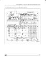
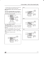
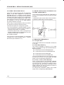
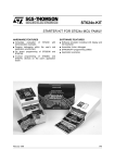
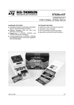
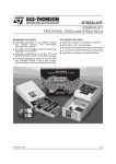
ST624xB-EMU2 REAL TIME EMULATION DEVELOPMENT TOOLS FOR ST624x MCUs HARDWARE FEATURES ■ Supports ST62 and ST63 family ■ Real time emulation ■ 32 KBytes of emulation memory ■ Breakpoint on a single address or on an address area ■ Break events can be defined on Program Space, Data space mixed with up to 4 external signals ■ 2 full programmable output for synchronisation ■ Read/Write registers on the fly (without wait state) ■ Selective trace in Range or Start/Stop ■ Break on Stack Overflow ■ 1K of real trace memory ■ Tracing of up to 32 bits including 4 external signals SOFTWARE FEATURES ■ Symbolic debugger at source level ■ On-line assembler/disassembler ■ Log files capable of storing any displayed screen ■ Command files able to execute a set of debugger commands July 1998 This is advance information from STMicroelectronics. Details are subject to change without notice. 1/21 5 Table of Contents ST624xB-EMU2 . . . . . . . . . . . . . . . . . . . . . . . . . . . . . . . . . . . . . .1 1 DELIVERY CHECK . . . . . . . . . . . . . . . . . . . . . . . . . . . . . . . . . . . . . . . . . . . . . . . . . . . . . . . . . . . .4 2 ST6 HDS2 NEW MAINFRAME EMULATOR . . . . . . . . . . . . . . . . . . . . . . . . . . . . . . . . . . . . . . . . 5 2.1 MAIN BOARD . . . . . . . . . . . . . . . . . . . . . . . . . . . . . . . . . . . . . . . . . . . . . . . . . . . . . . . . . . .6 2.2 ST6 HDS2 MAIN BOARD . . . . . . . . . . . . . . . . . . . . . . . . . . . . . . . . . . . . . . . . . . . . . . . . . .6 2.2.1 External output: OUT1 and OUT2 . . . . . . . . . . . . . . . . . . . . . . . . . . . . . . . . . . . . . . . 6 2.2.2 Data acquisition signals . . . . . . . . . . . . . . . . . . . . . . . . . . . . . . . . . . . . . . . . . . . . . . 7 2.2.3 LEDs RUN, STOP, WAIT . . . . . . . . . . . . . . . . . . . . . . . . . . . . . . . . . . . . . . . . . . . . . 7 2.3 INSTALLING AN ST6 EMU2 DEVELOPMENT TOOL. . . . . . . . . . . . . . . . . . . . . . . . . . . . . 7 2.4 INSTALLING A DEDICATION BOARD IN AN ST6 HDS2 . . . . . . . . . . . . . . . . . . . . . . . . . . 7 2.5 COMPONENTS LAYOUT OF ST6 MAIN BOARD (MB097) . . . . . . . . . . . . . . . . . . . . . . . . 8 2.6 COMPONENTS LAYOUT OF ST6 MAIN BOARD (MB174) . . . . . . . . . . . . . . . . . . . . . . . . 9 3 ST6 MAINFRAME EMULATOR (FIRST GENERATION) . . . . . . . . . . . . . . . . . . . . . . . . . . . . . . 10 3.1 CLZ80 BOARD . . . . . . . . . . . . . . . . . . . . . . . . . . . . . . . . . . . . . . . . . . . . . . . . . . . . . . . . . .10 3.2 GPFM/3 BOARD . . . . . . . . . . . . . . . . . . . . . . . . . . . . . . . . . . . . . . . . . . . . . . . . . . . . . . . .10 3.3 INTERFACE BOARD . . . . . . . . . . . . . . . . . . . . . . . . . . . . . . . . . . . . . . . . . . . . . . . . . . . . .11 3.4 INSTALLING AN ST6 HDS1 DEVELOPMENT TOOL . . . . . . . . . . . . . . . . . . . . . . . . . . . . 11 3.5 INSTALLING A DEDICATION BOARD IN AN HDS1 DEVELOPMENT TOOL . . . . . . . . . 11 4 DEDICATION BOARD (DBE) . . . . . . . . . . . . . . . . . . . . . . . . . . . . . . . . . . . . . . . . . . . . . . . . . . .12 4.1 VOLTAGE FUNCTIONING RANGE. . . . . . . . . . . . . . . . . . . . . . . . . . . . . . . . . . . . . . . . . . 12 4.2 JUMPER DESCRIPTION ON DEDICATION BOARD . . . . . . . . . . . . . . . . . . . . . . . . . . . . 13 4.2.1 VAPLI-PULLUP: default value on output buffers W11 . . . . . . . . . . . . . . . . . . . . . . 13 4.2.2 Clock Source Selection: W2 . . . . . . . . . . . . . . . . . . . . . . . . . . . . . . . . . . . . . . . . . . 13 4.2.3 Reset delay duration: W3 . . . . . . . . . . . . . . . . . . . . . . . . . . . . . . . . . . . . . . . . . . . . 13 4.2.4 Mask option on Timer 1: W4 named PUPTIM1. . . . . . . . . . . . . . . . . . . . . . . . . . . . 13 4.2.5 Bank RAM/EEPROM selection: W4 named RPG0, RPG1 . . . . . . . . . . . . . . . . . . . 14 4.2.6 ROM Program Size selection: option on W5 named ROM. . . . . . . . . . . . . . . . . . . 14 4.2.7 Timer 2 Enable/Disable: option on W5 named TIM2. . . . . . . . . . . . . . . . . . . . . . . . 14 4.2.8 Watchdog: W5 named WD . . . . . . . . . . . . . . . . . . . . . . . . . . . . . . . . . . . . . . . . . . . 14 4.2.9 Mask option on NMI Input: W5 named PUPNMI. . . . . . . . . . . . . . . . . . . . . . . . . . . 14 4.2.10 Real Time Clock Enable/Disable: option on W5 named RTC. . . . . . . . . . . . . . . . . 14 4.2.11 Combiports, Real Time clock selection: W8, W9 . . . . . . . . . . . . . . . . . . . . . . . . . . 15 4.2.12 W1 (EPLD): reserved . . . . . . . . . . . . . . . . . . . . . . . . . . . . . . . . . . . . . . . . . . . . . . . 15 4.2.13 Internal Oscillator frequency selection: W6, W7 . . . . . . . . . . . . . . . . . . . . . . . 21 . . . . 15 2/21 6 Table of Contents 4.3 PROBE: THE SCHRINK DIP 56 . . . . . . . . . . . . . . . . . . . . . . . . . . . . . . . . . . . . . . . . . . . . 16 4.4 PROBE: INSTALLING THE FERRITE COIL FOR EMC COMPATIBILITY . . . . . . . . . . . . 16 4.5 EMULATED PERIPHERALS . . . . . . . . . . . . . . . . . . . . . . . . . . . . . . . . . . . . . . . . . . . . . . . 16 4.5.1 Program Rom . . . . . . . . . . . . . . . . . . . . . . . . . . . . . . . . . . . . . . . . . . . . . . . . . . . . .16 4.5.2 Data Space Memory . . . . . . . . . . . . . . . . . . . . . . . . . . . . . . . . . . . . . . . . . . . . . . . . 16 4.5.3 Timer 1, Timer 2, SPI, Watchdog . . . . . . . . . . . . . . . . . . . . . . . . . . . . . . . . . . . . . . 16 4.5.4 Analog to Digital Converter . . . . . . . . . . . . . . . . . . . . . . . . . . . . . . . . . . . . . . . . . . . 17 4.5.5 Port A . . . . . . . . . . . . . . . . . . . . . . . . . . . . . . . . . . . . . . . . . . . . . . . . . . . . . . . . . . .17 4.5.6 Port B . . . . . . . . . . . . . . . . . . . . . . . . . . . . . . . . . . . . . . . . . . . . . . . . . . . . . . . . . . .17 4.5.7 Port C: combiports. . . . . . . . . . . . . . . . . . . . . . . . . . . . . . . . . . . . . . . . . . . . . . . . . .17 4.5.8 32 Khz Oscillator . . . . . . . . . . . . . . . . . . . . . . . . . . . . . . . . . . . . . . . . . . . . . . . . . . .18 4.5.9 LCD DRIVER . . . . . . . . . . . . . . . . . . . . . . . . . . . . . . . . . . . . . . . . . . . . . . . . . . . . .18 5 TROUBLESHOOTING . . . . . . . . . . . . . . . . . . . . . . . . . . . . . . . . . . . . . . . . . . . . . . . . . . . . . . . .19 5.1 AT POWER UP . . . . . . . . . . . . . . . . . . . . . . . . . . . . . . . . . . . . . . . . . . . . . . . . . . . . . . . . .19 5.2 DURING EMULATION: PROBLEM WITH PROGRAM COUNTER . . . . . . . . . . . . . . . . . 19 5.3 RESET EMULTATION IN REAL TIME. . . . . . . . . . . . . . . . . . . . . . . . . . . . . . . . . . . . . . . . 19 5.4 DISCREPANCIES BETWEEN EMULATOR AND ROM OR EPROM DEVICE. . . . . . . . . 19 5.5 AVOID THE MOST FREQUENT PROBLEMS WHEN PROGRAMMING ST6 MICROS!. 20 5.5.1 Execution of Interrupt . . . . . . . . . . . . . . . . . . . . . . . . . . . . . . . . . . . . . . . . . . . . . . . 20 5.5.2 Execution of WAIT and STOP instructions . . . . . . . . . . . . . . . . . . . . . . . . . . . . . . . 20 3/21 7 ST624xB-EMU2 - DELIVERY CHECK 1 DELIVERY CHECK This development tool is able to emulate all components belonging to the ST624BX family, it is able also to emulate the old ST624X family devices. The choice of emulated ROM Device is made either by properly setting the configuration on the dedication board or by software when using the new Debugger WGDB6 under WindowsTM, and by connecting the appropriate PROBE on the dedication board through the flat cables. When receiving a whole ST624XB development tool or a ST624XB-DBE please refer to the 4/21 8 “PRODUCT DELIVERY” to check the content of the package. Instructions for use - Warning This development tool conforms with the EN55022 emissions standard for ITE, and with generic 50082-1 immunity standards. Then, it complies with the 89/336/EEC directive. The product is a A Class apparatus. In a residential environment this device may cause radioelectrical disturbance which may require that the user adopts appropriate precautions. ST624xB-EMU2 - ST6 HDS2 NEW MAINFRAME EMULATOR 2 ST6 HDS2 NEW MAINFRAME EMULATOR The new ST6 HDS2 mainframe (with MB097 main Board) has been designed to replace the HDS1 version. The main modifications are: – Communication transfer rate: it is now much faster thanks to the use of parallel port. – Dimension and weight: the old 3 boards, basic part of the system, have been redesigned in one board. – The cost of the overall system has been well reduced. In the second version of ST6 HDS2, (metal box with MB174 main Board) modified for CEM conformity, these new features have been introduced: – Read/ Write registers on the fly during execution of program without any wait state. – Selective record of bus in logical analyser in Range or Start/Stop mode. – Output OUT1 and OUT2 for synchronisation of an external equipment, programmable in the same way as Selective trace, in Range or Start/ Stop mode. – Stack overflow: a break is automatically generated (by default) in case of stack overflow. – Break execution: in this new version, the program stops before the execution of the fetch. These main frame consist of a basic part, common to all ST6 devices, and one ST62 or ST63 sub family dedicated board depending on the specific device to emulate. This new emulator is full compatible with existing dedicated boards, excepting ST631XX-DBE which have been designed in 2 boards. Only the dedicated board has to be changed to emulate a new device within the ST62/ST63 sub families. The use of parallel port allows a very faster communication transfer rate. The symbolic debugger, software part of the real time emulation tool, can be run on a PC, and is common to all ST62 and ST63 devices. The debugger uses a windowed menu driven interface, and enables the user to set the configuration of the emulator. Figure 1. Hardware Development System Emulator HARDWARE DEVELOPMENT SYSTEM EMULATOR (HDS2) Parallel Port connection Dedication Board Power OUT-1 OUT-2 Stop Wait Run 4 3 2 1 Triggers ST6 HDS2 EMULATOR (.EMU2) ST6 probe 5/21 9 ST624xB-EMU2 - ST6 HDS2 NEW MAINFRAME EMULATOR 2.1 MAIN BOARD The Main board controls the emulator thanks to a ST9 central processing unit which executes commands coming from host computer through the parallel line. The board contains all emulation resources, the core of the ST6, the Program ROM emulation, the break point logic, the trace memory, the automaton and all necessary logic for a real time emulation. Two connectors, J1 and J2, are used to exchange signals with the dedication board. The amount of program memory in the main board is factory set at 32k, in fact the size of the memory depends on the dedication board, which contains the Program Rom Pagination Register (PRPR) if it exists (no PRPR for memory size lower than 4k). No configuration jumpers are required. 2.2 ST6 HDS2 MAIN BOARD On the rear panel there is: – a power plug to connect power: 5 Volts 3 Amp min. (The delivered power is 100 volts to 240 volts input and 5 Amp output). – a power switch. – a parallel connector for an IBM PC(TM) compatible. On front panel: – a led “POWER ON” signal. – OUT 1 and OUT 2 signals which can be used for synchronizing an external equipment. – 2 leds indicating when the ST6 core is in “STOP” or “WAIT” mode. – a 16 pin connector for data acquisition signals. The explanation of these signals is done in the debugger manual. 6/21 10 2.2.1 External output: OUT1 and OUT2 For debugging hardware it is very useful to have synchronization signals. The goal of the outputs 1 and 2 is to offer this feature to the user. They can be programmed differently whether the debugger used is the DOS debugger ST6NDB or the Source Level Debugger WGDB6, as explained in the two following paragraph. They are full programmable with WGDB6. Output OUT1 and OUT2 under ST6NDB When using old DOS Version of debugger ST6NDB: This feature is programmable thanks to Hardware Breakpoint Menu. The breakpoint MENU allows to define breaking events. These events will generate an actual breakpoint only if break enable is ON. When break is off, these events are existing in the development tool. In the HDS2 emulator version up to 4.3, the signals OUT1 and OUT2 are connected to these internal breaking events. Therefore these signals can be used to synchronize an external device while running (breakpoint off). Output OUT1 and OUT2 under WGDB6 When using WGDB6 new Version of debugger at source level under WindowsTM: This feature is full programmable thanks to Hardware Events/Trigger Menu. Output OUT1 and OUT2 can be programmed in two ways: – Events for synchronisation: it allows to the user to preset pulses synchronisation for an external equipment. The events can be defined by addresses or by range of addresses. – Events for Timing Measure: it allows to the user to measure time elapsed during a subroutine for example. In this case, output OUT2 is SET on a user defined address, and RESET on an other one, OUT1 is the ST6 clock cycle gated by OUT2. These 2 functioning modes are clearly displayed on screen. ST624xB-EMU2 - ST6 HDS2 NEW MAINFRAME EMULATOR 2.2.2 Data acquisition signals In a same way as are recorded Buses, Flags, Bank registers in the trace memory, the ST6 HDS2 offers the possibility to record 4 external signals. These signals must be connected on the pin 1,3,5,7 of the Analyser probe connector on the front panel of the HDS2, as shown below. A flat cable with probe tip is delivered with the emulator. These inputs are CMOS compatible at 5 Volts . VCC Caution: +5V EMU 2.3 INSTALLING AN ST6 EMU2 DEVELOPMENT TOOL GND 1 AL3 – There is no clock: see chapter about clock source selection. After a correct initialisation: When user’s program is running (in real time), led RUN is on. When ST6 core is in WAIT mode, led WAIT is ON. When ST6 core is in STOP mode, both leds STOP and WAIT are ON. AL2 AL1 AL0 2.2.3 LEDs RUN, STOP, WAIT Three leds have been added to indicate to the user the state of the core or of the development tool during emulation. First at power up, the red led is ON and becomes OFF after a few time. It lights one short time during connection establishment between ST6 HDS2 emulator and host computer. After that, the Run led must be OFF. If the LED RUN remains ON after power up, it will cause a default in initialisation of emulator, this default can be caused by: – The emulation is in Reset: if the emulator is connected on a target application, this application must have been powered before. – When receiving a whole development tool, the dedication board is delivered inside the mainframe. – You have just to: – connect the power supply to the mains(100 to 240 volts). – connect the output (5Volts) of power supply on the DIN connector of the rear panel – connect the parallel cable between the parallel connector and the host computer. For installing the probe, please refer to the appropriate item in the Dedication Board chapter. 2.4 INSTALLING A DEDICATION BOARD IN AN ST6 HDS2 If there is already a dedication board in the development tool, you have simply to: – unscrew the 2 screws on each side of the dedication board, and press outward on the release buttons to extract the board. Then insert the new dedication board in the guide rods and push it hardly in the backplane, and: – screw the 2 screws on each side of the dedication board. For installing the probe, please refer to the chapter “Installing the probe”. 7/21 11 ST624xB-EMU2 - ST6 HDS2 NEW MAINFRAME EMULATOR 2.5 COMPONENTS LAYOUT OF ST6 MAIN BOARD (MB097) VR02091A 8/21 12 ST624xB-EMU2 - ST6 HDS2 NEW MAINFRAME EMULATOR 2.6 COMPONENTS LAYOUT OF ST6 MAIN BOARD (MB174) VR02091U 9/21 13 ST624xB-EMU2 - ST6 MAINFRAME EMULATOR (FIRST GENERATION) 3 ST6 MAINFRAME EMULATOR (FIRST GENERATION) The ST6 mainframe emulator contains positions for 5 boards : – CLZ80 board must be inserted on the first (bottom) position – GPFM/3 board must be on second position – interface N (DB014) must be inserted on third position – dedication board ST638X (MB167) inserted in one of the two top position On the rear panel there is : – a main-power selector to select 110 volts or 220 volts. – a power plug – a power switch On front panel : – the RS232 connector to link the emulator with an IBM PC – EXT-SIG connector that allows you to choose between 3 groups of 4 signals to be memorize on trace memory. These signals are independent from the probe data acquisition signals. The explanation of these signals is done in the debugger manual – Z80 reset push button – ST6 INT push-button 3.1 CLZ80 BOARD The CLZ80 board controls the mainframe emulator and it is linked to an IBM PC through an RS232 line. On this board only 2 connectors are used : 10/21 14 – J5 connected to the front panel RS232 25 pin connector – J4 connected to the front panel Z80-RESET push-button 3.2 GPFM/3 BOARD GPFM/3 board contains the emulation resources : Program ROM emulation, break point, trace memory. Two connectors, J3 and J4, are used to exchange signals with the interface board. When emulating ST62XX or ST63XX, the interface board is an N-WELL interface board. The two connectors are used. For emulating components of other families, the interface board can be a P-WELL interface board: in this case only one connector is used, the jumpers of W2 must be plugged. JUMPERS SETTING for ST62XX and ST63XX emulation: W1: All jumpers must be removed. W2 : One jumper only must be set to link pin 1 to pin 16. CONNECTORS : J3 and J4 : Used to link this board with the N-WELL interface board. J5 : Used to connect the data acquisition probe. ST624xB-EMU2 - ST6 MAINFRAME EMULATOR (FIRST GENERATION) 3.3 INTERFACE BOARD The interface board emulates the CPU-core. JUMPERS SETTINGS: S1: – not used in emulation mode – allows the definition of the type of EPROM (27256/27128) used in stand-alone (without CLZ80 and GPFM/3 boards) mode S2, S3: size of emulation program ROM The position reference names depend on the version of the board. For S2 they can be identified as 0 and 1 or OLD and NEW on the board. For S3 it can be 0 and 1 or 4K and 8K. S2 S3 Size 0 or OLD 0 or 4K 4K 0 or OLD 1 or 8K 8K 1 or NEW 0 or 4K 16K 1 or NEW 1 or 8K 32K Comment normal setting not supported The purpose of this jumper is to allow the emulator to check the amount of emulation program ROM that is used. TEST/NO TEST: must be in NO TEST position CONNECTORS: J1 and J4 to link this board to GPFM/3 board. J2: receives signals from J1-EXT SIG. connector situated on the front panel of the ST6 emulator. J3: is connected to ST6-RESET, ST6-INT pushbuttons, STOP-LED and WAIT-LED situated on the front panel of the ST6 emulator. 3.4 INSTALLING AN ST6 HDS1 DEVELOPMENT TOOL When receiving a whole development tool, the dedication board is delivered inside the mainframe, it is plugged in one of the two top position in the backplane. – First of all, it is mandatory to verify the mainframe: – remove the 2 screws on the rear panel of the main frame – lift the lid on the side of the rear panel – pull the lid from the rear panel, it dissociates it from the front panel – remove the lid, pay attention to the wire for the ground connection Verify that all boards are correctly inserted in the backplane of the mainframe in the right order: – CLZ80 board must be inserted on the first (bottom) position – GPFM/3 board must be on second position – Interface N (DB014) must be inserted on third position – The two top positions are intended to receive one or a couple of dedication boards in order to emulate one family of components: in this case, only the new DBE board must be in one of the two top positions. For installing the probe, please refer to the appropriate chapter in the Dedication Board part. After installation of a probe, the flat cables must be parallel. 3.5 INSTALLING A DEDICATION BOARD IN AN HDS1 DEVELOPMENT TOOL When receiving only a dedication board, this board must be installed as described below. Open the main frame by removing the lid: – remove the 2 screws on the rear panel of the main frame – lift the lid on the side of the rear panel – pull the lid from the rear panel, it dissociates it from the front panel – remove the lid, pay attention to the wire for the ground connection Then remove the dedication board or the two dedication board which are plugged in the two top position of the backplane. After that, plug the new dedication board in one of the two top positions of the backplane. For installing the probe, please refer to the appropriate item in the Dedication Board chapter. 11/21 15 ST624xB-EMU2 - DEDICATION BOARD (DBE) 4 DEDICATION BOARD (DBE) This board contains the specific functions for ST624X emulation: – EEPROM (Byte mode and parallel mode) – RAM – Timer 1 – Timer 2 – Watchdog – Analog to Digital Converter – Serial Peripheral Interface – Analog to Digital Converter – Port A: 8 Bits – Port B: 8 Bits – Port C: 8 Bits (Combiports) in alternate function with LCD segments – 32 Khz oscillator – LCD Driver – Power Supply Supervisor – External non Maskable Interrupt – Pagination Registers A white dot indicates the position 1 for all jumpers and components on the board. Note for the VCC pin: When the input power pin VCC is connected, this input is used as a reference voltage by the emulator.(please refer to the 5-1 chapter) 12/21 16 No power is given or taken at this pin by the emulator. Notes on write-only registers: Several Data Space registers of the emulated ROM device are write-only, however, to offer more flexibility to the user, they are readable when commands such as “watching register” are used. 4.1 VOLTAGE FUNCTIONING RANGE The new ST624XB-DBE board has been designed to emulate the ROM device in the range of 3 to 6 Volts. When the input power VCC pin is connected, this input is used as a reference voltage by the emulator. This reference voltage is amplified thanks to an operational amplifier and an emitter follower for powering the output buffers, and for giving the high reference voltage to the ADC and the Power Supply Supervisor. Then all the outputs of the peripherals are fully compatible at CMOS level with an application which is powered in the range from 3 to 6 Volts. When VCC Pin is not connected, it is mandatory to close W11 Jumper (see 5.2 chapter) in order to power all buffers with 5 volts, it permits to use emulator without target application. No power is given nor taken at this pin by the emulator. ST624xB-EMU2 - DEDICATION BOARD (DBE) 4.2 JUMPER DESCRIPTION ON DEDICATION BOARD Jumpers on the board are used to select the amount of Data Space MEMORY, the emulated PERIPHERALS, and metal MASK OPTION of the ROM device. After powering the system, the options taken in account by the DBE are the jumpers of the board. Thanks to the new debugger WGDB6 under windowsTM, the options can be either the set of jumpers on board, or options chosen by software. In the menu command then submenumicroconfiguration, the user can chose new options and then select Software configuration, or eventually return to the hardware configuration. The difference between the ROM devices belonging to the ST624X family are as follow: – The ST6240 is the most powerful device, it contains all peripherals, and all possible resources are bounded on pins. – The ST6242, ST6245 and ST6246 are subsets of ST6240, some peripherals are not available, some resources are not bounded and the amount of Program and Data Space memory is different. To emulate a specific Device, the user must set options according to the data sheet of this device. When a peripheral is not used, for example Timer 2 for ST6242, registers of this peripheral are at zero value, and they cannot be written. This chapter explains how to select these features. 4.2.1 VAPLI-PULLUP: default value on output buffers W11 When VCC Pin is not connected, it is mandatory to close W11 Jumper in order to power all buffers with 5 volts, it permits to use emulator without target application. When the probe is on the target application the pullup resistor can intruce an error particularly when using A/D converter (High reference of A/D is VCC). 4.2.2 Clock Source Selection: W2 The system CLOCK can be chosen between internal oscillator and clock issued from the probe. This jumper setting is clearly printed on board, with INT for INTERNAL clock and EXT for clock issued from the probe. If the jumper is connected between: 1-2 In this case the clock of the probe is selected 2-3 (factory setting) The internal clock is selected. In this case the internal clock is made thanks to an oscillator with a 8 MHz crystal. Note for CLOCK “issued from the probe”: If the user uses a probe made by SGS-THOMSON, this probe is able to send a clock to the dedication board in two ways: – a clock made by the on board oscillator on the probe. – a clock directly issued from the application. In this case the signal on OSCIN must be at CMOS level. For more details, please refer to the ST6246 probe chapter or to the documentation delivered with the QFP probe. WARNING on probe on board oscillator: – QFP Probes: Because of parasitic capacitors due to connections, it is mandatory to not use the on board oscillator of the QFP Probes, or eventually to adapt components to the application, and verify the signal with an oscilloscope. – ST6246B (SDIL56) probe: this board has been designed to avoid the problem of parasitic capacitors: the “open” schematic permits to the user to reconstruct on the probe, the same oscillator as on his own application. The probe is able to support a crystal or a resonator 3 pins with or without capacitor, it can be of course used also with an RC. 4.2.3 Reset delay duration: W3 For as long as the reset pin is kept at the low level, the processor remains in the reset state. After the pin reset has been released, a counter provides a delay between the detection of the reset high level and the release of the MCU reset: the jumper on W3 named buildup counter permits to select the duration of this delay. The standard delay is 2048 oscillator cycles: the jumper must be in front of 2 (factory setting). For delay of 4096, 8192 or 16384 the jumper must be in front of respectively 4, 8, or 16, clearly printed on the board. 4.2.4 Mask option on Timer 1: W4 named PUPTIM1 The pin of the timer 1 can be pulled up by a 100k resistor. This resistor is connected to the timer 1 input by a jumper named PUPTIM1 on W4 selector. – If Jumper PUPTIM1 is on the side “EN”: Timer pin is pulled up by 100k. – If Jumper PUPTIM1 is on the side “DIS”: Timer pin is not pulled up. 13/21 17 ST624xB-EMU2 - DEDICATION BOARD (DBE) 4.2.5 Bank RAM/EEPROM selection: W4 named RPG0, RPG1 If the user wants to be sure to not use to much of available memory RAM according to his chosen device, he can ENable/DISable indepently the 4 bits of Data RAM/EEPROM Bank register: DRBR. The factory Jumper setting corresponds to the most powerful device. For EEPROM: – If Jumper EPG0 (EEPROM page 0) is on the side “EN”: Bit 0 of DRBR is valid (01). – If Jumper EPG1 (EEPROM page 1) is on the side “EN”: Bit 1 of DRBR is valid(02). For RAM: – If Jumper RPG1 (RAM page 1) is on the side “EN”: Bit 3 of DRBR is valid (08H). – If Jumper RPG2 (RAM page 2) is on the side “EN”: Bit 4 of DRBR is valid (010H). If Jumper is on the side DISable, the corresponding Bit is forced to “0”, causing an non access to memory. 4.2.6 ROM Program Size selection: option on W5 named ROM If the user wants to be sure to not use to much of available memory ROM according to his chosen device, he can select the “small” size of memory: 4K. The ROM memory size is set thanks to W5 selector on part named ROM: – If Jumper ROM is on the side “4K”: the amount of available ROM is 4K. – If Jumper ROM is on the side “8K”: the amount of available ROM is 8K.(Factory setting) When program memory size is 4 k Bytes, it means that all bits of Program Rom Pagination Register are at zero value and are not able to be written. When program memory size is valid up to 8 k Bytes: it means that Bit 0 and 1 of Program Rom Pagination Register are available. 14/21 18 4.2.7 Timer 2 Enable/Disable: option on W5 named TIM2 The explanation of W5 selector, is explained clearly on the board, on the left side, when regarding the front panel of the board. ENABLE DISABLE TIM2 WD H PUPNMI RTC ROM 4K S 8K W5 W5 If the user wants to be sure to not use the Timer 2, case of emulating the ST6242 device, the user must set the jumper on DISable position. The option Enabling/Disabling the Timer 2 is set thanks to W5 selector on part named TIM2: – If Jumper TIM2 is on the side “EN”: Timer 2 is valid. – If Jumper TIM2 is on the side “DIS”: Timer 2 is not valid, its registers remain at reset state. 4.2.8 Watchdog: W5 named WD The explanation of W5 selector, is explained clearly on the board, on the left side, when regarding the front panel of the board. For the ST624X family, this option is not used, because the current devices have a dedicated input. The dedicated input exists for ST6240 device, but is internally pulled up for others devices, it is corresponding to SOFTWARE WATCHDOG. 4.2.9 Mask option on NMI Input: W5 named PUPNMI The NMI Input can be pulled up by a 100k resistor. This resistor is connected to the NMI input by a jumper named PUPTIM1 on W5 selector. – If Jumper PUPNMI is on the side “EN”: NMI input is pulled up by 100k. – If Jumper PUPNMI is on the side “DIS”: NMI Input is not pulled up. 4.2.10 Real Time Clock Enable/Disable: option on W5 named RTC The option Enabling/Disabling the RTC is set thanks to W5 selector on part named RTC: – If Jumper RTC is on the side “EN”: RTC is valid. ST624xB-EMU2 - DEDICATION BOARD (DBE) 4 MHz W6 CLK8/2 4/1 CLK8/4 2/1 W6 – If Jumper RTC is on the side “DIS”: RTC is not valid, its registers remain at reset state. 4.2.11 Combiports, Real Time clock selection: W8, W9 The option Enabling/Disabling the Combiports or the RTC is set thanks to W8 and W9 jumpers: The figure below shows the Factory setting for these jumpers, which is Enable. A CLK8/4 2/1 W9 4/1 W6 CLK8/2 W7 B W8 A 2 MHz W9 B W9 W6 DISable ENable 4/1 CLK8/4 2/1 A W7 W9 B 1 MHz W6 CLK8/2 4/1 CLK8/4 2/1 W6 4.2.12 W1 (EPLD): reserved This jumper is reserved for a future use, therefore it must be on LOW. 4.2.13 Internal Oscillator frequency selection: W6, W7 The new ST624XB-DBE offers to the user to chose an internal frequency lower than 8 MHz. The 4 possibilities are: 1MHz, 2 MHz, 4MHz, 8MHz. The selection is made as below: 8 MHz CLK8/2 W6 PSS or Combiport A 4/1 CLK8/4 2/1 W6 CLK8/2 A W7 W7 W9 B B W9 W6 15/21 19 ST624xB-EMU2 - DEDICATION BOARD (DBE) 4.3 PROBE: THE SCHRINK DIP 56 This probe is always delivered with the Dedication Board. It has been designed to emulate the ST6246B device or a subset of same footprint. With this new probe, it is possible to recontitute an oscillator at the same frequency as on application: an on board oscillator, designed in an “open” schematic permits to place on the probe, the Crystal or the resonator or an RC as on target application.(see schematic in Annex). When using clock generated by probe, the dedication board must be set in EXTernal clock. Two Selectors permit to configure the probe: W1: Choice between on board oscillator or Oscin. – If the user wants to use the on board oscillator he must place the jumper on: Oscillator. – If the user wants to use a clock coming from application at CMOS level on OSCIN input: the user must place the jumper on OSCIN. W2: Disable oscillator If the user do not use the oscillator, it is preferable to disable it for noise and EMC reason. (Jumper W2 forces input oscillator to “0”) 4.4 PROBE: INSTALLING THE FERRITE COIL FOR EMC COMPATIBILITY To be conform to the EMC directive, particularly in emission, the delivered ferrite coil must be placed as follow: 1) Place each part on each side of the flat cables 2) Place the metal clip to fix them together 1 2 2 ST6 probe 1 4.5 EMULATED PERIPHERALS 4.5.1 Program Rom The program ROM size for ST624XB or ST624X is 4 K or 8 K. 4.5.2 Data Space Memory The memory available in range 0 to 3F in data space, is accessed through the Data Ram/Eeprom Banking Register: Bit 0 if set selects the first EEPROM bank Bit 1 if set selects the second EEPROM bank Bit 3 if set selects the first RAM bank Bit 4 if set selects the second RAM bank. Care must be taken that only one of these four bit must be set at a time, for more details see Data Sheet of the corresponding ROM device. 4.5.3 Timer 1, Timer 2, SPI, Watchdog Clock of these devices are voluntarily validated only during emulation, it provides to see the evolving values of them. Therefore pay attention that in Step by Step mode the values of counters can be slightly different of a real time session because of setting ON and OFF emulation. For using these peripherals, please, refer to data sheet of the corresponding ROM DEVICE. 16/21 20 ST624xB-EMU2 - DEDICATION BOARD (DBE) 4.5.4 Analog to Digital Converter This peripheral is available on A port and Bit 0 to 3 of B port. The ADC input can be connected at one of the 12 inputs, the 8 of port A and the 4 of port B, by properly programming the registers of these ports (one at a time). If more than one ADC input are selected, they will be short circuited each other’s. This feature can be eventually used for multiplexing analog signals. The analog to Digital Converter converts the input value in about 70µS at 8 MHz of Xtal clock. Clock conversion is always present, it means that a data conversion is always accomplished after writing a start conversion even if it is executed in Step mode of emulation. It allows to the user to convert analog input step by step. Note on ADC voltage reference: The high voltage reference for the ADC is the applied voltage on the pin VCC internally buffered in the board. The low voltage reference is the GROUND. Then to have a conversion result of 0FFH, the voltage at the analog input must be equal to the voltage of the VCC pin. 4.5.5 Port A The functioning mode of each bit of this 8 bits port is selected by properly programming the three associated registers: Data Register (DRA), Data Direction Register (DDRA), and Option Register (ORA) as follow. DDR OPR DR 0 0 1 0 0 0 1 1 1 0 1 1 0 0 0 1 X X I/O Mode Input without pullup, interrupt disabled Input with pullup, interrupt enabled Input with pullup, interrupt disabled Analog Input Push Pull Output Open Drain NMOS output Beware of mixing input and output modes in the same port, in this case, do not use SET or RES instructions on Data Registers: When a port bit is in input mode, the data read is the state of the pin of the device (or the probe); when a port bit is in output mode the data read is the data register, so when using a read/modify/ write instruction, a bit port mode can be changed from input mode to analog input mode unintentionally! For more details about this peripheral, please, refer to Data Sheet of the corresponding ROM Device. 4.5.6 Port B The functioning mode of each bit of this 8 bits port is selected by properly programming the three associated registers: Data Register (DRB), Data Direction Register (DDRB), and Option Register (ORB) as follow. Note that only the four bits PB0 to PB3 can be ADC inputs. DDR OPR DR 0 X 1 0 0 0 1 1 1 0 1 1 0 0 0 1 X X I/O Mode Input with out pullup, interrupt disabled (PB4to7) Input with pullup, interrupt enabled Input with pullup, interrupt disabled Analog Input (only for PB0 to 3) Push Pull Output Open Drain NMOS output Beware of mixing input and output modes in the same port, in this case do not use SET or RES instructions on Data Registers: When a port bit is in input mode, the data read is the state of the pin of the device (or the probe); when a port bit is in output mode the data read is the data register, so when using a read/modify/ write instruction, a bit port mode can be changed from input mode to analog input mode unintentionally!. For more details about this peripheral, please, refer to Data Sheet of the corresponding ROM Device. 4.5.7 Port C: combiports. The functioning mode of each bit of this 8 bits port is selected by properly programming the three associated registers: Data Register (DRB), Data Direction Register (DDRB), and Option Register (ORB) as follow. Note: The alternate function on the 8 Input/Output of this port are 8 segments output (S33 to S40) of the Liquid Crystal Display driver. For ST624X compatibility (combiport more), OPR and DR are set to 1 after Reset, same as in the device. DDR OPR DR 0 0 1 0 1 0 I/O Mode Input without pullup, interrupt disabled Input with pullup, interrupt enabled 0 0 1 1 0 1 1 0 0 1 X X Input with pullup, interrupt disabled Output S33 to S40 of LCD Driver Push Pull Output Open Drain NMOS output 17/21 21 ST624xB-EMU2 - DEDICATION BOARD (DBE) Beware of mixing input and output modes in the same port, in this case do not use SET or RES instructions on Data Registers: When a port bit is in input mode, the data read is the state of the pin of the device (or the probe); when a port bit is in output mode the data read is the data register, so when using a read/modify/ write instruction, a bit port mode can be changed from input mode to analog input mode unintentionally!. For more details about this peripheral, please, refer to Data Sheet of the corresponding ROM Device. 4.5.8 32 Khz Oscillator It is mandatory to use this peripheral in real time mode with the development tool, because its 18/21 22 clock input is always available even in STEP mode. For more details about this peripheral, please, refer to Data Sheet of the corresponding ROM Device. 4.5.9 LCD DRIVER The LCD driver is directly emulated with a ST6240 microcomputer. The ST6240 reads permanently the LCD RAM and writes in its own corresponding RAM. For more details about this peripheral, please, refer to Data Sheet of the corresponding ROM Device. ST624xB-EMU2 - TROUBLESHOOTING 5 TROUBLESHOOTING 5.1 AT POWER UP At the beginning of an emulation session, on screen of PC must appear the debugger message up to the end of software connection establishment. If a ”TIMEOUT” message is encountered, there is a connection problem, which can come from one of these reasons: with ST6HDS2 – ST6 development Tool is not power ON – The parallel line is not well connected or with old main frame: – verify that the delivered cable is actually connected directly to the Main Frame. – and if necessary there is another cable which is either a ”wire to wire” connection or an 25 to 9 pin adaptor. – The serial line is not connected the right I/O port of the computer. 5.2 DURING EMULATION: PROBLEM WITH PROGRAM COUNTER In case of ”Check Hardware Jumpering” or wrongly executing code in step mode: Most of the time, this problem occurs with HDS1 emulator or with HDS2 plastic BOX up to 4.3 version, it is coming from that the development tool is in RESET state, it can be caused by: – The application where probe is connected is not powered on, then the schmitt trigger on pin Reset is active and causes the RESET – The pin Reset of emulated device is at low level – A probe is connected, but is not powered either by an application or by a voltage on the VCC input. For properly emulating RESET please refer to the following chapter. 5.3 RESET EMULTATION IN REAL TIME With ST6HDS2 new metal box, it is now possible to begin an emulation session even if application is off, it is required particularly in MONITOR or TV applications. With old ST6 HDS1 emulator, or with HDS2 plastic BOX up to 4.3 Version, if the application requires that software must be executed just after power ON, it is mandatory to proceed as follow: – not connect, or remove probe from application. – power ON emulator. – begin emulation session: load program. – then start execution of program in Real Time. – plug the probe in the application (which is off), at this time the ST6 emulator is in reset state, because Reset and VCC pins are at low level. – Power ON the application, then the execution of software will start. 5.4 DISCREPANCIES BETWEEN EMULATOR AND ROM OR EPROM DEVICE When some differences of behavior are appearing between the emulator and the ROM device, in most cases, it comes from using read/modify/write instructions on – registers in which some bits are writable, and some bits readable. For these registers, trouble are caused, because when reading, a random value is read by the CPU, after calculating the mask, this random value is written in the register, changing it unintentionally! The same problem can occur with registers, where some bits have a different function during writing or during reading. Example for Ports: When reading a bit port in input mode, the read value is the level of the pin. When reading a bit port in output, the read value is the value of the corresponding bit in the Data Register. In case of problems check if each used register is correctly accessed. The principle ST6 registers (depending on the family), with which care must be taken, are listed below: – The EEPROM control registers – The two control registers of the 2 SPIs – The Data registers of the 3 Ports A, B and C – Analog to Digital Converter Control Register – The Sync Processor – The 9 PWM D/A control registers – The 14 bits (PWM+BRM) D/A converter – The NMI/PWR/VSYNC Interrupt Register – The Interrupt Option Register – The Program Rom Pagination Registers 19/21 23 ST624xB-EMU2 - TROUBLESHOOTING – The Data RAM/EEPROM Banking Register – The Data ROM window Register To offer more flexibility to the user, all of these registers are readable outside of real time.(undefined bits are read as ”0” value). 5.5 AVOID THE MOST FREQUENT PROBLEMS WHEN PROGRAMMING ST6 MICROS! 5.5.1 Execution of Interrupt If interrupt are not executed, in most cases, it comes from: – The core is not in normal mode: after RESET the core is in NMI mode, to enter the normal mode which let execute interrupt, the core must execute a RETI instruction. – The global enable interrupt bit has not been SET, or has been unintentionally cleared, then the IOR register must be checked. The default value to enable Interrupts is 010H. 20/21 24 – The enable interrupt bit of the desired peripheral has not been SET, or has been unintentionally cleared. – The Interrupt Option Register is write only, and has been wrongly written by a read/modify/write instruction, only LDI is permitted. 5.5.2 Execution of WAIT and STOP instructions In WAIT mode, led WAIT is ON, in STOP mode the 2 led WAIT and STOP are ON (on the front panel of the emulator). If STOP or WAIT instructions are not exited, it comes from: – The core is not in normal mode: after RESET the core is in NMI mode, to enter the normal mode which let execute interrupt to exit from these states, the core must execute a RETI instruction. Explanation: the only way to go out of STOP or WAIT state is to have an INTERRUPT or a RESET, it is the reason why, to execute these instructions the interrupt must have been validated. ST624xB-EMU2 - TROUBLESHOOTING Notes: Information furnished is believed to be accurate and reliable. However, STMicroelectronics assumes no responsibility for the consequences of use of such information nor for any infringement of patents or other rights of third parties which may result from its use. No license is granted by implication or otherwise under any patent or patent rights of STMicroelectronics. Specifications mentioned in this publication are subject to change without notice. This publication supersedes and replaces all information previously supplied. STMicroelectronics products are not authorized for use as critical components in life support devices or systems without the express written approval of STMicroelectronics. The ST logo is a registered trademark of STMicroelectronics 1998 STMicroelectronics - All Rights Reserved. Purchase of I2 C Components by STMicroelectronics conveys a license under the Philips I2C Patent. Rights to use these components in an I2 C system is granted provided that the system conforms to the I2 C Standard Specification as defined by Philips. STMicroelectronics Group of Companies Australia - Brazil - Canada - China - France - Germany - Italy - Japan - Korea - Malaysia - Malta - Mexico - Morocco - The Netherlands Singapore - Spain - Sweden - Switzerland - Taiwan - Thailand - United Kingdom - U.S.A. http:/ /www.st.com 21/21