1
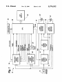
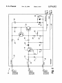
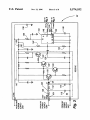
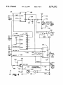
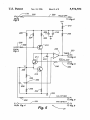
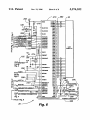
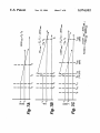
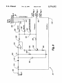
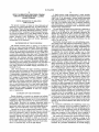
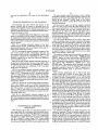
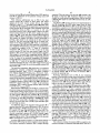
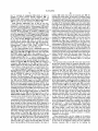
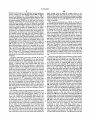
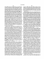
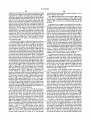
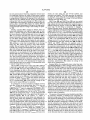
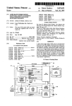
| l| l| |[11]l|l|l lPatent
l l l l l lNumber:
?u?l l l l l l l l l l l 5,574,552
llllllll
574552A
Ulllted States Patent [19]
Dunne
[54]
[45] Date of Patent:
Nov. 12, 1996
SELF-CALIBRATING PRECISION TIMING
5,157,403 10/1992 Urkowitz
.. 342/203
CIRCUIT AND METHOD FOR A LASER
5,359,404 lO/l994 Dunne ....................................... .. 356/5
RANGE FINDER
OTHER PUBLICATIONS
[75] Inventor: Jeremy G. Dunne, Littleton, Colo.
_
Pro Laser H’ Infrared Lidar System, User Manual p/N
_
006—0535—00, Kustom Signals, Inc. Chanute, Kansas, copy
[73] Assignee. Laser Technology, Inc., Englewood,
C010‘
right 1991’ pp_ 1_37_
ProLaser l1, Tra?ic Safety Lidar, Lidar System Functions,
Lidar System Speci?cations Brochure, Kustom .Signals,
Inc., Lenexa, KS, Feb. 1994, pp. 14.
[21] Appl- No: 375,941
22
-
[ ] Flled
[51]
..
Marksman LTI 20—20 Laser Speed Detection System,
.
Jan 19’ 1995
Operator’s Manual, Laser Technology, Inc., Englewood,
Int. Cl.6 ........................... .. G01C 3/08; GOlS 13/08;
Colorado, copyright 1994, pp. l-45.
601F366
.
.
.
P'
Exammer
' —Step h en CB
'ki
nmary
.
llCZlI‘lS
[52] US. Cl. ....................... .. 356/5.05, 342/134, 342/135,
342/202, 356/28
[58]
Attorney, Agent, or Fiml_winiam l Kubida; Holland &
Hart LLP
Field of Search ................................... .. 342/134-137,
342/202-204; 367/127; 356/5.01—5.08,
[57]
ABSTRACT
28
[56]
A highly precise range measurement instrument is made
possible through the use of a novel and e?‘icient precision
timing circuit which makes use of the instrument’s internal
central processing unit crystal oscillator. A multi-point cali
References Cited
U'S' PATENT DOCUMENTS
3,644,740
3,959,641
2/1972 Dobmtz et a1, _
5/1976 Miller, Jr, et a1. .
bration function includes the determination of a “zero” value
and a “cal” value through the addition of a known calibrated
4,214,242
7/1980 Colin.
pulse width thereby providing the origin and scale for
4,259,592
3/ 1981 Frungez et a1. .
determining distance with the constant linear discharge of
4,569,599
2/1986 Bolkow et a1. ....................... .. 368/120
capacitor‘
'
4,571,085. 2/1986 Anderson.
4,699,508
10/1987 [Bolkow et a1. .
4,770,526
9/1988 Manhart et a1. .
O V1 .
a
I
22 Claims, 8 Drawing Sheets
I
I
_'T—I\|
N V
'
2
l
l
l
I
I
I
l
I
T0 T1
a] V‘
-
T2
l
|
ZEROWTB-TO
v
\
l
a
+
7
3
TIME =
' ZERO'HME
=T8 ‘T3.
0V
LASER
(TX) (RX)
TIME ' ZERO-"ME )
CAL TIME ‘ ZEROTIME
US. Patent
Nov. 12, 1996
Sheet 2 of 8
5,574,552
m
w a:0b .mt
i
oh it
mm
vm
mm
Nm
mm.
mm
Om)
O
f2
om
4
\JE
O'I O
J
020 om
9
.mE
w
} US. Patent
Nov. 12,1996
Sheet 3 of 8
5,574,552
n
oh a.mi 0%Q at
Q
Tamr;
m:
0
.mi
m
US. Patent
Nov. 12, 1996
94
_
FROM
REF
—
>
Q
164
_
_
Q
'
+5v
CLK
+5VO— D
Fig.2
5,574,552
/\ 15a
3 —-—-——-C S
g)
Sheet 4 of 8
172
?
174
C R
166 l:
170
HOLD OFF
178
,,
FROM
Fig. 5
176
206
+5Vo—
Elem)
c>_[cpucu<
152 >CLK
/~ 160
Q0—
(E)
+5v
k
-
01
FROM
__
Fig.6
CLR
..__
Q2
Q3 —
154
(F)
1G0
DSA
Q5...
(NORM ICAL DSB
Q6 _
Fig. 6
0
Q7
RX (ou'r +)
(0)
L100
FROM
16k:
+5vo_
Fia- 3L/RESET f‘ 156
+5V
192
-
184
IHESET
4
Too“)
198
ND (POWER
CORRECTION)
\196
FI‘QK)
FBOM
Fig. 6
US. Patent
Nov. 12, 1996
178
Sheet 5 of 8
256
258
5,574,552
HOLD OFF
f
.
Fig. 4
00.)
TO Fig. 6
+5V
216
g22.210
225
l: 2 1 8
246
€
224
222 I:
206
208
210
(H)
y‘
FROM
236
Fig. 4
250
I
214
+
i
r"
TIMER
‘
244
(M)
TO Fig. 6
EUR/CLAMP
CW)
(W248 \TO260Fig. 6
V1
228
)
E
4
212
230
/—232
238
240
%/ 242’?
.1’.
254
/
CAL DITHER
w
TO ig.
252
184
(I) 0
FROM Fig. 4
6
IRX DETECT
O (R)
_
Fig. 5 \34
TO Fig. 6
5,574,552
1
2
SELF-CALIBRATING PRECISION TIMING
CIRCUIT AND METHOD FOR A LASER
RANGE FINDER
A highly precise range measurement is made possible
through the use of a novel and e?'icient timing circuit which
makes use of the instrument’s internal central processing
unit crystal oscillator. A likewise unique automatic noise
threshold determining circuit allows for instrument opera
tion with a low signal-to-noise ratio to optimize sensitivity
and performance in conjunction with a processor based
pulse discrimination procedure which, nevertheless assures
CROSS REFERENCE TO RELATED
APPLICATIONS
The present invention is related to those disclosed and
claimed in US. patent application Ser. No. 08/375,945 for:
“Laser Range Finder Having Selectable Target Acquisition
Characteristics and Range Measuring Precision”; and Ser.
10
accurate range measurements.
The unit herein disclosed can be utilized in a multitude of
endeavors including such recreational activities as golf
No. 08/375,810 for: “Automatic Noise Threshold Determin
ing Circuit and Method for a Laser Range Finder” all ?led
concurrently herewith and assigned to the assignee of the
where it can be utilized to very accurately determine the
distance to a ?ag or pin as well as to trees and other natural
objects. The principles of the invention are further appli
present invention, Laser Technology, Inc., Englewood,
cable to the design of a laser based “tape measure” where
Colo., the disclosures of which are hereby speci?cally
ranges can be precisely measured with resolutions of on the
incorporated by this reference.
order of an inch or less.
Speci?cally disclosed herein is a self-calibrating, preci
BACKGROUND OF THE INVENTION
sion timing circuit and method for determining a range to a
target
based upon a ?ight time of a pulse toward the target.
20
The present invention relates, in general, to the ?eld of
The circuit comprises means for initially establishing ?rst
and second reference voltage levels together with means for
unclamping the second reference voltage level and means
for allowing the second reference voltage level to then
distance or range measuring equipment. More particularly,
the present invention relates to a laser based range ?nder
which may be inexpensively produced yet provides highly
accurate precision range measurements of up to 1000 yards
or more with a resolution of less than 1 yard. The laser range 25 diminish at a ?rst rate to the ?rst reference voltage level.
Further provided are means for storing a ?rst reference time
?nder herein disclosed has a number of user selectable target
acquisition and enhanced precision measurement modes
which may be viewed on an in-sight display during aiming
and operation of the instrument. Extremely efficient self
calibrating precision timing and automatic noise threshold
circuits incorporated in the design provide a compact, low
extending from the step of unclamping until the ?rst and
30
second reference voltage levels are determined to be equal.
Means are also provided for then re-establishing the ?rst and
second reference voltage levels together with means for
again unclamping the second reference voltage level. Addi
tional means are provided for increasing the second refer
cost, highly accurate and reliable ranging instrument for a
ence voltage level at a second higher rate than the ?rst rate
multitude of uses.
for a predetermined period of time to establish a third
Laser based distance and range measuring equipment
reference voltage level together with means for then allow
35
have been used for a number of years to provide extremely
ing the third reference voltage level to diminish at the ?rst
accurate distance measurements to a remote target or object.
rate to the ?rst reference voltage level at which time, a
A representative instrument is the CriterionTM 100 laser
second reference time extending from the step of again
range ?nder developed and marketed by Laser Technology,
Inc., assignee of the present invention. Although a highly
accurate and reliable device, its great distance ranging
40
capability and inherent complexity translates to a cost and
form factor most suitable only for certain speci?c applica
level at the second higher rate for a period of time related to
the ?ight time of the pulse to the target to establish a fourth
distance measurement capabilities in other less stringent
types of applications.
SUMMARY OF THE INVENTION
50
Herein disclosed is a precise, yet accurate and reliable
distance, type and re?ectivity of the target being sighted.
ence voltage levels are again re-e‘stablished and the second
reference voltage level is further unclamped. Means are
provided for again increasing the second reference voltage
tions. A need therefore exists for a laser based range ?nder
of perhaps more limited range, which can be economically
manufactured as a rugged, compact unit to provide accurate
laser range ?nder which may be economically produced and
is adapted to individual portable use in a unit potentially
weighing less than a pound with an on-board battery based
power supply. Moreover, the compact instrument herein
provided has a number of user selectable target acquisition
operational modes which may be invoked depending on the
unclamping until the ?rst and third reference voltage levels
are equal is additionally stored. The ?rst and second refer
55
reference voltage level, together with means for then allow
ing the fourth reference voltage level to diminish at the ?rst
rate to the ?rst reference voltage level. A third reference time
extending from the unclamping of the second reference
voltage level until the ?rst and fourth reference voltage
levels are equal is then stored and the range to the target may
be computed as proportional to the quantity of the (third
reference time minus the ?rst reference time) divided by the
quantity of the (second reference time minus the ?rst refer
ence time).
In a particular embodiment the establishing means may
comprise a transistor switch for coupling a capacitor to a
source of the second voltage while the unclamping means
may comprise a second transistor switch for decoupling the
Through the use of an in-sight display, distance or range
information can be shown while the user may also view and 60 capacitor from the second voltage source. The allowing
means may comprise a third transistor switch coupling a
select the instrument’s mode of operation through succes
resistor to the capacitor to bleed off the charge therefrom.
sive actuations of a push button mode switch while simul
taneously sighting the target object. A precision mode of
The means for increasing the second reference voltage
operation may also be invoked in which an even more
level may comprise means for applying a charge to the
precise measurement to an object may be achieved follow 65 capacitor at the second rate and the predetermined time
ing an initial measurement together with the visual indica
tion of a “precision ?ag” on the in-sight display.
period speci?ed may be determined by reference to a crystal
oscillator. In a particular embodiment, the second charging
5,574,552
3
4
rate may be substantially 1000 times the ?rst discharging
The laser transmit section 18 activates a laser emitting
diode 20 for directing a laser signal toward an object in the
operation of the laser range ?nder 10. The laser transmit
section 18 also supplies a [FIRE signal to the central
processing unit (“CPU”) section 28 as will be more fully
rate.
DETAILED DESCRIPTION OF THE DRAWINGS
described hereinafter.
The foregoing and other features and objects of the
The main power supply unit 12 also supplies operating
present invention and the manner of attaining them will
power to a laser receive section 22 which further has as an
become more apparent and the invention itself will be best
input a signal generated by a laser receiving diode 24 as the
laser signal emitted from the laser emitting diode 20 is
re?ected from an object back thereto. The laser receive
understood by reference to the following description of a
preferred embodiment taken in conjunction with the accom
panying drawings, wherein:
section 22 supplies a Vmmhold signal and RX(OUT+) signal
FIG. 1 is a simpli?ed logic block diagram of a laser range
?nder in accordance with the present invention illustrating
the signi?cant functional aspects thereof, inclusive of a laser
respectively to an automatic noise threshold section 36 and
a precision timing section 34 both of which will be described
in more detail hereinafter.
The CPU section 28 receives as one input a signal from
a mode switch 26 by means of which an operator can change
signal transmitting and receiving section, central processing
unitand the precision timing and automatic noise threshold
sections thereof;
FIG. 2 is a detailed schematic diagram of the laser
transmit section of FIG. 1 illustrating, inter alia, the laser
the operating mode and functional operation of the laser
range ?nder 10. An oscillator 30 supplies a clocking signal
20
signal producing diode and the associated driving and ref
erence signal producing circuitry;
FIG. 3 is an additional detailed schematic diagram of the
laser receive section of FIG. 1 illustrating, inter alia, the
laser signal receiving diode, transimpedance ampli?er and
to the CPU. section 28 as well as to the precision timing
section 34. The CPU section 28 provides an output indica
tive of the distance from the laser range ?nder 10 to an object
as sighted through a viewing scope thereof on an in-sight
liquid crystal display (“LCD”) 32.
25
the precision comparator for establishing the Vmmhold and
RX(Out+) signals for the precision timing and automatic
The precision timing section 34 provides a number of
signals to the CPU section 28 including a TIMER and IRX
DETECT signals as shown and receives a RUN/CLAMP
signal back therefrom. The CPU section 28 provides a
noise threshold circuits;
FIGS. 4 and 5 are further detailed schematic diagrams of
the precision timing section of the laser range ?nder of FIG.
1 illustrating the circuit nodes for establishing the voltages
number of signals to the precision timing section 34 includ
ing a HOLD OFF, NORM/CAL, IRESET, and a CAL
DITHER signal. The automatic noise threshold section 36
also receives a number of inputs from the CPU section 28
including a number of noise set (“NSET”) signals and a
REFLECTION MODE signal to operatively control its
V1 and V2 during the zero, calibration (“CAL”) and laser
?ring phases of operation;
FIG. 6 is an additional detailed schematic diagram of the 35
function.
With reference additionally now to FIG. 2, the laser
transmit
section 18 is shown in more detail. The laser
and the in-sight liquid crystal display (“LCD”) for display
transmit section 18 receives a transmit (“TX”) BIAS signal
ing measured distances to an operator of the laser range
?nder in addition to the various signals for operative asso 40 on supply line 50 of approximately 110 to 140 volts for
application through resistor 52 to the emitter of transistor 54.
ciation with the precision timing and automatic noise thresh
The
emitter of transistor 54 is coupled to its base by means
old sections thereof;
of
a
resistor
58 which‘ also couples the collector of transistor
FIGS. 7A, 7B and 7C are individual graphic representa
56
to
resistor
52. The emitter of transistor 56 is connected to
tions of the voltages V1 and V2 of certain of the precision
central processing unit (“CPU”) portion of the laser range
?nder of FIG. 1 illustrating the CPU, associated oscillator
timing section circuit nodes during the Zero, calibration and
laser ?ring phases of operation from which the values
ZeroTlME, CalTIME and LaserTIME are derived to enable rapid
45
circuit ground on ground line 60. A capacitor 62 couples the
emitter of transistor 54 to the cathode of the laser emitting
diode 20 which has its anode also connected to circuit
ground 60. An additional diode 64 is coupled in parallel with
the laser emitting diode 20 having its anode connected to they
and accurate calculation of the distance to an object from the
laser range ?nder; and
FIG. 8 is a ?nal detailed schematic diagram of the
cathode of the laser emitting diode 20 and its cathode
connected to circuit ground 60. A resistor 66 is placed in
parallel with the laser emitting diode 20 and the diode 64.
A source of +5 volts is also received by the laser transmit
section 18 on supply line 68 through resistor 70. Resistor 70
automatic noise threshold section of the laser range ?nder of
FIG. 1 illustrating the various components thereof as well as
the signals coupling the same to the laser receive section and
CPU.
55
is coupled to the emitter of transistor 72 as well as to circuit
ground 60 through a capacitor 74. A resistor 76 couples the
emitter of transistor 72 to its base which is coupled through
DESCRIPTION OF A PREFERRED
EMBODIMENT
resistor 78 to line 80 for supplying a [FIRE signal to the CPU
section 28 (shown in FIG. 1).
With reference now to FIG. 1, a logic block diagram of a 60
An additional diode 82 has its anode connected to the
collector of transistor 72 and its cathode coupled to circuit
laser range ?nder 10 in accordance with the present inven
tion is shown. The laser range ?nder 10 includes, in pertinent
part, a main power supply unit (“PSU”) 12 as operatively
controlled by a trigger switch 14. The main power supply
unit 12 is coupled to a high voltage (“HV”) power supply
unit 16 for supplying operating power in conjunction with
the main power supply unit 12 to a laser transmit section 18.
ground 60 through resistor 86. A capacitor 84 couples the
cathode of diode 82 to the common connected collector of
transistor 54 and base of transistor 56. The common con
65
nected collector of transistor 54 and base of transistor 56 is
coupled through a voltage divider network comprising resis
tor 88 and resistor 90 to circuit ground. A resistor 92 coupled
5,574,552
5
6
between resistor 88 and resistor 90 provides a REF signal on
capacitor 170 to the input of the invertor 168 coupled to the
Q output of ?ip-?op 158. Transistor 174 has its based
coupled to circuit ground through resistor 176 and receives
line 94 for application to the precision timing section 34
(shown in FIG. 1).
a HOLD OFF signal on node 178 received from the CPU
With reference additionally now to FIG. 3, the laser
receive section 22 is shown in more detail. The output
signals of the laser receive section 22 are the signals
section 28.
The ?ip-?op 158 receives an input to its CLK terminal on
RX(OUT+) and Vthmhold provided on lines 100 (FIGS. 4, 8)
and 102 (FIG. 8) respectively for application to the precision
line 94 comprising the REF output signal from the laser
transmit section 18 (shown in FIG. 1). Its data (“D”) input
is coupled to a source of +5 volts and the Q1 output of the
as previously shown in FIG. 1. A source of +50 volts 10 shift register 160 is provided to the active low set (“8”) input
as shown. The Q output of ?ip-?op 158 is supplied as one
providing a receive (“RX”) BIAS signal is input to the laser
timing section 34 and automatic noise threshold section 36
input to a transmit gate 204 having its other input coupled to
receive section 22 from the HV power supply unit 16 on
the output of an invertor comprising an additional NAND
supply line 104. A low pass ?lter network 106 comprising
resistors 108 and 112 in conjunction with capacitors 110 and
114 couples the supply line 104 to circuit ground 60 to
provide a bias signal to the cathode of the laser receiving
Schmitt trigger 202. Invertor 202 has one input connected to
a source of +5 volts and another input connected to the Q
output of ?ip-?op 162. Flip-?op 162 has its 8 input coupled
diode 24. The laser receiving diode 24 has its anode con
nected to the base of transistor 118 which, in conjunction
with transistors 120, 122, and 124 comprises a transimped
ance ampli?er 116 providing an output on node 126 which
20
is capacitively coupled to the “+” input of a precision
comparator 134. A source of +5 volts is input to the laser
receive section 22 from the main power supply unit 12
(shown in FIG. 1) for input to the transimpedance ampli?er
116 through a low pass ?lter comprising resistor 130 and 25
capacitor 186. The output of Schmitt trigger 180 is supplied
capacitor 132. The +5 volt RX supply voltage is also coupled
to the V+ input of the precision comparator 134 through
resistor 136 and is coupled to circuit ground through capaci
tor 138. The “+” input of the precision comparator 134 is
connected between the plus 5 volt RX voltage source and
circuit ground 60 through the node intermediate resistor 142
and resistor 144.
The precision comparator 134 which may, in a preferred
embodiment, comprise a MAX 913 low power precision
to the base electrode of transistor 200 which has its collector
terminal coupled to circuit ground. Line 196, comprising an
analog-to-digital (“A/D”) POWER CORRECTION signal is
30
190 which is coupled to circuit ground through capacitor
194. The IRESET signal on line 156 is supplied to the base
terminal of transistor 190 through resistor 188. A source of
+5 volts is connected to the emitter of transistor 190 as well
as through resistor 192 to the base of transistor 190 to
provide an operating bias.
Referring additionally now to FIG. 5, the remaining
has its “V—”, “LE” and ground (“GND”) inputs connected to
circuit ground 60 as shown. A capacitor 146'couples the “—”
output of the precision comparator 134 to circuit ground 60
portion of the precision timing section 34 (shown in block
form in FIG. 1) is illustrated. The HOLD OFF signal output
from CPU section 28 to the precision timing section 34 is
as shown. The “0+” output of the precision comparator 134
is supplied through a resistor 148 to line 100 to provide the
RX(OUT+) signal while the “—” output of the precision
comparator 134 is supplied through resistor 150 to line 102
With reference additionally now to FIG. 4, a portion of the
45
section 34 on line 152 to the CLK input of a serial in/parallel
out shift register 160 from the oscillator 30 as previously
shown in FIG. 1. An additional input to the shift register 160
is received on line 154 comprising a NORM/CAL signal
from the CPU section 28 to the data set B (“DSB”) input
combination of capacitors 218 and 222 as well as to the
output of comparator 236 through resistor 246 to provide a
TIMER signal on line 250 for input to the CPU section 28
as will be more fully described hereinafter. The source of +5
thereof. The active low clear (“om”) input and DSA input
An additional input to the precision timing section 34 is
received from the CPU section 28 (shown in FIG. 1) on line
156 comprising a IRESET signal for input to the reset (“
R”) inputs of D type ?ip-?op 158 and ?ip-?op 162. The
supplied on line 258 through resistor 256 to node 178 for
input to the base of transistor 174 (shown in FIG. 4).
The output of transmit gate 204 appearing on node 206 is
supplied through resistor 208 to the base terminal of tran
sistor 210. A source of +5 volts is supplied to the emitter
terminal of transistor 210 through the series connection of
resistor 216 and resistor 222. The node intermediate resistors
216 and 222 is coupled to circuit ground through the parallel
precision timing section 34 (shown in FIG. 1) is illustrated.
A CPU clock (“CLK”) signal is input to the precision timing
are held high as shown.
supplied to the emitter terminal of transistor 200 through
resistor 198 as well as to the collector terminal of transistor
transistor-transistor logic (“'l'l‘L”) comparator available
from Maxim Integrated Products, Inc., Sunnyvale, Calif.,
to provide the Vmmhold signal.
to the Q7 output of shift register 160 and its D input
connected to the output of invertor 168. The 6 output of
?ip-?op 162 is supplied on line 184 to comprise a IRX
DETECT signal for input to the CPU section 28 (shown in
FIG. 1). The ?ip-?op 162 has its CLK input connected to
line 100 for receiving the RX(OUT+) signal from the laser
receive section 22 (shown in FIG. 1) which is also supplied
as one input to NAND Schmitt trigger 180. The other input
of NAND Schmitt trigger 180 is connected to line 184
through resistor 182 and coupled to circuit ground through
volts is also connected to the base terminal of transistor 210
55
through the series connection of resistors 216 and 224. A V1
node 228 at the common connected base of transistor 212
and emitter of transistor 214 is coupled through a source of
+5 volts through resistor 216 and resistor 226. Node 228 is ‘
connected through resistor 230 to V2 node 232 which, in
O output of ?ip-?op 158 is supplied as one input to an
invertor comprising a portion of a NAND Schmitt trigger
168 through a low pass ?lter comprising resistor 164 and
capacitor 166 as shown. The remaining input to the invertor
node 232 is connected to the “—” input of comparator 236.
V1 node 228 is connected to line 254 from the CPU section
168 is connected to a source of +5 volts.
A resistor 172 couples a source of +5 volts to the collector
28 (shown in FIG. 1) to receive the CAL DITHER signal
through resistor 252.
of transistor 174 having its emitter coupled to circuit ground.
The collector terminal of transistor 174 is coupled through
collector terminals of transistors 212 and 214 as well as to
turn, is connected to circuit ground through resistor 240. A
capacitor 238 couples V1 node 228 to circuit ground. V2
The collector terminal of transistor 210 is coupled to the
5,574,552
7
8
the “+” terminal of comparator 236 which, in turn, is
invertor 202 which then shuts the transmit gate 204 off,
stopping the current pulse. At this point, a constant current
sink discharges capacitor 244. In this manner, capacitor 244
is charged up with a relatively large current (on the order of
10 milliamps), and later discharged with a small current (on
the order of 10 microamps) applied over the entire ?ight
time of the laser pulse from its ?ring from the laser emitting
coupled to circuit ground through capacitor 244. A
m/CLAMP signal output from the CPU section 28
(shown in FIG. 1) is furnished on line 260 through resistor
248 for input to the base terminal of transistor 214.
With reference additionally now to FIG. 6, the CPU
section 28 is shown in greater detail. The CPU section 28
diode 20 to its re?ection from a target back to the laser
comprises, in pertinent part, a microcomputer 270 which
receiving diode 24. Because the laser range ?nder 10 is
may, in a preferred embodiment, comprise a ST6240 device.
An 8 megaHertz (“MHz”) crystal 274 forms a portion of the
intended for a shorter maximum range than other laser based
oscillator 30 for providing an oscillator (“OSCIN") and
oscillator out (“OSCOUT”) signal to the microcomputer 270
range ?nding instruments, the use of this technique does not
require a separate counting oscillator followed by an inter
as well as supplying a CPU CLK signal on line 152 for input
polation operation and the entire ?ight time is essentially
to the precision timing section 34 as previously described.
The VDD input of microcomputer 270 is coupled to a source
of +5 volts and the [RESET input thereof is held high
through pull up resistor 276 which is coupled to circuit
stretched by a factor of 1000 and then the stretched result is
counted. By charging capacitor 244 at a fast rate and then
discharging it and then monitoring the time it takes to
discharge, the ?ight time is expanded so that the slower
ground through capacitor 278. Output from the microcom
clock in the CPU section 28 can then count it accurately. The
puter 270 is taken on a display bus 280 comprising the
microcomputer 270 utilized in the CPU section 28 has a 1.5
communication (“COM”) lines COM 1-COM 4 and
microsecond resolution and, because the incoming ?ight
20
816-528 lines for input to the LCD display 32.
time has been expanded by a factor of 1,000 on the input side
An A/D LOW BATTERY signal, a TRIGGER signal, and . to the precision timing section 34, it is the equivalent of a 1.5
a POWER CONTROL signal are input to the microcomputer
nanosecond resolution, which corresponds to a measurement
resolution for the laser range ?nder 10 of on the order of nine
270 on lines 284, 286, and 288 respectively. The A/D LOW
BATTERY signal on line 284 is also supplied to the “—” 25 inches. Therefore, given that the laser range ?nder 10 is
intended to be a one-yard instrument with a nine-inch
input of comparator 296 which is coupled to circuit ground
through capacitor 304. The “+” input of comparator 296 is
resolution, su?icient resolution is provided to be able to
coupled to a source of +5 volts through resistor 298 which
measure distances up to a thousand yards to a one-yard
is also coupled to circuit ground through the parallel com
accuracy.
bination of resistor 300 and capacitor 302. The output of 30
The precision timing section 34 of the laser range ?nder
comparator 296 appearing on line 306 provides a SHUT
10 has three distinct modes of operation including a zero
DOWN signal for the laser range ?nder 10 in the event the
calibration, ?xed pulse width calibration and laser measure
onboard battery voltage drops below a predetermined limit.
The microcomputer 270 supplies the HOLD OFF signal
ment function as will be more fully described hereinafter.
on line 258, the RUN/CLAMP signal on line 260, the CAL
DITHER signal on line 254, the [RESET signal on line 156
and the NORM/CAL signal on line 154 for input to the
precision timing section 34 as has been previously
described. The microcomputer 270 receives as outputs from
the precision timing section 34 the lRX DETECT signal on
line 184 and the TIMER signal on line 250. Additional
inputs to the microcomputer 27 0 are the [FIRE signal on line
80 from the laser transmit section 18 (shown in FIG. 1) as
well as the AID POWER CORRECTION signal on line 196
35
from the precision timing section 34 (as shown in FIG. 4).
45
The portion of the precision timing section 34 comprising
transistors 210, 214, and 212 (shown in FIG. 5) is the
essence of the integrating ?ight time expander. Transistor ‘
210 functions as a current switch which is turned on for the
duration of the laser ?ight time in the laser mode of
operation and is also turned on for the duration of whatever
calibration pulse is placed into it during the calibrate mode.
In the latter instance, a calibration pulse is supplied by the
shift register 160 via ?ip-?op 158 and the start and end of the
calibration pulse is gated via transmit gate 204 to actually
turn the transistor 210 on and o?c in order to function as a
switch 126 which is otherwise held to a +5 volts through
current source, typically sourcing 10 milliamps of current. It
should be noted that prior to turning transistor 210 on,
transistor 214 must ?rst be turned off and, when the system
resistor 292. Microcomputer 270 supplies an NSET1 and
is in the reset state ready to start the whole measurement
A MODE input signal on line 294 is received from the mode
sequence, transistor 210 is off. Transistor 212, which is the
REFLECTION MODE signal on line 312 for input to the 50 current sink in the system, is always on, and typically sinks
automatic noise threshold section 36 (as shown in FIG. 1).
on the order of 10 microamps of current. In the reset
condition, transistor 214 is on, and that clamps the voltage
In overall operation, a reference signal (REF) on line 94
at the top plate of capacitor 210 to a voltage level designated
is generated by the laser transmit section 18 (shown in FIG.
as V1 at node 228. A voltage V2 is de?ned as the voltage at
2) when the laser range ?nder 10 is ?red by placing a current
pulse through the laser emitting diode 20 in response to 55 node 232 at the “—” input of comparator 236. It should also
be noted that a metal oxide semiconductor ?eld effect
manual actuation of the trigger switch 14. The REF signal on
transistor (“MOSFET”) may be utilized for transistor 214
line 94 is derived from the current placed through the laser
and would exhibit a much lower oifset than the bipolar
emitting diode 20 and not from the light pulse itself and is
device shown. However, due to the lower cost of bipolar
suf?ciently precise for accurately indicating the time of the
laser ?ring. The REF signal is ultimately input to the CLK 60 transistors and the fact that any offset cancels during the
NSET2 signal on lines 308 and 310 respectively as well a
coupled to the transmit gate 204, which then turns on the
processing of the signal, a bipolar transistor is entirely
adequate for this purpose.
current switch comprising transistor 210, and starts charging
the capacitor 244. When the receive pulse (RX(OUT+) on
plate of capacitor 244 is clamped to voltage V1, plus a ?xed
input terminal of ?ip-?op 158, which has its Q output
When transistor 214 is on, the voltage on the positive
line 100 comes back from the laser receive section 22 65 o?set due to the transistor 210, which is small and typically
on the order of 50 millivolts. During the zero calibration
(shown in FIG. 3), it triggers the ?ip-?op 162 at its CLK
input. Flip-?op 162 has its Q output coupled to the input of
function, transistor 214 is turned on by holding the
5,574,552
9
10
RUN/CLAMP signal on line 260 high, thereby applying a
target aiming, there is generally enough scatter in the
positive current to its base through resistor 248. To initiate .
measured laser ?ight time such that it covers more than one
the zero calibration, the TIMER signal on line 250 is
asserted and supplied to the microcomputer 270 of the CPU
section 28. Utilizing the ST6240 unit shown in FIG. 6, when
clock boundary and so will automatically average to a higher
resolution through the use of the precision timing section 34
without invoking the CAL/DITHER function in the laser
the microcomputer TIMER pin is held high, the device is
mode of operation.
counting. Conversely, the microcomputer stops counting
With reference additionally now to FIGS. 7A, 7B and 7C,
the operation of the precision timing section 34 is shown in
the zero calibration, ?xed pulse width calibration and laser
measurement function modes of operation respectively. In
its normal state, the voltage on the top plate of capacitor 244
is clamped at V1, and at a time T0, the precision timing
section 34 will initiate the TIMER by changing the output
when the pin is allowed to go low. In operation, the output
comparator 236, determines whether or not the voltage at the
top plate of capacitor 244 is greater or less than V2, and its
output determines whether the TIMER pin on the micro
computer 270 is high or low. In the normal reset condition,
the output of the comparator 236 is high, which means the
timer is active. In sequence, the microcomputer 270 initiates
the TIMER function and then turns o? transistor 214 by
lowering the control signal W/CLAMP on line 260, to
15
unclamp capacitor 244. Capacitor 244 then starts discharg
capacitor 244 will begin discharging slowly until that volt
ing towards zero due to the current being drained out of it via
transistor 212 at a rate of about ten rnicroamps. When it has
discharge such that the charge removed drops the voltage V1
at node 228 to the level of V2, the output of the comparator
236 changes state to stop the TIMER function. (In the
age crosses V2 at time T3 when the output of comparator 236
will change state. In essence, during the zero calibration
20
270 of the CPU section 28 now has a count value that relates
to the amount of time it takes for capacitor 244 to discharge
crystal frequency. In the embodiment shown, the microcom
puter 270 utilizes an 8 MHZ crystal and the internal timer has
from V1 down to V2. This process is repeated several times
and the result is averaged. Typically ten iterations may be
performed with the results accumulated and an average time
a 1.5 microsecond resolution resulting in a count of about
150.
computed.
During the ?xed pulse width calibration process (shown
particularly in FIG. 7B) at time T4, once again the rnicro
computer 270 stops the TIMER and a short time later at T5
it releases the clamp. At T6, a known pulse width is applied
35
45
signal on line 154 will be dropped low. It should be noted
that during both the zero and the ?xed pulse width calibra
tion modes, the logic reset signal IRESET on line 156 is held
low, its active state. In the logic low state the two ?ip-?ops
158, 162 determine whether the input signal comes from
shift register 160 which generates the ?xed pulse width or
whether it comes from the REF and RX(OUT+) signals an
relates to an actual laser ?ight time. The [RESET signal is
generally held low at all times during the ?xed pulse width
55
receive line 100 will not accidently clock ?ip-?op 162 and
one yard. In operation, the zero calibration count in the
microcomputer 270 will typically be about 150 while in the
?xed pulse width calibration mode it will be on the order of
900. The ?ight time count during the laser mode of operation
can be anything from close to the zero calibration value to
about 4500.
For example, during the zero calibration mode, the count
value in the microcomputer 270 might be 150 but there is no
way of knowing just how close the count actually is to 149
to 151. By utilizing the CAL DITHER signal to force the
count over a couple of count boundaries (for example: 150,
150, 150, 151, 151, 152) the resolution of the counter may
be effectively raised by a factor of two without having to
utilize additional ?ne counters. In the embodiment shown,
calibration process so that any noise on the RX(OUT+)
therefore trigger the precision timing section 34 resulting in
an indeterminate time period measurement invalidating the
calibration. The reset state for the Q outputs of ?ip-?ops
158, 162 is low but is high for the 6 outputs. Therefore, the
6 outputs can not be directly driven with the reset circuit and
must be driven off the Q outputs in both cases which
introduces a small ?xed offset delay which must be
the resultant resolution is su?icient to maintain calibration to
plus or minus one yard over a range of one thousand yards
or less. Although implementations may vary, the CAL
DITHER signal may be held high for ?ve out of ten pulses
and low for the remainder to provide the foregoing resolu
tion enhancement. Due to the fact that the actual laser ?ight
time varies due to noise in the laser pulses and variability in
to the base terminal of transistor 210 which is precisely
derived from the main oscillator 30 as applied to the CLK
input of the shift register 160. The signal applied to the CLK
input of the shift register 160 directly tracks the main
oscillator 30 and the serial data input to the shift register 160
is a logic line 154 from the CPU section 28 designated
NORM/CAL. When the NORM/CAL signal is high, the
precision timing section 34 is in its normal mode of opera
tion and, when it drops to a logic low state, the ?xed pulse
width calibration function is initiated. Thereafter, typically
about ?fty microseconds later, at time T6 the NORM/CAL
than would be the case merely using a ?xed current to get the
same count value. An adjustment of one part in about a
thousand is provided during the zero calibration and ?xed
pulse width calibration modes because the ?nite resolution
of the microcomputer 270 timer otherwise provides discreet
timing intervals of 1.5 nanoseconds which would only
provide distance measurement resolution of approximately
process, transistor 210 is never turned on thereby determin
ing the timing conditions of what would effectively be a zero
?ight time. Therefore, if there is no charge current applied
to capacitor 244, T3~TO zero is the time that would be in the
microcomputer 270 and the timer in whatever units they
operate, which is usually dependent on the CPU section 28
particular embodiment shown, V1 is typically on the order
of 1.0 volts and V2 is about 0.9 volts.) The microcomputer
As shown particularly with respect to FIG. 5, the CAL
DITHER signal on line 254 is applied to the base terminal
of transistor 212 and is utilized during both the zero cali
bration and ?xed pulse width calibration times and incor
porates a relatively high value resistor 252. The CAL
DITHER signal allows for the introduction of a deliberately
controlled change in the discharge current in order that the
resultant count will vary slightly such that when the total
counts are averaged together, a ?ner resolution is produced
state of comparator 236 to the logic high state. After a very
short ?xed number of instructions later shown as T1, the
clamp transistor 214 will be turned off and the voltage on
accounted for later. As soon as the NORM/CAL signal on
65
line 154 is dropped low, which occurs approximately 50
microseconds after the clamp has been released, the low
signal propagates through the shift register 160 precisely
with the main oscillator 30 clock. The Q0 output of the shift
5,574,552
11
12
register 160 is the ?rst to be triggered but is not used because
asserts the IFIRE signal on line 80 to initiate the ?ring
it is used to synchronize with the incoming signal. The Q1
sequence. Upon ?ring the laser emitting diode 20, the laser
is then the ?rst output of the shift register 160 to be utilized
and on every positive edge of the clock the zero signal that
is applied into the serial input will propagate one state of the
shift register 160 from Q zero to Q7. Therefore, the Q1
output will go low ?rst, and as soon as that output goes low,
the set line input § forces the Q output of ?ip-?op 158 to go
high since the Q output of ?ip-?op 162 is in the low state.
As a result, logic level ones appear at the two inputs of the
transmit section sends the REF signal on line 94 to the CLK
transmit gate 204, which turns on the current switch tran
sistor 210. Exactly six clocks later, the same thing happens
with ?ip-?op 162 which has its 5 input coupled to the Q7
output of the shift register 160. As the Q output of ?ip-?op
162 goes high, the output of the invertor 202 goes low, and
the transmit gate 204 will be turned off. At this point the
count pulse will stop meaning that the ?xed width pulse
feeding the current switching circuit at the output of the
transmit gate 204 is precisely six clock cycles. The time
difference between the Q1 and Q7 outputs of the shift
register 160 is exactly 750 nanoseconds when utilizing an 8
MHz oscillator 30 applied to its CLK input. The invertor 202
input of ?ip-?op 158 of the precision timing section 34. This
opens the transmit gate 204 which turns on the current
source transistor 210, which, in turn, charges capacitor 244
at a known rate.
10
162 is inverted by invertor 202 which turns off the trans
on for the ?ight time duration of the laser pulse to charge
capacitor 244 to a level determined by the timer during that
?ight time. The charge applied to the capacitor 244 may be
anything from just a few millivolts (essentially zero distance
and ?ight time) to up to two volts (maximum range and
?ight distance) depending on the distance to the target. Time
T12 represents the ?ring of the laser as indicated by the REF
20
signal and T13 represents the receipt of the re?ected laser
signal as indicated by the RX(OUT+) signal. Transistor 210
is turned on at T12 and turned o?’ at T13. As a consequence,
of delay of about 760 nanoseconds which varies only
yet still provides su?icient precision for measurements of
CLK input of ?ip-?op 162. The Q output signal of ?ip-?op
mission gate 204 so that the current source transistor 210 is
adds an additional delay of about 10 nanoseconds for a total
slightly with temperature, perhaps one or two nanoseconds,
When the re?ected laser pulse is detected by the laser
receiving diode 24 of the laser receive section 22 (shown in
FIG. 3), the RX(OUT+) signal on line 100 is directed to the
25
V1 will equal V2 at anytime between T14A (minimum
distance when T12 and T13 are essentially coincident) and
T143 (maximum range of the laser range ?nder 10). Times
TIM through T143 represent the range of times (depending
less than one yard resolution.
Transistor 210 is then turned on for a period of time
on the distance to the target) when the value of V1 is
discharged below the level of V2 and the comparator 236
output changes state stopping the timer.
between T6 and T7 to enable the capacitor 244 to charge very
rapidly and then discharge at the same rate as has been
The actual laser ?ight time LASERTIME (or FLIGHTTIME)
then equals TIM (or T148) minus T1O minus ZEROHME or,
T14 minus T13. The time T,3 has to be greater than T3, and T14
previously shown with respect to FIG. 7A. As V1 reaches
the level of V2 the TIMER signal goes low at Time T8. The
?fty microsecond delay between the unclamping at T5 and
is greater than or equal to T3. There is no theoretical limit on
T6 is to allow the clamp transistor 214 to turn off fully since
the lower range of the laser range ?nder 10 and ?ight time
it is a relatively inexpensive bipolar device. If a MOSFET 35 (and distance) can be measured down to zero due to its
were used instead, its turn off would be virtually instanta
linearity. The only factors in the near zero range are the time
neous and the additional delay it introduced would not be a
it takes transistor 210 to turn on, the propagation time of the
problem because the microcomputer 270 couldn’t issue the
laser beam and the various circuit gates, but since the time
next instruction quickly enough. Utilizing a bipolar device,
approximately 20 microseconds are required for the dis
charge to become linear and the slope of the discharge curve
between T7 and T8 is then identical to the slope from T1 to
T3 in the zero calibration mode except for the step due to the
charging of capacitor 244. As a consequence, the value of
ZEROTIME equals T3 minus T0 and the value of CALTIME
value equals the time due to the CALTIME value not due to
for each of these factors is the same during calibration as
40
45
In essence then, very small ?ight times are effectively
ZEROTIME average, ten pulses to establish the CALUME
50
with the zero calibration function and the addition of a
known together with the time delay for the known pulse
width providing the origin and scale for determining dis
55
With particular reference additionally to FIG. 7C, the
operation of the precision timing section 34 is shown in the
the leakages, as well as the value of the resistances and
capacitances. Initially the exact values of these effects are
completely unknown but, through the use of the zero and
signal on line 154 to the shift register 160 is held high and
the /RESET signal on line 156 is taken high at time T9 to
enable the ?ip-?ops 158, 162 to trigger. At time T1O the timer
is started and at T11, (at precisely the same relationship T11
is released. There is normally a ?fty microsecond wait and
then the laser pulse is ?red when the microcomputer 270
averaged in order to obtain a higher precision distance to a
target as indicated by a “precision ?ag” which may be
displayed on the LCD display 32 within the laser range
?nder 10 eyepiece. Nevertheless, the actual values derived
in these time expansions will, of course, vary with time,
temperature and aging and aifects the gain of the transistors,
laser measurement mode of operation. The laser measure
ment operation is essentially the same as the ?xed pulse
width calibration mode except that the NORMAL/CAL
minus T10 equals T5 minus T4 equals T1 minus To) the clamp
average and ten pulses to establish the minimum precision
(or rough) FLIGHTTIME range to the target. Another group
of ten through thirty laser pulse FLIGHTTIMEs may be also
known calibrated pulse width, the time delay at zero is
tance with a constant linear discharge of capacitor 244.
FLIGHTT,ME—ZEROT,ME over CALHMEZEROTIME.
For each of the values: ZEROTIME, CALTIME and
FLIGHTTIME values are accumulated and are expressed in
time units that derive from the very accurate crystal oscil
lator 30. Typically, ten pulses may be utilized to establish the
the ZEROTWE value, which is, T8 minus T4 minus the
ZEROTIME value or, T,3 minus T3.
disregarded and the value of CALTIME is known. Therefore,
during ?ight time, they essentially cancel out. The precision
timing section 34 can be effectively utilized down to on the
order of ten nanoseconds and still remain perfectly linear.
RANGE to a target is then a constant, “k” times the quantity
65
calibration functions above-described, the zero problem has
been eliminated, and a crystal reference calibration has been
provided for the entire ?ight time without having to resort to
a complicated counter circuitry.
Another aspect of the precision timing section 34 is the
automatic set noise control and invertor 168 provides, in
5,574,552
13
14
conjunction with other circuit elements, a hardware hold off
resistor 334 and another terminal thereof coupled to circuit
function. Upon ?ring of the laser and receipt of the reference
ground through resistor 336.
signal REF on line 94 at the CLK input of ?ip~flop 158, a
certain time must elapse, as determined by the time constant
of resistor 164 and capacitor 166, before the D input goes
Lines 308 and 310 from the microcomputer 270 (shown
in FIG. 6) are connected through resistors 338 and 340
respectively to line 102. Additionally, line 312 from micro~
computer 270 is connected to line 102 through resistor 342
high. Until that time, all noise pulses and/or early laser
pulses on the clock line are ignored. The purpose for this
function is that, when the laser ?res, it generates unintended
as shown.
In operation, the automatic noise threshold section 36 in
conjunction with the CPU section 28 (shown in FIG. 6)
provides a simply implemented yet highly effective thresh
ground bounce and noise that may prematurely trigger the
receive ?ip-?op 162 rather than the real laser return signal
(RX(OUT+). For that reason, a hold off period is provided
corresponding to the minimum range of the laser range
?nder 10 and, as an example, considering a minimum range
old adjustment to the laser receive section 22 (shown in FIG.
3) As shown in FIG. 3, the laser receiving diode 24 utilizes
a high-voltage source (of about 50 volts) supplied via a noise
?ltering network, comprising low pass ?lter network 106, to
of about twenty yards, the holdolf time is approximately 60
nanoseconds. With a lower sensitivity laser range ?nder 10
15
bias it. The diode 24 responds with an output current
utilized at shorter ranges the function can be eliminated and
proportional to the incoming laser light which is generally a
it is clearly most useful with a high sensitivity receiver
short duration laser pulse producing a short current pulse
where the noise from the ?ring circuit determines an effec
which is ampli?ed by transistors 118, 120, 122, 124, com
tive minimum range.
prising the active circuit elements of a transimpedance
Transistor 174 provides an additional function and allows
ampli?er 116. The transimpedance ampli?er 116 produces
the microcomputer 270 to extend the hold o?C range by
an output voltage pulse proportional to the incoming laser
asserting the HOLD OFF signal on line 258. In this manner,
pulse impinging on the laser receiving diode 24. The output
the minimum range of the laser range ?nder 10 may be
of the transimpedance ampli?er 116 is capacitively coupled
extended out to, for example, sixty or eighty yards, whatever
is the desirable setting. This microcomputer 270 hold o?c 25 to the “+” input of comparator 134, which is a high speed
comparator. When the laser pulse input to the “+” input
function may be implemented by the mode switch 126 and
crosses a threshold determined by the voltage on the “—”
would allow shooting through branches, twigs, precipitation
or other partial obstructions. By extending the hold off range
out beyond such partial obstructions, there is insu?icient
back scatter from the obstructions to trigger the precision
threshold pin, a positive output pulse is produced.
To maximize performance, the threshold of the compara
30
tor 134 has to be set for maximum sensitivity in order detect
timing section 34 and the measurement will be made to the
desired target instead of the intervening obstructions. This is
the weakest possible laser pulse to get the maximum per
accomplished by not allowing ?ip-?op 162 to trigger until a
set timer period has elapsed. Transistor 174 is the switching
approaches include using digital controls or a potentiometer
to adjust the threshold. However, these approaches have the
down side that over time and temperature changes the gain
of the receiver will change with the background noise
generated by the background light rendering a ?xed thresh
formance out of the laser range ?nder 10. Conventional
device utilized to allow setting of an extension to the hold off 35
range and gate 180 is used to determine the receive pulse
width in conjunction with the discharge rate of capacitor
old as less than an ideal solution.
194. This allows the microcomputer 270, which has a built
in analog-to-digital (“A/D”) convertor, to determine the
The automatic noise threshold section 36 of FIG. 8
residual voltage on capacitor 194 and therefore derive a
discloses a circuit that automatically sets a threshold such
measure of the pulse width, (which is a measure of the return
that a constant noise pulse ?ring rate is output from the
signal power) and thus use an internal lookup table to correct
detector comprising resistor 314, diode 316, capacitor 324
for that power variation and get a higher range accuracy.
and resistor 322. In operation, when the threshold pin of the
When the logic reset signal [RESET on line 156 is low,
comparator 134 (FIG. 3) is at a considerably higher voltage
transistor 190 clamps capacitor 194 to the +5 volt rail. 45 than the input pin, no noise pulses will appear at the output
During the laser measurement routine, the transistor 190 is
due to the inherent ampli?er and optically generated noise.
turned off. When a pulse subsequently arrives, that bit turns ‘
As the voltages on the threshold and input pins are brought
on transistor 200 and the voltage in capacitor 194 will be
closer together, noise pulses will appear at the output and,
discharged via resistor 198 for the duration of that pulse. The
when the voltage levels are nearly coincident, a great deal of
charge on capacitor 194 is then digitized by the processor to
determine the effect of incoming power.
50
With reference additionally now to FIG. 8, the automatic
noise threshold section 36 of the laser range ?nder 10 is
shown. The automatic noise threshold section 36 receives
the RX(OUT+) signal from the laser receive section 22
(shown in FIG. 1) on line 100 for input thereto through
acquire the target and not be blinded by the noise. The higher
the noise that can be tolerated, and the closer the voltage
55
matic noise threshold section 36 automatically adjusts that
threshold level to maintain constant noise pulse ?ring rate.
60
output of OpAmp 318 is coupled back to the “—” input
330 to the center tap of potentiometer 332 which has one
terminal thereof connected to a source of +5 volts through
As shown in FIG. 8, this is accomplished by monitoring
the digital logic receive signal RX(OUT+) on line 100 that
goes to the receive ?ip-?op 162 (shown in FIG. 4). The
detector monitors line 100 for the presence of noise pulses
via a detector comprising the aforementioned resistor 314,
diode 316, capacitor 324 and resistor 322. The value of
thereof as well as to line 102 through resistor 326 for
supplying the Vmmhbld signal to the laser receive section 22
(shown in FIG. 1). Line 102,is connected through resistor
levels at the threshold and input pins of the comparator 134,
the weaker the laser pulse that can be detected. The auto
resistor 314. Resistor 314 is connected to the anode of diode
316 which has its cathode connected to the “+” input of
operational ampli?er (“OpAmp”) 318 forming a V3 node
320. V3 node 320 is coupled to circuit ground through the
parallel combination of resistor 322 and capacitor 324. The
noise can be seen. In essence then, the automatic noise
threshold section 36 sets the noise pulse rate at that point at
which, given the right ?rmware algorithm, one can still
65
resistor 322 is typically considerably greater than that of
314, on the order of a 150:1 ratio. The peak amplitude of the
noise pulses is typically at or near the logic threshold, except
5,574,552
15
16
for very narrow pulses where the comparator will not reach
closely the noise ?ring rate and V3 will stabilize very
full amplitude, however, the width of these pulses is going
accurately and rapidly. This further provides the capability
to vary randomly because it depends on the noise signal that
to adjust the noise ?ring rate by controlling the bias and
forcing V3 to compensate. The voltage V3 at node 320 then
represents the noise ?ring rate.
is being detected. Moreover, the spacing of the noise pulses
will also vary at a random rate, but, for any given threshold
setting, there will be a ?xed average rate. The average rate
is dependent on the threshold. Therefore, during the time the
NSETl line 308 and NSET2 line 310, are two control
lines from the rrricrocomputer 28 such that when held low or
pulse is high, capacitor 324 charges “via resistor 314 and
high, adjusts the noise rate to obtain the maximum range to
diode 316 at a rate determined by the high on the logic pulse,
different re?ectivity targets. If both lines 308 and 310 are
resistor 314 and whatever voltage is still existing on capaci 10 taken high, V3 will drop to compensate to maintain a
tor 324.
Initially, capacitor 324 is charged as follows. Once the
noise pulse terminates, the logic line goes back to zero.
There is a residual voltage on capacitor 324, diode 316 will
be reverse biased, and the discharge path is now via resistor
322. (As previously described, the value for resistor 322 is
chosen to provide a relatively longer time constant, a factor
of 150.) When another pulse comes in, capacitor 324 will
charge a bit more. What will then happen is, quite rapidly,
(i.e. within a few milliseconds) the voltage across capacitor
324 stabilizes at a rate that is proportional to the average
?ring rate. The reason for having a large ratio between
resistor 314 and resistor 322 is because the noise pulses
typically may average 50 nanoseconds wide, and the aver
aged time between them to maximize the sensitivity of the
laser range ?nder 10 should be of the order of two micro
constant threshold noise. Similarly, potentiometer 332 pro
vides an adjustment such that the threshold point may be set
together with the level of V3. Typically, the V3 point might
be set equal to: 0.5, 1.0, 1.5 and 2.0 volts as desirable choices
for the average noise firing rates. As such, since resistor 338
is approximately twice the value of resistor 340, four voltage
combinations are obtained roughly equally spaced in voltage
20
25
by half 21 volt. Potentiometer 332 is used to set the ?rst
voltage level to 0.5 or the last one to 2.0 while the intervals
are determined by the logic control lines 308 and 310 set
NSETI and NSET2. Obviously, this approach could be
extended, four combinations provides adequate resolution in
the particular implementation of the laser range ?nder 10
described and shown. When both lines 308 and 310 are high,
there is a current injected into the node comprising the
Vmreshold line 102, and to compensate for that, V3 must drop,
seconds or so. As an example, if a 50% voltage were desired,
so less current ?ows through resistor 326 and vice versa. V3
and the high state was occurring for 50 nanoseconds while
will follow these values, depending on the permutations of
logic high and low signals on the lines 308 and 310. Resistor
330 is used just to set where this whole block resides while
potentiometer 332 is used to establish the initial set point.
the low state average was occurring for one nricrosecond, a
20:1 ratio would be produced. Nevertheless, the optimum
ratio has been determined empirically to be about 150:1 as
previously described and is related to average pulse widths
(typically on the order of 30 nanoseconds in length) and
pulse repetition rates (on the order of 4 microseconds) with
a typical voltage level of 1.5 volts.
Op amp 318 is con?gured as a unity gain buffer, although
it need not be unity gain, with a voltage V3 at its “+” input
pin on node 320. The input is high impedance and the output
is low impedance in order to drive external circuitry. The
voltage that is derived at the output of the op amp 318 is then
fed into a resistor network comprising resistor 338, resistor
340, resistor 342 and resistor 330. A surrrrning node of the
30
Since the noise characteristics from unit to unit will vary
somewhat, potentiometer 332 enables the setting of the
35
initial device characteristics.
Resistor 342 is of a considerably lower value than resis
tors 338 and 340 and its value is chosen such that, when the
REFLECTOR MODE signal on line 312 is asserted by being
40
taken high, V3 will drop to zero and will stay there because
it cannot go below zero. At this point, the feedback loop is
saturated and is no longer effective, so Vmmhold is no longer
(shown in FIG. 3). Resistor 330 is connected to the center
tap of a potentiometer 332 so that the DC voltage on the
other end of resistor 330 can be controlled.
In combination, the circuit comprises a feedback network
such that, if there are no noise pulses, then V3 is zero and
45
considerable voltage, on the order of 0.4 volts, such that it
completely desensitizes the laser receive section 22 so the
laser range ?nder 10 will then only respond to a retro
re?ector. In this mode of operation the receiver is detuned
Vmmhold and drops to a low value. Initially, Vmmhnld will be
higher, and the “—” input of comparator 134 (shown in FIG.
3) will be higher than the “+” input, forcing a logic low on
50
stabilized. In operation, line 312 will be pulled high by a
resistor network on line 102 goes to the threshold control to
provide the signal Vmmhold to the laser receive section 22
and its non-cooperative range drops from 500 yards down to
about 30 or 40 yards, such that the laser range ?nder 10 only
latches onto a retro re?ector or survey prism comprising a
attached to the pin and the signal might otherwise be actually
returned from trees behind or in front of the green in a more
the output as the starting state. As the level of V3 on node
320 falls, the voltage level on the “—” pin of comparator 134
starts approaching the level of the signal from the transim
pedance ampli?er 116 on the positive “+". When it
approaches the noise zone, noise pulses start appearing. As
sensitive mode of operation.
55
The essence of the automatic noise threshold section 36 is,
as previously described, a feedback loop comprising the
detected average noise ?ring rate forming a feedback loop
that controls the threshold. Use of this circuit has resulted in
60
?nder 10 compared to attempting to manually set the thresh
soon as noise pulses start appearing, a charge appears on
node 320, so V3 stops to charge up, and when the two match,
that’s the feedback point, and it stops. Basically, the voltage
an addition of almost 50% to the range of the laser range
on the threshold is set at such a point that the noise ?ring rate
maintains V3 at that voltage which is necessary to maintain
v,,,,,,,,,,,. Because very small changes in Vmmhuld make a
very large change in the noise ?ring rate, typically, a ten
millivolt change in Vmmhgld will change the voltage V3 at
node 320 by about a volt. What is produced then, is a fairly
high gain feedback loop, such that Vmmhold will track very
high grade re?ector that returns the laser energy back to the
source. Possible applications also include determining the
distance to a particular golf hole where a laser re?ector is
65
old. By setting the noise ?ring rate, noise pulses are being
produced deliberately, all the time and the only way you to
take advantage of that fact is by implementing a ?rmware
algorithm in the microcomputer 270 that allows you to
discriminate between noise pulses and laser return pulses.
What the algorithm does is, during the laser ?ring process,
on the ?rst pulse that ?res, it gets a laser pulse, and it places
5,574,552
17
18
it in a stack of pulses. For example, the stack may have
locations designated 0 through 9, to enable 10 pulses to be
maintained in the stack. The values of the FLIGHTTIME are
saved, corrected for power return, (the microcomputer 270
determines the power level of the return signal and corrects
the ?ight time for power return) and placed in one of the
locations in the stack. Upon receipt of the next pulse, the
microcomputer 270 will then compare the next pulse with
the remaining locations in the stack. Initially, most of the
can be selected. As an example, one mode might be utilized
to ?nd the range to re?ective road signs out to a distance of
1000 yards or more. Alternatively, aiming the laser range
?nder 10 at something like wet black tree bark, might reduce
the maximum range to only 350-400 yards and so a different
operational mode might be selected which would otherwise
require a relatively long time to hit the road sign, if ever,
because there would always be a noise pulse in the way. The
mode switch 126 allows the setting of these variables to
maximize the range of the laser range ?nder 10, depending
locations will be empty, and there will be no match. If no
match is found, the microcomputer 270 puts the pulse in the
stack and carries on, merely placing pulses in the stack, and
then when it gets to the top, it goes back and overwrites the
base, so you have a history of N number of pulses in the
on the target quality and a visual indication of the target
quality selected may be provided to the operator on the
in-sight, LCD display 32 wherein the ?rst mode would
correspond to the brightest target or most re?ective target,
stack. Any time a new pulse comes in, it compares the entire
stack for a match, where N=10, it searches the preceding ten
pulses for a match.
The reason for doing that is, since a high noise ?ring rate
has been deliberately set to get maximum sensitivity, many
noise pulses are going to have shown up, but the noise pulses
will be of random occurrence and the chance of a precision
match is very low. Because the tolerance can be set as any
other ?rmware parameter, a default value will be typically
loaded that has been determined empirically. As an example,
a tolerance of a few nanoseconds may be set for a match to
be assumed to be a real target and not a noise pulse. Utilizing
the algorithm, the process continues, trying to lock on the
target until a match is achieved. The match need only be two
and the Nth mode would correspond to the least re?ective
target.
While there have been described above the principles of
the invention in conjunction with speci?c apparatus, it is to
be clearly understood that the foregoing description is made
only by way of example and not as a limitation on the scope
of the invention.
What is claimed is:
1. A method for determining a range to a target based upon
a ?ight time of a pulse toward said target, said method
25
levels;
?rstly unclamping said second reference voltage level;
?rstly allowing said second reference voltage level to
pulses within the preset tolerance (providing very acceptable
results) or, if higher sensitivity were desired, a match of
three through N may be speci?ed, depending on the reli
diminish at a ?rst rate to said ?rst reference voltage
ability needed to guarantee a real target and not a noise
level;
?rstly storing a ?rst reference time Tlmf from said step of
pulse. In an exemplary operation, the ?rst pulse (pulse 0)
could be the real target, followed by eight noise pulses, and
as long as the ninth pulse is again the real target, the distance
to the target can be accurately determined. The stack can be
increased in size up to whatever memory limit is available
comprising the steps of:
initially establishing ?rst and second reference voltage
unclamping until said ?rst and second reference voltage
35
levels are equal;
re-establishing said ?rst and second reference voltage
levels;
secondly unclamping said second reference voltage level;
in the system, depending on how far into the noise level the
laser range ?nder 10 must work.
Having found a match, the average of the match values
may then be used to compare all subsequent pulses, rather
than needing to place them in a stack and only pulses that
increasing said second reference voltage level at a second
higher rate than said ?rst rate for a predetermined
period of time to establish a third reference voltage
match up with that initial match average will contribute to
the measurement. If a certain number of pulses elapse before
secondly allowing said third reference voltage level to
another matching pulse is received, it may be assumed that
level;
45
an accidental lock-on to noise has been achieved and the
process restarts. By adjusting the various parameters, a trade
off can be made between the time it takes to get a measure
ment to how far into the noise the laser range ?nder 10 must
work. Because the noise rate can set to whatever is desired
by means of the automatic noise threshold section 36, it is
possible to optimize the algorithm to provide the optimum
acquisition characteristics against time and against range.
The higher the value of V3, the more noise is coming out
of the receiver, and the more sensitive the laser receive 55
section 22 is running. The probability of a noise pulse
showing up is proportional to the ?ight time, so given a very
“black” target, the maximum range will be less, but the
level;
secondly storing a second reference time T2”). from said
step of secondly unclamping until said ?rst and third
reference voltage levels are equal;
again re-establishing said ?rst and second reference volt
age levels;
thirdly unclamping said second reference voltage level;
again increasing said second reference voltage level at
said second higher rate for a period of time related to
said ?ight time of said pulse to said target to establish
a fourth reference voltage level;
thirdly allowing said fourth reference voltage level to
diminish at said ?rst rate to said ?rst reference voltage
maximum ?ight time is also less, so a higher noise rate can
level;
be tolerated. Therefore, running at a higher gain will provide
thirdly storing a third reference time T3”! from said step
of thirdly unclamping until said ?rst and fourth refer
the best range to a black target. On the other hand, if the
target is very re?ective, a high gain is not required, so the
noise rate can be lowered, which then provides the same
probability of a noise pulse appearing over a longer ?ight
range, and therefore a quick acquisition on a bright white
target can be achieved. Thus, by depressing the mode switch
126, different modes of operation of the laser range ?nder 10
diminish at said ?rst rate to said ?rst reference voltage
ence voltage levels are equal; and
computing said range to said target as proportional to
65
(T3,ef—T1,ef)/(T2,ef—T1ref).
2. The method of claim 1 wherein said steps of initially
establishing, re-establishing and again re-establishing are
5,574,552
19
20
means for again re-establishing said ?rst and second
carried out by clamping a voltage on a capacitor at said
reference voltage levels;
second voltage level.
3. The method of claim 2 wherein said steps of ?rstly,
secondly and thirdly unclamping are carried out by means of
means for thirdly unclamping said second reference volt
age level;
means for again increasing said second reference voltage
level at said second higher rate for a period of time
related to said ?ight time of said pulse to said target to
establish a fourth reference voltage level;
means for thirdly allowing said fourth reference voltage
a transistor switch.
4. The method of claim 2 wherein said steps of ?rstly,
secondly and thirdly allowing are carried out by removing
charge from said capacitor at said ?rst rate as determined by
a resistor switched in parallel with said capacitor.
5. The method of claim 2 wherein said steps of increasing
and again increasing are carried out by applying a charge to
said capacitor at said second rate.
6. The method of claim 1 wherein said predetermined
level to diminish at said ?rst rate to said ?rst reference
voltage level;
means for thirdly storing a third reference time T3ref from
said step of thirdly unclamping until said ?rst and
fourth reference voltage levels are equal; and
time is determined by a clock reference source.
7. The method of claim 6 wherein said clock reference
source comprises a crystal oscillator.
8. The method of claim 1 wherein said period of time
related to said ?ight time of said pulse to said target is
determined between a transmission of said pulse to said
target and a reception of a re?ection of said pulse from said
target to a point of said transmission.
'9. The method of claim 1 wherein said second rate is
means for computing said range to said target as propor
tional to (Tia-T1,, )/(T2,ef—T1,ef).
12. The system of claim 1 wherein said means for initially
establishing, re-establishing and again re-establishing com
prise a transistor switch for coupling a capacitor to a source
20
substantially 1000 times said ?rst rate.
10. The method of claim 1 wherein said step of computing
of said second voltage.
13. The system of claim 12 wherein said means for ?rstly,
secondly and thirdly unclamping comprises a second tran
sistor switch for decoupling said capacitor from said source
of said second voltage.
14. The system of claim 12 wherein said means for ?rstly,
25
is carried out by means of a microcomputer.
secondly and thirdly allowing comprise a third transistor
11. A system for determining a range to a target based
switch coupling a resistor to said capacitor.
upon a ?ight time of a pulse toward said target, said system
15. The system of claim 12 wherein said means for
comprising:
increasing and again increasing are carried out by applying
means for initially establishing ?rst and second reference
voltage levels;
30
means for ?rstly unclamping said second reference volt~
17. The system of claim 16 wherein said clock reference
level to diminish at a ?rst rate to said ?rst reference 35
voltage level;
means for ?rstly storing a ?rst reference time Tlmf from
said step of unclamping until said ?rst and second
reference voltage levels are equal;
means for re-establishing said ?rst and second reference
voltage levels;
means for secondly unclamping said second reference
voltage level;
source comprises a crystal oscillator.
18. The system of claim 11 wherein said period of time
related to said ?ight time of said pulse to said target is
determined between a transmission of said pulse to said
target and a reception of a re?ection of said pulse from said
target to a point of said transmission.
19. The system of claim 11 wherein said second rate is
substantially 1000 times said ?rst rate.
20. The system of claim 11 wherein said means for
computing comprises a microcomputer.
voltage level;
at a second higher rate than said ?rst rate for a prede
termined period of time to establish a third reference
16. The system of claim 11 wherein said predetermined
time is determined by a clock reference source.
age level;
means for ?rstly allowing said second reference voltage
means for increasing said second reference voltage level
a charge to said capacitor at said second rate.
21. The system of claim 11 wherein said means for ?rstly,
45
secondly and thirdly unclamping said second reference
voltage level further comprise:
means for initiating a timer.
22. The system of claim 21 wherein said means for ?rstly,
means for secondly allowing said third reference voltage
secondly and thirdly storing comprise a comparator opera~
level to diminish at said ?rst rate to said ?rst reference
tively stopping said timer upon coincidence of said ?rst and
second, said ?rst and third, and said ?rst and fourth reference
voltage level;
means for secondly storing a second reference time T2,,_,f
from said step of secondly unclamping until said ?rst
and third reference voltage levels are equal;
voltage levels respectively.
*
*
*
*
*