1
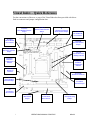
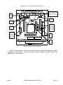
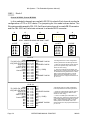
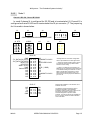
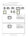
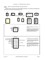
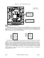
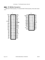
OPERATIONS MANUAL PCM-ESCC NOTE: This manual has been designed and created for use as part of the WinSystems’ Technical Manuals CD and/or the WinSystems’ website. If this manual or any portion of the manual is downloaded, copied or emailed, the links to additional information (i.e. software, cable drawings) will be inoperable. WinSystems reserves the right to make changes in the circuitry and specifications at any time without notice. Copyright 1994 by WinSystems. All Rights Reserved. WinSystems - "The Embedded Systems Authority" REVISION HISTORY P/N 403-0208-000 ECO Number Date Code ORIGINATED 95-08 99-08 941202 950315 990412 Revision B C C1 TABLE OF CONTENTS Section Paragraph Title Visual Index- Quick Reference Page i 1 General Information 1-1 1.1 1.2 1.3 Features General Description Specifications 1-1 1-1 1-3 2 PCM-ESCC Technical Reference 2-1 2.1 2.2 2.3 2.4 2.5 2.6 2.7 2.8 2.9 Introduction I/O Address Selection Serial Mode Selection I/O Address Assignment DMA Configuration Synchronous Mode Options Interrupt Routing PC/104 Bus Connectors Connector/Jumper Summary 2-1 2-1 2-2 2-2 2-13 2-14 2-15 2-16 2-17 APPENDIX Zilog ESCC User's Manual Reprint and Cable Drawings Warranty and Repair Information Visual Index – Quick Reference For the convenience of the user, a copy of the Visual Index has been provided with direct links to connector and jumper configuration data. J2 (CH-A) Clock/RX Data Selection Jumper J4 (CH-A) Clock/TX Data Selection Jumper J5 Channel A/Channel B Mode Selection Jumper J1 (CH-A) RS-422-RS-485 I/O Connector J7 (CH-B) RS-422/RS-485 I/O Connector J6 (CH-B) RX Data Selection Jumper J3 (CH-A) RX Source Selection Jumper J10, J11 Synchronous Clock Routing Selection J9 (CH-A) DTE/DCE Configuration Selection J12 (CH-B) DTE/DCE Configuration Selection J8 (CH-A) RS-232 I/O Connector J14 (CH-B) RS-232 I/O Connector J15 Interrupt/DMA Selection Jumper J13 I/O Address Selection Jumper J17 PC/104 8-bit Bus Connector J19 DMA Enable Jumper i J18 PC/104 16-bit Bus Connector OPERATIONS MANUAL PCM-ESCC J16 Interrupt Routing Jumper 990412 1 GENERAL INFORMATION 1.1 FEATURES n n n n n n n n n 1.2 Two independent, full-duplex serial channels Utilizes Zilog 85230 Enhanced Serial Communications Controller (ESCC) 4 byte transmit FIFO, 8 byte receive FIFO Asynchronous and synchronous protocols RS-232 Interface and RS422/RS485 interface with optional driver chip kit(s) RS-232 configurable as DTE or DCE Jumper Selectable Interrupt routing +5 Volt only operation Supports DMA transfers for Transmit and/or Receive Data GENERAL DESCRIPTION The PCM-ESCC is a PC/104 dual channel, multi-protocol data communications controller based upon the Zilog 85230 ESCC. The module can be configured to satisfy a wide variety of serial communications application needs. Each channel is independent and capable of synchronous or asynchronous data communications with either RS-232 or optional RS-422/RS-485 electrical levels. In synchronous mode, the ESCC can support BISYNC, SDLC, and HDLC including CRC generation, sync character insertion/deletion and many other protocol dependent features. Each chan nel is con fig ur able as Data Ter mi nal Equip ment (DTE) or Data Communications Equipment (DCE). The onboard 85230 in addition to it's asynchronous and synchronous protocol capabilities also sports a 4 byte transmit FIFO and an 8 byte receive FIFO both of which have programmable interrupt or DMA request levels. 990412 OPERATIONS MANUAL PCM-ESCC Page 1-1 WinSystems - "The Embedded Systems Authority" 1.3 SPECIFICATIONS 1.3.1 Electrical Bus Interface : PC/104 8-Bit Optional 16-Bit connector allows access to higher number interrupts. VCC : +5V +/-5% @ 140 mA. I/O Addressing : Uses 4 consecutive I/O addresses, the base of which is jumper selectable from 000H to 3FFH. 1.3.2 Mechanical Dimensions : 3.6 X 3.8 X 0.6 inches PC Board : FR4 Epoxy Glass, with 2 signal layers and 2 power planes with screened component legend and plated through holes. Connectors : 26 Pin 0.10" grid RN type IDH-26-LP for async/sync I/O 10 Pin 0.10" grid RN type IDH-10-LP for RS-422/RS- 485 Jumpers : 1.3.3 0.025" square posts on 0.10" centers Environmental Operating Temperature : -40° to 85° C Non-Condensing relative humidity : 5% to 95% Page 1-2 OPERATIONS MANUAL PCM-ESCC 990412 2 PCM-ESCC Technical Reference 2.1 Introduction This section of the manual is intended to provide the necessary information for the configuration of the PCM-ESCC module to the desired mode of operation. The PCM-ESCC utilizes the very versatile but somewhat complex Zilog 85230 ESCC. The full text of the Zilog SCC user's manual pertaining to the 85230 is reprinted in Appendix C and should be referred to for register and programming details. WinSystems maintains a technical support group to assist in the configuration and usage of this product. Questions not adequately covered in this manual can be addressed to the technical support department at (817) 274-7553 between the hours of 8AM and 5PM Central Time. Alternately assistance can be requested via FAX at (817) 548-1358. 2.2 I/O Address Selection Base I/O Address Select Jumper J13 J13 16 o 14 o 12 o 10 o 8o 6o 4o 2o o o o o o o o o 15 13 11 9 7 5 3 1 A2 A3 A4 A5 A6 A7 A8 A9 The PCM-ESCC uses 4 consecutive I/O addresses beginning at the address specified by the jumpering of J13. A jumper present matches a '0' in the address where a jumper absent matches a '1' in the address. A sample jumpering for I/O address 230H is shown on the following page. 990412 OPERATIONS MANUAL PCM-ESCC Page 2-1 WinSystems - "The Embedded Systems Authority" J13 16 o 14 o 12 o 10 o 8o 6o 4o 2o Sample I/O Select for 230H o o o o o o o o 15 13 11 9 7 5 3 1 A2 A3 A4 A5 A6 A7 A8 A9 I/O Address assignment 2.3 The ESCC uses 4 consecutive addresses which are defined below. The BASE address is set via J13 as defined earlier. Refer to the SCC user's manual reprint in Appendix D for details regarding register and programming values. BASE + 0 = Channel A Data Port BASE + 1 = Channel A Command Port BASE + 2 = Channel B Data Port BASE + 3 = Channel B Command Port Serial Mode Selection 2.4 The extreme versatility of the PCM-ESCC and the 85230 presents an overwhelming challenge in attempting to document all of the possible modes and protocols. In an attempt to simplify the task the following pages will document the proper jumpering for the 9 most commonly used configurations of RS-232, RS-422 and RS-485. Reference to the PCMESCC schematic diagrams in Appendix D can be very helpful in understanding the usage and possible combinations for the serial configuration jumpers. Mode Number 1 2 3 4 5 6 7 8 9 Page 2-2 Channel A Channel B RS-232 RS-232 RS-232 RS-422 RS-422 RS-422 RS-485 RS-485 RS-485 RS-232 RS-422 RS-485 RS-232 RS-422 RS-485 RS-232 RS-422 RS-485 OPERATIONS MANUAL PCM-ESCC 990412 WinSystems - "The Embedded Systems Authority" J5 2 o o 1 J2 3o 2o 1o 4 o o 3 6 o o 5 8 o o 7 10 12 o o o o 9 11 J6 1 2 3 o o o J3 1 2 3 o o o J12 12 o o 11 10 o o 9 8o o7 6o o5 4o o3 2o o1 J4 1 2 3 o o o J9 12 o o 11 10 o o 9 8o o7 6o o5 4o o3 2o o1 J10 3o 2o 1o J11 3o 2o 1o SERIAL CONFIGURATION JUMPERS Choose a mode number that most closely matches the desired usage and jumper according to that section. Variations for synchronous support or DMA use will be addressed in a later section. 990412 OPERATIONS MANUAL PCM-ESCC Page 2-3 WinSystems - "The Embedded Systems Authority" Mode 1 2.4.1 Channel A RS232, Channel B RS232 In this mode both channels are used with RS-232 Line levels. Each channel can also be configured as a DTE or DCE device. The jumpering for this mode is shown below. The Winsystems cable assembly CBL-101-3 will terminate a channel in a male DB-25 connector and the CBL-102-3 will terminate a channel in a female DB-25 connector. J2 3o 2o 1o J4 1 2 3 o o o J3 1 2 3 o o o GRAY JUMPER BLOCKS ARE DON'T CARE J9 DTE 12 o 10 o 8o 6o 4o 2o o 11 o9 o7 o5 o3 o1 J9 DCE 12 o 10 o 8o 6o 4o 2o J10 3o 2o 1o o 11 o9 o7 o5 o3 o1 J11 3o 2o 1o 2 o o 1 4 o o 3 J5 6 8 o o o o 5 7 10 12 o o o o 9 11 J12 DTE 12 o o 11 10 o o 9 8o o7 6o o5 4o o3 2o o1 J6 1 2 3 o o o J12 DCE 12 o o 11 10 o o 9 8o o7 6o o5 4o o3 2o o1 CH A J8 GND *TX_DATA (RX_DATA) *RX_DATA (TX_DATA) *RTS (CTS) *CTS (RTS) *DSR*** (DTR) GND Carrier Detect N/C N/C N/C N/C N/C 1o 2o 3o 4o 5o 6o 7o 8o 9o 10 o 11 o 12 o 13 o o 14 o 15 o 16 o 17 o 18 o 19 o 20 o 21 o 22 o 23 o 24 o 25 o 26 N/C TRANSMIT CLOCK** N/C RECEIVER CLOCK* N/C N/C *DTR (***DSR) N/C N/C N/C TRANSMIT CLOCK** N/C N/C *First Signal shown is for DTE configuration. Label in parenthesis is the DCE signal name. ** These are optional signals typically used for synchronous protocols only. Refer to Later section for clock routing. *** There is no DSR input to the 85230. The DSR input pin is routed to the Carrier detect Pin on the 85230 meaning that assertion on either DSR or Carrier detect will result in a carrier detect presence at the 85230. If this is not desired remove the J9 jumper that attaches to pin 10 on J9 CH B J14 GND *TX_DATA (RX_DATA) *RX_DATA (TX_DATA) *RTS (CTS) *CTS (RTS) *DSR*** (DTR) GND Carrier Detect N/C N/C N/C N/C N/C Page 2-4 1o 2o 3o 4o 5o 6o 7o 8o 9o 10 o 11 o 12 o 13 o o 14 o 15 o 16 o 17 o 18 o 19 o 20 o 21 o 22 o 23 o 24 o 25 o 26 N/C N/C N/C RECEIVER CLOCK* N/C N/C *DTR (***DSR) N/C N/C N/C TRANSMIT CLOCK** N/C N/C *First Signal shown is for DTE configuration. Label in parenthesis is the DCE signal name. ** These are optional signals typically used for synchronous protocols only. Refer to Later section for clock routing. *** There is no DSR input to the 85230. The DSR input pin is routed to the Carrier detect Pin on the 85230 meaning that assertion on either DSR or Carrier detect will result in a carrier detect presence at the 85230. If this is not desired remove the J12 jumper that attaches to pin 3 on J12 OPERATIONS MANUAL PCM-ESCC 990412 WinSystems - "The Embedded Systems Authority" Mode 2 2.4.2 Channel A RS-232, Channel B RS-422 In mode 2 channel A is configured for RS-232 and is terminated at J8. Channel B is configured as 4-wire RS-422 and is terminated at the 10-pin connector J7. The jumpering for this mode is shown below. J2 3o 2o 1o J4 1 2 3 o o o J3 1 2 3 o o o GRAY JUMPER BLOCKS ARE DON'T CARE J9 DTE 12 o 10 o 8o 6o 4o 2o o 11 o9 o7 o5 o3 o1 J9 DCE 12 o 10 o 8o 6o 4o 2o J10 3o 2o 1o o 11 o9 o7 o5 o3 o1 J11 3o 2o 1o 2 o o 1 4 o o 3 J5 6 8 10 12 o o o o o o o o 5 7 9 11 J6 1 2 3 o o o J12 12 o o 11 10 o o 9 8o o7 6o o5 4o o3 2o o1 CH A J8 GND *TX_DATA (RX_DATA) *RX_DATA (TX_DATA) *RTS (CTS) *CTS (RTS) *DSR*** (DTR) GND Carrier Detect N/C N/C N/C N/C N/C 1o 2o 3o 4o 5o 6o 7o 8o 9o 10 o 11 o 12 o 13 o o 14 o 15 o 16 o 17 o 18 o 19 o 20 o 21 o 22 o 23 o 24 o 25 o 26 N/C TRANSMIT CLOCK** N/C RECEIVER CLOCK* N/C N/C *DTR (***DSR) N/C N/C N/C TRANSMIT CLOCK** N/C N/C 990412 1 2 3 4 5 o o o o o o 6 o 7 o 8 o 9 o 10 ** These are optional signals typically used for synchronous protocols only. Refer to Later section for clock routing. *** There is no DSR input to the 85230. The DSR input pin is routed to the Carrier detect Pin on the 85230 meaning that assertion on either DSR or Carrier detect will result in a carrier detect presence at the 85230. If this is not desired remove the J9 jumper that attaches to pin 10 on J9 Requires the installation of 75176 driver ICs in locations U3 and U4 CH B J7 N/C TX+ TXN/C GND *First Signal shown is for DTE configuration. Label in parenthesis is the DCE signal name. RX+ RXN/C N/C +5V The RTS line must be asserted in order to enable the transmitter. User installable termination resistor locations are present on the board at R7 through R12. Refer to the schematic diagrams for specific resistor locations. +5V and ground are also available on the I/O connector in order to allow termination of the cable itself. OPERATIONS MANUAL PCM-ESCC Page 2-5 WinSystems - "The Embedded Systems Authority" Mode 3 2.4.3 Channel A RS-232, Channel B RS-485 Mode 3 sets the A channel as conventional RS-232 in either a DTE or DCE configuration terminated at J8. Channel B is configured for RS-485 multi-drop terminated at J7 The RTS line on channel B controls the transmit/receive function. J2 3o 2o 1o J4 1 2 3 o o o J3 1 2 3 o o o GRAY JUMPER BLOCKS ARE DON'T CARE J9 DTE 12 o 10 o 8o 6o 4o 2o o 11 o9 o7 o5 o3 o1 J9 DCE 12 o 10 o 8o 6o 4o 2o J10 3o 2o 1o o 11 o9 o7 o5 o3 o1 J11 3o 2o 1o 2 o o 1 4 o o 3 J5 6 8 o o o o 5 7 10 12 o o o o 9 11 J6 1 2 3 o o o J12 12 o o 11 10 o o 9 8o o7 6o o5 4o o3 2o o1 CH A J8 GND *TX_DATA (RX_DATA) *RX_DATA (TX_DATA) *RTS (CTS) *CTS (RTS) *DSR*** (DTR) GND Carrier Detect N/C N/C N/C N/C N/C 1o 2o 3o 4o 5o 6o 7o 8o 9o 10 o 11 o 12 o 13 o o 14 o 15 o 16 o 17 o 18 o 19 o 20 o 21 o 22 o 23 o 24 o 25 o 26 N/C TRANSMIT CLOCK** N/C RECEIVER CLOCK* N/C N/C *DTR (***DSR) N/C N/C N/C TRANSMIT CLOCK** N/C N/C CH B J7 N/C TX/RX+ TX/RXN/C GND Page 2-6 1 2 3 4 5 o o o o o o 6 o 7 o 8 o 9 o 10 N/C N/C N/C N/C +5V *First Signal shown is for DTE configuration. Label in parenthesis is the DCE signal name. ** These are optional signals typically used for synchronous protocols only. Refer to Later section for clock routing. *** There is no DSR input to the 85230. The DSR input pin is routed to the Carrier detect Pin on the 85230 meaning that assertion on either DSR or Carrier detect will result in a carrier detect presence at the 85230. If this is not desired remove the J9 jumper that attaches to pin 10 on J9 Requires installation of 75176 driver IC in location U4. The RTS line must be asserted for transmit and disasserted for receive. Resistor locations R10 through R12 are provided on the board for user installable termination resistors. +5V and ground are also available on the I/O connector OPERATIONS MANUAL PCM-ESCC 990412 WinSystems - "The Embedded Systems Authority" Mode 4 Channel A RS-422, Channel B RS-232 2.4.4 Mode number 4 sets up channel A as RS-422 at J1 and Channel B as RS-232 at J14. J2 3o 2o 1o J4 1 2 3 o o o J3 1 2 3 o o o GRAY JUMPER BLOCKS ARE DON'T CARE J9 12 o 10 o 8o 6o 4o 2o J10 3o 2o 1o o 11 o9 o7 o5 o3 o1 J11 3o 2o 1o CH A J1 N/C TX+ TXN/C GND 1 2 3 4 5 o o o o o o 6 o 7 o 8 o 9 o 10 RX+ RXN/C N/C +5V 2 o o 1 4 o o 3 J5 6 8 10 12 o o o o o o o o 5 7 9 11 J12 DTE 12 o o 11 10 o o 9 8o o7 6o o5 4o o3 2o o1 J6 1 2 3 o o o J12 DCE 12 o o 11 10 o o 9 8o o7 6o o5 4o o3 2o o1 Requires installation of 75176 driver ICs in locations U1 and U2. The RTS line must be asserted in order to enable the transmitter. User installable termination resistor locations are present on the board at R1 through R6. Refer to the schematic diagrams for specific resistor locations. +5V and ground are also available on the I/O connector in order to allow termination of the cable itself. CH B J14 GND *TX_DATA (RX_DATA) *RX_DATA (TX_DATA) *RTS (CTS) *CTS (RTS) *DSR*** (DTR) GND Carrier Detect N/C N/C N/C N/C N/C 990412 1o 2o 3o 4o 5o 6o 7o 8o 9o 10 o 11 o 12 o 13 o o 14 o 15 o 16 o 17 o 18 o 19 o 20 o 21 o 22 o 23 o 24 o 25 o 26 N/C N/C N/C RECEIVER CLOCK* N/C N/C *DTR (***DSR) N/C N/C N/C TRANSMIT CLOCK** N/C N/C *First Signal shown is for DTE configuration. Label in parenthesis is the DCE signal name. ** These are optional signals typically used for synchronous protocols only. Refer to Later section for clock routing. *** There is no DSR input to the 85230. The DSR input pin is routed to the Carrier detect Pin on the 85230 meaning that assertion on either DSR or Carrier detect will result in a carrier detect presence at the 85230. If this is not desired remove the J12 jumper that attaches to pin 3 on J12 OPERATIONS MANUAL PCM-ESCC Page 2-7 WinSystems - "The Embedded Systems Authority" Mode 5 Channel A RS-422, Channel B RS-422 2.4.5 This mode sets both the A channel at J1 and the B channel at J7 to RS-422. J2 3o 2o 1o J4 1 2 3 o o o J3 1 2 3 o o o GRAY JUMPER BLOCKS ARE DON'T CARE J9 12 o 10 o 8o 6o 4o 2o J10 3o 2o 1o o 11 o9 o7 o5 o3 o1 CH A J1 N/C TX+ TXN/C GND 1 2 3 4 5 o o o o o o 6 o 7 o 8 o 9 o 10 RX+ RXN/C N/C +5V CH B J7 N/C TX+ TXN/C GND Page 2-8 1 2 3 4 5 o o o o o o 6 o 7 o 8 o 9 o 10 RX+ RXN/C N/C +5V 2 o o 1 4 o o 3 10 12 o o o o 9 11 J6 1 2 3 o o o J12 J11 3o 2o 1o J5 6 8 o o o o 5 7 12 o 10 o 8o 6o 4o 2o o 11 o9 o7 o5 o3 o1 Requires installation of 75176 driver ICs in locations U1 and U2. The RTS line must be asserted in order to enable the transmitter. User installable termination resistor locations are present on the board at R1 through R6. Refer to the schematic diagrams for specific resistor locations. +5V and ground are also available on the I/O connector in order to allow termination of the cable itself. Requires the installation of 75176 driver ICs in locations U3 and U4. The RTS line must be asserted in order to enable the transmitter. User installable termination resistor locations are present on the board at R7 through R12. Refer to the schematic diagrams for specific resistor locations. +5V and ground are also available on the I/O connector in order to allow termination of the cable itself. OPERATIONS MANUAL PCM-ESCC 990412 WinSystems - "The Embedded Systems Authority" Mode 6 Channel A RS-422, Channel B RS-485 2.4.6 Mode 6 sets channel A as RS-422 terminated at J1 and sets Channel B as RS-485 terminated at J7. J2 3o 2o 1o J4 1 2 3 o o o J3 1 2 3 o o o GRAY JUMPER BLOCKS ARE DON'T CARE J9 12 o 10 o 8o 6o 4o 2o J10 3o 2o 1o o 11 o9 o7 o5 o3 o1 CH A J1 N/C TX+ TXN/C GND 1 2 3 4 5 o o o o o o 6 o 7 o 8 o 9 o 10 RX+ RXN/C N/C +5V 2 o o 1 4 o o 3 10 12 o o o o 9 11 J6 1 2 3 o o o J12 J11 3o 2o 1o J5 6 8 o o o o 5 7 12 o 10 o 8o 6o 4o 2o o 11 o9 o7 o5 o3 o1 Requires installation of 75176 driver ICs in locations U1 and U2. The RTS line must be asserted in order to enable the transmitter. User installable termination resistor locations are present on the board at R1 through R6. Refer to the schematic diagrams for specific resistor locations. +5V and ground are also available on the I/O connector in order to allow termination of the cable itself. CH B J7 N/C TX/RX+ TX/RXN/C GND 990412 1 2 3 4 5 o o o o o o 6 o 7 o 8 o 9 o 10 N/C N/C N/C N/C +5V Requires the installation of 75176 driver IC in location U4. The RTS line must be asserted for transmit and disasserted for receive. Resistor locations R10 through R12 are provided on the board for user installable termination resistors. +5V and ground are also available on the I/O connector to allow termination of the cable itself. OPERATIONS MANUAL PCM-ESCC Page 2-9 WinSystems - "The Embedded Systems Authority" Mode 7 Channel A RS-485, Channel B RS-232 2.4.7 Mode number 7 sets channel A as RS-485 terminated at J1. Channel B is configured for either DTE or DCE and is terminated at J14. J2 3o 2o 1o J4 1 2 3 o o o J3 1 2 3 o o o GRAY JUMPER BLOCKS ARE DON'T CARE J9 12 o 10 o 8o 6o 4o 2o J10 3o 2o 1o o 11 o9 o7 o5 o3 o1 J11 3o 2o 1o CH A J1 N/C TX/RX+ TX/RXN/C GND 1 2 3 4 5 o o o o o o 6 o 7 o 8 o 9 o 10 N/C N/C N/C N/C +5V 2 o o 1 4 o o 3 J5 6 8 o o o o 5 7 10 12 o o o o 9 11 J12 DTE 12 o o 11 10 o o 9 8o o7 6o o5 4o o3 2o o1 J6 1 2 3 o o o J12 DCE 12 o o 11 10 o o 9 8o o7 6o o5 4o o3 2o o1 Requires the installation of 75176 driver IC in location U2. The RTS line must be asserted for transmit and disasserted for receive. Resistor locations R4 through R6 are provided on the board for user installable termination resistors. +5V and ground are also available on the I/O connector to allow termination of the cable itself. CH B J14 GND *TX_DATA (RX_DATA) *RX_DATA (TX_DATA) *RTS (CTS) *CTS (RTS) *DSR*** (DTR) GND Carrier Detect N/C N/C N/C N/C N/C Page 2-10 1o 2o 3o 4o 5o 6o 7o 8o 9o 10 o 11 o 12 o 13 o o 14 o 15 o 16 o 17 o 18 o 19 o 20 o 21 o 22 o 23 o 24 o 25 o 26 N/C N/C N/C RECEIVER CLOCK* N/C N/C *DTR (***DSR) N/C N/C N/C TRANSMIT CLOCK** N/C N/C *First Signal shown is for DTE configuration. Label in parenthesis is the DCE signal name. ** These are optional signals typically used for synchronous protocols only. Refer to Later section for clock routing. *** There is no DSR input to the 85230. The DSR input pin is routed to the Carrier detect Pin on the 85230 meaning that assertion on either DSR or Carrier detect will result in a carrier detect presence at the 85230. If this is not desired remove the J12 jumper that attaches to pin 3 on J12 OPERATIONS MANUAL PCM-ESCC 990412 WinSystems - "The Embedded Systems Authority" Mode 8 Channel A RS-485, Channel B RS-422 2.4.8 Mode 8 sets Channel A to terminate at J1 for RS-485, it also sets channel B for RS-422 terminated at J7. J2 3o 2o 1o J4 1 2 3 o o o J3 1 2 3 o o o GRAY JUMPER BLOCKS ARE DON'T CARE J9 12 o 10 o 8o 6o 4o 2o J10 3o 2o 1o o 11 o9 o7 o5 o3 o1 CH A J1 N/C TX/RX+ TX/RXN/C GND 1 2 3 4 5 o o o o o o 6 o 7 o 8 o 9 o 10 N/C N/C N/C N/C +5V CH B J7 N/C TX+ TXN/C GND 990412 1 2 3 4 5 o o o o o o 6 o 7 o 8 o 9 o 10 J11 3o 2o 1o 2 o o 1 4 o o 3 J5 6 8 o o o o 5 7 10 12 o o o o 9 11 J6 1 2 3 o o o J12 12 o o 11 10 o o 9 8o o7 6o o5 4o o3 2o o1 Requires installation of 75176 driver IC in location U2. The RTS line must be asserted for transmit and disasserted for receive. Resistor locations R4 through R6 are provided on the board for user installable termination resistors. +5V and ground are also available on the I/O connector to allow termination of the cable itself. Requires installation of 75176 driver ICs in locations U3 and U4. RX+ RXN/C N/C +5V The RTS line must be asserted in order to enable the transmitter. User installable termination resistor locations are present on the board at R7 through R12. Refer to the schematic diagrams for specific resistor locations. +5V and ground are also available on the I/O connector in order to allow termination of the cable itself. OPERATIONS MANUAL PCM-ESCC Page 2-11 WinSystems - "The Embedded Systems Authority" Mode 9 Channel A RS-485, Channel B RS-485 2.4.9 In mode 9 both channels A and B are set for RS-485 and terminated at J1 and J7 respectively. J2 3o 2o 1o J4 1 2 3 o o o J3 1 2 3 o o o GRAY JUMPER BLOCKS ARE DON'T CARE J9 12 o 10 o 8o 6o 4o 2o J10 3o 2o 1o o 11 o9 o7 o5 o3 o1 CH A J1 N/C TX/RX+ TX/RXN/C GND 1 2 3 4 5 o o o o o o 6 o 7 o 8 o 9 o 10 N/C N/C N/C N/C +5V CH B J7 N/C TX/RX+ TX/RXN/C GND Page 2-12 1 2 3 4 5 o o o o o o 6 o 7 o 8 o 9 o 10 N/C N/C N/C N/C +5V J11 3o 2o 1o 2 o o 1 4 o o 3 J5 6 8 o o o o 5 7 10 12 o o o o 9 11 J6 1 2 3 o o o J12 12 o o 11 10 o o 9 8o o7 6o o5 4o o3 2o o1 Requires installation of 75176 driver IC in location U2. The RTS line must be asserted for transmit and disasserted for receive. Resistor locations R4 through R6 are provided on the board for user installable termination resistors. +5V and ground are also available on the I/O connector to allow termination of the cable itself. Requires installation of 75176 driver IC in location U4. The RTS line must be asserted for transmit and disasserted for receive. Resistor locations R10 through R12 are provided on the board for user installable termination resistors. +5V and ground are also available on the I/O connector to allow termination of the cable itself. OPERATIONS MANUAL PCM-ESCC 990412 WinSystems - "The Embedded Systems Authority" DMA Configuration jumpers J19 and J16. J16 2 o o 1 4 o o 3 6 o o 5 8 o o 7 10 12 14 16 o o o o o o o o 9 11 13 15 J19 1 2 3 4 o o o o DMA Configuration 2.5 The PCM-ESCC and the Zilog 85230 can be configured for DMA data transfers using DMA channels 1 and 3 on the PC/104 bus. The jumper block at J19 and the top two pins of J16 are used to configure the DMA channel routing. Refer to the reprint of the ESCC user's manual for programming details. The supported DMA options are shown below. J16 2 o o 1 4 o o 3 6 o o 5 8 o o 7 J16 10 12 14 16 o o o o o o o o 9 11 13 15 J19 1 2 3 4 o o o o 2 o o 1 4 o o 3 6 o o 5 J16 4 o o 3 6 o o 5 8 o o 7 10 12 14 16 o o o o o o o o 9 11 13 15 J19 1 2 3 4 o o o o J16 J19 1 2 3 4 o o o o Channel B RX DMA - DRQ1 Channel B TX DMA - DRQ3 990412 10 12 14 16 o o o o o o o o 9 11 13 15 Channel A RX DMA - DRQ1 Channel A TX DMA - DRQ3 DMA DISABLED 2 o o 1 8 o o 7 2 o o 1 4 o o 3 6 o o 5 8 o o 7 10 12 14 16 o o o o o o o o 9 11 13 15 J19 1 2 3 4 o o o o Channel A TX/RX DMA - DRQ1 Channel B TX/RX DMA - DRQ3 OPERATIONS MANUAL PCM-ESCC Page 2-13 WinSystems - "The Embedded Systems Authority" Synchronous Mode Options 2.6 J2 J4 3o 2o 1o 3 2 1 o o o J10 3 o 2 o 1 o J11 3 o 2 o 1 o Clock routing jumpers J2, J4, J10, J11 When programmed for synchronous modes it is often necessary to provide or recognize the Transmit/Receive Clock(s) from/to the I/O device. There are several routing jumpers available to provide maximum flexibility in clock routing. The clock routing jumpers are shown below. /RTXCA CH A J8 Pin 17 /TRXCA CHA J8 Pin 24 J10 3o 2o 1o 3o 2o 1o J11 CHA J8 Pin 15 CHB J14 Pin /RTXCB + J2 3o 2o 1o CHA J1 Pin 6 CHA J1 Pin 7 - RXA2 /TRXCB CHB J14 Pin 24 + J4 TXDA Page 2-14 CHA J1 Pin 2 3o 2o 1o - OPERATIONS MANUAL PCM-ESCC CHA J1 Pin 3 990412 WinSystems - "The Embedded Systems Authority" Interrupt Select Jumpers J15, J16 J15 2 o o 1 4 o o 3 6 o o 5 8 o o 7 10 o o 9 12 14 o o o o 11 13 J16 2 o o 1 2.7 4 o o 3 6 o o 5 8 10 12 14 16 o o o o o o o o o o 7 9 11 13 15 Interrupt Routing The 85230 interrupt can be routed to any free PC/104 Bus interrupt using J16. If the optional PCM-ESCC-16 board is used there are additional interrupt choices available by selecting via J15. J15 also provides support for interrupt sharing. The diagrams below detail the interrupt routing and sharing jumpers. IRQ7 IRQ6 IRQ5 IRQ4 IRQ3 IRQ2 J16 1 o o 3 o o 5 o o 7 o o 9 o o 11 o o 13 o o 15 o o 2 4 6 8 10 12 14 16 IRQ10 IRQ11 IRQ12 IRQ15 IRQ14 J15 1 o o 3 o o 5 o o 7 o o 9 o o 11 o o 13 o o 2 4 6 8 10 12 14 The PCM-ESCC is also capable of sharing a bus interrupt with another PCM-ESCC module or another PC/104 module supporting interrupt sharing. Either the base CPU board or one of the modules sharing the interrupt must terminate the interrupt with a pulldown resistor. WinSystems CPU boards do NOT provide this pulldown so it must be enabled at the PC/104 module. To enable interrupt sharing remove the factory installed jumper at J15 pins 13-14 and place it on J15 pins 11-12. For non-shared interrupts a jumper should always be in place at J15 pins 13-14. The pulldown resistor is connected by jumpering J15 pins 11-12. 990412 OPERATIONS MANUAL PCM-ESCC Page 2-15 WinSystems - "The Embedded Systems Authority" PC/104 Bus Connectors 2.8 The 8-bit PC/104 connector J17 and the 16-Bit PC/104 connector J18 are both shown here: J17 IOCHK SD7 SD6 SD5 SD4 SD3 SD2 SD1 SD0 IOCHRDY AEN SA19 SA18 SA17 SA16 SA15 SA14 SA13 SA12 SA11 SA10 SA9 SA8 SA7 SA6 SA5 SA4 SA3 SA2 SA1 SA0 GND Page 2-16 A1 o A2 o A3 o A4 o A5 o A6 o A7 o A8 o A9 o A10 o A11 o A12 o A13 o A14 o A15 o A16 o A17 o A18 o A19 o A20 o A21 o A22 o A23 o A24 o A25 o A26 o A27 o A28 o A29 o A30 o A31 o A32 o J18 o o o o o o o o o o o o o o o o o o o o o o o o o o o o o o o o B1 B2 B3 B4 B5 B6 B7 B8 B9 B10 B11 B12 B13 B14 B15 B16 B17 B18 B19 B20 B21 B22 B23 B24 B25 B26 B27 B28 B29 B30 B31 B32 GND RESET +5V IRQ2 -5V DRQ2 -12V 0WS +12V GND SMEMW SMEMR IOW IOR DACK3 DRQ3 DACK1 DRQ1 DACK0 CLK IRQ7 IRQ6 IRQ5 IRQ4 IRQ3 DACK2 T/C BALE +5V OSC GND GND GND MEMCS16 IOCS16 IRQ10 IRQ11 IRQ12 IRQ15 IRQ14 DACK0 DRQ0 DACK5 DRQ5 DACK6 DRQ6 DACK7 DRQ7 +5V MASTER GND GND OPERATIONS MANUAL PCM-ESCC D0 o D1 o D2 o D3 o D4 o D5 o D6 o D7 o D8 o D9 o D10 o D11 o D12 o D13 o D14 o D15 o D16 o D17 o D18 o D19 o o o o o o o o o o o o o o o o o o o o o C0 C1 C2 C3 C4 C5 C6 C7 C8 C9 C10 C11 C12 C13 C14 C15 C16 C17 C18 C19 GND SBHE LA23 LA22 LA21 LA20 LA19 LA18 LA17 MEMR MEMW SD8 SD9 SD10 SD11 SD12 SD13 SD14 SD15 KEY 990412 WinSystems - "The Embedded Systems Authority" 2.9 Connector/Jumper Summary Connector/ Jumper Description Page Reference J1 J2 J3 J4 J5 J6 J7 J8 J9 J10 J11 J12 J13 J14 J15 J16 J17 J18 J19 CH A RS-422/RS-485 I/O connector CH A Clock/RX Data Select Jumper CH A RX source select jumper CH A Clock/TX Data Select Jumper CHA/CHB Mode Select Jumper CH B RX Data select jumper CH B RS-422/RS-485 I/O Connector CH A RS-232 I/O Connector CH A DTE/DCE configuration select Synchronous Clock routing select Synchronous Clock routing select CH B DTE/DCE configuration select I/O Address Select jumper CH B RS-232 I/O Connector Interrupt/DMA Select jumper Interrupt routing jumper PC/104 8-Bit bus connector PC/104 16-Bit bus connector DMA Enable jumper 2-7 2-3 2-3 2-3 2-3 2-3 2-5 2-4 2-3 2-3 2-3 2-3 2-1 2-4 2-15 2-15 2-16 2-16 2-13 990412 OPERATIONS MANUAL PCM-ESCC Page 2-17 APPENDIX A Zilog's ESCC User's Manual Reprint ESCC.ZIP APPENDIX Zilog ESCC User's Manual Reprint Zilog's ESCC User's Manual User Manual Errata scc_escc_um.pdf scc_up0026.pdf Cable Drawings Part Number Description CBL-101-3 26-pin ribbon to 25-pin male "D" connector adapter CBL-102-3 25-pin ribbon to 25-pin female "D" connector adapter Telephone: 817-274-7553 . . Fax: 817-548-1358 http://www.winsystems.com . . E-mail: [email protected] WARRANTY WinSystems warrants that for a period of two (2) years from the date of shipment any Products and Software purchased or licensed hereunder which have been developed or manufactured by WinSystems shall be free of any material defects and shall perform substantially in accordance with WinSystems' specifications therefore. With respect to any Products or Software purchased or licensed hereunder which have been developed or manufactured by others, WinSystems shall transfer and assign to Customer any warranty of such manufacturer or developer held by WinSystems, provided that the warranty, if any, may be assigned. The sole obligation of WinSystems for any breach of warranty contained herein shall be, at its option, either (i) to repair or replace at its expense any materially defective Products or Software, or (ii) to take back such Products and Software and refund the Customer the purchase price and any license fees paid for the same. Customer shall pay all freight, duty, broker's fees, insurance changes and other fees and charges for the return of any Products or Software to WinSystems under this warranty. WinSystems shall pay freight and insurance charges for any repaired or replaced Products or Software thereafter delivered to Customer within the United States. All fees and costs for shipment outside of the United States shall be paid by Customer. The foregoing warranty shall not apply to any Products or Software which have been subject to abuse, misuse, vandalism, accidents, alteration, neglect, unauthorized repair or improper installations. THERE ARE NO WARRANTIES BY WINSYSTEMS EXCEPT AS STATED HEREIN. THERE ARE NO OTHER WARRANTIES EXPRESS OR IMPLIED INCLUDING, BUT NOT LIMITED TO, THE IMPLIED WARRANTIES OF MERCHANTABILITY AND FITNESS FOR A PARTICULAR PURPOSE, IN NO EVENT SHALL WINSYSTEMS BE LIABLE FOR CONSEQUENTIAL, INCIDENTAL, OR SPECIAL DAMAGES INCLUDING, BUT NOT LIMITED TO, DAMAGES FOR LOSS OF DATA, PROFITS OR GOODWILL. WINSYSTEMS' MAXIMUM LIABILITY FOR ANY BREACH OF THIS AGREEMENT OR OTHER CLAIM RELATED TO ANY PRODUCTS, SOFTWARE, OR THE SUBJECT MATTER HEREOF, SHALL NOT EXCEED THE PURCHASE PRICE OR LICENSE FEE PAID BY CUSTOMER TO WINSYSTEMS FOR THE PRODUCTS OR SOFTWARE OR PORTION THEREOF TO WHICH SUCH BREACH OR CLAIM PERTAINS. WARRANTY SERVICE All products returned to WinSystems must be assigned a Return Material Authorization (RMA) number. To obtain this number, please call or FAX WinSystems' factory in Arlington, Texas and provide the following information: 1. Description and quantity of the product(s) to be returned including its serial number. 2. Reason for the return. 3. Invoice number and date of purchase (if available), and original purchase order number. 4. Name, address, telephone and FAX number of the person making the request. 5. Do not debit WinSystems for the repair. WinSystems does not authorize debits. After the RMA number is issued, please return the products promptly. Make sure the RMA number is visible on the outside of the shipping package. The customer must send the product freight prepaid and insured. The product must be enclosed in an anti-static bag to protect it from damage caused by static electricity. Each bag must be completely sealed. Packing material must separate each unit returned and placed as a cushion between the unit(s) and the sides and top of the shipping container. WinSystems is not responsible for any damage to the product due to inadequate packaging or static electricity.