1
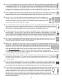
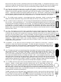
Pocket Tracker
Assembly Instructions version 1.05
These instructions will aid in the assembly of the Pocket Tracker, which is designed to fit perfectly with its 9-volt battery in an
®
Altoids candy tin. A complete Owner’s Manual, which includes this Information, plus pictures and further instructions, will
soon be available at http://www.byonics.com/pockettracker. The zip file also contains the TinyTrak3Config program which
is needed to set user options.
Printed Circuit Board
Parts List
PCA
L10
L7
L1, L2, L4
L5, L6
Pocket Tracker Printed Circuit
Black 26 ga. half turn wire loop, 5 nH
0.12 µH axial leaded inductor
3.3 µH axial leaded inductors
C16
C22
C23
C15
D8
J13
L3
SP1
L8
C33
L11
L12
C32, C34
L9
L13
X1
J8
22 nF capacitor(blue box)
1 nF capacitor (smallest blue box)
100 nF capacitor (blue box)
470 nF capacitor (biggest blue box)
Reverse protection diode
2-pin header
Variable inductor, blue, 6.5 turns
Shield Plate
3.3 µH axial leaded inductor
47 pF ceramic capacitor (brown)
65 nH, 3 turns, 3/16” I. D. 20 ga.
73 nH, 3 turns, 13/64” I. D. 20 ga.
30 pF ceramic (brown)
0.1 µH axial leaded inductor
0.22 µH axial leaded inductor
8.000 MHz Crystal
Serial Port connector, 3/32”,
3-conductor
2-pin headers
+5 Loop
Fuse (not included – see text)
3 header pins
10 MHz ceramic resonator
18-pin DIP socket
3-pin header
Battery clip
TinyTrak or WxTrak PIC
BNC connector
Jumper-Shunts with integrated
handles
Antenna & Battery (not included)
J4, JS
W1
F1
J9
Y1
UX1
J11
J10
U1
J12
JS1, JS2,
JS3
Assembly Instructions
The Pocket Tracker is a moderately simple construction project that can usually be completed in just a few hours. You will
need a low wattage pencil-type soldering iron with a small tip, some thin electronics-grade solder, wire strippers, a ruler, a
3/16” drill bit, a 13/64” drill bit, and a pair of diagonal cutters. Some of the components in the kit are static sensitive, so use
standard precautions. All components are loaded on the white silk-screened side, and then the leads are soldered from the
CIRCUIT side of the board (labeled near one of the square corners). Be sure to solder only the correct pad, and do not let
any solder touch any other pad or trace. Trim away excess leads with diagonal cutters after soldering each component.
Nothing should project below the bottom of the board more than a tenth of an inch. Only a few components must be installed
in a particular orientation: D8, the RF shield, the DIP socket, U1, and the battery clip leads. The checklist below will help
ensure all components are properly assembled.
Before beginning, consider how the Pocket Tracker will be mounted. It may be advantageous to use the PC Assembly as a
template BEFORE soldering on any more components. See the Owner’s Manual for details. Some components on the PC
Assembly are static sensitive, so use standard precautions.
Six backside wires - To enable all features, six 26 gauge wires (supplied) must be added to the back of the board. The board
is shipped with a yellow wire and a blue wire attached to U6 pins 6 and 7 respectively. Guidelines in the solder-mask show
how to route the backside wires. It is not necessary to precisely follow the guidelines. Generally following the guidelines will
keep the wires away from areas where the wires might get pinched in the mounting hardware, keeps the wires away from
adjustment access points, and ensures proper spacing and shielding from sensitive RF circuitry. Route a wire, cut it to
length, strip the ends, and then solder the wire in place from the top of the board. Save the cut off pieces for use later in this
project. Temporarily bend these wires out of the way as needed when soldering in other wires and components.
Blue backside wire (1.556”) - Route the blue wire attached to U6 pin 7 (shown as one of the two dark lines in the circuit
side diagram) along the guideline leading towards the lower left corner of the board. The free end of the blue wire will
be soldered in the pad marked “FS” (Frequency Select) on the bottom of the board. There is a “4” next to this pad on
the top of the board. Cut the 26 ga. blue wire to length, strip the end, and solder the wire from the top (silk-screened)
side of the board. Retain the cut off piece of wire for use later in this project.
Yellow backside wire (2.3”) - Notice that the pad with the yellow wire (shown in gray in the circuit side diagram)
soldered in it has a silver dash above and below the pad. Following the guideline in the solder-mask will lead to
another pad with a silver dash on the left and right sides. Route the yellow wire along the guideline, cut it to length,
strip it, and solder it in the pad bracketed by the two silver dashes. On the top of the board the pad for the yellow wire
will have the letters “RF” with an arrow pointing at it.
Short yellow backside wire (1.175”) – The other yellow backside wire (shown in gray in the diagram) runs roughly
horizontally from the pad adjacent to the left red wire pad (the red wire pads are marked with a nearby “+” sign that has
a hollow center) to a small pad that has a white “T” next to it on the component side of the board.
Short white backside wire (0.75”) - A short white wire runs in a straight line diagonally from the pad closest to the body
of L8 to another pad between the pair of pads used for L9. Follow the guideline in the solder-mask.
Long white backside wire (2.514”) - The pads at each end of this wire are surrounded by a circle in a square. These
pads are not too far from the ends of the long yellow wire. On the top of the board both of these pads are “D” shaped.
One pad is near U6 (outside of the C15 rectangle) and the other pad is between the “L4” and “L8” labels.
Red backside wire, 26 ga. (the thinner of the two red wires supplied in the kit, 3.124” long) – The other long black line
in the diagram represents the red backside wire. The pads at both ends of this wire have a silver “+” sign with a hollow
center nearby. Follow the guideline. The red wire will run between the blue and yellow wires attached to U6. On the
top side of the board, one end of the red wire will be soldered to a pad between the text “J9” and “ON”. The other end
of the red wire gets soldered to a pad labeled “+V” on the top of the board. This pad is near the lower left corner of the
board (as viewed in the component loading diagram), which is the rounded corner without the ground plane and large
mounting-screw hole.
L10 - It works best to install the parts in the order shown on the parts list (top to bottom), basically starting in the center
of the board (with a couple of early exceptions) and working towards the edges. L10 is a “half-turn” five nanoHenry inductor made from a 5/8” piece of 26 ga. black wire that gets routed between the emitter pad of Q5 and
ground. Strip both ends of the wire so that a 5/16” section of insulation remains in the middle. Fold this wire
into a “U” and install it in the two pads: one pad is below the “L” of “L10” in the diagram (on the board the “L” of “L10”
may be partially covered by transistor Q5) and the other pad is in the ground plane just to the right of the “0” in “L10”.
After soldering, fold L10 over towards the L9 pads so the insulated section of the L10 wire touches the ground plane.
L7 (labeled “.12 µH” in the fine print on the side) is the only axial leaded component that is loaded parallel to the
surface of the board. Fold the leads to fit between the pads. The center-to-center spacing is 0.4”. One end
of L7 goes in the pad just above the “L7” text. This pad has a white circle around it. The other lead of L7 is
soldered to the pad that is just below the “L5” text. There is a white semi-circle around this pad. Ignore the bracket
outlines and other pad designed to accommodate a hand-wound coil. Trim the leads after soldering.
2
L1, L2, L4, L5, L6 (labeled “3.3 µH” in the fine print on the side) - All of the remaining axial leaded inductors are
installed upright, with the body perpendicular to the board. It is important that the inductor body go over the pad
surrounded with a white circle. These inductors need to have one lead folded with two 90 degree bends to form
a squared-off inverted “U” with the component body in one of the vertical uprights of the “U”. In some places it
is important that the folded over lead is spaced away from the component body. Form the leads to match the pad
spacing. The exact center-to-center lead spacing is: L1 = 0.178”, L2 = 0.217”, L4, L5, and L6 = 0.1”.
C16 is a medium-sized blue rectangular capacitor with “22n” printed on one side. Either lead can go in either
hole for all kit capacitors. Space the capacitor off the board just enough to clear the surface-mount components
loaded underneath. Ensure C16 is mounted approximately square to the board so that L3 will fit later.
C22, C23, C15 - C22 is the smallest of the blue rectangular capacitors and is marked “1n” on
the side. Space C22 and C23 up off the board just enough to clear the surface-mount
components underneath. C23 is the smaller of the two remaining blue rectangular capacitors.
C15, the largest blue rectangular capacitor, is marked “470n” on the top. Since C15 is a very
tall part, take care to install C15 flush with the board.
D8 is installed between C22, C23, and the edge of the board. The cathode lead (banded end) of D8 must be
connected to the square pad. Folding the cathode lead into a “U” that is just barely taller than C23, but not taller
than C15 so it can’t short to the lid or rim of the can, makes a convenient place to check the voltage on the input
of the regulator. Position the body of D8 over the round pad that is surrounded by a white circle.
J13: Snap two pins off the end of the 12-pin header strip supplied in the kit. Solder these pins in the two pads
next to the white “T” to the left of L4. These pads are nearly surrounded by a white rectangle. Use a jumpershunt (3 supplied) as a handle to hold the pin-pair while soldering. Space the pins up off the board just enough to
clear the surface-mount components underneath. Be sure to remove the jumper-shunt after soldering the pins in
place to avoid the risk of damaging the jumper-shunt while installing other nearby components like the shield plate.
L3 is a 6.5 turn variable inductor wound on a dark blue plastic frame that is about 3/8” square by ½” tall. The
two L3 pads are on opposite corners of the big white square on the component side of the board. Since L3 is
a fairly tall component, take care to mount L3 flush to the board.
Shield Plate - The edge of the shield plate is shown as a long thin line in the loading diagram between L12 and C33.
The top corner notch will line up with the edge of the board and the shield plate will extend nearly all
the way to L3. Make certain that the bottom edge of the shield does not short to the trace that runs
between the legs of the shield. The shield should not touch the +5 volt power plane under the end
of the shield near “L3”. Solder tack the legs of the shield in place. Once confident in the position,
solder four full-length fillets (two on each side) along the bottom edge of the shield where it
contacts the exposed ground plane sections. The legs are merely assembly aids and do not provide
a sufficient ground connection for effective shielding. After soldering the fillets, completely fill the holes around the
shield legs with solder and trim off any excess length.
L8 (labeled “3.3 µH” in the fine print on the side) – Fold over one lead of L8 to form a “U” with the body of the
component in one of the uprights. The center-to-center spacing between the leads will be 0.214”. The body of
the inductor will be installed in the pad with a white circle around it, just above the “L8” text. A white line leads
to the other L8 pad.
C33 is one of the three brown capacitors. “47 ± 5%” is printed on one side of C33. Install this capacitor right
next to the shield. One lead goes in a pad that’s in the middle of a wide trace that extends under the shield
and the other lead gets soldered to a hole in the ground plane that extends to the edge of the board. Solder
the capacitor just high enough above the board to allow for good solder fillets around the pads and leads.
L11 is made from a 2.6” long piece of 20 gauge enamel coated red magnet-wire (supplied). Wind the wire around the
shank of a 3/16” drill bit for three complete turns (winding direction does not matter), then bend the
ends out perpendicular to the coil along a common radial. End and side views of L11 looks like the
drawing (shown about 1.5 times actual size). Use a hobby knife to scrape the enamel completely off
both legs of the coil for about 9/64”, then solder both leads of the coil to the pads. Keep
the leads short, but space the coil up off the board just enough to get good solder fillets and to ensure
that the coil can’t short to the nearby ground planes. Install L11 next to C33. L11 connects C32 to C33. L11 does not
connect to the ground plane.
3
L12 is exactly like L11 except it is wound around the shank of a 13/64” drill bit. Install L12 just like L11, except on the
opposite side of the shield from C33. Just make sure L12 does not short out to the shield. The enamel should provide
adequate insulation.
C32 and C34 are both brown capacitors with “30 ± 5%” printed on one side. Solder these capacitors into their
respective locations as shown in the silk-screen on the PC board, parallel to C33. Again, keep these
capacitors as close to the PC board as possible, allowing just enough space to get good solder fillets between
the pads and the leads on the top and bottom sides of the board.
L9 (labeled “.10 µH” in the fine print on the side) – Fold over one lead of L9 to form a “U” with the body of the
component in one of the uprights. The center-to-center spacing between the leads will be 0.153”. The body of
the inductor will be installed in the pad with a white circle around it, just below the “L9” text. A white line leads
to the other L9 pad.
L13 (labeled “.22 µH” in the fine print on the side) – Fold over one lead of L13 to form a “U” with the body of the
component in one of the uprights. It’s OK if the folded over lead of L13 touches the body of the inductor. The
center-to-center spacing between the leads will be 0.074”. L13 is installed next to the antenna connector notch
between C34 and the edge of the board. Install the body of L13 above the pad nearly surrounded by the white
circle. The other lead is soldered in a hole in the ground plane right next to the outline for C34.
X1 (labeled “8.00” on one side) – Install the crystal spaced just above the board so that the case of the crystal
cannot short the traces and pads underneath to the surrounding ground plane. Either lead can go in either pad.
The crystal is another tall component, so keep the body as closed to the board without touching as possible.
J8 – A text line near the crystal says “© 2004 HiValue Radio”. Next to the word “Value” there is a white rectangle with
two round pads in it. One of the pads has a white circle around it. Cut a yellow 26 ga. wire 1.75” long.
Strip each end 3/16”. Solder one end in the pad with the white circle around it. Cut a blue 26 ga. wire 1.5”
long. Strip each end 3/16”. Solder one end to the other pad within the white rectangle. Cut a black 26 ga.
wire 1.75” long. Strip each end 3/16”. Solder one end in the square pad near the “4” and the “H” of the text
line near the crystal. Twist these three wires together. These wires will be soldered to the Serial Port connector as
one of the last steps in the assembly process.
J4 and JS – Referring again to the text line near the crystal, J4 is a 2-pin header that mounts near the copyright
symbol © in this line of text. There is a square pad and a round pad with adjacent white squares around these
two pads. A jumper-shunt can temporarily be placed over the two pins and used as a handle while soldering.
Placing a jumper-shunt on these two pins enables the LEDs. Moving down two rows of pads towards the small
notch in the edge of the board there is a pair of round pads surrounded by a white rectangle. Another 2-pin header
(JS for Jumper Storage) can be mounted in this location to provide a place to store the LED jumper when it’s not in
use. Note that these two pins will be connected to the regulated +5 volts supply, so these pins make a convenient test
point. Take care not to short these points to any other circuit nodes.
W1 – Within the outline for U2 there are three round pads. One of these pads has a white line next to it that
extends towards the round anode pad for D7. Placing a jumper wire from one end of this white line to the other
provides a way for the TinyTrak circuitry to get regulated +5 volts from the Pocket Tracker transmitter. A piece of
cut off component lead can be folded into a “U” and soldered between these two pads. If the wire loop is made high
enough to extend above neighboring components, but not so high that it will short out against the lid, this wire loop
can make a convenient +5 volt test point. The center-to-center distance between the two pads is 0.106”. Starting with
a piece of wire that is 1.3” long works about right. Insert the loop to the desired depth, solder in place, then cut off any
excess.
F1 – Pads on the board can be used to mount a through-hole or surface-mount “pico-fuse” (neither provided) that is
in series with the input power leads. The fuse pads are the two pads closest to the “0” in the text that says “250
mA”. One of the pads has a white line ¾ of the way around it. Research shows that no fuse is required for user
safety when powering the Pocket Tracker from 9-volt batteries. These batteries have internal current limiting
mechanisms. Even the fastest fuses tested were not fast enough to protect the RF transistor, Q5. Fuses only blew
during abnormal conditions encountered during development, never during normal operation. The kit builder will
need to determine if their use of the Pocket Tracker might benefit from a fuse. If no fuse is installed, a wire loop,
similar to W1, 26 ga. or larger (a cut off piece of component lead works well), can be installed between these two pads.
If the fuse or wire loop is folded over tall enough to extend above nearby components, but not so tall that it might short
4
out to the lid, this loop can make a convenient place to test the battery voltage. If a through-hole pico-fuse is used,
install the fuse body over the pad with the white line ¾ of the way around it so the loop will to carry the voltage on the
downstream side of the fuse. This makes it easy to check the battery voltage or detect a blown fuse (if installed).
J9 – Three pins and a jumper-shunt serve as an ON / OFF “switch”. Install three header pins in the white “L”
outline near the fuse pads. It works best to solder in two adjacent pins, then use a jumper-shunt to hold the
single pin in the board for soldering by sliding the jumper shunt over the single pin and its neighbor in the corner
of the “L”. Removing the jumper-shunt removes power from the circuit. The third pin is merely there to provide
a place to park the jumper-shunt when the Pocket Tracker is off. The jumper-shunt will be in-line with the fuse loop in
the “ON” position (parallel to the word “ON”), and parallel to the “OFF” text when stored in the “OFF” position.
Y1 – The 10 MHz ceramic resonator is a three-legged part with a yellow body. “10.00” is printed on one side.
Solder the resonator (loaded either way) into the three round pads lined up in a row just above the “Y1” text.
UX1 - Install the 18-pin IC socket for U1. Be sure to align the notched end of the socket with the marked end on
the silk-screen. A square pad denotes pin 1. First solder just two diagonally opposite corner pins on the socket,
and check that the socket fits parallel to the PC Assembly. The socket may need to be spaced above the board
a short distance. It’s OK if the socket sits on the surface-mount components underneath. Once satisfied with
the position the 16 remaining socket pins can be soldered. Do not insert the chip into the socket at this time.
Route the three serial port wires through the gap between the narrow base of the resonator and the IC socket to
keep these wires in place.
J11 – This 3-pin header fits in the three holes surrounded by a white rectangle along the flat edge of the board. The
white letters “FS” denote these pins as the location of the “Frequency Select” jumper-shunt. With no jumper-shunt
installed, or with the jumper-shunt installed on the center pin and the pin closest to the “9”, the Pocket Tracker will
transmit on its primary frequency, which is usually 144.39 MHz. Placing the jumper shunt over the center pin and
the other pin, the one closest to the “4”, will cause the Pocket Tracker to transmit on its secondary frequency,
which is usually 50 kHz down at 144.34 MHz. Custom programmed Pocket Trackers may transmit on different
frequencies. European Pocket Trackers have a primary frequency of 144.800 MHz and a secondary frequency of
144.750 MHz. Note: If you move the jumper-shunt while the Pocket Tracker is transmitting, the frequency will not
change until the next transmission.
J8 completion – At this point the serial port connector can be soldered to its three wires. Orient the
connector as shown to the right of this paragraph. The black wire goes to the top tab. The blue wire is
soldered to the middle tab, and the yellow wire is soldered to the bottom tab. Notice that two of the tabs are
bent slightly inward to ensure clearance around other components. The tabs can be bent before or after
soldering.
J10 – The battery clip leads are inserted through holes from bottom of the board, and then soldered to the pads
from the top of the board. On the back of the board, the red wire goes through the hole with a silver “+” sign
nearby (and on this “+” sign, the center is NOT hollow). Insert the black battery clip wire in the adjacent hole
that’s in the section of ground plane used by one of the mounting screws and marked with a silver “-“ nearby.
On the top of the board these holes are marked with white”+” and “-“ signs, though the white minus sign may
not be too visible on the exposed silver ground plane. Solder these wires to the pads from the top of the board.
The battery clip is one of the last components attached because the wires are just in the way and somewhat
fragile before the completed PC Assembly is installed in its package. Routing the battery clip wires through the
little 1/8” by 1/8” notch in the opposite edge of the board will provide an adequate strain relief.
J12 – The BNC connector comes with an internal toothed lock-washer and a nut. A good RF ground is very
important. Making a second ground connection actually boosts the RF output power by about 10%.
Relying on the chassis for a good RF ground does not provide optimal performance. Refer to the drawing
at the right. Solder a piece of cut off component lead (26 ga. or larger) part way around the perimeter of the
BNC lock-washer. Leave the wire “ears” plenty long so these leads can be soldered into the holes near the
corners of the BNC connector notch. Dry fit the BNC connector, PC assembly, and case before soldering and
trimming the BNC lock-washer grounding wires.
The BNC connector will nest right down into the stepped notch so that its center pin will rest directly on top of
the RF output pad next to the antenna symbol.
The drawing in the top right corner of the next page shows
a section of the case (heavy black line) with the BNC connector inserted through a 3/8” hole in the case. See
the drawings at the end of this document for additional mechanical details. First the board, with the BNC lock-
5
washer grounding leads soldered to it, is positioned near the inside wall of the case. Then the BNC nut is dropped into
the gap between the BNC lock-washer and the PC assembly. The BNC connector is inserted
through the hole in the wall of the case and rotated to engage the threads. If the hole in the
case is in the correct position with respect to the PC assembly, the center pin of the BNC
connector will line up with the RF output pad and will sit right on top of the board. If the
connector is soldered to the pad, it only works for a little while. The antenna can present quite
a bit of leverage and may cause the case to flex and act like a fulcrum. The resulting micromotion soon breaks the trace and lifts the output pad off the board. A close look at the sketch
shows a piece of un-insulated cut-off component lead (26 ga. or larger) that has been soldered
to the center pin of the BNC connector, then bent a few times and soldered to a nearby hole that is connected with a
wide trace to the RF output pad. This wire helps stabilize the antenna connector, and since it already has a couple of
bends, micro-motion does not seem to affect this wire. Take care not to melt the plastic frame of L3 when soldering to
the center pin of the BNC connector. Make sure the wire soldered to the center pin of the BNC connector does not
contact the shield.
JS1, JS2, JS3 – Three jumper-shunts with integrated handles are supplied in the Pocket Tracker kit. Typically one is
used with the three pins at J9 as a power “switch”, another is used with the two pins at J4 to enable the LEDs, and the
third is used with the three pins at J11 to select the primary or secondary transmitting frequency. During initial RF
alignment the transmitter needs to be on for several seconds or maybe up to a minute or two without any
modulation. To keep the transmitter on during tuning, install a jumper-shunt on the two pins near the shield, J13.
No GPS receiver is needed during tuning, so it won’t matter if the green GPS LED is on or off. The transmitter will be
on all the time during the tuning process, so the PTT LED won’t really show anything meaningful. Therefore, it makes
sense to temporarily move the LED jumper-shunt (J4) to the J13 pins during the tune-up process.
Assembly Completion
Pre-Turn-on Checks
After all components have been installed, carefully inspect both sides of the board for poor or cold solder joints. All pads
should be shiny and smooth. Inspect for any undesired solder bridges. Use an ohmmeter or multi-meter to be sure power
(socket pin 14) and ground (socket pin 5) are not connected. It would even be a good idea to snap on a known good 9-volt
battery and confirm + 5 (+ / - 0.2) volts between socket pins 14 and 5, but make sure an antenna is connected if a jumpershunt is installed on J13. Of course a jumper-shunt will need to be on the two J9 pins aligned with the fuse pads to apply
power to the regulator (U3). If the board looks ready, align the transmitter as follows:
Transmitter Alignment
Pocket Tracker RF alignment is relatively simple. There is only one adjustment (L3). Two “response points” will be identified.
The adjustment will be set half way between these two “response points”.
-
Before applying power, make certain that a two-meter antenna with reasonable VSWR or a 50 ohm impedance
“dummy load” is attached to the BNC connector, J12.
Trying to tune the transmitter with a weak battery will cause considerable grief. Make sure to use a known good
battery.
Transmitter Alignment Process General Description
Tune a nearby receiver to the frequency you expect the Pocket Tracker to transmit on (e.g. 144.39 MHz if it’s a standard
Pocket Tracker with no jumper-shunt on J11). Open the squelch in the receiver and turn the volume up just enough that the
white noise of static can be easily heard. (If the channel is too busy alignment may need to be done on the secondary
frequency. Install J11 on the appropriate pins, re-tune the receiver and power cycle the Pocket Tracker.) Set the Pocket
Tracker to continuous-transmit mode by placing a jumper-shunt on the two J13 pins near the shield and power up the Pocket
Tracker. Slowly turn the slug in L3 until the receiver goes quiet between packet bursts from other stations and shows a fullstrength received signal. This indicates that the PLL circuit in the Pocket Tracker has locked onto the programmed
frequency. Note the position of the L3 slug. This is the first “response point”, the “lock” position. Continue turning the L3
slug in the same direction. Nothing will change for about a full turn. The PLL circuit will keep the transmitter locked on to the
programmed frequency. Eventually, when the L3 slug gets too far in or too far out, the VCO gets too far off frequency for the
PLL to maintain a lock. The receiver will no longer indicate any received signal or signal strength and the speaker will once
again be filled with the sound of static between packets. This is the second “response point”, the “unlock” position. Set the
position of the L3 slug half way between the “lock” and “unlock” points.
6
Alignment Notes
– Note: Neither a PC, a GPS receiver, nor U1 are needed to align the transmitter. The only adjustment on the
transmitter is L3. The tuning slug should be turned with a 5/64” non-metallic hex end tuning tool. If a proper tuning tool
is not available, a semi-skilled whittler can carve a toothpick into a functional tuning tool with a hobby knife. Sometimes
it helps to initially break the slug free by twisting it in and out a few times with a metallic hex wrench, then turn it during
the actual tuning process with a carved toothpick. Tuning can be done with a metallic hex wrench, but it becomes a
more tedious iterative process. The metal of the tool will affect the frequency so the process becomes: turn a few
degrees, remove the tool, listen / measure, re-insert the tool, turn a few more degrees, remove the tool, …
- If the Pocket Tracker is packaged in a case with a metallic lid (a metal case with metal lid is highly recommended to
help ensure stability), then the lid will likely affect the VCO frequency and therefore the tuning process. If there are no
tuning access holes in the case, then tuning will be an iterative process; open the case, turn the slug a few degrees,
close the case, check the tuning, open the case, turn the slug a few more degrees, close the case, …
- For best results, tune the Pocket Tracker with the antenna or antenna system it will be used with most of the time.
This does not mean that the Pocket Tracker will need to be re-tuned when the antenna is changed, but the circuit will
have the most margin to deal with other variables (component aging, temperature variation, VSWR changes, frequency
selection) if tuned with the antenna system it will be working with.
- Set the FS jumper-shunt (J11) to the frequency that will be used most often. Again, selecting the other frequency
does not mean that the Pocket Tracker will have to be re-tuned. If there is no jumper-shunt on J11, or the jumper is on
the two pins towards the “9” end of the three-pin header, the Pocket Tracker will be programmed to transmit on the
primary frequency, usually 144.39 MHz. Moving the jumper-shunt to the other pair of pins (the center pin and the pin
on the “4” end) will select the secondary frequency, which is usually 50 kHz down at 144.34 MHz. In special cases
individual Pocket Trackers may be factory programmed to transmit on other frequencies. Note that if the J11 jumpershunt is moved the Pocket Tracker will only change frequencies with the NEXT transmission. You must power cycle
the transmitter circuitry (J9 or J13) before the Pocket Tracker will change frequencies.
Detailed Alignment Procedure
-
Start with the top of the tuning slug in L3 recessed just slightly below the top of the blue plastic frame of L3.
Make sure an antenna with a reasonably good VSWR at 50 ohms is attached to the BNC connector, J12.
Place a jumper-shunt over the two pins near the shield (J13).
Tune a nearby receiver to the frequency that the Pocket Tracker will be transmitting on.
Open the squelch and set the volume on the receiver so the white noise of static can easily be heard.
Power up the Pocket Tracker.
Slowly turn the slug in L3. As the top of the slug gets flush with the top of the plastic frame of L3 the receiver
should go quiet and indicate a received carrier with full-scale signal strength. Note this first transition point as the
“lock” point.
Continue turning the slug in L3 in the same direction. The receiver should stay quiet and the received signal
strength should stay at full scale for about a full turn. Note the position of the L3 slug at the “unlock” point where
the signal strength drops to zero and static is heard on the receiver.
Turn the slug back in the other direction until it is centered half way between the “lock” and “unlock” points.
Fine Tuning (Optional)
Fine tuning is recommended if the Pocket Tracker will be used with a wide variety of antennas or will be exposed to
extreme temperatures such as those that might be seen on a high altitude balloon flight. Rather than guessing when
the slug is set halfway between the two response points, the loop control voltage can be measured and the slug can be
adjusted to set the loop control voltage in the middle of the range.
Follow the tuning procedure above, except on the last step, where the slug is turned back to a position halfway
between the two response points, monitor the voltage on the control loop test point. This test point is accessible from
the back of the board under the big blue capacitor, C15. The test point is on the back of the board shielded with plenty
of ground plane so the meter probe won’t affect the VCO frequency. Turn the slug until the voltage reads 2.5 + / - 0.2
volts.
Note: Some voltmeters seem to interact with the control loop. If a stable reading is not possible, try reversing
the meter leads and adjusting for -2.5 +/- 0.2 volts.
7
Setting the Deviation (R6)
Since the characteristics of the transmitter in the Pocket Tracker are a known quantity, setting the deviation is a simple
matter of setting R6 to the correct resistance value as measured from the wiper to ground. A convenient test point
marked “D” is near R6 along the flat edge of the board.
-
Power off the Pocket Tracker.
Use an ohm-meter to measure the resistance between ground and the “D” test point, which is connected with a
trace to the wiper of R6.
Turn the potentiometer until the meter reads approximately 2.78 k + / - 0.01 k ohms.
If desired, the standard TinyTrak deviation adjustment methods described in the various TinyTrak Owner’s manuals
can still be used.
Installing the TinyTrak3 chip
Make certain the power is off and insert programmed microprocessor U1. The chip is static sensitive, so ground
yourself by touching a large metal object before touching the chip. The rows of pins may need to be bent
slightly. Be sure to align the notch on the chip (shown at the top center of the diagram to the right of this
paragraph) with the notch in the socket, as well as the notch on the silk-screen (nearest the U2 outline). An
improperly inserted chip may become permanently damaged. Once certain that the chip is properly
installed, apply power. The green LED should flash 3 times, which means the TinyTrak3 portion of the Pocket
Tracker is running.
Cabling
Pocket Trackers use a “sub-mini” 3/32” stereo jack for the serial port. Connect the serial port to a PC to configure the Pocket
Tracker, then disconnect the PC and connect a GPS receiver to the same port for normal operation. Serial Data Out of the
Pocket Tracker is sent to the PC during configuration on the “tip” contact. The Serial Data In signal from the PC or GPS
receiver is on the “ring” contact. Ground is on the “sleeve” contact. Only the ring and sleeve contacts are used for a GPS
connection. Complete pre-tested Pocket Tracker / PC Programming cables, GPS Adapter cables, and durable GPS “pigtails”
for the Pocket Tracker are available from Byonics or HiValue Radio (www.hivalueradio.com). A DB-9 female connector is
used on the PC end of a Programming cable. The “tip” contact is wired to pin 2, the “ring” contact is wired to pin 3, and the
“sleeve” contact is wired to pin 5.
Please refer to the Pocket Tracker Owner’s Manual available at http://www.byonics.com/pockettracker to complete the
assembly and for more details and pictures. The User’s Manual has details on mechanical construction, RF alignment,
interfacing, configuration instructions, testing notes, hints, and troubleshooting suggestions. Feel free to email any questions
or comments to [email protected].
Thank you for purchasing the Pocket Tracker.
Pocket Tracker PC Board and BNC Connector Mounting Details
The sketch shows the typical mounting details used for all three mounting screws. In this
case a flat-head screw has been soldered to the inside surface of the tin can. See the
website for additional mounting details. One nut supports the PC board so that the top of
the board is approximately 0.212” above the inside bottom surface of the tin can. (It is not
necessary to precisely measure this height. Using a trial-and-error process to match the top
of board with the center pin of the BNC connector is not too difficult.) This height ensures
that the center pin of the BNC connector will be positioned just above the RF output pad.
This height also ensures that the Serial Port Connector will fit without interfering with the rim
on the lid. An external-toothed washer resting on the top of the PC board over each
mounting screw ensures a good RF ground connection. One more nut on each a screw
compresses the lock-washer against the PC board and holds everything together.
The sketch on the right shows a side view of the BNC connector. When properly
assembled the connector will nest into the stepped notch in the PC board and the
center pin of the BNC connector will align with (and rest on) the RF output pad. The
pad alone does not provide a secure mechanical connection. A piece of cut-off
component lead, 26 ga. or larger, should be soldered to the center pin of the BNC
connector and to the nearby via that is connected to the RF output pad with a wide
trace.
8