1
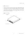
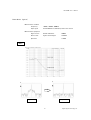
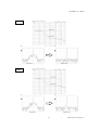
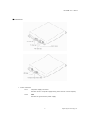
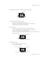
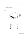
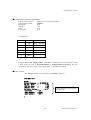
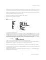
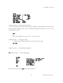
JITTER FILTER JFIL-200MF USER’S MANUAL Version 1.2 DIGITAL SIGNAL TECHNOLOGY, INC. 1-7-30, Higashi Benzai, Asaka, Saitama 351-0022, Japan TEL 81-48-468-6094 FAX 81-48-468-6210 http://www.dst.co.jp/en JFIL-200MF User’s Manual CONTENTS Function description ・・・・・・・・・・・・・ 3 Contents of package ・・・・・・・・・・・・・ 3 Electrical specification ・・・・・・・・・・・・・ 4 Connections ・・・・・・・・・・・・・ 7 Outline ・・・・・・・・・・・・・ 9 Communication requirements ・・・・・・・・・・・・・ 10 How to control ・・・・・・・・・・・・・ 10 Main mode ・・・・・・・・・・・・・ 11 Sub mode ・・・・・・・・・・・・・ 13 Option ・・・・・・・・・・・・・ 15 Handling Precautions ・・・・・・・・・・・・・ 15 2 Digital Signal Technology, Inc. JFIL-200MF User’s Manual ■Function description Using high purity VCXO and its narrow band pass characteristics of PLL and DDS, JFIL-200MF can be able to filter clock jitter and spurious within the range of 10MHz ~ 200MHz. JFIL-200MF has one TTL (CMOS) logic or LVDS level input and one TTL level output and two LVDS level outputs. The output signal phase can be controlled in the range of 0~360°. The settings can be controlled by serial data and all setting parameters can be memorized into EEPROM. As an option, LVC-232C is available in case of connecting to PC communication port for your convenience. ■Contents of the package ・JFIL-200M ×1 ・User’s manual ×1 3 Digital Signal Technology, Inc. JFIL-200MF User’s Manual ■Electric specification ・Power supply +5V~+7V 1A ・Frequency range 10MHz~200MHz ・Frequency lock range ±30ppm ・Frequency resolution 1Hz ・Phase offset range 0~360° ・Phase resolution 1° ・Phase stability 10ps/℃ (In case of 100MHz, it is equivalent to 9deg. from 25℃ to 50℃) ・Input level TTL (CMOS) (+5V、+3.3V、HiZ、50Ω selectable) or LVDS With input threshold setting possible ・Output level TTL (+5V、+3.3V selection possible 、50Ω drive possible) ×1 LVDS ×2 ・Spurious(except harmonics) less than -40dBc ・Phase Noise Refer to the graph on the next page ・PLL lock time less than 200ms ・Interface Asynchronous serial data 3V CMOS level An optional RS-232C level converter board is available. Connector: Pin Header (6pin) . ■Environmental condition ・operating temperature range 0℃ ~ +50℃ ■Dimension W135×H16.5×D100 (mm) 4 Digital Signal Technology, Inc. JFIL-200MF User’s Manual Phase Noise (typical ) Measurement condition Frequency 10MHz, 100MHz, 200MHz Input signal Phase Modulation (0.5rad) by white noise source Measurement equipment Signal source Rohde & Schwarz SME03 Phase noise Agilent Technologies E5052A Spectrum FSQ26 10MHz Input clock Output clock 5 Digital Signal Technology, Inc. JFIL-200MF User’s Manual 100MHz Input clock Output clock 200MHz Input clock Output clock 6 Digital Signal Technology, Inc. JFIL-200MF User’s Manual ■Connections 1. Power connector Pin1: +5V power supply connector Connect +4.75~+7V power supply having more than 1A current capacity Pin2: GND Connect the ground of the power supply 7 Digital Signal Technology, Inc. JFIL-200MF User’s Manual 2. LVDS clock input connector --- 2.54mm pitch 6 pin header terminal LVDS INJ4 1 GND GND LVDS IN LVDS IN+ 3. TTL(C-MOS) clock input connector – SMB +5V or +3.3V can be selected at the logic level. HiZ or 50Ω can be selected for the input impedance by serial command. Threshold level can be adjusted by serial command. 4. Serial comm. port This is a port for serial communication for setting frequency and so on. Interface is 3V CMOS level, but RS-232C level converter is available as an option in order to connect to PC communication port. The connector is a 2.54mm pitch with 6pin header terminal. 1 pin is TxD and 2 pin is RxD as shown below. TxD(Host RxD) J6 1 GND RS-232C RxD (Host TxD) 5. LVDS output connector This is a 2.54mm pitch 6 pin header terminal. There are two LVDS outputs. LVDS1 OUT- GND LVDS2 OUT+ J7 1 LVDS1 OUT+ LVDS OUT 8 LVDS2 OUT- Digital Signal Technology, Inc. JFIL-200MF User’s Manual 6. TTL output connector— SMB 7. TTL output level selection pin It can be selected the voltage of TTL output. Short +5V(JP1) or +3.3V(JP2) with a jumper plug. ■Outline A hole for installation 4 places 9 Digital Signal Technology, Inc. JFIL-200MF User’s Manual ■Communication interface requirements Type of Communication Communication speed Data length Stop bit Parity Flow control Asynchronous serial communication 9600BPS 8 bit 1 bit none none Pin assignment pin# signal signal direction 1 TxD JFIL→Terminal 2 RxD 3 GND 4 GND 5 GND 6 GND ← The signal level of JFIL-200MF is CMOS +3.3V. When a serial port of PC is used, interface it with a level convert IC such as MAX3232E(MAXIM) or ADM3202(ANALOG DEVICES). For your convenience, the level converter board “LVC-232C” is available as an option. ■How to control The following message is returned when JFIL-200MF is power on. JFIL-200M V1.0 STATUS Current Frequency TTL Out Phase LVDS1 Out Phase LVDS2 Out Phase VCO Control Voltage Input Signal Input Impedance Input Threshold = = = = = = = = 10 000 000 0 0 0 1.66 TTL 50ohm 0.8 V Hz Deg Deg Deg V This is just an example. The status depends on how the unit has been set. * 10 Digital Signal Technology, Inc. JFIL-200MF User’s Manual After the prompt “*” has been returned, the commands can be entered. There are two modes in command menu, main menu mode and sub menu mode. In main menu mode, the system control command such as frequency setting and phase setting can be done. In sub menu mode, input setting command such as a input signal, input impedance and input threshold can be set. Enter space code (20hex) after each command then enter argument. Then enter return key (0Dhex) as a delimiter. ■Main menu mode MAIN MENU F_xxx P1_xxx P2_xxx P3_xxx V STS SAVE SUB HELP = Frequency Set = TTL Out Phase Set = LVDS1 Out Phase Set = LVDS2 Out Phase Set = VCO Control Voltage Monitor = Status = SAVE = SUB Mode Entry = Command List *1 _ = Space *2 x = Parameters 1. F command – Frequency setting The output frequencies can be set in 1Hz step within the range of 10MHz~200MHz. First enter “F”, space code(20hex) and then frequency value. The frequency setting format is allowed in four different ways, MHz unit input, KHz unit input and Hz unit input. Add M or K after the setting value for distinguishing the unit. When the data has been set with MHz unit or KHz unit, each Hz part would be ignored. When JFIL-200MF received the data correctly, it returns VCO control voltage and “*”(2Ahex) as a prompt. For example *F 10M VCO Control Voltage = 1.65 V Make sure the VCO control voltage is within the specified range (0.5V-2.5V). When the data received incorrectly or some errors occurred during the transfer, “INVALID DATA” is returned. After the “*”(2Ahex) is returned, then you can enter the new command. Each time the frequency data is set continuously, be sure “*”(2A hex) is returned after each command. ** Please note that even if the frequency is set beyond 200MHz, it would be accepted but the quality of the signal would not be guaranteed. Here are some examples how to set frequencies. Please note hat under score “_” means SPACE (20hex) and (CR) means return code (0hex). 11 Digital Signal Technology, Inc. JFIL-200MF User’s Manual ・How to set on MHz unit F_100M (CR) →100MHz (100,000,000Hz) ・How to set on KHz unit F_20000K (CR) →20000KHz (20MHz = 20,000,000.000Hz) ・How to set on Hz unit F_123000000 (CR) →123MHz (123,000,000.000Hz) 2. P1, P2, P3 command – To set Phase Offset Phase offset can be set in 1°step within the range of 0°~ 360°. There are three phase commands P1, P2 and P3. “P1” is for TTL output, “P2” is for LVDS1 and “P3” is for LVDS2. Then, enter space code (20hex) and enter phase value. When JFIL-200MF received the data correctly, it returns “*”(2A hex) as a prompt. When the data received incorrectly or some errors occurred during the transfer, “INVALID DATA” is returned. A new command or a revised command is required. Each time the phase data is set continuously, be sure “*”(2A hex) is returned after each command. P1_90 (CR) →TTL(CMOS)output phase offset will be moved from 0 to 90° P2_180 (CR) →LVDS1 output phase offset will be moved from 0 to 180° 3. V command – VCO control voltage is displayed. Refer to “Caution of Page 17 for more details. 4. STS command – The current status such as frequency, phase offset, VCO control voltage, Input signal, Input impedance and Input threshold is displayed as below. 12 Digital Signal Technology, Inc. JFIL-200MF User’s Manual STATUS Current Frequency TTL Out Phase LVDS1 Out Phase LVDS2 Out Phase VCO Control Voltage Input Signal Input Impedance Input Threshold = = = = = = = = 10 000 000 0 0 0 1.66 TTL 50ohm 0.8 V Hz Deg Deg Deg V 5. SAVE command – To memorize the setting value The current frequency, phase offset, input signal, input impedance, input threshold can be memorized. If the command was completed, “Done” and “*” would be returned. When the power is on next time, the stored data can be output. Done * After these commands was returned, then, turn the power off. 6. SUB command ---- To change the mode To change the main mode to sub mode, or to put it back to main mode EXIT (CR) 7. HELP command ---- All commands are displayed. ■Sub menu mode ---- To set input signals SUB MENU SEL_x Z_x TH_xxx EXIT HELP = Input Level 1:TTL(CMOS) 0:LVDS = Input Impedance 1:HiZ 0:50ohm = Input Threshold 0.0 - 3.0 = Return to Main = Sub Command List *1 _ = Space *2 x = Parameters SUB* Note: In this sub menu mode, “SUB*” is returned instead of “*” 13 Digital Signal Technology, Inc. JFIL-200MF User’s Manual 1. SEL command ---- To select TTL or LVDS “SEL 1” --- TTL(CMOS) “SEL 0” --- LVDS 2. Z command ---- To select input impedance “Z 1” --- High impedance “Z 0” --- 50Ω 3. TH command ---- T set input signal threshold voltage It can be set in 0.1V step within the range of 0.0~3.0V. For example, TH_0.8(CR) 4. EXIT command ---- To end the sub mode To end the sub mode and return to the main mode, this command is used. 5. HELP command ---- all sub mode commands are displayed. ■Cautions on setting 1. Frequency settings As JFIL-200MF has quite narrow frequency lock range because of using TCXO, input correct frequency (within ±30ppm). Frequency value concludes from the VCO control voltage which is displayed with F command, V command and STS command. Set a correct frequency with VCO control voltage to be in the range of 0.50V~2.50V. Especially to make most of lock range, VCO control voltage can be set 1.65V (center value). 2. Phase offset settings Phase offset can be set per each output. Please note that even though the phase offset was set 0(Zero), the phase difference from input wouldn’t always be 0(Zero) because of JFIL-200M’s nature quality. The phasing between LVDS and LVDS2 output has been finished, but the phasing between TTL and LVDS has not. Again, set each output phase offset. 14 Digital Signal Technology, Inc. JFIL-200MF User’s Manual 3. Input threshold setting Input signal threshold is 0.8V as a standard. The setting voltage can be changed according to the drive capacity but about ±0.2V error range may be occurred. 4. PLL lock time After the signal was input, it would take maximum 200ms to reach lock status. ■Option RS-232C level converter LVC-232C ■ Handling Precautions (1) Use the low noise power supply. When the switching power supply is used, use a noise filter to reduce switching noise though the power supply. (2) The voltage will be dropped upon wiring from the power supply to JFIL-200MF as maximum 1A electrical current is running in JFIL-200MF. To apply more than 5V current is recommended . (3) Pay attention airflow and thermal resistance when embedded to prevent not to raise temperature of the unit. ・Descriptions of this manual are subject to change without notice. ・No portion of this manual can be reproduced without the permission of DS Technology, Inc. ・DS Technology Inc assumes no liability for damages that may occur as a result of handling by users. ・The contents of this manual do not apply to the warranty in executing an industrial property or other rights, nor permission for the right of execution. ・DS Technology Inc assumes no responsibility for the third party’s industrial property accrued from using the circuits described in this manual. DIGITAL SIGNAL TECHNOLOGY, INC. 15 Digital Signal Technology, Inc.