1
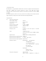
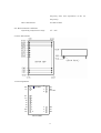
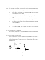
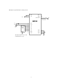
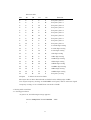
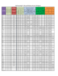
PCV-50F
FREQUENCY CONVERTER
USER’S MANUAL
History
rev1.0
2/1/2003
first edition issued
rev1.1
3/1/2003
consumption current revised
rev1.2
3/1/2004
10M→REF revised
DIGITAL SIGNAL TECHNOLOGY, INC.
1-7-30, Higashi Benzai, Asaka, Saitama, 351-0022, Japan
TEL 81-48-468-6094
Email : [email protected]
http://www.dst.co.jp/en
1
FAX 81-48-468-6210
1. Functional outline
The PCV-50F is a programmable oscillator that can take out signals of desired frequencies
from 1Hz to 50MHz with 0.001Hz resolution by using a 48-bit DDS (direct digital
synthesizer). The external reference frequency can be input as desired in a range of 7MHz
to 50MHz.
The output frequency can have an accuracy based on the stability of the external reference
signal. Frequency settings can be made with serial data and parallel data.
2. Specifications
2-1.
Electrical specifications
Power supply voltage
+5V±5%
Consumption current
500mA or less
Output level
CMOS
Output frequency range
0.001Hz - 50MHz
Frequency resolution
1mHz (0.001Hz)
Output waveform duty
50%±5%
Frequency error
0.46μHz or less with respect to external
reference
Jitter
±100pS rms or less
(cycle-to-cycle jitter value at 5MHz or higher
frequency)
Spurious level
40dBc or more (excluding harmonics)
External reference signal frequency 10MHz±5%
External reference signal level
2 - 5Vp-p
Duty 50±10%
External reference input impedance 470Ω or more
Frequency control
Parallel input
Six signal lines
4-bit BCD input
1-bit digit/data selection
1-bit
reference/output
frequency
data selection
1-bit strobe signal
Serial input
9600bps, 8 bits
No parity, 1 stop bit
Frequency setting time
Within 250mS
(Time between completion of setting of
2
frequency data and acquisition of the set
frequency)
Outer dimensions
61x46x13 (mm)
2-2. Environmental conditions
Operating temperature range
0℃ - 50℃
3. Outer dimensions
4. Pin assignments
GND
1
+5V
2
PIN1 MARK
16
REF
17
GND
18
FOUT/REF
GND
SET
3
A/D
4
D0
5
D1
6
D2
7
D3
8
13
RXD
9
12
OUT
TXD
10
11
GND
(TOP VIEW)
3
5. Pin names and descriptions
Pin No.
Name
Description
1
GND
Power supply/signal GND.
2
+5V
Power supply pin, to which +5V±5% should be supplied.
3
SET
Strobe signal for setting with parallel data.
As it is pulled up internally, data of A/D and D0 to D3 are read
internally by connecting it to GND.
Data is loaded on falling edge.
4
A/D
Select digit or numerical value for parallel data D0 to D3.
Set digit of 7-digit frequency data you want to change by H
(open).
Set the numerical value for selected digit by L (short-circuited
to GND)
It is pulled up internally.
5
D0
Input of frequency data digit or numerical data bit 0 (20).
6
D1
Input of frequency data digit or numerical data bit 1 (21).
7
D2
Input of frequency data digit or numerical data bit 2 (22).
8
D3
Input of frequency data digit or numerical data bit 3 (23).
9
RXD
Asynchronous serial data input pin.
Level is TTL-compatible CMOS.
When not in use, open it because the input is pulled up.
10
TXD
Asynchronous serial data output pin.
Level is TTL-compatible CMOS.
When not in use, open it.
11
GND
Power supply/signal GND.
12
OUT
Output terminal.
13
GND
Power supply/signal GND.
14
FOUT/REF
Input pin to select input of output frequency or reference signal
frequency data for frequency setting in parallel: H (open) and L
(short-circuited to GND) result in selection of output frequency
and reference signal frequency, respectively.
15
GND
Power supply/signal GND.
16
REF
Desired external clock input.
Remark: Pin No. 3, 4, 5, 6, 7, 8, 9, and 14 are pulled up by 10KΩ.
4
6. How to set frequencies with parallel data
Setting data includes reference frequency and output frequency, either of which is
determined by the FOUT/REF pin.
6-1. REF frequency setting
The reference signal frequency can be set in units of 1 mHz. Since the maximum frequency
of the reference signal is 50MHz, it is necessary to input frequency data at up to 11 digits
by the following procedures. In the reference signal setting mode, set FOUT/REF to LOW
level (short-circuited to GND). Next, select the digit to input, and then set the frequency
data for that digit. Select whether the BCD SW corresponds to digit or frequency data by
the A/D input. For example, how to set for inputting 16,000,000Hz is shown below.
(a)
Open S2, set the DIP SW to 0 (digit of 0.001Hz), and push S1 for
inputting (short-circuited to GND).
(b)
Close S2 (short-circuited to GND), set the BCD SW to 0 (frequency data
at the digit of 0.001Hz), and push S1. Now, frequency data is set at one
digit.
(c)
Also, set at the digit of 0.01Hz as in (a) and (b) by setting the BCD SW to
1 (digit of 0.01Hz) and pushing S1 for digit setting.
(d)
In a similar manner, set the frequency data from the digit of 0.1Hz to the
digit of 100KHz to 0.
(e)
At the digit of 1MHz, open S2, set the BCD SW to 9, push S1, and then
close S2, set the BCD SW to 6, and push S1.
(f)
At the digit of 10MHz, open S1, set the BCD SW to A, push S1, and then
close S2, set the BCD SW to 1, and push S1.
(Remark)
Since the input buffer of parallel data is initially set to “0” immediately
after power-on, “0” data can be omitted. In the above example, (a) to (d)
can be omitted.
(Caution)
Keep in mind that if the REF signal of a frequency higher than the set
reference frequency is input, the consumption current will increase, and
if this state is continued for a long time, the device may be damaged.
6-2. Output frequency setting
The output frequency can also be set in units of 1 mHz. Since the maximum frequency of
the output is 50MHz, it is necessary to input frequency data at up to 11 digits by the
5
following procedures. In the output frequency setting mode, set FOUT/REF to HIGH level
(open). Next, select the digit to input, and then set the frequency data for that digit. Select
whether the BCD SW corresponds to digit or frequency data by the A/D input. For example,
the method of setting for inputting 43,000,000Hz is shown below.
(a)
Open S2, set the DIP SW to 0 (digit of 0.001Hz), and push S1 for
inputting (short-circuit to GND).
(b)
Close S2 (short-circuited to GND), set the BCD SW to 0 (frequency data
at the digit of 0.001Hz), and push S1. Now, frequency data is set at one
digit.
(c)
Also, set at the digit of 0.01Hz as in (a) and (b) by setting the BCD SW to
1 (digit of 0.01Hz) and pushing S1 for digit setting.
(d)
In a similar manner, set the frequency data from the digit of 0.1Hz to the
digit of 100KHz to 0.
(e)
At the digit of 1MHz, open S2, set the BCD SW to 9, push S1, and then
close S2, set the BCD SW to 3, and push S1.
(f)
At the digit of 10MHz, open S1, set the BCD SW to A, push S1, and then
close S2, set the BCD SW to 4, and push S1.
6-3. How to save frequency by parallel data
For saving the set frequency in the built-in EEPROM semipermanently, open S2,
set the BCD SW to E (10), and push S1.
6-4. Caution for setting data consecutively
Since the PC performs frequency setting processing immediately after setting of
frequency data, if settings are made continuously, this processing will not be
performed in time. If you set one frequency, set a new frequency after a lapse of
200mS or more.
(See the timing chart shown below.)
>60ns
>100ns
A/D
D0-D3
FOUT/REF
>100ns
SET
>200ms
Parallel data timing chart
6
Example of parallel data setting circuit
+5V
1
GND
2
+5V
REF
16
GND
15
14
FOUT/REF
OPEN:FOUT
SHORT:REF
PCV-50
S1
3
SET
S2
4
A/D
5
D0
6
D1
7
D2
8
D3
GND
13
9
RXD
OUT
12
10
TXD
GND
11
1
BCD 2
SW
4
8
COM
BCD SWはコンプリメンタリー
The BCD
SW in use is the
タイプを使用します
complementary type.
7
S3
Function table
A/D
D3
D2
D1
L
L
L
L
L
Frequency data 0
L
L
L
L
H
Frequency data 1
L
L
L
H
L
Frequency data 2
L
L
L
H
H
Frequency data 3
L
L
H
L
L
Frequency data 4
L
L
H
L
H
Frequency data 5
L
L
H
H
L
Frequency data 6
L
L
H
H
H
Frequency data 7
L
H
L
L
L
Frequency data 8
L
H
L
L
H
Frequency data 9
H
L
L
L
L
0.001Hz digit setting
H
L
L
L
H
0.01Hz digit setting
H
L
L
H
L
0.1Hz digit setting
H
L
L
H
H
1Hz digit setting
H
L
H
L
L
10Hz digit setting
H
L
H
L
H
100Hz digit setting
H
L
H
H
L
1KHz digit setting
H
L
H
H
H
10KHz digit setting
H
H
L
L
L
100KHz digit setting
H
H
L
L
H
1MHz digit setting
H
H
L
H
L
10MHz digit setting
H
H
H
H
L
Frequency saving
H: Open
D0
Function
L: Short-circuited to GND
The input data of D0 to D3 and A/D are loaded on the falling edge of SET.
For output frequency setting, set FOUT/REF to H (open), and for reference signal
frequency setting, set it to LOW (short-circuited to GND).
7. Setting with serial data
7-1. Setting procedures
At power-on, the following message appears.
PCV50 FREQUENCY CONVERTER
*
8
VX.X
When the prompt “*” is returned from the PCV50F, frequency data can be input.
If data is input properly, the prompt “*” is returned, and the input frequency is
output.
If the input frequency is invalid, “INVALID DATA” is returned.
For setting the frequency consecutively, transmit frequency data, and confirm that
the prompt “*” is returned, and then input next frequency data.
The frequency can be input in MHz, KHz, Hz, or mHz (0.001Hz) together with a
decimal point.
For inputting the reference frequency, prepend the letter “R” to the frequency
data.
The following table shows an example of data for setting the reference frequency
to 10.25MHz.
R
1
0
・
2
5
52
31
30
2E
32
35
hex
hex
hex
hex
hex
hex
M
CR
4D
OD
hex
hex
The following table shows an example setting of the output frequency. The data for
setting an output frequency of 12.345678012MHz in MHz is shown below.
1
2
・
3
4
5
6
7
8
31
32
2E
33
34
35
36
37
hex
hex
hex
hex
hex
hex
hex
hex
9
38
hex
0
1
2
M
CR
39
30
31
32
4D
OD
hex
hex
hex
hex
hex
hex
The data for inputting the above frequency in mH is shown below.
1
2
3
4
5
6
7
8
31
32
33
34
35
36
37
38
hex
hex
hex
hex
hex
hex
hex
hex
9
39
hex
0
1
2
m
CR
30
31
32
6D
OD
hex
hex
hex
hex
hex
7-2. How to save frequency by serial data
For saving the set frequency in the built-in EEPROM, transmit the “SAVE”
command as shown below.
If it is written properly, the message “EEPROM SAVED!” is returned.
S
A
V
E
CR
53
hex
41
hex
56
hex
45
hex
0D
hex
7-3. Level converter with RS-232C
Since the level of PCV50F serial data is CMOS, such a level converter as shown below is
required for use in connection with a PC serial port.
9
Example of serial data setting circuit
7-4. Caution for setting reference frequency
In setting the reference frequency, if a frequency higher than the set reference
frequency is added as the REF signal, the consumption current will increase
significantly depending on the set value.
If this state is left for a long time, the device may be damaged.
Use the REF frequency and set value as properly adjusted.
8. Shipping inspection
8-1. Electrical inspection
100% inspection shall be performed for the electrical specifications in 2-1.
8-2. Appearance inspection
Inspection shall be performed for contamination and bends in pins.
10
9. Other
9-1. In the event of any doubt arising about these specifications, discussion and resolution
shall be made by arrangement.
9-2. This product, which employs a CMOS device, may be easily damaged by static
electricity.
9-3. Keep in mind that immersion cleaning is not allowed.
9-4. Special damp proof control is not necessary.
10. Warranty
If any defect is found due to the manufacturer’s improper production or design
within one year after delivery, repair or replacement shall be performed at the
manufacturer’s responsibility.
・ Descriptions in this manual are subject to change without notice.
・ No part of this manual may be reproduced without our permission.
・ We shall assume no liability for any user damage as a result of an
accident, etc.
・ Descriptions in this manual shall not guarantee the practice of
industrial property and other rights or grant a license for them.
・ We shall assume no liability for any third party’s industrial property
rights attributable to the use of circuits, etc., described in this manual.
Digital Signal Technology, Inc.
11