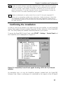
1
PowerDAQ AO Series User Manual
PD2/PDXI-AO High-Density Analog-Output Boards
PD2/PDXI-AO-HS High-Speed Analog-Output Boards
PD2-AO-HC High-Current Analog-Output Boards
August 2004 Edition
PN Man-AO-4-0804
© Copyright 1998-2004 United Electronic Industries, Inc. All rights reserved
No part of this publication may be reproduced, stored in a retrieval system, or
transmitted, in any form by any means, electronic, mechanical, by photocopying,
recording, or otherwise without prior written permission.
Fourth Edition
August 2004 Printing
Information furnished in this manual is believed to be accurate and reliable. However,
no responsibility is assumed for its use, or for any infringements of patents or other
rights of third parties that may result from its use.
All product names listed are trademarks or trade names of their respective companies.
See UEI’s website for complete Terms and Conditions of sale:
http://www.ueidaq.com/company/terms.asp
Contacting United Electronic Industries
Mailing Address:
611 Neponset St
Canton, MA 02021
U.S.A.
Support:
Telephone:
(781) 821-2890
Fax:
(781) 821-2891
Also see the FAQs and online “Live Help” feature on our web site.
Internet Access:
Support
[email protected]
Web site
www.ueidaq.com
FTP site
ftp://ftp.ueidaq.com
Table of Contents
1. Introduction ................................................................................................. 1
Who should read this manual? .................................................................................... 1
Conventions.................................................................................................................2
Organization of this manual....................................................................................... 3
2. AO Series Features ....................................................................................5
Overview .................................................................................................................... 5
Features...................................................................................................................... 5
Analog-output applications ........................................................................................ 6
AO Series models.........................................................................................................7
3. Installation and Configuration................................................................9
Before you begin........................................................................................................ 9
System requirements .................................................................................................. 9
Packing list ................................................................................................................. 9
Software installation.................................................................................................. 10
Installing the SDK and Windows driver ...................................................................... 10
Linux driver.................................................................................................................11
Realtime Linux kernel patches.....................................................................................11
Compiling and installing Linux kernels ....................................................................... 12
Loading and testing the Linux driver.......................................................................... 12
QNX driver ................................................................................................................ 13
Compiling and Installing the QNX driver.................................................................... 13
Loading and testing the QNX driver .......................................................................... 13
Using the QNX library from C/C++ .......................................................................... 14
Hardware installation................................................................................................. 15
Base address, DMA and interrupt settings................................................................. 16
Confirming the installation ........................................................................................ 17
Synchronizing multiple boards ................................................................................... 18
Remote sensing ......................................................................................................... 19
Connectors and pinouts............................................................................................ 20
PD2-AO-8/16, -16/16 and -32/16............................................................................ 20
PD2-AO-32/16HC......................................................................................................25
PD2-AO-96/16 ..........................................................................................................26
PD2-AO-96/16 ..........................................................................................................27
Panel connection, PD2 ...............................................................................................29
PDXI-AO-8/16, -16/16, -32/16 ................................................................................ 30
Panel connection, PDXI..............................................................................................35
4. Architecture ..............................................................................................37
Functional Overview...................................................................................................37
The Analog Output subsystem.................................................................................. 39
i
Table of Contents
The Digital I/O subsystem.........................................................................................40
Counter/timer subsystem..........................................................................................40
Interrupt lines.............................................................................................................41
Programming Model ..................................................................................................41
Modes and performance........................................................................................... 42
Programming Techniques ..........................................................................................44
General procedures ...................................................................................................44
Opening a subsystem................................................................................................45
API calls for opening/closing a subsystem ................................................................45
Driver structure .........................................................................................................46
Data format.............................................................................................................. 47
Output datapath .......................................................................................................48
Buffer structure ........................................................................................................49
Frame........................................................................................................................49
Scan ..........................................................................................................................49
Channel string...........................................................................................................49
5. Analog-Output Subsystem.................................................................... 51
Data/control flow......................................................................................................51
Operating modes and parameters ..............................................................................51
Output modes............................................................................................................51
Transfer modes ......................................................................................................... 52
Update methods ....................................................................................................... 52
Update rates (speeds)............................................................................................... 53
Output ranges........................................................................................................... 53
Calibration subsystem ...............................................................................................54
Resets .......................................................................................................................54
Clocking and triggering............................................................................................. 55
Simultaneous updates ............................................................................................... 57
Programming onboard logic......................................................................................58
Single-Point Update mode ........................................................................................58
Calling sequence .......................................................................................................58
Buffered updates ...................................................................................................... 59
Event-Based Waveform mode................................................................................... 59
Waveform Regenerate mode ....................................................................................60
Direct DSP Buffer Access mode ................................................................................60
Buffered update settings .......................................................................................... 62
Buffered update examples ........................................................................................ 63
Buffered update configuration parameters ...............................................................64
Buffer data format ................................................................................................... 65
AO subsystem configuration .....................................................................................66
Hardware-update channel setup ............................................................................... 67
Channel-list configuration......................................................................................... 67
Programming model for buffered modes................................................................... 71
6. Digital I/O Subsystem ............................................................................ 81
Architecture .............................................................................................................. 81
ii
Table of Contents
Programming Techniques........................................................................................... 81
Polled I/O.................................................................................................................. 81
Change-of-state interrupts on digital input.............................................................. 82
7. Counter/Timer Subsystem.....................................................................85
Architecture.............................................................................................................. 85
Programming the counter/timers ............................................................................. 86
8. Software Support ....................................................................................89
PowerDAQ SDK Structure ......................................................................................... 89
Windows device drivers ............................................................................................ 90
Windows DLLs .......................................................................................................... 90
Language libraries...................................................................................................... 91
Include files ............................................................................................................... 91
Linux support.............................................................................................................92
QNX support ............................................................................................................ 93
Example programs .................................................................................................... 93
Third-party software support ................................................................................... 94
LabVIEW VIs for analog output ................................................................................ 95
Appendix A: Specifications.........................................................................99
PDx-AO specifications .............................................................................................. 99
Analog-output subsystem......................................................................................... 99
Digital Input/Output subsystem............................................................................... 100
DSP-based subsystems .............................................................................................101
DC electrical characteristics for DSP-based subsystems ............................................101
Appendix B: Accessories ...........................................................................103
Screw-Terminal Panels (PD2/PDXI) ......................................................................... 103
BNC Panels (PD2/PDXI)........................................................................................... 103
Cables (PD2/PDXI) .................................................................................................. 104
Other Accessories (PD2/PDXI)................................................................................. 104
OEM Header Distribution Connector........................................................................ 105
Appendix C: Board-level AO Command Format................................. 107
Single-Point Update commands............................................................................... 109
Address space/commands ....................................................................................... 109
Non-buffered mode control bits ..............................................................................110
Write commands ......................................................................................................110
Read commands ........................................................................................................111
Call-sequence example ............................................................................................. 112
Using AO functions of the SDK................................................................................ 112
Using _PdDIO256RegXX functions........................................................................... 112
Appendix D: Calibration.............................................................................113
Calibration IC and DAC assignments.........................................................................114
Appendix E: Advanced Circular Buffer ...................................................119
iii
Table of Contents
Glossary ........................................................................................................ 123
Index...............................................................................................................141
Reader Feedback ........................................................................................145
iv
1. Introduction
This manual describes the features and functions of the PowerDAQ AO Series of
analog-output boards. These high-performance systems support high-density 16-bit
analog output, digital I/O, and user counter/timers for either the PCI bus (PD2 family)
or PXI/CompactPCI-bus (PDXI family). The cards covered in this manual are the
following:
•
•
•
•
•
•
•
PD2-AO-8/16
PD2-AO-16/16
PD2-AO-32/16
PD2-AO-32/16HC
PD2-AO-32/16HS
PD2-AO-96/16
PD2-AO-96/16HS
•
•
•
•
•
•
PDXI-AO-8/16
PDXI-AO-8/16HS
PDXI-AO-16/16
PDXI-AO-16/16HS
PDXI-AO-32/16
PDXI-AO-32/16HS
Who should read this manual?
This manual has been designed to make the installation, configuration and operation of
our PowerDAQ analog-output boards as straightforward as possible. However, it
assumes that the user has basic PC skills and is familiar with Microsoft Windows
2000/NT/XP, QNX or Linux (Red Hat or Suse distributions) as well as leading realtime
patches (FSMLabs’ RTLinux and RTAI).
1
Chapter 1: Introduction
Conventions
To help you get the most out of this manual and our products, please note that we use
the following conventions:
TIP
Note
Tips are designed to highlight quick ways to get the job done, or reveal good
ideas you might not discover on your own.
Notes alert you to important information.
CAUTION! Caution advises you of precautions to take to avoid injury,
data loss, and damage to your boards or a system crash.
Text formatted in bold typeface generally represents text that should be entered
verbatim. For instance, it can represent a command, as in the following example: “You
can instruct users how to run setup using a command such as setup.exe.”
2
Chapter 1: Introduction
Organization of this manual
This PowerDAQ PDx-AO User Manual is organized as follows:
Chapter 1—Introduction
This chapter gives you an overview of PowerDAQ Analog Output Series board features,
the various models available and what you need to get started.
Chapter 2—AO Series Features Overview
This chapter provides an overview of the key features of the PowerDAQ AO Series and
detailed information on the various models currently available.
Chapter 3—Installation and Configuration
This chapter explains how to install and configure your PowerDAQ AO Series board.
Among other things, it shows where various I/O connectors are located on the boards,
how to connect them (even when using remote sensing), and also shows their pinout
definitions.
Chapter 4—Architecture
This chapter discusses the functionality of the subsystems of your PowerDAQ AO Series
board, and it gives an overview of the programming model, showing how various cards
and software modules intercommunicate. It further reviews the key operating modes of
the AO subsystem, and then it introduces you to the buffer structure including the
concept of scans and frames.
Chapter 5—Analog-Output Subsystem
This chapter gives extensive details about this subsystem including the various operating
modes, performance parameters, clocking and triggering as well as details on how to
configure and program all these features. .
Chapter 6—Digital I/O Subsystem
This chapter reviews the architecture and key operating/programming principles you
need to take advantage of the digital I/O resources on an AO Series board.
Chapter 7—Counter/Timer Subsystem
This chapter gives the information you need to use the three onboard counter/timers
that are a feature of all AO Series boards.
Chapter 8—Support Software
This chapter provides an overview of the resources on the PowerDAQ SDK including a
discussion of the SDK structure, a review of key drivers, DLLs, libraries and include files,
details about programming under LabVIEW, and how to work with an OS other than
Windows. It wraps up with a review of key example programs.
3
Chapter 1: Introduction
Appendix A - Specifications
This chapter lists the PowerDAQ AO Series hardware specifications.
Appendix B - Accessories
This appendix provides a list of PowerDAQ accessories available for use with AO Series
boards.
Appendix C – Board-level AO Command Format
This section describes commands on the PowerDAQ AO boards that can be used for
low-level firmware or software programming. They also serve to help you better
understand AO board functionality.
Appendix D: Calibration
This section gives details on the structure that holds calibration values along with other
nonvolatile information
Appendix E: Advanced Circular Buffer
This application note describes the operation of the ACB, a section of host memory a
PowerDAQ board uses to alleviate many of the latency problems that arise with
Windows.
Glossary
This is an alphabetical listing of key terms you will encounter in working with
PowerDAQ cards and test systems in general.
Index
This is an alphabetical listing of the topics covered in this manual.
Feedback
We are interested in any feedback you might have concerning our products and
manuals. A Reader Evaluation form is available on the last page of the manual.
4
2. AO Series Features
This chapter provides an overview of the key features of PowerDAQ AO Series analogoutput cards and detailed information on the various models currently available. It also
lists what you need to get started.
Overview
Thank you for purchasing a PowerDAQ AO Series board. These advanced boards
feature an onboard DSP that allows simultaneous operation of all I/O subsystems
without host intervention. In addition, the DSP runs a firmware-based command
interpreter that makes it easy and convenient to program these cards from virtually any
programming language using the same API.
PowerDAQ AO Series boards are configured with either 8, 16, 32 or 96 independent
analog-output channels (PDXI versions are available with 32 channels max). They
feature 16-bit D/A converters and allow you to configure the startup states for each
channel (200 msec maximum delay between system reset and power-on value loading).
The on-board DSP and PCI interface allow you to use any or all of the three 24-bit
counter timers, high-speed IRQ/external clock lines, eight digital inputs and eight highdrive TTL digital outputs (that source 32 mA or sink 64 mA).
Features
The major features of PowerDAQ AO boards are:
• 24-bit Motorola 56301 digital signal processor running at 66 MHz (100 MHz on –HS
models)
• PCI host interface (PCI 2.1 compliant)
• 8, 16, 32 or 96 D/A converters, 16 bits, ±10V
Note
•
•
•
•
•
•
Custom output voltage ranges are available; contact UEI sales department for availability.
At this time, we offer ±2.5V, ±5V –10-0V and 0-10V configurations on special order.
DC to 100 kHz throughput per D/A
1.5 MHz per-board maximum aggregate update rate (3.2 MHz on
Fixed-length or unlimited-size channel lists
Asynchronous or simultaneous update modes for all D/As
Per-channel calibration
Single-ended outputs (AGND used as return)
-HS models)
5
Chapter 2: AO Series Features
•
•
•
•
•
•
•
•
•
•
Sense lines for each D/A—standard on PD2-AO-32/16HC; available upon request at
time of order for PD2-AO-8/16, -16/16 and -32/16; jumper-selectable on PDXI
models (only for output channels 0-15). Sense lines not available on high-density
96-channel PD2-AO-96/16 board.
User-defined power-up states for each D/A
Direct access to the output FIFO for advanced applications
Eight digital inputs
Eight digital outputs
Three 24-bit counter/timers
Counters, interrupt and synchronization inputs
On-board 2k-sample FIFO (located in DSP memory)
64k-sample FIFO upgrade option (comes standard on –HS models)
Drivers in PowerDAQ Software Suite for all popular operating systems, programming
languages and test applications.
Note For a full list of specifications, see Appendix A: Specifications.
Analog-output applications
PowerDAQ AO Series boards provide many powerful features that allow these boards
to cover a wide range of applications. The most common of these are:
• Process control
• ATE (automatic test equipment)
• Closed-loop servo control
• Motor control
• Complex continuous multichannel waveform generation
• Telecommunications equipment control.
The digital I/O subsystem finds use in these applications:
• Electromechanical relay control
• Solid-state relay interfacing
• Alarm-system sensors
• Digital motion control
The counter/timer subsystem finds use in these applications:
• Pulse-width modulation
• Frequency counting
• Pulse generation
Note The easiest way to expand the possibilities of an AO Series board is to use it in a system
along with a PD2/PDXI-MF(S) multifunction board.
6
Chapter 2: AO Series Features
AO Series models
PowerDAQ PDx-AO model numbers are derived as follows:
[Bus] – AO – [Channels] / [Resolution] [Options]
where for bus you can choose
• PD2
PCI bus
• PDXI
CompactPCI / PXI bus
and for options you can choose
• HC
high current
• HS
high speed (with 100-MHz DSP)
Models
AO Features
PD2-AO-8/16
PCI bus, 8 16-bit D/A channels
PD2-AO-16/16
PCI bus, 16 16-bit D/A channels
PD2-AO-32/16
PCI bus, 32 16-bit D/A channels
PD2-AO-32/16HC
PCI bus, 32 16-bit D/A channels, high current
PD2-AO-32/16HS
PCI bus, 32 16-bit D/A channels, high speed
PD2-AO-96/16
PCI bus, 96 16-bit D/A channels
PD2-AO-96/16HS
PCI bus, 96 16-bit D/A channels, high speed
PDXI-AO-8/16
PXI/CPCI bus, 8 16-bit D/A channels
PDXI-AO-8/16HS
PXI/CPCI bus, 8 16-bit D/A channels, high speed
PDXI-AO-16/16
PXI/CPCI bus, 16 16-bit D/A channels
PDXI-AO-16/16HS
PXI/CPCI bus, 16 16-bit D/A channels, high speed
PDXI-AO-32/16
PXI/CPCI bus, 32 16-bit D/A channels
PDXI-AO-32/16HS
PXI/CPCI bus, 32 16-bit D/A channels, high speed
Table 2.1—PowerDAQ AO Series models
All
•
•
•
•
PowerDAQ AO boards have the following additional features:
Digital inputs: Eight static lines
Digital outputs: Eight static lines
Clock/trigger/update lines
Counter/timers: Three 24-bits units (33 MHz clocked internally, 16.5 MHz clocked
externally)
7
3. Installation and
Configuration
This chapter describes the installation and configuration of the hardware and software
for a PowerDAQ AO Series board.
Before you begin
Before installing your PowerDAQ AO board, be sure to read and understand the
following information.
System requirements
To install and run a PowerDAQ AO board you need the following:
• A PCI-bus system, a PXI-bus system or a CompactPCI-bus system with a free slot, a
Pentium-class processor, and a BIOS compatible with the PCI Specifications 2.1 or
greater.
• Windows NT 4.0 / 2000 / XP, Linux, Realtime Linux or QNX operating system
Note PowerDAQ drivers starting with v3.0 do not support Windows 95/98/Me. Previous
versions of our drivers that do function with these earlier releases of Windows are
available from our Customer Support department.
•
•
At least 32M bytes of RAM for Windows NT, and 64M bytes for Windows
2000/XP. (Generally 64M bytes of RAM are required for the latest version of Linux,
and 16M bytes are needed for QNX. (With any OS, we recommend at least 128M of
RAM for best performance)
The PowerDAQ Software Suite CD, which ships with your AO Series board. You can
always download the latest version of this support software at no charge from
www.ueidaq.com/download
Packing list
In
•
•
•
your PowerDAQ package you should have received the following:
a PowerDAQ AO Series board
a calibration certificate
this User Manual
9
Chapter 3: Installation and Configuration
•
a CD containing the PowerDAQ Software Suite, including the full Software
Development Kit (SDK) and documentation.
CAUTION! PowerDAQ boards contain sensitive electronic components.
They are shipped in an anti-static bag to protect against electrostatic
charges that might damage the board. To avoid damage, you should:
• Ensure you are properly grounded with a wrist strap or some other
means.
• Discharge any static electricity by touching the metal part of your PC
while holding the board in its antistatic bag.
• When you remove the board from the antistatic bag, save the bag for
later possible use such as to store the board.
• Inspect the board for any damage. If you find any problems, notify
the UEI sales team or your distributor for instructions on how to
return the board.
Software installation
Note The PowerDAQ SDK must be installed before you plug in a PowerDAQ board to ensure
that the driver properly detects the board.
Note All third-party software must be installed prior to installing the PowerDAQ SDK. If you
added/installed any third-party software after you installed the PowerDAQ SDK, the best
way to ensure proper support for that package within the PowerDAQ environment is to
uninstall and reinstall it.
Installing the SDK and Windows driver
To install the PowerDAQ SDK:
1.
Start your PC and, if running Windows NT, 2000 or XP, log in as an
administrator.
2. Insert the PowerDAQ Software Suite CD into your CD-ROM drive. Windows
should automatically start the PowerDAQ Setup program. If you see the UEI
logo and then the PowerDAQ welcome screen, go to Step 6.
3. If the Setup program does not start automatically, select Run from the
Start menu.
4. Enter d:/setup.exe in the Open: textbox (substitute the correct drive letter
if D is not the one for your CD-ROM drive)
10
Chapter 3: Installation and Configuration
5. Click OK.
6. As the Setup program runs, it will ask you to enter information about your
PowerDAQ configuration. Unless you are an expert user and have specific
requirements, you should select a typical installation and accept the default
configuration.
7. If the Setup program asks for information about third-party software
packages that you do not have installed on your PC, leave the text box
blank and click the Next button.
8. When the installation is complete, restart your PC when prompted.
Note Never delete the PowerDAQ software from your PC’s hard disk directly. Because the
installation process modifies the Windows Registry, you must install or uninstall this
software only using appropriate programs such as the Uninstall utility in the PowerDAQ
folder or the Control Panel/Add-Remove Programs applet.
Linux driver
In order to compile the PowerDAQ kernel module and shared library, you must have a
correctly configured Linux kernel source tree. The best way to get one is to download a
tarball from kernel.org and compile your own kernel. PowerDAQ works with the 2.2,
2.4 and 2.6 Linux kernels.
At any time you can download the latest Linux driver from our web site
www.ueidaq.com. PowerDAQ boards always support the latest Linux driver.
Realtime Linux kernel patches
The PowerDAQ for Linux driver supports hard realtime operation when you augment
the base kernel with realtime patches. We have tested our products for operation with
the following two patches:
RTAI
If you want to use the realtime capabilities of a PowerDAQ card possible with the RTAI
kernel patch, you must first compile and install the RTAI software. Known working
versions are RTAI-24.1.4, RTAI-24.1.10, RTAI-24.1.12 and RTAI CVS. Edit the Makefile
and set the variable RTAI_DIR to the location of your RTAI installation. Compile the
driver with the option RTAI=1.
RTLinux (FSM Labs)
If you want to use the realtime capabilities of a PowerDAQ card possible with the
RTLinux kernel patch, you must first compile the RTLinux software (both the kernel and
the modules). Known working versions are 2.x and 3.x. Edit the Makefile and set the
variable RTLINUX_DIR to the location of your RTLinux installation. Compile the driver
with the option RTL=1 if you use the free version of RTLinux or RTLPRO=1 if you use
the Professional version.
11
Chapter 3: Installation and Configuration
Compiling and installing Linux kernels
Compile using 'make'. Doing so compiles the kernel module, the shared
library and the examples.
• To compile the driver for RTLinux, use 'make RTL=1' or 'make RTLPRO=1'
• To compile the driver for RTAI, use 'make RTAI=1'
• To compile the driver for Linux kernel 2.4.x or 2.6.x, use 'make'
Install the resulting driver using 'make install' as root. This installs the files:
/lib/modules/<<kernel version>>/misc/pwrdaq.o (for kernels 2.4.x)
/lib/modules/<<kernel version>>/misc/pwrdaq.ko (for kernels 2.6.x)
/usr/local/lib/libpowerdaq32.so.1.0.
Next run the depmode and ldconfig utilities to register those component with your
system.
The install script asks if you want to install the library. If you answer Y it then prompts
you for the location of LabVIEW on your file system and starts copying the VIs.
Loading and testing the Linux driver
Load the driver using 'modprobe pwrdaq' and test that it detects your boards by issuing
the command 'cat /proc/pwrdaq'. That command should list all the PowerDAQ boards
it finds on your system.
Note that if you want to install your own IRQ handler under RTLinux or RTAI you must
load the driver with the option "rqstirq=0" so that it doesn’t install any IRQ handler.
When you add this option, the buffered AI/AO/DI/DO functionality is no longer
available.
You can now run some examples to test your board:
• SingleAO tests the analog-output subsystem
• SingleDI tests the digital-input subsystem
• SingleDO tests the digital-output subsystem
• SingleUCT tests the counter/timer subsystem
You can set up your system to automatically load the PowerDAQ driver the first time it
is needed by adding the following line to the file
/etc/modules.conf:
alias char-major-61 pwrdaq
Using the PowerDAQ library from C/C++
The best way to start is to take one of the examples Makefile as a template. You must
include the following header files in your source code:
12
Chapter 3: Installation and Configuration
#include
#include
#include
#include
#include
#include
#include
<stdlib.h>
<stdint.h>
<sys/types.h>
<unistd.h>
"win_sdk_types.h"
"powerdaq.h"
"powerdaq32.h"
You must also link your application with the PowerDAQ shared library by adding "lpowerdaq32" to your linker options.
QNX driver
The PowerDAQ QNX driver is compatible with QNX ver 4.x and (6.x up to 6.3).
Compiling and Installing the QNX driver
Compile the driver using 'make'. Doing so compiles the resource manager, the shared
library and the examples. To compile the driver with debug output turned on use 'make
DEBUG=1'.
Install the QNX driver using 'make install' as root. This installs the files:
/usr/lib/libpwrdaq.so.1.0 (the low-level library)
/usr/lib/libpowerdaq32.so.1.0 (the library that interfaces with the resource manager)
/usr/bin/dev-pwrdaq (the resource manager)
Loading and testing the QNX driver
Run the resource manager in the background with the command "dev-pwrdaq&".
The resource manager can be started with the following options:
• -h
display help
• -i n
install interrupt handler if n=1 (default)
• -x n
set the transfer mode: 0 = normal, 1 = fast, 2 = DMA (default is 1)
• -p n
start the resource manager with priority set to n (0 < n < 40), the
default is 20
You can then run some of the examples to test your board:
• SingleAO tests the analog-output subsystem
• SingleDI tests the digital-input subsystem
• SingleDO tests the digital-output subsystem
• SingleUCT tests the counter/timer subsystem
You can set up your system to automatically start the PowerDAQ resource manager.
Create or edit the file /etc/rc.d/rc.local.
Add the following line at the end of rc.local: dev-pwrdaq&
13
Chapter 3: Installation and Configuration
Make it executable: "chmod +x /etc/rc/d/rc.local"
Using the QNX library from C/C++
The best way to start working with the QNX driver is to take one of the examples
Makefile as a template. You must include the following header files in your source
code:
#include
#include
#include
#include
#include
<stdio.h>
<stdint.h>
<stdlib.h>
<unistd.h>
<string.h>
#include
#include
#include
#include
"win2qnx.h"
"pd_hcaps.h"
"powerdaq.h"
"lib/powerdaq32.h"
You must also link your application with the PowerDAQ shared library by adding "lpowerdaq32" to your linker options.
14
Chapter 3: Installation and Configuration
Hardware installation
You can install a PD2-AO Series board in any PCI slot and a PDXI-AO Series board in
any I/O slot in a Compact PCI / PXI chassis. To install your PowerDAQ board:
1. Turn off your PC.
2. Remove the cover (as appropriate) and make sure you have clear access to
the slots.
3. Connect all desired cables that mount directly on the AO Series board (see
the section later in this chapter, “Connectors and pinouts” on page 20).
4. Find a free slot and remove any blank brackets that might be there.
TIP
To limit noise interference, install the board as far as possible from other
devices and hardware.
5. Insert the PDx-AO Series board into a free slot.
Note If a slot has not been used in a long time, clean the connector: Insert the PowerDAQ
board, immediately remove it and clean its edge connector with alcohol. Then put the
board back into the slot.
6. Insert the board and ensure that you have mounted it properly into the
slot.
7. Fasten the board’s mounting bracket to the PC with the screws that held
the blank bracket as appropriate.
8. If necessary, attach a cable to the card’s edge connector and also attach it
to a termination panel.
CAUTION! When working with a PDXI family card that requires the
PDXI-AO-CBL-96, please pay particular attention to the orientation of
the cable as shown in Figure 3.1; attaching the cable in the wrong
manner can result in damage to the card.
15
Chapter 3: Installation and Configuration
Figure 3.1—Cable layout for PDXI AO boards; J1 connects to the board, whereas
the two other ends connect to a screw-terminal panel.
9. Replace the PC’s cover if needed
10. Reapply power to the PC.
Base address, DMA and interrupt settings
When you power up your PC, the PCI bus automatically configures any PowerDAQ
boards that are installed. You need not set any base address, DMA channels or
interrupt levels.
Be aware, though, that performance problems can arise when the system has
insufficient interrupts, can’t assign a unique one to each peripheral, so a PowerDAQ
board must share an interrupt with another device. PowerDAQ boards are designed to
share interrupts, but we do not recommend that they do so with devices such as video
drivers, network cards, hard disks and especially USB ports. These devices tie up
interrupt lines extensively and can significantly delay response to an interrupt from a
data-acquisition subsystem. Although Windows NT/2000/XP are not realtime operating
systems, your PowerDAQ board is a real-time system within the PC thanks to its own
DSP and realtime firmware kernel.
Many motherboard manufacturers allow you to set an IRQ level to a particular PCI slot.
If you do not use your PC’s serial or parallel ports, you can disable them and use IRQ 3,
4, 5 or 7 for your data-acquisition boards.
16
Chapter 3: Installation and Configuration
Note
A data-acq card’s interrupt is generally assigned by the PC BIOS, and some PC systems
even let you reassign it during the boot process. If your motherboard has an Advanced
Interrupt Controller, simply enable it in the BIOS. This allows you to use more than 16
generic interrupt lines. If you don’t have this facility, use manual settings to assign the
interrupt to the PCI slot where PowerDAQ board is installed
Note
Modern motherboards can easily contain five or more PCI slots plus integrated PCI
devices such as networking modules and a video driver. Usually only three of these slots
are independent and don’t share interrupts with these host peripherals. Please refer to
your motherboard manual to find out which slots share interrupts and cannot be used for
fast data acquisition.
Confirming the installation
In order to confirm the operation of a board you have just installed, run the PowerDAQ
Control Panel applet that gets installed along with all other elements of the PowerDAQ
SDK. This utility displays all available PowerDAQ boards in your system.
To access the PowerDAQ Control Panel, select START > Settings > Control Panel and
the PowerDAQ icon is displayed as in Figure 3.2.
Figure 3.2—PowerDAQ Control Panel applet showing a PD2-AO-32/16 board
installed
An alternative test is to use the SimpleTest program installed with the PowerDAQ
Software Suite. Attach a oscilloscope or a multimeter to the outputs of the AO board.
17
Chapter 3: Installation and Configuration
Run the SimpleTest.exe program by selecting START > Programs > PowerDAQ >
Utilities > SimpleTest. This program shows all available information about the installed
board(s) and allows you to test all subsystems on the selected board. Set the analog
outputs to generate signals and verify that the desired signals appear on the DMM or
scope display.
Synchronizing multiple boards
In some cases you might wish to synchronize the operation of multiple AO Series cards.
For the PCI-bus PD2 versions, you can make synchronization connections either inside
or outside the PC chassis.
For internal connections, note that the J2 connector (described in detail in the section
“Connectors and pinouts” on page 20) includes a TMR2 Clock I/O pin. You connect this
pin to the TMR2 pin of another board with which you wish to synchronize operation.
We recommend you use a 100-200Ω series resistor for the clock connection between
the two cards. If you would like a preconfigured synchronization cable, contact the
factory.
For external synchronization, simply make all necessary connections for each card. A
common method is to use a PD-CBL-37 cable and a screw-terminal panel for each
card. Then simply wire the TMR2 Clock pins of the desired cards together (we still
recommend the use of 100-200Ω series resistors).
Note When synchronizing boards, first ensure that the software driver recognizes them all by
examining their status in the PowerDAQ AO Control Panel applet.
For PDXI boards, you can make all synchronization settings over the PXI backplane with
the PDXI Configurator software. Alternatively you can use the TMR2 pin on a screwterminal panel.
18
Chapter 3: Installation and Configuration
Remote sensing
Remote sensing eliminates errors that arise due to voltage drops in the leads connecting
the D/A output on the board to the load. When using the sense line the card can
achieve 16-bit accuracy at the rated output current. You connect the remote sense line
to the load as shown in Figure 3.3.
Figure 3.3—Connection of sense lines to a load
An AO Series board reads the feedback voltage on a given channel’s sense line and
adjusts the output correspondingly to compensate for losses in the leads going to the
load. The sense line carries very little current so you needn’t be concerned with
significant losses in that line.
The various families and products differ in how they implement sensing:
• PD2-AO-8/16, -16/16, -32/16: By default the factory installs sensing resistors (Rs).
If the user application requires sense lines, you should be sure to specify that fact
when placing your order. With sense resistors populated, you simplify wiring and
usually also get lower noise levels on the output. If sense lines are available on the
selected board, you should connect them with the corresponding output lines on the
PD-AO-STP terminal or at the destination of the output signal
• PD2-AO-32/16HC: Sense lines are standard. If you choose not to take advantage of
remote sensing, you should connect the sense lines to the corresponding output lines
on the terminal panel or directly on the board using the configuration jumpers that
are available for this purpose (a 2-mm jumper per channel, labeled by the channel
number on the silkscreen).
• PD2-AO-96/16: This board does not provide sense lines because of the large number
of D/As on this high-density board.
• PDXI-AO-8/16, -16/16, -32/16: These cards allows the use of sense lines on at most
16 channels by installing on-board jumpers.
19
Chapter 3: Installation and Configuration
Note The default sense line carries the same signal as the corresponding output on PD2-AO8/16, -16/16 and -32/16 boards because of noise considerations; large currents going
through the cable may force outputs to oscillate because the sense line picks up noise
from the surrounding lines.
Connectors and pinouts
PD2-AO-8/16, -16/16 and -32/16
The PCI-bus PD2-AO-8/16, -16/16 and -32/16 boards have two I/O connectors:
• J1: a 96-contact header for analog-output signals
• J2: a 36-way boxed IDC header for digital I/O, counter/timer and interrupt lines
UEI selected a pinout scheme for J1 that allows the PD2-AO-8/16, -16/16 and –32/16
as well as the PD2-MF(S) Series to share common accessories. Note that on PD2-AO8/16 and –16/16 that the AOut16-AOut31 lines and also the AOut16-AOut31 Sense lines
are connected to ground.
Figure 3.4—Connector layout for the PD2-AO-8/16, -16/16 and -32/16. J1
handles the analog outputs, while J2 carries digital I/O and interrupt signals.
20
Chapter 3: Installation and Configuration
Figure 3.5—Physical layout of J1 on PD2-AO-8/16, -16/16 and -32/16 boards
(view looking into the connector as mounted on the board).
Figure 3.6—Pin assignments for J1 on the PD2-AO-8/16. This connector handles
analog-output signals.
21
Chapter 3: Installation and Configuration
Figure 3.7— Pin assignments for J1 on the PD2-AO-16/16. This connector handles
analog output signals.
22
Chapter 3: Installation and Configuration
Figure 3.8— Pin assignments for J1 on the PD2-AO-32/16. This connector handles
analog output signals.
23
Chapter 3: Installation and Configuration
Figure 3.9—Physical layout of J2 on PD2-AO-8/16, -16/16 and –32 boards (view
looking into the connector as mounted on the board).
Figure 3.10—Pin assignments for J2 on the PD2-AO-8/16, -16/16 and –32/16.
This connector handles digital I/O, timers and interrupt lines.
24
Chapter 3: Installation and Configuration
PD2-AO-32/16HC
The high-current –HC version uses a daughtercard approach to hold the extra circuitry
needed for large output currents. The J5 and J6 connectors mate when you put the
cards together. The J1 connector, which has the same pinouts as the standard PD2-AO32/16, again carries the analog outputs, and the J2 connector again carries the digital
lines.
Figure 3.11—Connectors for PD2-AO-32/16HC. With the 32 2-mm jumpers on the
right-hand board you connect the force-sense lines on the corresponding analog
outputs (the channel numbers are marked on the pc-board silkscreen). The
default position is Open, in which case you should connect force-sense lines on
the terminal panel or at the destination of the analog output.
25
Chapter 3: Installation and Configuration
PD2-AO-96/16
Because of its high density with 96 independent analog outputs, the PowerDAQ PD2AO-96/16 board has seven headers (note that there is no J1, which on some AO Series
boards is a bracket-mounted connector)
• J2: 36-way boxed IDC header for digital I/O, counter/timer and interrupt lines
• J3: 40-way boxed IDC header for AO Port0
(outputs 0-15)
• J4: 40-way boxed IDC header for AO Port1
(outputs 16-31)
• J5: 40-way boxed IDC header for AO Port2
(outputs 32-47)
• J6: 40-way boxed IDC header for AO Port3
(outputs 48-63)
• J7: 40-way boxed IDC header for AO Port4
(outputs 64-79)
• J8: 40-way boxed IDC header for AO Port5
(outputs 80-95)
Figure 3.12—Connectors for PD2-AO-96/16. For each connector J3 through J8 you
need a separate PD-CBL-4037/PD-STP-3716 assembly, and the cables all snake
through the opening in the mounting bracket. Similarly, separate panels are
needed if you want access to the digital I/O lines through J2.
26
Chapter 3: Installation and Configuration
PD2-AO-96/16
On the PD2-AO-96/16, the J2 connector, which handles digital I/O, timers and
interrupts, has a similar pinout as on other members of the PD2-AO family (see Figure
3.10).
For its analog-output signals, the PD2-AO-96/16 differs from other members of the
AO Series in that it does not use a bracket-mounted connector. Instead, it supplies six
on-board connectors (J3-J8). They all share the same pinout except for J3, which also
has lines for clocking and triggering.
Figure 3.13—Pin assignments for J2 on the PD2-AO-96/16.
27
Chapter 3: Installation and Configuration
Figure 3.14—Pin assignments on the PD2-AO-96/16 for J3 (left) and J4-J8 (right).
These connectors handle analog-output signals on this high-density card. The
pinouts on J4-J8 all follow a similar pattern and thus are not reproduced in this
diagram.
28
Chapter 3: Installation and Configuration
Panel connection, PD2
The following example illustrates how to connect a PD2-AO board to the PD-AO-STP32 screw-terminal panel.
Note For the PD2-AO-8/16 and –16/16 boards, signal lines OUT16 to OUT31 and OUT16S to
OUT32S are tied to analog ground.
Figure 3.15—Configuring the PD-AO-STP screw-terminal panel for use with the
PD2-AO-8/16, -16/16 and –32/16.
As shown in Figure 3.15, you bring analog signals to the termination panel through the
PD-CBL-96 cable using J1, whereas digital signals come to the panel through the PDCBL-37 cable on J2. On the analog-output terminals, AOUTx is the output for Ch x;
SNSx is the sense line for Ch x, or it serves as an analog ground, depending on how
you set the sense jumpers JP1-JP32 located on the middle of the panel. The positions A,
B, C and D are marked on the panel. If you install a shunt across positions B-C, the
channel is configured for remote sensing and you then use the SNSx terminal to
connect that line to the remote equipment. If you install shunts across positions A-B
and C-D, the channel is configured for local sensing at the termination panel, and you
then use a channel’s SNSx terminal to make a connection to analog ground.
A local sense line is used with most applications where current drive from the board is
< 1 mA or where the user application can ignore the voltage drop across the cable. For
details on the advantages of sense lines along with when and how to use them, refer
to
the
section
“
29
Chapter 3: Installation and Configuration
Remote sensing” on page 19.
PDXI-AO-8/16, -16/16, -32/16
The PXI-bus PowerDAQ PDXI-AO-8/16, -16/16 and -32/16 boards have only one
connector, J1. This 96-contact header handles all analog outputs as well as digital I/O
and counter/timer signals. In order to keep digital noise level extremely low, UEI
supplies a special Y-cable (Model PDXI-AO-CBL-96) that plugs into the J1 connector
and immediately splits into two other cables, thus separating analog and digital signals
for distribution to the screw-terminal panel.
CAUTION! Be sure to use the PDXI-AO-CBL-96, which is designed
specifically for this board. Do NOT use other UEI cables such as the
PD2-CBL-96 (a single cable that does not have the “Y” split), even
though they might fit onto the J1 connector. Their use on a PDXI-AO
board could result in damage to the D/A converters.
Figure 3.16a—Connectors for PDXI-AO-8/16, -16/16 and -32/16. J1 handles all
analog and digital signals. Jumper block J6 allows you to set the sense lines, and
jumper block J8 offers a means of grounding unused analog-output channels.
(see also Figure 3.1)
30
Chapter 3: Installation and Configuration
Figure 3.16b—Pinout assignments on J1 of PDXI-AO-CBL-96 cable. Note that this
same cable operates with 8-, 16- or 32-channel boards, but the overall pinout
configuration stays the same and the other lines in the cable are not used.
31
Chapter 3: Installation and Configuration
Figure 3.16c—Pinout assignments on J2 of PDXI-AO-CBL-96 cable.
32
Chapter 3: Installation and Configuration
Figure 3.16d—Pinout assignments on J3 of PDXI-AO-CBL-96 cable.
Referring again to Figure 3.16a, the jumper block J6 at the top of the card configures
sense lines for either local or remote sensing. For details on the advantages of sense
lines along with when and how to use them, refer to the section “
33
Chapter 3: Installation and Configuration
Remote sensing” on page 19. J8 provides jumpers that allow you to ground unused
channels.
Example: To configure AOut 0-15 for local sense on the board, install a jumper across
terminals 1 and 2 and also across terminals 3 and 4. In this case, also ground the SNSx
terminals (where x is the output channel number). When using local sense, you should
also install sense jumpers on the PDXI-AO-STP panel in the B-C position.
Example: If you want to keep sense lines in the cable active (using the remote sense
mode), place a jumper across terminals 2 and 3 on the board. On the PDXI-AO-STP
terminal panel you should also install jumpers as follows: across positions A-B and C-D
if the sense lines are connected to the corresponding output lines on the screwterminal panel (local sensing), or in position B-C if the sense lines are connected at the
destination of the output signal (remote sensing).
The sense line jumper rows on the PDXI-AO boards are marked as follows:
A—AOut3
E—AOut7
B—AOut2
F—AOut6
C—AOut1
G—AOut5
D—AOut0,
H—AOut4,
I—AOut11
M—AOut15
J—AOut10
N—AOut14
K—AOut9
O—AOut13
L—AOut8,
P—AOut12
Table 3.1—Sense-line jumpers on PDXI AO boards
On the PDXI-AO-8/16 and PDXI-AO-16/16 card you want to keep the unused 16
analog lines from floating. Thus the jumper block at the bottom of the card (J8)
provides factory-installed jumpers that connect outputs 16-31 to analog ground,
thereby providing more grounds in the external connection cable.
In wiring PDXI-AO cards to a screw-terminal panel, note that all models use the same
J1 edge connector as shown in Figure 3.1. The cable then splits the signals up at the
panel
34
Chapter 3: Installation and Configuration
Panel connection, PDXI
The following section explains how to connect a PDXI-AO board to the PDXI-AO-STP32 screw-terminal panel
Figure 3.17—Configuring the PD-AO-STP-32 screw-terminal panel for use with
the PDXI-AO-8/16, -16/16 and –32/16 boards. Note that the IRQ and TMR
jumpers are not used with the AO boards.
As shown in Figure 3.17, you bring both analog and digital signals to the termination
panel through the PDXI-AO-CBL cable, which splits into two and thus makes
connections to both J1 and J2. On the analog-output terminals, AOUTx is the output
for Ch x; SNSx is the sense line for Ch x, or it serves as an analog ground, depending
on how you set the sense jumpers JP1-JP32 on the panel using the positions A, B, C
and D as marked there.
On the Local/Remote Sense jumpers you should install the Sense-to-Out jumpers (JP0JP15) on the panel only if you have set the jumpers on J6 on the PDXI-AO board across
positions 2-3. Jumpers JP16 to JP31 should NEVER be installed.
35
4. Architecture
Functional Overview
This chapter describes the functional operation of the PowerDAQ AO Series boards.
These cards provide extensive analog-output options, digital I/O, counter/timers and
simultaneous operation of all subsystems.
The heart of each board is a Motorola 56301, a 24-bit DSP running at 66 MHz (100
MHz on -HS models). That device incorporates a highly efficient interface with the
PCI/PXI bus. That interface implements the PCI Local Bus Specifications so the board is
fully auto-configured (for base address, interrupt). The DSP also provides control over
all board subsystems.
When you power up the system and load the PowerDAQ software, it immediately
downloads operating firmware to the DSP on the card over the PCI bus. This firmware
contains all the code necessary for an application program to communicate with the
host PC driver and through it all board subsystems.
Note The drivers on the UEI web site (www.ueidaq.com) always contain the latest versions of
the DSP firmware.
Note
Custom programming of the DSP is not an option with standard PowerDAQ AO boards.
Should you require special functions on the DSP, please contact the factory for
information about our consulting services for such tasks.
37
Chapter 4: Architecture
DAC31
AOut Cont rol
User
Counter
Timer
3 x2 4 - bit
AOUT31
DAC3 0
AOUT30 SENSE
DAC2 9
3
Digital
Input
DAC2 8
(8 )
Buffer
Latch
Int errupt
DOut Cont rol
Address
Analog Output Amplifiers
DAC3
Local Data Bus
Digital
Output
(Driver)
(8)
Bootstrap
ROM
User
Clock
User
Clock
Mot or ola 6 6 M Hz DSP 5 6 3 0 1
Bus M aster PCI Int erface
IRQB
IRQC
Configurat ion
& Calibration
EEPROM
Dat a
Volt age
Reference
Contr ol
AOut Calibration
DACs
12 k Pr ogram
RAM
1 2k Data RAM
DAC0
IRQA
Address
AOUT0
6 Channel
DM A
DAC1
AOut Clock
AOUT0 SENSE
ESSI
DAC2
AOut FIFO
External Analog Output Connector (J1)
AOUT1
3
Out
DIn Contr ol
AOUT30
AOUT1 SENSE
Clock
Int ernal Digital I/ O Connector J2
AOUT31 SENSE
3 2 Bit PCI Bus
Figure 4.1—Block diagram of PowerDAQ PD2-AO-8/16, -16/16 and -32/16
boards
Figure 4.2—Block diagram of PowerDAQ PD2-AO-96/16 board
38
Chapter 4: Architecture
Figure 4.3—Block diagram of PowerDAQ PDXI-AO boards
The Analog Output subsystem
The AO subsystem (see details in Chapter 5) includes these features:
• 2k-sample standard DSP D/A FIFO with optional 64k-sample memory upgrade (64k
samples standard on -HS models)
• Either 8, 16, 32 or 96 independent D/As that convert digitized waveform values into
analog voltages. Each D/A can run at a different rate, using different source data
supplied from a common datastream shared among all channels
• A calibration D/A subsystem that provides voltages to adjust offset and gain on the
analog output to ensure accurate performance.
• Timing, triggering and clocking controls that allow you to select the analog-output
rate and clock source.
• For high-speed analog-output applications, UEI offers the PDx-AO-HS. This highspeed waveform generator comes with as many as 96 output channels. These boards
can generate 100k samples/sec (when the output settles to 16 bits) or 200k
samples/sec (when the output settles to 11-12 bits) per channel on all channels
simultaneously using the onboard DSP memory in Waveform Regenerate or SinglePoint Update modes. HS boards feature a 100-MHz DSP and come standard with
39
Chapter 4: Architecture
64k samples of memory. Further, the PD2-AO-96/16HS specs an aggregate update
rate of 9.6M samples/sec when outputting from on-board memory.
The output drive per channel on a standard PD2-AO Series board is 20 mA, on the
PDXI-AO Series and PD2-AO-96 board it is 5 mA. UEI also offers –HC versions that
increase per-channel drive up to 100 mA continuous.
The output level of the D/As on AO Series boards is ±10V. However, UEI also offers
an accessory, the PD-AO-AMP-100, an external 16-channel amplifier. When used
with any AO board, it provides an output range of up to ±100V (with individual
gains of 2, 10 or 20 per channel).
•
•
Note
•
Custom ranges are available; contact UEI sales department for availability. At this time,
we offer ±2.5V, ±5V –10-0V and 0-10V configurations on special order.
An interrupt mechanism that notifies the DSP and sends an interrupt over the PCI
bus on special conditions so the user application can take appropriate action
Direct access to the on-board output FIFO memory for advanced applications
•
The Digital I/O subsystem
The Digital I/O subsystem (static I/O, see details in Chapter 6) includes these features:
• An 8-bit register to read logic levels on digital input lines
• An 8-bit register to hold logic levels on digital output lines once the program has
written data to the outputs
• An interrupt mechanism that notifies the DSP of special conditions on this subsystem
so the user application can take appropriate action
• The digital outputs can interface directly to 3V electromechanical or solid-state relays
Counter/timer subsystem
(see details in Chapter 7) Depending on its operating mode, a PowerDAQ AO board
can support as many as three DSP-based 24-bit counter/timers with a maximum count
rate of 33 MHz (50 MHz on –HS models) on the internal clock or 16.5 MHz (25 MHz
on –HS models) for an external clock. There is no lower limit for the minimum count
rate (but that clock does require a relatively sharp rising/falling edge, no longer than 1
µsec).
TIP
40
TMR2 is used in the AO Buffered mode so in that case you no longer have
access to all three counter/timers on the DSP.
Chapter 4: Architecture
Interrupt lines
The DSP56301 is a powerful processor using an advanced Harvard architecture. One of
its features consists of four high-speed external interrupt lines, a feature that these
boards pass along to PowerDAQ users.
TIP
Three interrupt lines, called IRQA, IRQB and IRQC, are available on the J2
connector and are used for synchronization purposes; they also act as a part of
the initial system boot process. Those lines must be properly pulled up or down
(or left unconnected / tristated) during the system bootup sequence. They
must meet the following conditions to allow your PC to boot properly. When
the IRQ lines are used on the PowerDAQ board: IRQA = 1, IRQB = 0, IRQC = 0.
The PC will not boot if the IRQx lines are used but are not in the proper state
during the bootup process.
Programming Model
No matter which subsystem you choose to work with, the way you initialize and set up
the board is very much the same, so before digging into details of individual
subsystems it makes sense to review these general procedures.
An onboard DSP controls all subsystems. User applications communicate with the board
via the PowerDAQ API, which (in the case of Windows) is integrated into the
PowerDAQ dynamic-link library (DLL). The API provides a uniform set of calls across all
supported operating systems. To inform an application about hardware events, the
driver creates kernel events. Data is transferred from the user-level buffer to the board
through the PCI bus either directly to the DAC or in 1k to 32k-sample blocks in
Buffered mode (block size depends on the FIFO size). The PowerDAQ API includes a set
of information functions that allow user applications to get board-specific information
such as model, serial number and IRQ line.
41
Chapter 4: Architecture
Figure 4.4—Communication between a user application and a PowerDAQ AO
board
Modes and performance
All PowerDAQ subsystems have two modes of operation:
•
•
Polled—in this mode, the user application queries the board about the status of
various subsystems as needed. This method is preferred when the application does
not need to be notified about hardware events.
Event-based—in this mode, the board notifies the user application of certain
predefined subsystem events using OS calls, thereby allowing you to write truly
asynchronous applications.
As applied specifically to the AO Series boards, we offer the following modes:
42
Chapter 4: Architecture
•
Single-Point Update mode
In this mode, you can update the analog output of each channel independently.
The update is performed immediately, regardless of the state of the on-board FIFO.
This mode is compatible with all other modes so that you can update selected
channels at any time while others are generating an arbitrary waveform.
•
Event-Based Waveform (buffered) mode.
This mode produces indefinite waveforms whereby the user app continuously
updates data in the output buffer. The low-level driver feeds data to the board
based on interrupts it receives, and it send events to the user application whenever
it needs more output data. In this mode the buffer is divided into virtual segments
called frames. At the end of each frame, the driver requests more data from the
application (see the section on the Buffer Structure below)
•
Waveform Regenerate mode
In this mode, the board can continuously output a waveform (with a size restricted
only by the amount of physical memory on the host PC) without the intervention
of user software. The waveform data is stored in PC memory and is output
automatically and indefinitely by the low-level driver until the user application stops
it. You can also stop waveform generation when the end of the output buffer is
reached (in this case there is only one limitation: the waveform size must be less
than 64M bytes).
•
Direct DSP Access mode
This advanced variation of the Waveform Regenerate mode gives the user
application direct control over the DSP buffer. It works only with small blocks of
data (2k or optionally 64k samples) that fit into onboard memory.
The clock source for the last three modes can be either internal, based on a
33,000,000-Hz base, or external. Further, all waveform modes can have two variations
of the channel list and maximum update speed.
We call the first one of these a non-DMA mode, where here the term DMA refers to
on-board DSP-based DMA transfers from the DSP memory to the D/As’ output
buffers. Note that PCI-bus transfers are always performed in DMA mode. In this mode,
the maximum update rate is approximately 500k samples per board (and 2M samples
in a system with multiple boards installed). The channel list can contain any number of
entries with the channels in any sequence.
Note If programming in LabVIEW, you must limit the number of entries in the channel list to
256 (any sequence is allowed).
We call the second method DMA mode, and it increases the output rate to 1.6M
samples/sec for one board (and 3.2M samples/system), but with one tradeoff: the
output channel list must have 1, 2, 4, 8, 16, 32 or 64 consecutive channels, starting
from an arbitrary channel.
43
Chapter 4: Architecture
Programming Techniques
General procedures
The Analog Output subsystem works in the same way as all other paced subsystems.
Use the following command sequence to program an AO board in a low-level language
such as C, C++, Visual Basic or Delphi:
• Open the driver. This allows you to check that the driver is installed properly and
started, and it also retrieves a number and the parameters of the PowerDAQ boards
installed in the system.
• Open the adapter (board). After the adapter is opened, the PowerDAQ SDK returns
a special handle that you should used for all calls referring to a specific installed
board. This call locks that board to a specific application.
• Open the subsystem. This call grants access to one of the available AO Series board
subsystems: Analog Output, Digital Input, Digital Output, DSP Counter, and
Calibration. For details on this step, see the following section, “Opening a
subsystem.”
• Work with the subsystem. There are two ways to use a subsystem: in Synchronous
and Asynchronous mode.
o In Synchronous mode (known as Single Update on the AO subsystem) a
set of calls gives direct and immediate access to the D/As, DIO ports
and DSP timers, depending on the subsystem selected. You can
implement timed access using OS-based timing loops.
o In Asynchronous mode, a dedicated buffer is allocated in host memory.
This buffer is divided by a number of logical blocks called frames; you
generally allocate between 4 and 16 frames.
The following steps are recommended for Asynchronous mode:
o The user application makes API calls to allocate the buffer and fill it with
initial data for all output subsystems
o Assemble the subsystem configuration word using the API constants
provided
o The user application should define a set of event notifications to be
received from the board; a typical set includes data-availability and error
events
o Start asynchronous operation
o Use the WaitForSingleObject function call or an equivalent to check for
events from the board. It is best to put this call into a separate thread.
After an event, the application should re-initialize it and process the
data.
o Terminate asynchronous operation
•
44
In Waveform Regenerate mode the user application can allocate one or more frames
in the buffer, fill it with data and generate signals. The PowerDAQ driver controls
event handling and supplies more data into the on-board FIFO as requested. Note
Chapter 4: Architecture
•
•
•
that frame size cannot exceed 64M bytes. The size of the buffer itself is limited by
the amount of physical memory installed on your PC.
Close the subsystem. When the application closes the subsystem it frees up
resources.
Close the adapter. After the adapter is closed it is accessible from other applications.
Close the driver.
Opening a subsystem
Before starting any board operations whatsoever, you must first open the driver, open
the adapter (another term that refers to a specific board), and acquire the desired
subsystem. After completion of a specific task, the user application can release the
subsystem, and when the application has completed its work make sure it closes the
adapter and driver.
This manual explains the general procedures for creating a program and important API
calls. The following calls outline the sequence you must make when programming
under Win32; in particular, the calls to open/close the driver and open/close the
adapter are specific to Windows. The remaining calls are valid for any OS.
For details on various functions and their calling parameters, see the PowerDAQ
Programmer Manual, which is supplied, as a file on the PowerDAQ Software Suite CDROM. The specific calls and their names might vary with other operating systems, so
once again you might want to refer to that manual.
API calls for opening/closing a subsystem
PdDriverOpen()
This function call opens the PowerDAQ driver for user access and returns the number
of the available adapters. This step is required for the WIN32 platform only. For the
QNX API use pd_find_devices(), and omit this function for all other OSs.
Note The PdDriverOpen() and PdDriverClose() functions do NOT have an underscore in front of
them; in contrast, the functions to open/close the adapter and subsystem DO have an
underscore in front of them.
_PdAdapterOpen()
This call opens a PowerDAQ card and locks it for the exclusive use of the calling user
application. This function returns the hAdapter handle, which is used in all other
adapter-related functions.
45
Chapter 4: Architecture
_PdAcquireSubsystem()
This call acquires the named subsystem for use (if you set dwAcquire = 1), and the
parameter dwSubsystem can be one of the following (as defined in typedef enum
_PD_SUBSYSTEM): AnalogOut, DigitalIn, DigitalOut or DSPCounterTimer.
… let the user app work with the subsystem, then …
_PdAcquireSubsystem()
Release the subsystem from use (if you set dwAcquire = 0).
_PdAdapterClose()
Close the adapter.
PdDriverClose()
Close the driver.
Driver structure
The low-level PowerDAQ driver that communicates directly with an AO Series board is
located in the file pwrdaq.sys (or pwrdaq2K.sys or pwrdaq.vxd depending on the
version of Windows in use). Drivers are also available for QNX, Linux and realtime
Linux patches, but this discussion covers only Windows applications. The PowerDAQ
driver is responsible for communication with a board, the allocation of acquisition
buffers, and event/interrupt handling. The driver works in kernel mode and is thus very
efficient.
The next level of the SDK is a set of function calls, located in the pwrdaq32.dll dynamic
link library. This library contains a complete set of low-level calls to the driver. All
applications should use this library to communicate with PowerDAQ boards.
A higher level of abstraction consists of third-party drivers. They are usually
implemented as DLLs and allow you to run PowerDAQ boards under well-known testdevelopment environments including LabVIEW, DASYLab, TestPoint and Agilent VEE. For
instance, our LabVIEW driver contains functions that significantly simplify the
development of control applications yet maintain a feature-rich environment.
46
Chapter 4: Architecture
Figure 4.5—Dataflow diagram for PowerDAQ boards
Data format
The analog-output subsystem uses an unsigned 32-bit integer for data representation.
We selected this format to maintain compatibility with PD2-MF(S) Series multifunction
boards. The lower 16 bits contain binary data, and the upper 16 should contain Zeros.
31
Filled with Zeros
16 15
0
Analog-output data sample
Standard PowerDAQ AO Series boards work with a fixed ±10V output range where
0x0000 = -10.000V
0x8000 = 0.0000V
0xFFFF = +10.000V
47
Chapter 4: Architecture
Output datapath
This section describes the data-transfer mechanism from a user application to on-board
DACs.
Figure 4.6—Data-transfer mechanism from user app to D/A converters on a
PDx-AO board.
The user application fills a buffer, which is allocated by the driver, either directly or
from its own buffer. The driver automatically adds any required additional information
(such as the channel number, Write&Hold or Propagate bits) to each data sample. The
driver finds this information in a channel list. After the analog-output process starts,
each time the driver receives a “FIFO Half-Full” interrupt from the board, it sends the
next 1k samples to the board (or 32k samples with the memory upgrade). On each
analog-output clock, the DSP-based firmware takes the next data sample. If in nonDMA mode it extracts the channel number and sends this sample to the on-board logic
that controls all the DACs. Data can be stored in the DACs’ output registers without
immediately updating their outputs (if the Write&Hold bit is set), or the outputs can be
updated immediately. If the Update All bit is set, all channels are updated with the
values stored in their respective output registers. In DMA mode, the DMA process
automatically generates each output channel number. This approach increases speed by
factor of three but adds some limitations as noted in the following section.
Note In LabVIEW, when you specify the Update Channel number in PD AO Config.vi, all
channels except the update channel will have Write&Hold bits set, and the update channel
will have its Update All bit set.
48
Chapter 4: Architecture
Buffer structure
A user application cannot process interrupts (event notifications from a board) at a
rate of thousands of times per second—only kernel-mode application such as a lowlevel driver can. To resolve this problem, on AO Series boards we use the Advanced
Circular Buffer mechanism (see Appendix E).
In the PowerDAQ driver we define the following terms:
Frame
A frame is part of the buffer that, when its contents are completely output to the
board, generates a Frame Done event to request more data. The frame size is
measured in scans. You should select that size based on the desired output rate and
application latency requirements. We recommend you set frame size such that the
buffer issues a Frame Done event no more than 10 times/sec. For closed-loop
applications you can increase this rate to 100 times/sec, but doing so will likely
decrease the performance of other applications running on the same PC.
The equation for the event rate is
where
Fe = F/(S*N)
Fe—Frame Done event rate, in Hz
F—Analog-output update rate, in Hz
S—Frame size, in scans
N—Number of entries in the channel list (scan size)
Scan
One run through the output channel list (with one sample per channel)
Channel string
An array of strings, which builds up the channel list, that defines which channels the
analog-output operations should update. You define the channel list in two ways. The
first is to set array elements to One for those channels that should be present in the
channel list. The second way is to define all channels in one string (usually first array
element). Note that if only one channel is present with this definition, it should be
followed by a comma.
Examples:
“0, 1”
Two channels, Ch0 and Ch1
“0,”
One channel only (Ch0)
“2, 5, 8, 15, 1, 25, 31, 17”
Eight channels in the given sequence
The buffer has the structure as shown in Figure 4.7.
49
Chapter 4: Architecture
Figure 4.7—Graphical depiction of frames and scans.
Note For the Waveform Regenerate or Generate and stop modes, the LabVIEW driver allocates
only one frame. This is not a limitation of the standard PowerDAQ SDK. For all other
modes, the PowerDAQ LabVIEW driver defines the number of frames based on the buffer
size and the frame size requested by the user; the minimum number of frames for a
stable waveform output is four.
where
Nf = B/(F*N*4)
Nf—number of frames in the buffer
B—buffer size, in bytes
N—number of channels in the channel list
4—sample size (DWORD), in bytes
When an analog-output operation starts, the low-level driver expects that the buffer is
already filled with data. After it finishes outputting the first frame it notifies the user
application so it can send more data.
50
5. Analog-Output
Subsystem
As noted in the previous chapter, the analog-output subsystem on PDx-AO Series
boards can function in a variety of ways and with levels of abstraction/control. This
chapter gives a detailed description of how to work with the various modes and how
to set up configurable parameters.
There are some minor functional differences between the PD2-AO (PCI bus) and PDXIAO (PXI/CompactPCI) boards. For instance, one of the PCI-bus boards supplies 96
analog outputs, whereas the maximum number of D/As on the PDXI cards is 32. Next,
the two families differ in what they offer in terms of sensing lines and how you
configure them, an aspect addressed in detail on page 19. In addition, when PDXI
boards are installed in a PXI-compatible backplane, they allows use of the PXI
synchronization and triggering lines.
Data/control flow
The user application executing on the host PC transfers data to an AO board’s onboard
firmware using the PowerDAQ library, which ties into the board driver, which in turn
communicates with the onboard firmware. The firmware then writes commands to the
AO board’s logic to update the D/As or perform another control action.
On the HOST: User application ! PD SDK Library! PowerDAQ driver!
!On the BOARD: Firmware!AO Logic! D/As and other peripherals
The user application, the PowerDAQ SDK and the driver work with the AO board in
terms of samples and a channel list; in contrast, the firmware has no knowledge of the
channel list and simply interprets raw data.
Operating modes and parameters
Output modes
As introduced in the previous chapter, the AO Series boards offer several modes for
generating analog-output levels or signals:
51
Chapter 5: Analog-Output Subsystem
•
Single-Point Update mode
This mode provides an independent update of any onboard D/A. You can combine
this mode with any other modes; in other words, the application can directly
update any of the onboard D/As at any time regardless of any other settings.
•
Event-Based Waveform (buffered) mode
In this mode, a D/A outputs data from a buffer allocated by the PowerDAQ driver.
That driver is also responsible for transferring data from the host PC to the AO
board’s buffer (standard size in the DSP is 2k x 24 bits, expandable to 64k x 24
bits with an external memory upgrade). The user app should place new data in the
driver’s buffer based on OS events generated by the board.
•
Waveform Regenerate mode
This mode resembles buffered mode except the driver continuously recycles
through a dataset resident in the buffer without fetching any new data. If the
entire dataset fits into on-board memory (2k or optionally 64k samples), the DSP
automatically recycles that buffer and places no load on the host CPU.
•
Direct DSP Access mode
This advanced variation of the Waveform Regenerate mode gives the user
application direct control over the DSP buffer. It works only with small blocks of
data (2k or optionally 64k samples) that fit into onboard memory.
Transfer modes
(not available in Single-Point Update mode)
• Standard (unlimited channel-list size)
Here data are stored in the buffer in a format where the channel number and
associated actions are combined with output code. The firmware interprets this
channel-number/control information on the fly, thus allowing for very flexible
output-waveform control. However, this mode limits the output rate to 455k
samples per board (approximately 600k samples/board for–HS models).
•
DMA
In this mode, the channel-list size is always fixed. It can be 1, 2, 4, 8, 16, 32 or 64
consecutive channels for the Event-Based Waveform output mode; it can be any
number of channels for DSP regenerate mode (when the data being recycled
completely fits into the 2k/64k sample DSP memory). In either case, any available
channel may serve as a start channel. Assume, for instance, that a PD2-AO-32/16
continuously updates 16 channels, and the user defines them as Ch5 to Ch20; the
starting channel is then #5. This mode supports output rates to 1.6 MHz per board
(2.2MHz for–HS models).
Update methods
•
52
Sequential
Chapter 5: Analog-Output Subsystem
The board updates an analog output every time the driver writes new data to the
D/A
•
Simultaneous
The board updates all analog outputs when the driver writes to a user-defined
channel.
Update rates (speeds)
Standard AO Series boards can update waveforms on each output D/A at a rate of 100
kHz with the output settling to 16 bits, and at rates to 200 kHz with the output settling
to between 11 and 12 bits.
Note There are some limitation on the maximum output rate depending on the buffered mode,
the board model and the selected channel-list format selected. The following table
indicates those limitations, all throughput values are given in thousands of samples/sec:
Board model
Arbitrary
channel list
Fixed
channel list
Waveform Regenerate mode
(using on-board memory)
PDx-AO-8/16x
PDx-AO-16/16
455
455
800
1600
800
1600
PDx-AO-16/16HS
PDx-AO-32/16&HC
600
455
2200
1600
3200
1600
PDx-AO-32/16HS
PD2-AO-96/16
600
455
2200
1600
3200
1600
PD2-AO-96/16HS
600
2200
9600
Table 5.1—Peak analog-output speeds on AO Series boards under various
operating conditions.
Output ranges
The standard output range for D/As on most AO Series boards is ±10V. (Other output
ranges are available on custom orders, and at this time we offer ±2.5V, ±5V –10—0V
and 0—10V configurations. Check our sales department for other possibilities.) The
maximum current drive on standard models is 20 mA/channel for PD2-AO Series
boards, except the PD2-AO-96/16, which generates 5 mA/channel. In addition, PDXIAO boards also generate 5 mA/channel.
UEI does offer other products that allow for higher levels of both voltage and current.
For details see Appendix B, Accessories. For example, to boost voltage levels, the PDAO-AMP-100 is an external 16-channel amplifier. When used with any AO board it
provides an output range of up to ±100V and with Individual per-channel gains of 2, 10
53
Chapter 5: Analog-Output Subsystem
or 20. To boost current levels, UEI offers the PD2-AO-32/16HC board. This 32-channel
PCI card (not available in PXI format) generates as much as 100 mA/channel
continuous.
Calibration subsystem
UEI performs calibration on all AO Series boards prior to shipping them to the
customer. This calibration is performed with a NIST-traceable test fixture. The
Calibration subsystem is not directly available to the user.
The Calibration subsystem on AO Series boards sets each analog output to a zero
offset with 150-µV accuracy, and it achieves the specified accuracy across the output
range. (This subsystem is not needed on the PDXI-AO Series boards, which have lasertrimmed precision resistors). Calibration data is stored in an onboard EEPROM. For
details on the calibration procedure, see Appendix D.
Additionally, each AO Series board comes with the StartUpState utility, which allows
the user to configure the startup output value of any D/A. This value is loaded
immediately after a system reset or power-on with a maximum latency of 200 msec.
Resets
Users can activate an onboard reset using three sources:
• Power-on reset, initialized during the power-up procedure
• PCI reset, initialized by the host. It can be either a software reset (OS initialized) or a
hardware reset (from Reset button or non-maskable interrupt)
• Test/debug reset
The onboard subsystems divide an incoming reset signal into two subsignals. The first,
called the DSP_RESET, actually resets the board’s DSP56301 into a default state; the
second, called RESET, resets the onboard DACs and the converters’ control logic.
Normal reset sequence
A reset involves the following actions: Immediately following the rising edge of the
DSP_RESET signal, the DSP loads the initial boot loader from the PROM and reads
EEPROM data. Then it updates all D/A output values to a startup state based on userdefined values stored in EEPROM; the default factory-programmed value for each DAC
is $8000, which corresponds to 0V uncalibrated. The EEPROM is designed to retain
stored values for 200 years and allows at least 1,000,000 erase/write cycles. Normally
all DACs are reset synchronously with the DSP to initialize their internal state machines.
They should be reset immediately during the initial power-up sequence to ensure their
proper operation.
In Figure 5.1, Ch 1 represents the PCI reset signal, Ch2 is the signal from AOut0, and Ch
3 is the signal from AOut1. These channels were preset to 5V and –1V, respectively,
before the reset. After the reset, the DACs change their values to 0x0000 (-10V) for
54
Chapter 5: Analog-Output Subsystem
about 4.8 msec for state-machine initialization; taking on this voltage level is a normal
procedure and lies within the 200-msec guaranteed setup time. This sequence and the
corresponding jump to –10V occurs on any reset sequence independent of the source
of the reset signal.
Figure 5.1—Normal reset sequence. Ch1 is the PC reset; Ch2 and Ch3 are arbitrary
analog-output channels.
Clocking and triggering
An AO board needs a clock that instructs it how quickly to process entries in the
channel list. You can control the clock with the following methods:
• Software strobe (_PdAOutSwCvStart)
• Internal clock (using the DSP timebase-–33 MHz standard, 66 MHz on –HS
models-- programmable with the _PdAOAsyncInit call)
• External clock (programmable with the _PdAOAsyncInit call)
The external clocking of analog outputs requires a Clock In signal, which you connect
to pin TMR2.
55
Chapter 5: Analog-Output Subsystem
To start an analog-output process, you must supply a trigger; triggers are also available
to stop an output process. You control the trigger with the following methods:
• Software start or stop trigger (_PdAOutSwStartTrig or _PdAOutSwStopTrig)
• Software simultaneous update (_PdAO32Update or _PdAO96Update)
• External start or stop trigger (software configured using xxTRIG flags in
_PdAOAsyncInit, trigger is applied to IRQC terminal)
• External simultaneous update strobe (applied to IRQB line)
Note
The IRQB and IRQC interrupt lines take part in the boot process of a PDx-AO board. If
you choose to use them, leave them tristated or pull them down to ground with 4.7kΩ
resistors.
Both the external IRQB and IRQC triggers are negative/falling edge-sensitive. If you
enable external start and stop triggers at the same time, the first negative edge of the
trigger initiate an analog-output process and the second one stops it.
Table 5.2—External trigger modes.
56
Chapter 5: Analog-Output Subsystem
Simultaneous updates
A distinctive and powerful feature of AO Series boards is their simultaneous-update
capability, whereby they can update all or selected analog outputs at the same time. To
implement this in user code, it helps to have some basic understanding of the
corresponding functionality
Limitations
All AO Series boards employ quad DACs (each holding four D/A converters). They
always update data in the entire quad at the same time upon any write that requires an
update of any of the quad’s channels.
Channels are distributed over the quads as follows:
0-3, 4-7, 8-11, 12-15, 16-19, 20-23, 24-27, 28-31, and so on.
Note For PDXI/PD2 boards (except the AO-96/16), only AO logic dated 20020219 or later
completely supports simultaneous updates.
Note For the PD2-AO-96/16, only logic dated 20020428 or later supports simultaneous
updates.
Note Logic dated 20021102 or later completely complies with all the features described in this
manual.
There are two possible ways to implement the simultaneous update feature:
•
•
Incorporate control bits into the output data stream (SW_xx modes only, see
Buffered modes description on page 51, and also see the description of the
DWORD CL data format on page 65).
Preconfigure the onboard logic using the commands described in the following
section such that it updates all channels on the board upon a write to the
selected channel. Only this simultaneous update mode can be combined with
DMA output modes (HW_xx, see Buffered modes description on page 69) to
achieve a simultaneous update of all channels. Use the special API function
_PdAO32[96]SetUpdateChannel to configure the update mode of all D/As on
the board. With this command you specify an Update All channel, and any
subsequent write to this channel forces all the D/As to update
Further, a hardware Update All strobe input is available through the IRQB line. All
channels previously written in Write&Hold mode are updated on a negative (falling)
edge on this line. Note that the IRQB line must be tri-stated or held Low during a
57
Chapter 5: Analog-Output Subsystem
system reset. The PD2-AO-96/16 board allows the safe use of this feature because it
provides an input for a dedicated external update strobe.
Note The example programs pdao_ou.ct and pdao_bu.cf, which are installed with the SDK,
both highlight how to use the simultaneous-update feature.
Programming onboard logic
AO Series boards use 16-bit quad DACs that run under control of onboard logic that
you can program using the predefined command format described in Appendix C.
These commands allow sequential or simultaneous updates of all onboard D/As.
Despite the differences among various AO Series boards, they share a similar command
format. This format is based on the DSP memory-mapped approach where the onboard
logic interprets part of the DSP address space and results in the corresponding control
actions. Host programs may use direct or indirect access to the DSP memory in order to
execute low-level hardware AO commands. The application implements direct access as
a set of read/write functions, and you gain indirect access by programming the AO
subsystem using the functions in the PowerDAQ SDK.
You can find more details about low-level programming of the PDx-AO boards in
Appendix C.
Single-Point Update mode
The Single-Point Update mode gives you direct write access to any D/A converter on
an AO Series board. The update rate varies with the host PC, but it is at least 1 kHz and
can reach 15 kHz if the application is running under a realtime operating environment.
Note Even in Single-Point Update mode you can simultaneously update all or selected D/A
outputs.
Calling sequence
Two steps are required to properly use an AO Series board (assuming that the driver,
adapter and subsystem open/close operations are already in the code)
1.
58
Disable or enable the update channel on the board (this step varies with
the simultaneous/sequential update requirement). For this, use the function
call _PdAO32SetUpdateChannel(…WORD wChannel, BOOL bEnable)
Chapter 5: Analog-Output Subsystem
2. Write the AO data. For this, use the function call
_PdAO32WriteHold(…WORD wChannel, WORD wValue) for all the channels
you wish to update including the Update All channel, or use
_PdAO32Write() for all channels that require an immediate update
Note For the high-density (96-channel) board you should use the following functions:
_PdAO96SetUpdateChannel, _PdAO96WriteHold, and _PdAO96Write.
You can find more details about low-level programming of the PDx-AO boards in
Appendix C.
Note The Software Development Kit provides two examples of the Single-Point Update mode:
pdao_out
simple non-buffered analog output (valid on all PDx-AO boards)
AO96SimpleIO
low-level simple non-buffered analog output (PD2-AO-96 only)
Buffered updates
Rather than updating the D/As once and immediately thereafter issuing another
command to update them again, two buffered update methods (Event-Based
Waveform mode, and Waveform Regenerate mode) allow the continuous generation of
a waveform. These modes do not limit the amount of data you can supply to the
converters.
Event-Based Waveform mode
You initially fill the 2k-sample (64k samples optional, 64k standard on –HS models)
DSP FIFO, and each time thereafter the FIFO drops down to half full, the DSP fires an
interrupt to request that the application send an additional 1k (optional 32k) samples to
the board.
The PowerDAQ ACB (Advanced Circular Buffer) mechanism hides those interrupts from
the user and allows you to work with large output arrays logically divided into frames.
When the subsystem reaches the end of each frame, it can generate an event that
requests more data from the application. For more information about the ACB, see
Appendix E.
Note If for any reason the application cannot supply enough data so the driver detects a buffer
underrun error, the on-board FIFO can become empty. If the DSP has output the last
value, the board continues working with the last dc value it saw.
59
Chapter 5: Analog-Output Subsystem
Waveform Regenerate mode
Waveform Regenerate mode can create fixed-length waveforms without any
intervention on the part of the host or user software once the application has initialized
the subsystem. The app writes data to the board’s buffer, and each time the DSP
reaches the end of that buffer, it starts to resend the same data from the start of the
buffer. Note that 2048 samples (65,536 optional) can fit into the on-board DSP
memory, and autoregeneration of as many as 2048 (optionally 65,536 samples)
requires no intervention by the host PC. In Waveform Regenerate mode, you can use
an arbitrary number of samples.
Direct DSP Buffer Access mode
This mode is based on Waveform Regeneration mode, and here the user application
can change the internal DSP counters and pointers. Firmware can output a series of
samples into Waveform Regeneration mode in the range from 1 to 2048 samples (or
up to 65,536 with external memory).
The following parameters are available for this mode:
StartWriteAddress (firmware parameter AOQBuf1AddrWR)—This provides the initial
address for writing data into the DSP buffer. Internal DSP DMA operations transfer the
data from PCI bus into the DSP buffer. The range of samples is from 0 to 2047 (if
using the 2k internal DSP memory) or from 0 to 65,535 (if using the external on-board
memory). The default value is 0. The call _PdAOutPutBlock writes the data into the
DSP buffer starting with at StartWriteAddress, so before making that call _ you should
set that parameter.
StartReadAddess (firmware parameter AOQBuf1AddrRD)—This parameter provides the
initial address for reading data from the DSP buffer. Internal DSP DMA operations
transfer data beginning at this address into the output DACs. The range of samples is 0
to 2047 (if using the 2k internal DSP memory) or from 0 to 65,535 (if using external
on-board memory). The default value is 0.
Offset (firmware parameter AOQIdxMod)—This parameter gives the current size of the
DSP buffer. The range is from 0 to 2047 (if using the 2k internal DSP memory) or from
0 to 65,535 (if using external on-board memory).
Note that (StartReadAddess+1) + (Offset+1) ≤ size of the DSP buffer. It must be
controlled by the user application, otherwise we cannot guarantee that the firmware
works correctly.
PdNoUpdate (same parameter in firmware)—If PBNoUpdate = 1 then the command
_PdAOutPutBlock does not update AOQIdxMod and other internal counters (in this
case you can directly update values in the DSP buffer). The default value is 0.
Note that it is necessary to set NoUpdate before calling _PdAOutPutBlock and to clear
it after the function call.
60
Chapter 5: Analog-Output Subsystem
These parameters are located in DSP Status Memory (StatMem). This memory is used
to preserve status information. The address pointer of StatMem is located at the
address 0x2 in the DSP X:memory. StartWriteAddress has offset 5 in StatMem, while
Offset – 8, SrartReadAddess – 33, and NoUpdate – 34.
For more details, see the example program pdao_da.c in the PowerDAQ Software
Suite.
You can also use this mode to load several waveform sets (use _PdAOutPutBlock), and
to switch among them; you change StartReadAddess and Offset (see Figure 5.3).
Figure 5.3—Loading and switching among multiple waveforms sets
In addition, you can update other waveform sets when the current set is output by
changing DSPDA_StartWriteAddress and using _PdAOutPutBlock (see Figure 5.4).
Figure 5.4—Update one waveform set while another one is being output.
61
Chapter 5: Analog-Output Subsystem
Implementation:
• Open the driver: PdDriverOpen(…);
• Open an adapter: _PdAdapterOpen(…);
• Acquire a subsystem: PdAdapterAcquireSubsystem(…, AnalogOut, 1);
• Fill the data array: dwArr[i];
• Set control flags: _PdAOutSetCfg(…);
• Set the CL clock divider: _PdAOutSetCvClk(…);
• Enable interrupt from board: _PdAdapterEnableInterrupt(…);
• Put the data block directly into DSP buffer: _PdAOutPutBlock(…);
• Enable AOut conversions: _PdAOutEnableConv(…);
• Set the Software Start trigger: _PdAOutSwStartTrig(…);
• Change StartReadAddess: pdDSPStatWrite(…)l
• Change Offset: pdDSPStatWrite(…)l
• Change Offset: pdDSPStatWrite(…)l
• Change Offset: pdDSPStatWrite(…)l
• Change the StartWriteAddress: pdDSPStatWrite(…) and update the waveform
set in the DSP buffer _PdAOutPutBlock(…);
• Disable the Software Start trigger _PdAOutSwStopTrig(…);
• Disable AOut conversions: _PdAOutEnableConv(…);
• Close the subsystem: PdAdapterAcquireSubsystem(…, AnalogOut, 0);
• Close the adapter:_PdAdapterClose(… );
• Close the driver: PdDriverClose(…);
Buffered update settings
To define board behavior in the buffered update methods, programmers make
numerous settings in the driver or firmware. They include:
•
•
•
•
•
•
•
62
Selecting DMA or non-DMA transfers from the DSP to the D/As. DMA transfers
improve speed but decrease flexibility
Using either the DSP’s internal 2k-sample memory or the external 64k-sample option
as the D/A FIFO
Selecting Firmware Regenerate mode, Driver Regenerate mode (see details below in
the section on buffer configuration), or no regenerate mode
Whether to place output data in the driver buffer or in the host buffer either once
or multiple times
The choice of the WORD or DWORD format in the user buffer
Whether you incorporate the channel list into the data or supply it to the driver,
which then adds it to the output samples
The choice of the Simultaneous (using hardware or software) or Sequential Update
methods
Chapter 5: Analog-Output Subsystem
Buffered update examples
Based on these settings, and because of the AO board’s flexibility and the many
features possible, the C-language examples in the PowerDAQ SDK define and
implement a number of buffered AO modes. Each mode is described in detail in the
section “Programming model for buffered modes” on page 71, including programming
settings.
Note You can update any AO channel at any time by writing data directly to that channel using
the Single-Point Update mode even if any of the buffered methods is selected at that
time.
HW_SimUpdate—simultaneous update of all AO channels defined by the hardware
(you pre-program the update channel number in on-board logic) using DMA
output mode.
2. HW_SeqUpdate—update all channels sequentially using the DSP in DMA mode
3. HW_SimUpdateBrdMem—A simultaneous-update method using only on-board
memory, works at rates to 9.6 MHz
4. HW_SeqUpdateBrdMem—A sequential-update method using only on-board
memory, works with rates up to 9.6 MHz
1.
Note Modes #3 and #4 allows data updates in the output buffer at any time.
In the following modes, “CL” in the name refers to the use of a channel list:
5. SW_SimUpdateFixedDriverCL—simultaneous updates using a non-DMA DSPparsed channel list created by the driver
6. SW_SimUpdateDriverCL—simultaneous updates using a non-DMA DSP-parsed
channel list created by the driver with Wait&Hold/Simultaneous Update bits
embedded into the channel-list data
7. SW_SimUpdateUserCL—same as the previous method except with channel-list data
is mixed with AO data and is supplied by the user
8. SW_SeqUpdateDriverCL—The same as Method 6 but without simultaneous
updates
9. SW_SeqUpdateUserCL—The same as Method 7 but without simultaneous updates
Note Although some other combinations of the analog-output settings are available, the
PowerDAQ SDK does not guarantee their performance or compatibility with them in any
future hardware or software updates.
Note All modes may or may not include Regenerate Waveform capability, which you set by
enabling one bit in the buffer configuration (see the description of Regenerate Waveform
mode for details). Another feature that adds to the buffer configuration is “output buffer
only one time”. Those modes are not called out separately from the modes in this list, and
you can easily implement them by setting appropriate buffer-configuration bits.
63
Chapter 5: Analog-Output Subsystem
Buffered update configuration parameters
This section describes the configuration bits/functions you might want to use during
the setup phase of a buffered operation.
Constants definitions
The following list gives the constant definitions used in the SW_xxUserCL modes just
listed, where channel-list data is combined with D/A output values in the datastream
//----------------------------------------------------------------------// AO 32 Subsystem Configuration (AO32) Bits
//----------------------------------------------------------------------#define AO32_WRPR
0x0
// Write value to the DAC and set it
#define AO32_WRH
0x60
// Write value to the DAC but hold it
#define AO32_UPDALL
0x00
// Read to update all held DACs
#define AO32_SETUPDMD
0x40
// Read to set last channel autoupdate
#define AO32_SETUPDEN
0x20
// Must be ORed with AO32_SETUPDMD
#define AO32_BASE
0xFC0000 // Base address
#define AO32_WRITEHOLDBIT (1L<<21) // Write but not update (use in channel list)
#define AO96_WRITEHOLDBIT (1L<<23) // Write but not update (use in channel list)
#define AO32_UPDATEBIT
(1L<<22) // Update all channels (use in channel list)
#define
#define
#define
#define
#define
#define
AOB_DACBASE
AOB_CTRBASE
AOB_AO96WRITEHOLD
AOB_AO96UPDATEALL
AOB_AO96CFG
AOB_AO96DIO
0xFC0000
0xBFF000
0x80
0x100
0x0
0x100
#define AO_REG0 AOB_DACBASE
#define AO_WR AO32_WRPR
//
//
//
//
//
//
DAC base address
Control registers/DIO base address
Write&hold command mask
Update All command mask
Configuration register mask
DIO register mask
// First AO register. AO_REGx = AO_REG0 + x
Buffer configuration
You should allocate the analog-output buffer using the _PdAcquireBuffer() function,
which also provides flags that set several additional buffer parameters:
BUF_BUFFERWRAPPED—when this flag is cleared, the AO buffer is output only once
and the driver stops the AO subsystem. This mode is useful when the user works with
a predefined waveform and wants to initiate its output without putting new data into
the buffer. If you clear BUF_BUFFERWRAPPED, you should also clear another flag,
BUF_BUFFERRECYCLED (see below).
BUF_BUFDWORDVALUES—when this flag is set, it forces the driver to interpret data in
the buffer in the format of 32-bit DWORD values. If this flag is cleared, the buffer
assumes that all data in the buffer are in a 16-bit WORD format. Set this parameter if
you intend to create all control bits for the AO subsystem within the user application
(using the SW_xxUserCL modes). Setting this parameter enables a channel list with
unlimited length because the channel-list data is combined with sample data; however,
64
Chapter 5: Analog-Output Subsystem
it limits the AO board’s maximum output speed to 455k samples/sec (600k
samples/sec on -HS models).
BUF_BUFFERRECYCLED—this flag enables both firmware or driver regenerate mode. The
PowerDAQ driver is intelligent enough to detect if the entire buffer fits into the onboard memory (which is either 2k or 64k samples). If so, the driver enables Firmware
Regenerate mode whereby the board regenerates data from its internal buffer without
any host involvement. If the buffer does not fit into the on-board memory the driver
processes interrupts from the board and feeds new data to the board’s buffer on
request. This mode is called Driver Regenerate mode. It requires no action on the part
of the programmer and uses the host PC processor, and it simplifies the user
application.
Buffer data format
There are two possible data formats you can apply when preparing data for output
through the D/As.
WORD data format
With the WORD format, you can consider the buffer a 1-dimensional array. Each
element represents data, in straight binary format, for a single entry in the channel list.
The value 0xFFFF corresponds to the maximum analog output voltage, and 0x0000
represents the minimum voltage. Thus, in the standard ±10V range, the value 0x0000
gets output as –10.000V, while 0xFFFF represents +10.000V.
Example: Four entries in the channel list corresponding to Ch0 through Ch3; the entries
use WORD-type values, where P is a pointer to the beginning of the buffer, and n is
the number of samples in the buffer.
P
CH0
P+2
CH1
P+4
CH2
P+6
CH3
P+8
CH0
P+10
CH1
…
CH2
P+(n-1)*2
CH3
..
CH3
Note The buffer is logically divided to larger elements called frames, and frame size should be in
increments of 1024 samples for all modes except Firmware Regenerate mode, when you
should allocate only one frame that fits into on-board memory. Set frame size and other
buffer parameters in the _PDAOAsyncInit() function. Also see the section “Buffer
structure” on page 49.
DWORD data format
With a DWORD, data in a buffer employs a 32-bit format where:
Bits 31-24, unused
Bits 23-16, control/channel list
Bits 15-0, output data
65
Chapter 5: Analog-Output Subsystem
The Control/CL bits work as follows:
•
High-density boards: PD2-AO-96/16
Bit 23—a Write&Hold bit. When set, the driver writes data to the D/A, but the
output retains its previous value. When cleared, all channels are updated
(AO96_WRITEHOLDBIT)
Bits 22-16—the channel number, where 0b0000000 is Ch0, 0b0000001 is Ch1, and
so on until 0b1011111 is Ch95
•
Standard-density boards: PDx-AO-8/16, -16/16, -32/16
Bit 22—the Update All bit (AO32_UPDATEBIT). A value of One instructs the
subsystem to update all D/As with previously written data during the current clock
Bit 21—the Write&Hold bit (AO32_WRITEHOLDBIT). A value of One instructs the
subsystem to write data to the D/A output register without updating it.
Bits 20-16—channel number, where 0b0000000 is Ch0, 0b0000001 is Ch1, and so
on until 0b11111 is Ch31
When the driver sends data to the board, the onboard firmware interprets the
control/CL bits and issues appropriate low-level AO commands. This feature adds
flexibility to board’s programming but limits output speed to 455k samples/sec per
board.
AO subsystem configuration
You set up the AO subsystem with bit settings in the configuration word that is passed
as a parameter in the _PdAOAsyncInit() function. Key settings include the following:
AOB_DMAEN—Enables Firmware DMA mode. In this case you should use the WORD
data format and program extra control bits as part of the channel list. This mode limits
channel-list size to 1, 2, 4, 8, 16, 32 or 64 channels for all modes except when the data
buffer fits completely into the on-board memory. In this case it can be any number of
entries from 1 to 96 channels. This mode Increases the maximum output speed to 1.6M
samples/sec (and even 9.6M samples/sec when only the on-board memory is used).
AOB_EXTM—Use the external-memory option for the data buffer. When this bit is set,
you should select Normal Transfer mode for the AO board in the PowerDAQ Control
Panel applet. In addition, that applet should report the correct size of the D/A output
FIFO (64k samples)
66
Chapter 5: Analog-Output Subsystem
AOB_CVSTART0 and AOB_CVSTART1—These two bits define the analog-output clock
source where 00 = software clock, 11 = reserved, 01 = internal clock, and 10 = external
clock
AOB_STARTTRIG0—Start Trigger source (if set, software/external falling edge)
AOB_STOPTRIG0—Stop Trigger source (if set, software/external falling edge)
AOB_REGENERATE—do not use this bit directly, the driver sets it automatically—it
switches operation to Waveform Regenerate mode and uses the D/A FIFO as a circular
buffer
AOB_INTCVSBASE—(if set: 11 MHz when used/33 MHz when cleared) UEI does not
recommend the use of the 11-MHz base clock, which is provided only for compatibility
with previous versions of the PowerDAQ SDK and may not be available in future
releases.
Hardware-update channel setup
You should use the hardware-update channel setup functions at the start of the user
application to set/clear the hardware-update channel before a buffered analog-output
process starts.
_PdAO32SetUpdateChannel(…WORD wChannel, BOOL bEnable)
Note For the high-density 96-channel board, use the PdAO96SetUpdateChannel functions.
Channel-list configuration
You configure the channel list in the _PdAOAsyncInit() call, which requires different
information depending on the mode selected. There are two parameters: channel-list
size (dwChListSize), and the channel-list data itself (an array of 32-bit DWORDS).
Channel-list size
This value should be 0 if you integrate the channel list into the data (in this case, the
buffer should be in the DWORD format), or for all other modes this value should be
the actual number of channels in the list. The maximum size of the channel list is 256
entries. Note that in DMA mode (where AOB_DMAEN is set) the channel-list must be
1, 2, 4, 8, 16, 32 or 64 entries for all modes except HW_SimUpdateBrdMem and
HW_SeqUpdateBrdMem.
67
Chapter 5: Analog-Output Subsystem
Channel-list data
Each entry in the channel list contains two values: the channel number to be updated,
and control bits necessary for some modes. Note that for the DMA modes, the driver
uses only the first entry in the channel list, which contains the number of the first
channel and an optional Write&Hold bit.
•
DMA mode channel-list data format (only the first entry in the list is used)
High-density (96-channel board) format
Bit 7—Hold
Bits 6-0—first channel number
Set the Write&Hold bit (AOB_AO96WRITEHOLD) to 1 when using simultaneous updates.
The first channel number (bits 6-0) defines the start channel in the channel list. For
example, if outputting 16 channels starting from channel 36 using simultaneous
updates, the first and only entry in the channel list is 0xA4 (10100100 binary).
Standard-density format
Bit7—0
Bits 6-5—Hold
Bits 4-0—first channel number
For most AO cards, you set bits 6-5 (the Update All/Write&Hold bits) (AO32_WRH) to
01 binary when using simultaneous updates. The first channel number represents the
starting channel in the channel list. For example: if outputting 9 channels starting from
channel 6 using simultaneous updates, the first and only entry in the channel list is
0x29 (00101001 binary).
•
Non-DMA mode channel-list data format (all entries in the list are used)
High-density (96-channel) format
Bit 7—Hold
Bits 6-0—channel number
You must set the Hold bit (AOB_AO96WRITEHOLD) to 1 when using the Firmware
Simultaneous Update mode for all channels except the update channel, which you
selected in _PdAO96SetUpdateChannel().
Standard-density format
Bit7—0
68
Bits 6-5—Hold/Update
Bits 4-0—channel number
Chapter 5: Analog-Output Subsystem
Bits #6 (AO32_SETUPDMD) and #5 (AO32_SETUPDEN) select the update mode for
the channel specified in bits 4-0. When firmware simultaneous update mode is in use,
you should set bit #5 (AO32_SETUPDEN) for all channels in the channel list, and set bit
#6 (AO32_SETUPDMD) only to the last channel in the channel list.
Software update channel setup
You set up the software-update channel by configuring the buffer in the DWORD
format and setting all control bits as described above, or by adding the Write&Hold
and Update All bits into the channel list.
The following table summarizes the parameters for the various buffered modes. The
PowerDAQ SDK includes a sophisticated example, pdao_buf.c, that supports all of
these modes and serves as a good starting point for implementing any buffered
analog-output applications. In addition, the program PDAOSineWave.c shows a
buffered example in C++ that highlight techniques you can use to apply different
output frequencies on different AO channels
Note In the column for Regenerate feature, if the buffer fits into the onboard memory (2k
samples standard, 64k samples optional), no host involvement is required for continuous
data output.
69
Chapter 5: Analog-Output Subsystem
Mode
Max
output
rate
(kHz)
[-HS]
Channellist size
Maximum
waveform
size
(samples)
User
data
format
Regenerate
feature
Simultaneous
update
1 HW_SimUpdate
1600
[2200]
1, 2, 4, 8,
16, 32,
64
Unlimited,
data is
sent on
request
WORD
(16 bit)
By the driver
with host /
PCI
involvement
(see note)
1600
[2200]
1, 2, 4, 8,
16, 32,
64
Unlimited,
data is
sent on
request
WORD
(16 bit)
By the driver
with host /
PCI
involvement
(see note)
Yes, by the
hardware,
1-time
programmed,
only one
channel used
as an update
channel
No
2 HW_SeqUpdate
3 HW_SimUpdate
BrdMem
9600
1-96
2k or 64k
WORD
(16 bit)
Yes, by the
board
without host
usage
4 HW_SeqUpdate
BrdMem
9600
1-96
2k or 64k
WORD
(16 bit)
Yes, by the
board
without host
usage
5 SW_SimUpdate
FixedDriverCL
455
[600]
1-256,
user
supplies
channel
list to the
driver
Unlimited,
data is
sent on
request
WORD
(16 bit)
By the driver
with host /
PCI
involvement.
(see note)
6 SW_SimUpdate
DriverCL
455
[600]
1-256,
user
supplies
channel
list to the
driver
Unlimited,
data is
sent on
request
WORD
(16 bit)
By the driver
with host /
PCI
involvement
(see note)
70
(entries)
Yes, by the
hardware,
1-time
programmed,
only one
channel used
as an update
channel
No
Yes, by the
hardware,
1-time
programmed,
only one
channel used
as an update
channel
Yes, by the
firmware,
driver adds up
control bits,
any number
of update
channels
supported
Chapter 5: Analog-Output Subsystem
7 SW_SimUpdate
UserCL
455
[600]
Unlimited
(mixed
with
data)
Unlimited,
data is
sent on
request
DWORD
(32 bit,
24 LSBs
used)
By the driver
with host /
PCI
involvement
(see note)
Yes, by the
firmware, user
adds up
control bits,
any number of
update
channels
supported
8 SW_SeqUpdate
DriverCL
455
[600]
Unlimited,
data is
sent on
request
WORD
(16 bit)
By the driver
with
host/PCI
involvement
(see note)
No
9 SW_SeqUpdate
UserCL
450
1-256,
user
supply CL
to the
driver
Unlimited
(mixed
with
data)
Unlimited,
data is
sent on
request
DWORD
(32 bit,
24 LSBs
used)
By the driver
with
host/PCI
involvement
(see note)
No
Table 5.2—Parametric
table for buffered modes
Modes 1 through 4 in Table 5.2 use DMA on the onboard DSP to transfer data from
the buffer to the D/A. This gives advantages in speed with a tradeoff in flexibility in
terms of the channel-list size and structure: in Mode 1 (HW_SimUpdate) and Mode 2
the channel-list size is only a power of two, and for Mode 3 (HW_SimUpdateBrdMem)
and Mode 4 (HW_SeqUpdateBrdMem) the channel-list size must fall between 1 and 96
channels.
Programming model for buffered modes
The following section examines each of the buffered modes listed in Table 5.2 and
provides a brief outline of how to set up and execute an analog-output operation.
Mode 1—HW_SimUpdate
DMA, hardware simultaneous update at 1.6 MHz (2.2 MHz on –HS models)
•
•
•
•
•
•
•
Open driver: PdDriverOpen(…)
Open adapter: _PdAdapterOpen(…)
Acquire subsystem: PdAdapterAcquireSubsystem(…, AnalogOut, 1)
Set events notify: dwEventsNotify =
eFrameDone|eBufferDone|eBufferError|eStopped…
Set buffer mode flag: BUF_BUFFERWRAPPED (cycle buffer)
Acquire buffer: _PdAcquireBuffer(…)
Put data into the buffer
71
Chapter 5: Analog-Output Subsystem
•
•
•
•
•
•
•
•
•
•
•
•
•
•
Set analog-output subsystem configuration: dwAoCfg |= AOB_DMAEN (DMA
enable)| AOB_CVSTART0 (AO internal clock) |AOB_INTCVSBASE (base clock 33
MHz)
Set Write&Hold flag:
AOChList[0] = AOB_AO96WRITEHOLD for AO96 board;
AOChList[0] = AO32_WRH for AO32 board
Initialize AO Async operation: _PdAOAsyncInit(…, dwAoCfg, dwAoCvClkDiv,
dwEventsNotify, dwAOChListSize, AOChList)
Sets channel number that triggers update line upon a write to it (hardware update):
_PdAO96SetUpdateChannel(…, dwAOChListSize-1, TRUE) for AO96 board;
_PdAO32SetUpdateChannel(…, dwAOChListSize-1, TRUE) for AO32 board;
Set private event: _PdAOSetPrivateEvent(…)
Starts buffered operation: _PdAOAsyncStart(…)
Wait for events: WaitForSingleObject(…)
_PdGetUserEvents(…)
_PdAOGetBufState(…)
Put new scans
Reset user events: _PdSetUserEvents(…)
Stop buffered analog-output operation: _PdAOAsyncStop(…)
Clear private event: _PdAOClearPrivateEvent(…)
Terminate analog-output operation: _PdAOAsyncTerm(…)
Release buffer: _PdReleaseBuffer(…)
Close subsystem: PdAdapterAcquireSubsystem(…, AnalogOut, 0)
Close adapter:_PdAdapterClose(… )
Close driver: PdDriverClose(…)
Mode 2—HW_SeqUpdate
DMA, 1.6-MHz (2.2 MHz on –HS boards) hardware sequential update; every
channel updated at the time data is written to that channel
•
•
•
•
•
•
•
•
•
72
Open driver: PdDriverOpen(…)
Open adapter: _PdAdapterOpen(…)
Acquire subsystem: PdAdapterAcquireSubsystem(…, AnalogOut, 1)
Set events notify: dwEventsNotify =
eFrameDone|eBufferDone|eBufferError|eStopped…
Set buffer mode flag: BUF_BUFFERWRAPPED (cycle buffer)
Acquire buffer: _PdAcquireBuffer(…)
Put data into the buffer
Set analog-output subsystem configuration: dwAoCfg |= AOB_DMAEN (DMA
enable)| AOB_CVSTART0 (AO internal clock) |AOB_INTCVSBASE (base clock 33
MHz)
Initialize AO Async operation:_PdAOAsyncInit(…, dwAoCfg, dwAoCvClkDiv,
dwEventsNotify, dwAOChListSize, AOChList)
Chapter 5: Analog-Output Subsystem
•
•
•
•
•
•
•
•
•
•
•
Disable hardware update:
_PdAO96SetUpdateChannel(…, dwAOChListSize-1, FALSE) for AO96 board
_PdAO32SetUpdateChannel(…, dwAOChListSize-1, FALSE) for AO32 board
Set private event: _PdAOSetPrivateEvent(…)
Starts buffered operation: _PdAOAsyncStart(…)
Wait for events: WaitForSingleObject(…)
_PdGetUserEvents(…)
_PdAOGetBufState(…)
Put new scans
Reset user events: _PdSetUserEvents(…)
Stop buffered analog-output operation: _PdAOAsyncStop(…)
Clear private event: _PdAOClearPrivateEvent(…)
Terminate analog-output operation: _PdAOAsyncTerm(…)
Release buffer: _PdReleaseBuffer(…)
Close subsystem: PdAdapterAcquireSubsystem(…, AnalogOut, 0)
Close adapter: _PdAdapterClose(… )
Close driver: PdDriverClose(…)
Mode 3—HW_SimUpdateBrdMem
DMA, hardware simultaneous update 3.2 MHz (9.6 MHz on –HS boards), onboard
memory only
Note A limitation of this mode is that the maximum number of samples in the buffer must fit
into onboard memory which means 2k samples (64k samples with memory option).
•
•
•
•
•
Open driver: PdDriverOpen(…)
Open adapter: _PdAdapterOpen(…)
Acquire subsystem: PdAdapterAcquireSubsystem(hAdapter, &dwError, AnalogOut, 1)
Set buffer mode flags: BUF_BUFFERWRAPPED (cycle buffer)|
BUF_BUFFERRECYCLED (buffer recycled)
Acquire buffer: _PdAcquireBuffer(…)
Note The size of the PowerDaq buffer should be <= to the size of the onboard memory (2k or
64k samples). We recommend that you set the number of frames = 1
(AO_BUFFER_FRAMES) to correctly calculate the buffer size.
•
•
•
Put data into the buffer
Set the analog-output subsystem configuration: dwAoCfg |= AOB_DMAEN (DMA
enable)| AOB_CVSTART0 (AO internal clock) |AOB_INTCVSBASE (base clock 33
MHz)
Set Write&Hold flag:
AOChList[0] = AOB_AO96WRITEHOLD for AO96 board
AOChList[0] = AO32_WRH for AO32 board
73
Chapter 5: Analog-Output Subsystem
•
•
•
•
•
•
•
•
•
•
•
•
Initialize AO Async operation: PdAOAsyncInit(…, dwAoCfg, dwAoCvClkDiv, 0,
dwAOChListSize, AOChList)
Set channel number that triggers update line upon write to it (hardware update):
_PdAO96SetUpdateChannel(…, dwAOChListSize-1, TRUE) for AO96 board
_PdAO32SetUpdateChannel(…, dwAOChListSize-1, TRUE) for AO32 board
Set private event: _PdAOSetPrivateEvent(…)
Starts buffered operation: _PdAOAsyncStart(…)
Wait for events: WaitForSingleObject(…)
_PdGetUserEvents(…)
_PdAOGetBufState(…)
Put new scans
Reset user events: _PdSetUserEvents(…)
Stop buffered analog-output buffered: _PdAOAsyncStop(…)
Clear private event: _PdAOClearPrivateEvent(…)
Terminate analog output operation: _PdAOAsyncTerm(…)
Release buffer: _PdReleaseBuffer(…)
Close subsystem: PdAdapterAcquireSubsystem(…, &dwError, AnalogOut, 0)
Close adapter:_PdAdapterClose(… )
Close driver: PdDriverClose(…)
Mode 4—HW_SeqUpdateBrdMem
DMA , 3.2 MHz (9.6 MHz on –HS boards), onboard memory only
•
•
•
•
•
Open driver: PdDriverOpen(…)
Open adapter: _PdAdapterOpen(…)
Acquire subsystem: PdAdapterAcquireSubsystem(…, AnalogOut, 1)
Set buffer mode flags: BUF_BUFFERWRAPPED (cycle buffer)|
BUF_BUFFERRECYCLED (buffer recycled)
Acquire buffer: _PdAcquireBuffer(…).
Note The size of the PowerDaq buffer should be <= to the size of the onboard memory (2k or
64k samples). We recommend that you set the number of frames = 1
(AO_BUFFER_FRAMES) to correctly calculate the buffer size.
•
•
•
•
74
Put data into the buffer
Set Analog output subsystem configuration: dwAoCfg |= AOB_DMAEN (DMA
enable)| AOB_CVSTART0 (AO internal clock) |AOB_INTCVSBASE (base clock
33 MHz)
Initialize AO Async operation:_PdAOAsyncInit(hAdapter, &dwError, dwAoCfg,
dwAoCvClkDiv, 0, dwAOChListSize, AOChList)
Disable hardware update:
_PdAO96SetUpdateChannel(…, dwAOChListSize-1, FALSE) for AO96 board
_PdAO32SetUpdateChannel(…, dwAOChListSize-1, FALSE) for AO32 board
Chapter 5: Analog-Output Subsystem
•
•
•
•
•
•
•
•
•
•
Set private event: _PdAOSetPrivateEvent(…)
Starts buffered operation: _PdAOAsyncStart(…)
Wait for events: WaitForSingleObject(…)
_PdGetUserEvents(…)
_PdAOGetBufState(…)
Put new scans
Reset user events: _PdSetUserEvents(…)
Stop buffered analog-output operation: _PdAOAsyncStop(…)
Clear private event: _PdAOClearPrivateEvent(…)
Terminate analog output operation: _PdAOAsyncTerm(…)
Release buffer: _PdReleaseBuffer(…)
Close subsystem: PdAdapterAcquireSubsystem(…, AnalogOut, 0)
Close adapter: _PdAdapterClose(… )
Close driver: PdDriverClose(…)
Mode 5—SW_SimUpdateFixedDriverCL
Hardware simultaneous update, 455 kHz (600 kHz on –HS boards), driver-created
channel list
•
•
•
•
•
•
•
•
•
•
•
•
•
Open driver: PdDriverOpen(…)
Open adapter: _PdAdapterOpen(…)
Acquire subsystem: PdAdapterAcquireSubsystem(…, AnalogOut, 1)
Set events notify: dwEventsNotify =
eFrameDone|eBufferDone|eBufferError|eStopped…
Set buffer mode flag: BUF_BUFFERWRAPPED (cycle buffer)
Acquire buffer: _PdAcquireBuffer(…)
Put data into the buffer
Generate channel list and set flag:
AOB_AO96WRITEHOLD for AO96 board:
AOChList[i] = (i & 0xf)|AOB_AO96WRITEHOLD)
AO32_SETUPDEN for AO32 board:
AOChList[i] = (i & 0xf)|AO32_SETUPDEN)
Set analog-output subsystem configuration: dwAoCfg |= AOB_CVSTART0 (AO
internal clock) |AOB_INTCVSBASE (base clock (33 MHz)
Initialize AO Async operation: _PdAOAsyncInit(…, dwAoCfg, dwAoCvClkDiv,
dwEventsNotify, dwAOChListSize, AOChList)
Set channel number that triggers update line upon write to it (hardware update):
_PdAO96SetUpdateChannel(…, dwAOChListSize-1, TRUE) for AO96 board
_PdAO32SetUpdateChannel(…, dwAOChListSize-1, TRUE) for AO32 board;
Set private event: _PdAOSetPrivateEvent(…)
Start buffered operation: _PdAOAsyncStart(…)
75
Chapter 5: Analog-Output Subsystem
•
•
•
•
•
•
•
•
Wait for events: WaitForSingleObject(…)
_PdGetUserEvents(…)
_PdAOGetBufState(…)
Put new scans
Reset user events: _PdSetUserEvents(…)
Stop buffered analog-output operation: _PdAOAsyncStop(…)
Clear private event: _PdAOClearPrivateEvent(…)
Terminate analog output operation: _PdAOAsyncTerm(…)
Release buffer: _PdReleaseBuffer(…)
Close subsystem: PdAdapterAcquireSubsystem(…, AnalogOut, 0)
Close adapter: _PdAdapterClose(… )
Close driver: PdDriverClose(…)
Mode 6—SW_SimUpdateDriverCL
Software simultaneous update, 455 kHz (600 kHz on –HS boards), driver-created
channel list
•
•
•
•
•
•
•
•
•
•
•
•
76
Open driver: PdDriverOpen(…)
Open adapter: _PdAdapterOpen(…)
Acquire subsystem: PdAdapterAcquireSubsystem(…, AnalogOut, 1)
Set events notify: dwEventsNotify =
eFrameDone|eBufferDone|eBufferError|eStopped…
Set buffer mode flag: BUF_BUFFERWRAPPED (cycle buffer)
Acquire buffer: _PdAcquireBuffer(…)
Put data into the buffer
Generate channel list and set autoupdate flag:
AOB_AO96WRITEHOLD for AO-96/16 board:
(i=dwAOChListSize-1)?(AOChList[i]=i & 0xf):(AOChList[i]=(i &
0xf)|AOB_AO96WRITEHOLD)
AO32_SETUPDMD for AO-32/16 board:
(i=dwAOChListSize-1)?(AOChList[i]=(i & 0xf)|
AO32_SETUPDMD|AO32_SETUPDEN):(AOChList[i]=(i &
0xf)|AO32_SETUPDEN)
Set analog-output subsystem configuration: dwAoCfg |= AOB_CVSTART0 (AO
internal clock)| AOB_INTCVSBASE (base clock 33Mhz)
Initialize AO Async operation:
_PdAOAsyncInit(…, dwAoCfg, dwAoCvClkDiv, dwEventsNotify,
dwAOChListSize, AOChList)
Disable hardware update:
_PdAO96SetUpdateChannel(…, dwAOChListSize-1, FALSE) for AO96 board
_PdAO32SetUpdateChannel(…, dwAOChListSize-1, FALSE) for AO32 board
Set private event: _PdAOSetPrivateEvent(…)
Chapter 5: Analog-Output Subsystem
•
•
•
•
•
•
•
•
•
Starts buffered process: _PdAOAsyncStart(…)
Wait for events: WaitForSingleObject(…)
_PdGetUserEvents(…)
_PdAOGetBufState(…)
Put new scans
Reset user events: _PdSetUserEvents(…)
Stop buffered analog-output operation: _PdAOAsyncStop(…)
Clear private event: _PdAOClearPrivateEvent(…)
Terminate analog output operation: _PdAOAsyncTerm(…)
Release buffer: _PdReleaseBuffer(…)
Close subsystem: PdAdapterAcquireSubsystem(…, AnalogOut, 0)
Close adapter: _PdAdapterClose(… )
Close driver: PdDriverClose(…)
Mode 7—SW_SimUpdateUserCL
Software simultaneous update, 455 kHz (600 kHz on –HS boards), user-created
channel list
•
•
•
•
•
•
•
•
•
•
•
•
•
•
Open driver: PdDriverOpen(…)
Open adapter: _PdAdapterOpen(…)
Acquire subsystem: PdAdapterAcquireSubsystem(…, AnalogOut, 1)
Set events notify: dwEventsNotify =
eFrameDone|eBufferDone|eBufferError|eStopped…
Set buffer mode flags: BUF_BUFFERWRAPPED (cycle buffer)| BUF_DWORDVALUES
(use DWORD values)
Acquire buffer: _PdAcquireBuffer(…)
Put data into the buffer and incorporate info for channel list, update bits into data
(for AO-96/16 board use flag AO96_WRITEHOLDBIT, for AO-32/16 board use flags
AO32_WRITEHOLDBIT and AO32_UPDATEBIT)
Set analog-output subsystem configuration: dwAoCfg |= AOB_CVSTART0 (AO
internal clock)| AOB_INTCVSBASE (base clock 33 MHz)
Initialize AO Async operation: _PdAOAsyncInit(…, dwAoCfg, dwAoCvClkDiv,
dwEventsNotify, 0, AOChList)
Disable hardware update:
_PdAO96SetUpdateChannel(…, dwAOChListSize-1, FALSE) for AO96 board
_PdAO32SetUpdateChannel(…, dwAOChListSize-1, FALSE) for AO32 board
Set private event: _PdAOSetPrivateEvent(…)
Starts buffered process: _PdAOAsyncStart(…)
Wait for events: WaitForSingleObject(…)
_PdGetUserEvents(…)
_PdAOGetBufState(…)
Put new scans
Reset user events: _PdSetUserEvents(…)
Stop buffered analog-output operation: _PdAOAsyncStop(…)
77
Chapter 5: Analog-Output Subsystem
•
•
•
•
•
•
Clear private event: _PdAOClearPrivateEvent(…)
Terminate analog-output operation: _PdAOAsyncTerm(…)
Release buffer: _PdReleaseBuffer(…)
Close subsystem: PdAdapterAcquireSubsystem(…, AnalogOut, 0)
Close adapter: _PdAdapterClose(… )
Close driver: PdDriverClose(…)
Mode 8—SW_SeqUpdateDriverCL
455 kHz (600 kHz on –HS models), driver-generated channel list
•
•
•
•
•
•
•
•
•
•
•
•
•
•
•
•
•
•
•
•
•
78
Open driver: PdDriverOpen(…)
Open adapter: _PdAdapterOpen(…)
Acquire subsystem: PdAdapterAcquireSubsystem(…, AnalogOut, 1)
Set events notify: dwEventsNotify =
eFrameDone|eBufferDone|eBufferError|eStopped…
Set buffer mode flag: BUF_BUFFERWRAPPED (cycle buffer)
Acquire buffer: _PdAcquireBuffer(…)
Put data into the buffer
Generate the channel list
Set analog-output subsystem configuration: dwAoCfg |= AOB_CVSTART0 (AO
internal clock)| AOB_INTCVSBASE (base clock 33 MHz)
Initialize AO Async operation:
_PdAOAsyncInit(…, dwAoCfg, dwAoCvClkDiv, dwEventsNotify,
dwAOChListSize, AOChList)
Disable hardware update:
_PdAO96SetUpdateChannel(…, dwAOChListSize-1, FALSE) for AO96 board
_PdAO32SetUpdateChannel(…, dwAOChListSize-1, FALSE) for AO32 board
Set private event: _PdAOSetPrivateEvent(…)
Starts buffered operation: _PdAOAsyncStart(…)
Wait for events: WaitForSingleObject(…)
_PdGetUserEvents(…)
_PdAOGetBufState(…)
Put new scans
Reset user events: _PdSetUserEvents(…)
Stop buffered analog-output operation: _PdAOAsyncStop(…)
Clear private event: _PdAOClearPrivateEvent(…)
Terminate analog-output operation: _PdAOAsyncTerm(…)
Release buffer: _PdReleaseBuffer(…)
Close subsystem: PdAdapterAcquireSubsystem(…, AnalogOut, 0)
Close adapter:_PdAdapterClose(… )
Close driver: PdDriverClose(…)
Chapter 5: Analog-Output Subsystem
Mode 9—SW_SeqUpdateUserCL
455 KHz (600 kHz on HS models), user-created channel list
•
•
•
•
•
•
•
•
•
•
•
•
•
•
•
•
•
•
•
•
Open driver: PdDriverOpen(…)
Open adapter: _PdAdapterOpen(…)
Acquire subsystem: PdAdapterAcquireSubsystem(…, AnalogOut, 1)
Set events notify: dwEventsNotify =
eFrameDone|eBufferDone|eBufferError|eStopped…
Set buffer mode flag: BUF_BUFFERWRAPPED (cycle buffer)| BUF_DWORDVALUES
(use DWORD values)
Acquire buffer: _PdAcquireBuffer(…)
Put data into the buffer and incorporate channel list into the data
Set analog-output subsystem configuration: dwAoCfg |= AOB_CVSTART0 (AO
internal clock)| AOB_INTCVSBASE (base clock 33 MHz)
Initialize AO Async operation: _PdAOAsyncInit(…, dwAoCfg, dwAoCvClkDiv,
dwEventsNotify, 0, AOChList)
Disable hardware update:
_PdAO96SetUpdateChannel(…, dwAOChListSize-1, FALSE) for AO96 board
_PdAO32SetUpdateChannel(…, dwAOChListSize-1, FALSE) for AO32 board
Set private event: _PdAOSetPrivateEvent(…)
Starts buffered operation: _PdAOAsyncStart(…)
Wait for events: WaitForSingleObject(…)
_PdGetUserEvents(…)
_PdAOGetBufState(…)
Put new scans
Reset user events: _PdSetUserEvents(…)
Stop buffered analog-output operation: _PdAOAsyncStop(…)
Clear private event: _PdAOClearPrivateEvent(…)
Terminate analog output operation: _PdAOAsyncTerm(…)
Release buffer: _PdReleaseBuffer(…)
Close subsystem: PdAdapterAcquireSubsystem(…, AnalogOut, 0)
Close adapter:_PdAdapterClose(… )
Close driver: PdDriverClose(…)
79
6. Digital I/O Subsystem
Architecture
The digital I/O subsystem on all AO Series boards contains one 8-bit input register and
one 8-bit output register. The digital I/O registers do not support clocked operation, so
you can use this subsystem only in software-polled mode.
On all dedicated digital input lines the board comes with 4.7-kΩ pullup resistors. In
fact, we supply these resistors on all digital inputs including all external trigger lines, all
external clock inputs, and counter/timer inputs.)
Programming Techniques
The digital input/output subsystem can be used in two ways, and recall that this
subsystem has no clocked operations available.
• Polled I/O
• Change-of-state interrupts on digital input
Polled I/O
This method works by using software to poll 8 digital inputs and 8 digital outputs.
Note
•
•
•
Examples in the SDK for the Digital I/O subsystem are:
Pdmf_din.c
Pdmf_dou.c
SimpleTest.dpr
simple example – uses digital inputs only
simple polled I/O example, DOut only
accesses DIO on the AO boards as a part of
more complex example program
81
Chapter 6: Digital I/O Subsystem
The following discussion examines the stages of programming the digital I/O
subsystem
Initialization
Reset the digital subsystem
_PdDOutReset(…) sets the output lines to Zero
_PdDInReset(…) clears the latch and the configuration register
Input/output
Read digital inputs
_PdDInRead(…)
Write digital outputs
_PdDOutWrite(…)
Change-of-state interrupts on digital input
In this scheme you set up an input configuration, and the subsystem fires an event
when it detects any change on the specified digital input channels. Once the subsystem
detects a change, the board returns a list of the changed bits and direction of the
change (0->1 or 1->0).
The setup parameters for this method are very similar to those in polled I/O method
The difference is that you should additionally enable and set up event notification.
Digital inputs can share an event handler with other subsystems or can have a
dedicated event handler.
Note
•
Examples in the SDK that fall into this category are:
DIEvents.c
Initialization
Reset the digital-input subsystem with
_PdDInReset(…)
to clear the latch and configuration register
Set up the digital-input configuration
Set up the edge-sensitivity configuration
_PdDInSetCfg(…)
Specify an input line and an edge to be detected using a configuration word
_PdAdapterEnableInterrupt(…) with dwEnable set to 1
_PdDInSetPrivateEvent(…) sets up event object
_PdSetUserEvent(…)
and use DigitalIn as a subsystem name. The driver defines only one digital-input event,
eDInEvent, which means that one or more edges were detected
82
Chapter 6: Digital I/O Subsystem
Event handler
Check for events:
_PdGetUserEvent(…)
should return the eDInEvent flag in the status word.
Read the status of the digital-input latch
_PdDInGetStatus(…)
This function returns the current state of the digital-input lines in one byte and the
status of the digital-input latch register in a second byte. If the specified edge was
detected, the latch contains a One in the appropriate bit.
Clear the status of the digital input latch with
_PdDInClearData(…)
It clears the latch register and re-enables edge detection on the line that previously
caused an event
Re-enable events with
_PdSetUserEvent(…)
and use DigitalIn as a subsystem name. The driver defines only one digital-input event,
eDInEvent, which means that one or more edges were detected
De-Initialization
Disable interrupts if there is no other subsystem running
_PdAdapterEnableInterrupt(…) with dwEnable set to 0
Release the event object and clear user-level events
_PdDInClearPrivateEvent(…)
_PdClearUserEvent(…) and use DigitalIn as the subsystem name
Reset the digital inputs to clear the configuration and latch registers
_PdDInReset(…)
83
7. Counter/Timer
Subsystem
Architecture
The counter/timer subsystem on each AO Series card features three 24-bit counters
(TMR0, TMR1 and TMR2) integrated into the onboard Motorola 56301 DSP. All three
are available to users (although PDx-AO boards use TMR2 to define a timebase for
streamed outputs), and they all share an optional 21-bit divider called a prescaler. Each
counter has its own load, count, status and compare registers. Please refer to the
example source code supplied in the PowerDAQ SDK and the Motorola DSP56301 DSP
User Manual (Motorola PN DSP565301UM, available on www.mot.com) for extensive
details about programming the DSP’s counter/timers.
Each timer can use internal or external clocking. Each can interrupt the DSP after a
specified number of events (clock pulses), or it can signal an external device after
counting internal events. Each timer connects to the external world through a single
bidirectional pin (TIOx) that is protected to 7 kV against electrostatic discharge and
±30V against overvoltage. When you configure TIOx as an input, the timer functions as
an external event counter, or it can measure an external pulse’s width or signal period.
When you configure TIOx as an output, the timer functions as either a timer, a
watchdog or a pulse-width modulator.
Note If, for any reason, the protection device detects an overvoltage condition, it clamps the
input signal to the positive or negative supply rail. It can take as long as 200 msec for the
protection device to exit this saturation/clamping state once the input voltage returns to
the allowable range
Some common timer/counter/output functions that applications often require are:
• Realtime clock
• Event counter
• Digital one-shot
• Programmable rate generator
• Squarewave generator
• Binary-rate multiplier
• Complex digital waveform generator
85
Chapter 7: Counter/Timer Subsystem
•
Complex motor controller
Each counter functions as a 24-bit up counter. On power-up, the DSP sets the count
value and output of every counter to zero. You must program each counter with
commands from the API before using it; unused counters need not be programmed.
Each counter is fully independent of the others except all share the same prescaler;
each may operate in a different mode.
Programming the counter/timers
Generally, you set up counter/timer functions using the following steps:
1. Acquire all resources
Open the driver: PdDriverOpen()
Open the adapter: _PdAdapterOpen()
Acquire the subsystem: _PdAdapterAcquireSubsystem(..,DSPCounterTimer, 1)
(use the predefined DSPCounterTimer constant as a subsystem identifier)
2. Disable counters—Perform this step if any chance exists that the counters were
previously enabled. Doing so is important because the counters might continue to
operate independently for the application that initially started them.
_PdDspCtEnableCounter(.., DCT_UCTx, FALSE)
where DCT_UCTx is a counter-number constant in the range DSP_UCT0 to
DSP_UCT2.
3. Load the prescaler (if any of the counters need it)—The prescaler is a 21-bit counter
that predivides the input frequency before feeding it to the DSP counters. It can use
the following sources: any of the counters’ TIOx pins, or one-half the internal DSP
clock (66 MHz / 2 = 33 MHz standard; 100 MHz / 2 = 50 MHz on –HS models).
_PdDspPSLoad(.., dwDivider, dwSource)
use the M_PS_xx constants for the prescaler source
4. Get a private counter/timer event handler from the PowerDAQ driver and set the
event with the driver, if required
_PdUctSetPrivateEvent(…, &hEvent)
_PdSetUserEvents(..,CounterTimer,dwEvents0;
where dwEventsNotify is an ORed combination of eUct0Event, eUct1Event and
eUct2Event.
5. Enable interrupts from the board if the user application requires interrupts from the
counter
_PdAdapterEnableInterrupt(…, TRUE)
86
Chapter 7: Counter/Timer Subsystem
6. Program the DSP counters/timers using wrapper functions
_PdDspCtLoad();
Load all required registers and set different mode flags
_PdDspCtEnableCounter(.., DCT_UCT, TRUE);
Enable the selected counter
7. Process events from the counter
WaitForSingleObject(hEvent, dwTimeOut)
Note Non-Windows OSs should use OS-specific synchronization functions such as
_PdWaitForEvent() in Linux
8. Get and re-enable events
_PdGetUserEvents(..,CounterTimer, &dwEvt)
Parse the dwEvt bit mask to look for the Uct0Event, eUct1Event or eUct2Event
event flags
_PdSetUserEvents(.., CounterTimer, dwEvents)
9. Disable all used counters
_PdDspCtEnableCounter(..., DCT_UCT, FALSE);
_PdDspCtLoad(..., DCT_UCT, 0, 0, 0, 0, 0, 0);
10. Stop this process
_PdUCTClearPrivateEvent(...,hEvent);
Release the subsystem
_PdAdapterAcquireSubsystem()
Release the named subsystem for use
(if you set dwAcquire = 0)
_PdAdapterClose()
Close the adapter
PdDriverClose()
Close the driver
Note If the application uses more than one counter, you should use all counter-oriented
functions (load/enable) individually for each one. You can omit event processing if the
user application does not require it.
Note The following C-language examples that illustrate usage of the DSP counter/timers are
provided with the PowerDAQ SDK:
•
pdct_dsp.c
highlights basic timer programming.
87
8. Software Support
PowerDAQ SDK Structure
The SDK installation creates the following directory structure in the folder Program Files
(assuming you selected default SDK installation). This software ships on the PowerDAQ
Software Suite CD-ROM that accompanies each board.
Figure 8.1—PowerDAQ Software Structure
89
Chapter 8: Support Software
Windows device drivers
Windows NT
\winnt\system32\drivers
Windows 2000
\winnt\system32\drivers
\winnt\inf
Windows XP
\windows\system32\drivers
\windows\inf
pwrdaq.sys
PwrDAQ2K.sys
PwrDAQ2K.inf
PwrDAQ2K.sys
PwrDAQ2K.inf
Windows DLLs
The PowerDAQ Software Suite includes various DLLs (dynamic linked libraries) for
different versions of the Windows operating system. The location of these DLLs is as
follows:
Windows NT/2000
\winnt\system32
Windows XP
\windows\system32
PwrDAQ32.dll
PwrDAQ16.dll
PwrDAQ32.dll
PwrDAQ16.dll
The DLLs have identical names for Windows NT/2000/XP, but note that they are
implemented differently. All support the same API, so PowerDAQ applications that
don’t use functions specific to the OS should run on any version of Windows.
90
Chapter 8: Support Software
Language libraries
PowerDAQ SDK contains libraries for all major software development tools.
/lib
pwrdaq32.lib
pd32bb.lib
pd16bb.lib
pwrdaq16.lib
MSVC/MSVS v.5.x, 6.x
Borland C Builder v.3.0, 4.0
16-bit Borland compilers
16-bit MSVC 1.5x
Include files
/include
aliases.bas
auxiliary functions to access PowerDAQ structures from within
VB
DAQDefs.bas
DAQDefs.pas
DAQ constant and variable definitions file for Visual Basic
DAQ constant and variable definitions file for Delphi
pdApi.bas
module used in SimpleTest VB example
pd_dsp_ct.h
pd_dsp_ct.pas
pd_dsp_es.h
pd_dsp_es.pas
DSP
DSP
ESSI
ESSI
pd32hdr.h
PowerDAQ DLL driver interface function definitions file for
C\C++
PowerDAQ DLL driver interface function definitions file for
Delphi
pd32hdr.pas
counter-timer register definitions file for C/C++
counter-timer register definitions file for Delphi
port register definitions file for C/C++
port register definitions file for Delphi
pdfw_bitsdef.bas
pdfw_bitsdef.pas
pdfw_def.h
pdfw_def.pas
pdfw_def.bas
PowerDAQ Firmware Command definitions file for Visual Basic
PowerDAQ Firmware Command definitions file for Delphi
firmware constant definition file for C/C++
firmware constant definition file for Borland Delphi
firmware constant definition file for Visual Basic
pd_hcaps.h
pd_hcaps.pas
boards capabilities definition file for C/C++
PowerDAQ Firmware PCI interface definitions file for Visual
Basic
PowerDAQ Firmware PCI interface definitions file for C\C++
PowerDAQ Firmware PCI interface definitions file for Delphi
pdpcidef.h
pdpcidef.pas
91
Chapter 8: Support Software
pwrdaq.h
pwrdaq.pas
pwrdaq.bas
driver constants and definitions file for C/C++
driver constants and definitions file for Delphi
driver constants and definitions file for Visual Basic
pwrdaq32.h
pwrdaq32.hpp
pwrdaq32.pas
pwrdaq32.bas
API
API
API
API
pxi.bas
pxi.h
PXI related function definitions file for Visual Basic
PXI related function definitions file for C\C++
sigproc.h
sigproc.hpp
PowerDAQ FFT and windows routines definition file for C
PowerDAQ FFT and windows routines definition file for C++
vbdll.bas
auxiliary functions to access PowerDAQ buffer from within VB
/include/vb3
pwrdaq16.bas
pdfw_def.bas
pd_hcaps.bas
daqdefs.bas
/include/16-bit
pwrdaq16.h
pwrdaq.h
pdd_vb3.h
pd_hcaps.h
function
function
function
function
prototypes
prototypes
prototypes
prototypes
and
and
and
and
structures
structures
structures
structures
file
file
file
file
for
for
for
for
C
C++
Delphi
Visual Basic
API function prototypes and structures file for Visual Basic
v.3.0
firmware constant definition file for Visual Basic v.3.0
boards capabilities definition file for Visual Basic v.3.0
event word definition for Visual Basic v.3.0
API function prototypes and structures file for 16-bit C/C++
driver constants and definitions file for 16-bit C/C++
auxiliary functions to access PowerDAQ structures from within
VB v.3.0
boards capabilities definition file for 16-bit C
Linux support
The PowerDAQ API for Linux, which also supports two variations of realtime Linux (the
kernels from RTAI and FSMLabs) is very similar to the Windows API.
Note that under Linux it is possible to have different processes use different
subsystems on the same board (adapter).
Kernel driver:
/lib/modules/<kernel_version>/misc/pwrdaq.o
92
Chapter 8: Support Software
Shared library:
/usr/local/lib/libpowerdaq32.so.1.0
Header files:
win_sdk_types.h
pdfw_def.h
powerdaq.h
powerdaq32.h
datatype definitions needed by the files above.
firmware constant definition file for C/C++
driver constants and definitions file for C/C++
API function prototypes and structures file for C/C++
QNX support
QNX driver:
/usr/bin/dev-pwrdaq
Shared library:
/usr/lib/libpwrdaq.so
/usr/lib/libpowerdaq32.so
Header files:
pdl_headers.h
powerdaq.h
powerdaq32.h
pdfw_def.h
win2qnx.h
header files specific to QNX6 and QNX4
driver constants and definitions file for C/C++
API function prototypes and structures file for C/C++
firmware constant definition file for C/C++
DDK types conversion into QNX types.
Example programs
The PowerDAQ Software Suite contains a large set of self-documented examples
dedicated to PowerDAQ AO board programming. The best way to write your own
program is to start with a ready-to-run example and modify it as required by your
application.
The examples are available in C, C++, Delphi and VisualBASIC:
• Single-update example: pdao_out (a separate example is available for the PD2-AO96/16 board, AO96SimpleIO)
• Buffered-output example: pdao_buf (all buffered modes)
Please refer to the examples’ source code for programming details.
All examples are located in:
<Program Files Dir>\PowerDAQ\SDK\Examples\<Language>\<Example>
93
Chapter 8: Support Software
Third-party software support
The PowerDAQ Software Suite CD contains drivers for most popular third-party
software packages. The installation procedure automatically detects if you have
installed any of the third-party packages, and it installs the drivers and examples
automatically. If you install a third-party software package after installing the
PowerDAQ software, you must reinstall our software to include support for this new
third-party package.
As of the writing of this manual, we support the following third-party software:
Software
Package
Version
LabVIEW
6.x or greater
Supports
multiple
PowerDAQ
boards
Yes
What’s included
LabVIEW for Linux 6.x or greater
Yes
LabVIEW RealTime
6.x or greater
Yes
Agilent VEE
DASYLab
TestPoint
LabWindows/CVI
6.x or greater
7.x or greater
4.0 or greater
6.x or greater
Yes
No
Yes
Yes
DIADEM
MATLAB DataAcquisition
Toolbox
xPC Target
6.x or greater
6.x or greater
Yes
Yes
Extensive VIs including
click-and-replace lowlevel VIs
VIs that mirror standard
LabVIEW support but
run under Linux
VIs that mirror standard
LabVIEW support but
run under this
environment.
Examples
Examples
Examples
Callable from our VC++
support
Examples
Examples
2.x or greater
Yes
Examples
Table 8.1—Third-party software support
Note
94
If you have an earlier version of a particular applications package than what is listed
above, we likely have an earlier version of our driver that works with it. Check with
customer support, tell them exactly which software application and version you are
running, and ask them if they can locate a legacy version of the driver that is compatible.
Chapter 8: Support Software
LabVIEW VIs for analog output
The PowerDAQ Software Suite comes with a number of LabVIEW VIs that allow you to
program an AO Series card from that environment. This section gives of an overview of
the VIs (both low and intermediate level) that come with our support package.
Low-level VIs
PD AO Buffer Config.vi
Allocates memory for an analog-output buffer.
PD AO Buffer Write.vi
Writes analog-output data to buffers created by the PD AO Buffer Config VI.
PD AO Clock Config.vi
Configures an update or interval clock for analog outputs.
PD AO Control.vi
Starts, pauses, resumes, and clears analog-output tasks.
PD AO Group Config.vi
Assigns a list of analog-output channels to a group number and produces the task ID
that all other analog-output VIs use.
PD AO Hardware Config.vi
Configures the reference voltage level, output polarity, and the unit of measure (volts
or milliamperes) for the data of a given channel.
PD AO Parameter.vi
Sets miscellaneous parameters associated with the analog-output operation of the
devices that are not covered with other analog-output VIs.
Intermediate-level VIs
PD AO Buf Len.vi
Configures the length for the regenerated waveform in the DSP output buffer.
PD AO Buf Offs.vi
Configures the start offset for the regenerated waveform in the DSP output buffer.
PD AO Buffered Wave.vi
Advanced and specialized version of PD AO Wave.vi that allows the use of an
unlimited-size output buffer.
95
Chapter 8: Support Software
PD AO Clear.vi
Stops any analog-output process, frees resources, clear buffers and returns zero as the
taskId.
PD AO Clock Config.vi
Configures an update or interval clock for analog output.
PD AO Config.vi
Configures the upper and lower input limits (reserved for now, ±10V fixed output
range used) and sets the channel list and acquisition buffer size for the board.
PD AO CV Clk.vi
Configures the output rate of the analog-output subsystem. This VI can be called at
any time after PD AO Start.vi to dynamically update the acquisition rate.
PD AO DSPMem Wave Config.vi
Sets additional parameters needed for the high-speed waveform generation /
regeneration mode from the DSP or on-board memory.
PD AO DSPMem Wave Update.vi
Sets the initial configuration for PD AO Wave.vi including frame size, first frame of the
output data, regeneration mode and time limit.
PD AO Read Data From File.vi
Reads a specified number of lines or rows from a numeric text file beginning at a
specified character offset; it then converts the data to two 1D single-precision/U32
arrays of numbers (scaled data and binary data) .
PD AO Start.vi
Configures the rate and clock source, sets the total number of iterations or continuous
mode, and starts the analog-output subsystem.
PD AO SW Trig.vi
Sets additional parameters needed for the high-speed waveform generation /
regeneration mode from the DSP or on-board memory.
PD AO Update Channel.vi
Writes a single value to a specified analog-output channel.
PD AO Wait.vi
Checks a waveform-generation task for completion and returns generation status or
waits for waveform completion.
96
Chapter 8: Support Software
PD AO Wave Init.vi
Sets initial configuration for PD AO Wave.vi including frame size, first frame of the
output data, regeneration mode and time limit.
PD AO Wave.vi
Writes the specified number of scans to the analog output using one of three buffered
waveform modes that send the data directly to the DSP on-board output buffer.
PD AO Write One Update.vi
Performs a single update of each channel in the channel list.
PD AO Write.vi
Writes the specified number of scans to the analog output.
97
Appendix A: Specifications
PDx-AO specifications
The following conditions apply:
TA = 0°C to 85°C
Analog-output subsystem
Parameter
Number of channels
Resolution
Update rate (kHz)
Buffer Size
Type of D/A
Accuracy
DNL
Monotonicity over temp
Gain Error
Range
Value
8, 16, 32 or 96 (PD2-AO only)
16 bits
Board
model
Arbitrary
channel
list
Fixed
channel
list
Regenerate
from onboard
memory
PDx-AO8/16x
PDx-AO16/16
455
800
800
455
1600
1600
PDx-AO16/16HS
PDx-AO32/16, -HC
600
2200
3200
455
1600
1600
PDx-AO32/16HS
PD2-AO96/16
600
2200
3200
455
1600
1600
PD2-AO96/16HS
600
2200
9600
2k samples (upgradeable to 64k samples except on PD2AO-32/16, -32/16HS – check factory for latest status);
64k samples standard on most –HS boards.
Double-buffered
±3 LSB max
±3 LSB max
15 bits
±0.1% maximum, ±0.025% typical
±10V fixed; for other fixed ranges contact factory
99
Appendix A: Specifications
Output Coupling
Output Impedance
Current Drive
DC
1.5Ω max
±5 mA (PDXI-AO, PD2-AO-96/16)
±20 mA (PD2-AO-8/16, -16/16, -32/16])
Capacitive Loads
Settling time
Slew Rate
Gain Bandwidth
Noise
Output protection
Power-on state, default, user
programmable, stable 200
msec after reset
Gain drift
±100 mA (PD2-AO-32/16HC)
180 pF min
10 µsec to 0.003%
10 V/µsec
1 MHz
2 LSB RMS, 0-10000 Hz
Short to ground, ±15V
0.0000V ±25 mV (PD2-AO-8/16, -16/16, -32/16)
0.0000V ±5 mV (PD2-AO-96/16, PDXI-AO)
25 ppm/deg C
Note Due to the quad D/A used on these boards, the output current is limited. Only one output
of each quad can continuously withstand a short to ground. Current is limited to 40 mA
for the PD2-AO-8/16, -16/16 and -32/16 boards; the limit is 120 mA for the PD2-AO32/16HC, and 20 mA for the PDXI/PD2-AO-96/16 models.
Digital Input/Output subsystem
Parameter
Number of channels
Compatibility
Power-on state
Input termination
Output High Level
Output Low Level
Input Low Voltage
Input High Voltage
Input current
100
Value
8 inputs and 8 outputs
CMOS/TTL, 2 kV ESD protected
Logic Zero
4.7 kΩ pullup to 5V
3.0V min @ -24 mA, 3.4V min @ -16 mA,
4.2V min @ -2 mA
Note: when used in 3.3V PCI bus, digital output
voltage is limited to 3.3V
0.55V max @ 24 mA
0.0 - 0.8 V
2.0 - 5.0 V
1 µA
Appendix A: Specifications
DSP-based subsystems
There are two DSP-based subsystems available on the PowerDAQ AO boards:
• Counter/timers
• High-speed interrupts
DC electrical characteristics for DSP-based subsystems
Counter/timers
Parameter
Number of channels
Resolution
Maximum frequency
Minimum frequency
Minimum Pulse Width
Output High Level
Output Low Level
Input Low Voltage
Input High Voltage
Input current
Value
3
24 bits
16.5 MHz (25 MHz on –HS models) for an external
clock
33 MHz (50 MHz on –HS models) for the internal
clock (see note)
DC for input, 0.0000001 Hz for output
20 nsec
2.0V min @ -4 mA
0.5V max @ 4 mA
0.0 - 0.8 V
2.0 - 5.0 V
1 µA
Note The external clock frequency should be less than the internal operating frequency divided
by 4 (for instance, with a 66-MHz DSP, the value is 16.33 MHz).
The following conditions apply:
TA = 0-100°C
Cload = 50 pF + 2 TTL loads
101
Appendix B: Accessories
UEI supplies a wide range of accessories for the PowerDAQ PD2/PDXI boards. They
greatly expand the core functionality of standard AO hardware and allow you to
employ these cards in very demanding applications. These accessories also provide the
means for implementing custom interconnection schemes for OEM applications.
Screw-Terminal Panels (PD2/PDXI)
PD2-AO-STP-16
PDXI-AO-STP-16
PD2-AO-STP-16KIT
PDXI-AO-STP-16KIT
PD2-AO-STP-32
PDXI-AO-STP-32
PD2-AO-STP-32KIT
PDXI-AO-STP-32KIT
PD-STP-3716
PD-CONN-PCB
PD-AO-AMP-100
16-channel screw-terminal panel for PowerDAQ AO boards.
Complete kit: Includes AO-STP-16 and PD-CBL-96 for 8- and
16-channel boards
32-channel screw-terminal panel for PowerDAQ AO boards.
This universal screw terminal includes both analog and digital
terminals and allows you to connect AO and Sense lines
directly at the screw terminal. Can be used with all PowerDAQ
AO boards except PD2-AO-96/16 (note that digital part of
this screw terminal can still be used in that case).
Complete kit: Includes AO-STP-32 and PD-CBL-96 for 8- and
16-channel boards
Small 16-channel screw-terminal panel with 37-pin connector
provides low-cost termination option for low channel counts.
Works with PD-CBL-4037 to connect field wiring for 16 analog
outputs to the PD2-AO-96/16 board, which has no bracketmounted connector.
Small terminal panel useful in OEM applications, but does not
connect to a board’s digital signals—used only with PD2-AO8/16, -16/16 and –32/16.
Generates outputs to ±100V for 16 analog outputs. Needs
power supply (PSU-AO32G115).
BNC Panels (PD2/PDXI)
PD-BNC-16
PD-BNC-16-KIT
PD-BNC-64
PD-BNC-64-KIT
16-channel BNC panel for AO-8/16 boards only.
Complete kit: Includes PD-BNC-16, PD-CBL-96 and PD-CBL-37
64-channel BNC panel for all PowerDAQ AO boards except
PD2-AO-96/16.
Complete kit: Includes PD-BNC-64, PD-CBL-96 and PD-CBL-37
103
Appendix C: Board-level AO Command Format
Cables (PD2/PDXI)
PDXI-AO-CBL-96
PD-CBL-96-6FT
PD-CBL-96-9FT
PD-CBL-37
PD-CBL-37-6FT
PD-CBL-4037
PD-CBL-3650-8/8
PD-CBL-3737
Shielded cable for use only with PDXI AO Series cards. Split
cable: at the card you plug in a 96-way connector into J1. At
the termination panel, it provides both a 96-way connector for
analog signals and a 37-way connector for digital signals.
96-way pinless, round, 6-ft shielded cable with metal cover
plates
96-way pinless, round 9-ft shielded cable with metal cover
plates
DIO cable set: 37-way, D-sub cable, cable with mounting
bracket A 13” ribbon cable connects from the AO board’s J2
digital connector (DIO/Counters/IRQx) to a 37-way D-sub
mounting bracket. A 1m ribbon cable then connects from the
bracket to PD-AO-STP panels.
DIO cable set: 37-way, 6-ft D-sub cable, internal cable with
mounting bracket
Only for PD2-AO-96/16. 37-way ribbon cable connects from
J3-J8 connectors on the board to a 37-way D-sub bracket. A
1m ribbon cable then connects from the bracket to PD-STP3716 panels.
DIO cable set: 36/50-way, 1m ribbon cable, internal cable with
mounting bracket (for 8 DI and 8 DO signals)
D-sub, 37-way, 1m ribbon cable connects two analog-output
amplifiers (PD-AO-AMP-100) to increase the number of
channels possible with one panel alone (16 outputs).
Other Accessories (PD2/PDXI)
PSU-AO32G115
PD-CONN-STR
PD-CONN-RTA
104
Auxiliary power supply, needed with PD-AO-AMP-100 amplifie
panel.
A vertical pcb-mounted connector from Fujitsu that mates with
a 96-pin connector. Offered to customers who need
connectors on their boards or systems that match the
connector on the PD2 AO Series cards and so they can use our
existing cables.
A right-angle pcb-mounted connector from Fujitsu that mates
with a 96-pin connector. Offered to customers who need
connectors on their boards or systems that match the
connector on the PD2 AO Series cards and so they can use our
existing cables.
Appendix C: Board-level AO Command Format
OEM Header Distribution Connector
For OEMs, the AO Series boards provide the PD-CONN-PCB, a small terminal panel that
allows them to connect the PD2-MF/MFS and PD2-AO/PDXI-AO boards. Normally you
get a board only with the connector and thus use it in custom embedded
configurations. As an option (contact the factory) you can order a bracket that allows
the panel to mount to a PC’s rear chassis (as shown in Figure B.1) See Table B.1 for the
pinout conversion between the PD2-MFx and PD2-AO cards.
Figure B.1—Connecting the PD-CONN-PCB panel to an AO Series card (note that
the bracket for attaching a panel to a PC’s rear slots is optional).
105
Appendix C: Board-level AO Command Format
PD2-MFx
PD2-AO-32/16
AGND
AGND
AGND
AGND
DGND
AGND
AIN55
AIN53
AIN51
AIN49
AGND
AIN38
AIN36
AIN34
AIN33
AIN23
AIN21
AGND
AIN18
AIN16
AIN6
AIN5
AIN3
AIN1
AGND
Ext. Trig In
CV Clock Out
N/C
AGND
CL Clock In
AIN62
AIN60
AIN59
AIN57
AIN47
AGND
AIN44
AIN42
AIN40
AGND
AIN29
AIN27
AIN25
AIN24
AIN14
AIN12
AGND
AIN9
AGND
AGND
AGND
AGND
DGND
AGND
AOUT31
AOUT29
AOUT27
AOUT25
AGND
AOUT22
AOUT20
AOUT18
AOUT17
AOUT15
AOUT13
AGND
AOUT10
AOUT8
AOUT6
AOUT5
AOUT3
AOUT1
AGND
AGND
AGND
AGND
AGND
AGND
AOUT 30 SENSE
AOUT 28 SENSE
AOUT 27 SENSE
AOUT 25 SENSE
AOUT 23 SENSE
AGND
AOUT 20 SENSE
AOUT 18 SENSE
AOUT 16 SENSE
AGND
AOUT 13 SENSE
AOUT 11 SENSE
AOUT 9 SENSE
AOUT 8 SENSE
AOUT 6 SENSE
AOUT 4 SENSE
AGND
AOUT 1SENSE
J1
Pin
1
2
3
4
5
6
7
8
9
10
11
12
13
14
15
16
17
18
19
20
21
22
23
24
25
26
27
28
29
30
31
32
33
34
35
36
37
38
39
40
41
42
43
44
45
46
47
48
J1
Pin
49
50
51
52
53
54
55
56
57
58
59
60
61
62
63
64
65
66
67
68
69
70
71
72
73
74
75
76
77
78
79
80
81
82
83
84
85
86
87
88
89
90
91
92
93
94
95
96
PD2-AO-32/16
PD2-MFx
AGND
AGND
AGND
AGND
AGND
AGND
AOUT30
AOUT28
AOUT26
AOUT24
AOUT23
AOUT21
AOUT19
AGND
AOUT16
AOUT14
AOUT12
AOUT11
AOUT9
AOUT7
AGND
AOUT4
AOUT2
AOUT0
AGND
AGND
AGND
AGND
AGND
AOUT 31 SENSE
AOUT 29 SENSE
AGND
AOUT 26 SENSE
AOUT 24 SENSE
AOUT 22 SENSE
AOUT 21 SENSE
AOUT 19 SENSE
AOUT 17 SENSE
AOUT 15 SENSE
AOUT 14 SENSE
AOUT 12 SENSE
AOUT 10 SENSE
AGND
AOUT 7 SENSE
AOUT 5 SENSE
AOUT 3 SENSE
AOUT 2 SENSE
AOUT 0 SENSE
AGND
AOUT0
AGND
AOUT1
AGND
AGND
AIN54
AIN52
AIN50
AIN48
AIN39
AIN37
AIN35
AGND
AIN32
AIN22
AIN20
AIN19
AIN17
AIN7
AGND
AIN4
AIN2
AIN0
AGND
+5V
CV Clock In
AGND
N/C
AIN63
AIN61
AGND
AIN58
AIN56
AIN46
AIN45
AIN43
AIN41
AIN31
AIN30
AIN28
AIN26
AGND
AIN15
AIN13
AIN11
AIN10
AIN8
Table B.1—Сonversion between the PD2-MF(S) and PD2-AO board J1 connector
pinout. Use this table when connecting a PDx-AO board to a PD-BNC-16 (PDxAO-8 only) or a PD-BNC-64 (PDx-AO-16 and PDx-AO-32 boards) terminal
panel.
106
Appendix C: Board-level AO Command Format
Appendix C: Board-level AO
Command Format
This section describes commands on the PowerDAQ AO boards that can be used for
low-level firmware or software programming (in non-buffered mode). They also serve
to help you better understand AO board functionality.
Some of the commands have a different format based on the board families. Note in
the following discussion that SDF refers to the Standard Density Format cards (those
with as many as 32 analog outputs) and HDF refers to High Density Format cards (with
96 channels).
The list below defines a set of available low-level AO commands. The user can directly
execute any of them by calling the _PdDIO256CmdRead() or _PdDIO256CmdWrite()
SDK functions.
Any of those command can execute with two Wait states on the DSP bus; however the
PD2-AO-8/16, -16/16 and -32/16 require seven Wait states according to the timing
requirements of the DAC7644 D/A converter they use.
The available commands are:
• WRU—Write to the specified DAC and update it. If the DAC number is the same as
the Update All channel number, then all the DACs on the board are updated with
old/new values if the Hardware Simultaneous Update method is enabled
• WRH—Write to the specified DAC and hold that value (the DAC continues to output
the previously written value). If the DAC number is the same as the Update All
channel number, then all DACs on the board including the one just written to are
updated with old/new values if the Hardware Simultaneous Update method is
enabled
• WRA—Write to the specified DAC and update all DACs regardless of the status of
any update mode
• UAL—Update all DACs regardless of the status of their update mode
• CFG—Set a new configuration word (update the mode and the Update All channel)
• CFC—Set a new clock-configuration (for HDF boards only)
• DIN—Read a digital input
• DOU—Write a digital output
The DSP has a 24-bit address space. The standard-density cards use the base address +
7 LSBs in this address space; the high-density cards use 9 LSBs and two different base
addresses for access:
107
Appendix C: Board-level AO Command Format
BA1 (base address 1)—0xFC0000, the DSP verifies only 6 MSBs
BA2 (base address 2)—0xBFF000, the DSP verifies only 12 MSBs
C4-C0—channel number for a SDF card
C6-C0—channel number for a HDF card
XTE—HDF cards only, external trigger enable (1 = enable)
XCE—HDF only, external clock enable (1 = enable)
XTP—HDF only, external trigger polarity ( 1 = invert incoming signal)
XCP—HDF only, external clock polarity ( 1 = invert incoming signal)
UEN—hardware simultaneous update method enable ( 0 = enable)
U4-U0—Update All channel number for SDF boards
U6-U0—Update All channel number for HDF boards
For the WRU, WRA and WRH commands, 16 LSBs on the DSP data bus contains DAC
data; for the DIN and DOU commands, 8 LSBs on the DSP data bus contains DIO data.
WRU
DIN
WRA
WRH
CFC
Family
Base
A8
A7
A6
A5
A4
A3
A2
A1
A0
R/W
Example
SDF
BA1
x
x
0
0
C4
C3
C2
C1
C0
W
0xFC0000+Ch#
HDF
BA1
x
0
C6
C5
C4
C3
C2
C1
C0
W
0xFC0000+Ch#
SDF
BA1
x
x
0
1
1
0
1
0
0
W
0xFC00B4
HDF
BA2
1
0
0
0
0
0
0
0
0
W
0xBFF100
SDF
BA1
x
x
1
0
C4
C3
C2
C1
C0
W
0xFC0040+Ch#
HDF
n/a
SDF
BA1
x
x
1
1
C4
C3
C2
C1
C0
W
0xFC0060+Ch#
HDF
BA1
x
1
C6
C5
C4
C3
C2
C1
C0
W
0xFC0080+Ch#
-
SDF
n/a
HDF
BA2
1
1
x
x
x
XCP
XTP
XCE
XTE
W
0xBFF180+CFC
UAL
SDF
BA1
x
x
0
0
x
x
x
x
x
R
0xFC0000
HDF
BA1
x
0
x
x
x
x
x
x
x
R
0xFC0000
DOU
SDF
BA1
x
x
0
1
1
0
1
0
1
R
0xFC00B4
HDF
BA2
1
0
0
0
0
0
0
0
0
R
0xBFF100
SDF
BA1
x
x
1
UEN
U4
U3
U2
U1
U0
R
0xFC0040+CFG
HDF
BA2
0
UEN
U6
U5
U4
U3
U2
U1
U0
W
0xBFF000+CFG
CFG
-
Table C.1—AO Series low-level command summary
108
Appendix C: Board-level AO Command Format
Single-Point Update commands
The Single-Point Update mode is compatible with any of the buffered modes, but it
should not update channels that are updated in the buffered mode. Timing is not
guaranteed in the Single-Point Update mode, but a realtime OS, if used, can pace it.
Address space/commands
Two SDK functions provide direct access to AO and control registers:
_PdDIO256CmdRead and _PdDIO256CmdWrite
when supplied with the proper address and data.
All analog-output registers are located starting at the base address 0xFC0000 in the
local PowerDAQ board address space. Control/DIO register for a HDF card are located
at base address 0xBFF000.
;************************************************************************
; AO Register Definitions
;************************************************************************
AO_WR
equ
$0000000
; Write AO DAC + WR
AO_PROP
equ
$0000040
; Update all DACs + WR
AO_PROPALL
equ
$0000000
; Update all DACs + RD
AO_WRHOLD
equ
$0000060
; Write&hold DACs + WR
AO96_WRHOLD
equ
$0000080
; PD2-AO-96/16 only Write&hold DACs + WR
AO_REG0
equ
$0FC0000
; AO Registers
AO_REG1
equ
$0FC0001
;
..
AO_REG95
equ
$0FC005F
;
AO_CFG
equ
$0FC0040
Also the PD2-AO-96/16
register(s).
PD_AO96Cfg
PD_DIOData96
PD_AO96ClkCfg
equ
equ
equ
; AO32 Update Mode Configuration register + R
uses addresses starting from 0xBFF000 for the control
$0BFF000
$0BFF100
$0BFF180
; AO96 Update Mode Configuration register + W
; DIn/DOut Access Register R/W
; AO96 Clock configuration register + W
109
Appendix C: Board-level AO Command Format
Non-buffered mode control bits
You can perform a non-buffered update of any available DACs at any time irregardless
if any buffered mode is already selected. The analog-output data format is a 32-bit
DWORD where individual bits are defined as follows:
Write commands
•
PD2/PDXI AO boards (except PD2-AO-96/16)
Bits 0-15—Output data, where 0x0000 is –10V and 0xFFFF is +10V
Bits 16-20—Output channel number (0-31)
Bit 21—Write&Hold flag. If set to 1, the selected channel does not update the output
with new data until you issue the Update All command (or the Write and Update
command for the same quad)
Bit 22—Update All flag. When set to 1, all channels previously written with Write&Hold
flags are updated.
Bits 23-31—unused, must be filled with Zeroes.
•
PD2-AO-96/16 board
Output to 0xFC0000 + REG# commands
Bits 0-15—Output data, where 0x0000 is –10V and 0xFFFF is +10V
Bits 16-22—Output channel number (0-95)
Bit 23—Write&Hold/Update All flag. If set to 1, the selected channel does not update
its output with the new data until you issue the Update All command. When set to 0,
all channels previously written with a Write&Hold flag are updated.
DIO Read/Write command
A read or write to/from address 0xBFF100 provides access to an AO card’s DIO port.
The firmware automatically redirects DIO function-call access to this address
Clock Configuration command
A write to address 0xBFF180 | IRQBTRIG | EXTCLK configures the clock mode.
XTE = 0x1
This command allows you to safely assert the IRQB line when the external Update All
mode is required. You must apply the external update signal to the EXTRIGIN terminal.
XCE = 0x2
This command switches the source of the TMR2 pin to the EXTCLKIN terminal, gated
by EXTGATEIN terminal.
110
Appendix C: Board-level AO Command Format
Set Update All channel command
To set the Update All channel, make a write to address (0xBFF000 | REG | UPDATE)
where REG is register number (0-95) and UPDATE is the Update Enable flag (0x100 –
enable). This command tells the AO board’s logic which channel, when written to,
should cause an update of all channels. If the UPDATE field is set to 0, the board
disables this feature and it decodes only bits in the write commands.
Note Always disable the Update All channel feature when using individual bits to define the
update mode in the write commands.
Read commands
•
PD2/PDXI AO boards (except PD2-AO-96/16)
Two read commands are defined for these boards:
Update All command
A read from address 0xFC0000 updates all channels. Read from this address is
intercepted by the on-board logic and translated into update all channels strobe.
Set Update All channel command
To set the Update All channel, read from address 0xFC0040 | REG | UPDATE where
REG is register number, and UPDATE is the Update Enable flag (0x20 = enable). This
command tells the AO board’s logic which channel will result in an update of all
channels. If the UPDATE field is set to 0, the board disables this feature and it decodes
only bits in the write commands.
Note Always disable the update channel feature when using individual bits to define the update
mode in the write analog output commands.
•
PD2-AO-96/16 board
One read commands is defined for this board:
Update All command
A read from address 0xFC0000 updates all channels. Read from this address is
intercepted by the on-board logic and translated into update all channels strobe.
111
Appendix C: Board-level AO Command Format
Call-sequence example
Two steps are required to properly use a PowerDAQ AO board (assuming that the
open/close operations for the driver, adapter and subsystem are already done in the
code)
1.
Disable or enable the Update All channel on the PDx-AO-8/16,-16/16 or 32/16 board (the choice depends on the simultaneous/sequential-update
requirement)
2. Write AO data
Using AO functions of the SDK
1.
Call _PdAO32SetUpdateChannel(…WORD wChannel, BOOL bEnable)
2. Call _PdAO32WriteHold(…WORD wChannel, WORD wValue) for all
channels you want to update, including the Update All channel, or use
_PdAO32Write() for all channels that require an immediate update
Note For the 96-channel HDF board, use the xx96xx functions.
Using _PdDIO256RegXX functions
1.
Call _PdDIO256RegRead(…,0xFC0040,..) to disable simultaneous updates;
or call _PdDIO256RegRead(…,0xFC0060|UpCH,..) to enable that feature.
2. Combine AO data with the Write&Hold bit
channel = 6;
dwAddr = (0xFC0000) | (channel <<16) | HoldBit;
HoldBit = 0x60 or 0x0 if not used
dwData = (hexDataOut) ;
_PdDIO256RegWrite (..,dwAddr,dwData);
112
Appendix D: Calibration
UEI performs calibration on all PDx-AO Series products prior to shipping them to the
customer. This calibration is performed with a NIST-traceable test fixture. The
Calibration subsystem is not directly available to the user.
The following structure holds calibration values along with other nonvolatile information
typedef struct _PD_EEPROM
{
union
{
struct _Header
{
UCHAR
ADCFifoSize;
UCHAR
CLFifoSize;
UCHAR
SerialNumber[PD_SERIALNUMBER_SIZE];
UCHAR
ManufactureDate[PD_DATE_SIZE];
UCHAR
CalibrationDate[PD_DATE_SIZE];
ULONG
Revision;
USHORT FirstUseDate;
USHORT CalibrArea[PD_CAL_AREA_SIZE];
USHORT FWModeSelect;
USHORT StartupArea[PD_SST_AREA_SIZE];
USHORT PXI_Config[5];
UCHAR
DACFifoSize;
} Header;
USHORT WordValues[PD_EEPROM_SIZE];
} u;
} PD_EEPROM, *PPD_EEPROM;
113
Appendix D: Calibration
In the above structure, the CalibrArea array holds data for as many as eight calibration
ICs (each is an AD8801, an octal 8-bit trimming DAC). These ICs are numbered 0-7,
and their internal calibration DACs are likewise numbered 0-7 (the schematics refer to
them as V1-V8).
The calibration data structure is an array of 16-bit unsigned integers where each
member of the array holds hex data for two 8-bit DACs. The data is assigned to the
various DACs as shown in Table D.1.
Dac IC#
CalDAC
Index
CalDAC
Index
CalDAC
Index
CalDAC
Index
DAC IC0
V2V1
0
V4V3
1
V6V5
2
V8V7
3
DAC IC1
DAC IC2
V2V1
V2V1
4
8
V4V3
V4V3
5
9
V6V5
V6V5
6
10
V8V7
V8V7
7
11
DAC IC3
V2V1
12
V4V3
13
V6V5
14
V8V7
15
DAC IC4
V2V1
16
V4V3
17
V6V5
18
V8V7
19
DAC IC5
V2V1
20
V4V3
21
V6V5
22
V8V7
23
DAC IC6
DAC IC7
V2V1
V2V1
24
28
V4V3
V4V3
25
29
V6V5
V6V5
26
30
V8V7
V8V7
27
31
Table D.1—Calibration data assignments held in the CalibrArea array.
For example, if CalibrArea[10] has value of 0xAB56, then DAC V6 that is internal to
IC2 is written with 0xAB, and DAC V5 of the same IC is written with 0x56.
Values for all DACs on all the calibration ICs are restored by the PowerDAQ driver
during the driver initialization process.
Calibration IC and DAC assignments
Note If you choose not to use all the onboard channels listed in the tables below, you should
write their DACs with 0x80.
•
PD2-AO-8/16, -16/16, -32/16
IC0
114
Calibrate AOut Ch 0-3
V1
AOut 0 offset
V2
AOut 1 offset
V3
AOut 2 offset
V4
AOut 3 offset
V5
negative -10V rail (gain)
V6
positive +10V rail (gain)
Appendix D: Calibration
V7, V8 reserved, should be written with 0x80
IC1
Calibrate AOut channels 4-7
V1
AOut 4 offset
V2
AOut 5 offset
V3
AOut 6 offset
V4
AOut 7 offset
V5
negative -10V rail (gain)
V6
positive +10V rail (gain)
V7, V8 reserved, should be written with 0x80
IC2
Calibrate AOut channels 8-11
V1
AOut 8 offset
V2
AOut 9 offset
V3
AOut 10 offset
V4
AOut 11 offset
V5
negative -10V rail (gain)
V6
positive +10V rail (gain)
V7, V8 reserved, should be written with 0x80
IC3
Calibrate AOut channels 12-15
V1
AOut 12 offset
V2
AOut 13 offset
V3
AOut 14 offset
V4
AOut 15 offset
V5
negative -10V rail (gain)
V6
positive +10V rail (gain)
V7, V8 reserved, should be written with 0x80
IC4
Calibrate AOut channels 16-19
V1
AOut 16 offset
V2
AOut 17 offset
V3
AOut 18 offset
V4
AOut 19 offset
V5
negative -10V rail (gain)
V6
positive +10V rail (gain)
V7, V8 reserved, should be written with 0x80
IC5
Calibrate AOut channels 20-23
V1
AOut 20 offset
V2
AOut 21 offset
V3
AOut 22 offset
V4
AOut 23 offset
V5
negative -10V rail (gain)
V6
positive +10V rail (gain)
V7, V8 reserved, should be written with 0x80
115
Appendix D: Calibration
IC6
Calibrate AOut channels 24-27
V1
AOut 24 offset
V2
AOut 25 offset
V3
AOut 26 offset
V4
AOut 27 offset
V5
negative -10V rail (gain)
V6
positive +10V rail (gain)
V7,V8 - reserved, unused should be written with 0x80
IC7
Calibrate AOut channels 28-31
V1
AOut 28 offset
V2
AOut 29 offset
V3
AOut 30 offset
V4
AOut 31 offset
V5
negative -10V rail (gain)
V6
positive +10V rail (gain)
V7, V8 reserved, should be written with 0x80
116
Appendix D: Calibration
•
PD2-AO-96/16
IC0
Calibrate AOut channels 0-15,16-31
V1
AOut 0-15 negative -10V rail adjust up
V2
AOut 0-15 negative -10V rail adjust down
V3
AOut 0-15 positive +10V rail adjust up
V4
AOut 0-15 positive +10V rail adjust down
V5
AOut 16-31 negative -10V rail adjust up
V6
AOut 16-31 negative -10V rail adjust down
V7
AOut 16-31 positive +10V rail adjust up
V8
AOut 16-31 positive +10V rail adjust down
IC1
Calibrate AOut channels 32-47, 48-63
V1
AOut 32-47 negative -10V rail adjust up
V2
AOut 32-47 negative -10V rail adjust down
V3
AOut 32-47 positive +10V rail adjust up
V4
AOut 32-47 positive +10V rail adjust down
V5
AOut 48-63 negative -10V rail adjust up
V6
AOut 48-63 negative -10V rail adjust down
V7
AOut 48-63 positive +10V rail adjust up
V8
AOut 48-63 positive +10V rail adjust down
IC2
Calibrate AOut channels 64-79, 80-95
V1
AOut 64-79 negative -10V rail adjust up
V2
AOut 64-79 negative -10V rail adjust down
V3
AOut 64-79 positive +10V rail adjust up
V4
AOut 64-79 positive +10V rail adjust down
V5
AOut 80-95 negative -10V rail adjust up
V6
AOut 80-95 negative -10V rail adjust down
V7
AOut 80-95 positive +10V rail adjust up
V8
AOut 80-95 positive +10V rail adjust down
•
IC1
PD2-AO-32/16HC
Calibrate AOut channels 0-15,16-31
V1
AOut 0-15 negative -10V rail adjust up
V2
AOut 0-15 negative -10V rail adjust down
V3
AOut 0-15 positive +10V rail adjust up
V4
AOut 0-15 positive +10V rail adjust down
V5
AOut 16-31 negative -10V rail adjust up
V6
AOut 16-31 negative -10V rail adjust down
V7
AOut 16-31 positive +10V rail adjust up
V8
AOut 16-31 positive +10V rail adjust down
117
Appendix E: Advanced
Circular Buffer
The Advanced Circular Buffer (ACB) solves many of the problems associated with highthroughput data acquisition/output on a multithreaded /multitasking operating system.
For simplicity, data acquisition as an input process is discussed here. However, the same
concepts can be applied to output-signal generation.
• Asynchronous operation
• Nondeterministic processor time slots per thread
• Dynamic processor loading
• Nondeterministic user operation
The ACB requires that the DAQ interface library allocate a large circular buffer in the
application's memory space. The buffer size must be no larger than the available
physical memory with sufficient physical memory left over for most of the executable
portion of the OS and active applications to reside in memory. This prevents code or
data from frequently being swapped to disk. Consequently, if continuous gap-free
acquisition is to be performed, the buffer should be large enough to hold all the
acquired data for the maximum time period expected between application execution
latency and the time required for the application to process all data in a full buffer.
This also implies that the application must be able to process the data at a rate faster
than the rate of acquisition.
Once acquisition is started, the DAQ board/driver transfer and store data into the
buffer at one rate, and the application generally reads the data from the buffer at
another rate. Both operations occur asynchronously of each other.
119
Appendix E: Advanced Circular Buffer
Driver Asserts
Frame Done Events
When Data Written
Passes Frame
Boundry
Advanced Circular
Buffer
Board/Driver
Write New Data
At Buffer Head
Buffer Head
Application
Reads Data From
Buffer Tail
Buffer Tail
Frame Markers
Figure E.1—Advanced Circular Buffer
The application can be synchronized to the acquisition process by either timer
notification or by an event from the driver notifying that a certain sample count
boundary has been passed.
In order to receive notification on a sample or scan count boundary, the buffer is
segmented into frames. Whenever the data transferred to the buffer crosses a frame
boundary, the driver sends an event to the application. This event wakes up the
application thread that is responsible for processing data in the buffer. To keep the
frame boundaries at fixed buffer locations, the buffer size should be a multiple of the
frame size. If multichannel acquisition is performed, then the frame size should also be
a multiple of the scan size. Doing so keeps the pointer arithmetic from becoming
unnecessarily complex.
With the ACB, three modes of operation are possible:
• Single Buffer
• Circular Buffer
• Recycled Circular Buffer
120
Appendix E: Advanced Circular Buffer
In all three modes, data is written to the beginning of the buffer at the start of
acquisition. The three modes differ in what is done when the end of the buffer is
reached and if the buffer head catches up with the buffer tail.
Single Buffer
In the Single Buffer mode, acquisition stops when the buffer end is reached. In this
mode, the application can access the buffer and process the data any time during
acquisition or wait until the buffer is full, and acquisition stops. The Single Buffer mode
is the simplest to program, and it’s also the most common. It is useful in applications
where acquiring data in a continuous stream is not required. This is similar to the way
digital multimeters and storage scopes acquire signals, whereby a single buffer is filled
and then the waveform is displayed. This process can also be repeated any number of
times.
Circular Buffer
In the Circular Buffer mode, the buffer head and tail wrap to the beginning of the
buffer when the end is reached. Data is written at the location pointed to by head and
the head pointer is incremented, and likewise data is read from the location pointed to
by the tail and the tail pointer is incremented. When the head pointer wraps around
and reaches the tail pointer, then the buffer is considered full and acquisition stops
with a buffer overflow condition. To prevent unintentional incrementing of the tail
pointer, the pointer should be incremented after the application has finished reading
the data in the buffer and has indicated that the buffer space is relinquished for the
write operation.
The Circular Buffer mode is useful in applications that must acquire data with no
sample loss. Each acquired sample must be stored by the hardware/driver and read by
the application. The data-acquisition operation continues until the application issues a
stop command to the driver. If the application cannot keep up with the acquisition
process and the buffer overflows, then the acquisition is stopped and the error
condition is reported.
Recycled Circular Buffer
The Recycled Circular Buffer mode is similar to the Circular Buffer mode except that
when the head pointer catches up with the tail pointer, the tail pointer is automatically
incremented to the next frame boundary. This buffer-space recycling occurs irrespective
of whether the application read the data or not. In this mode, a buffer overflow
condition never occurs.
The Recycled Circular Buffer is best suited for applications that monitor acquired signals
at periodic intervals. The application may require the signals to be acquired at a high
rate, but not all acquired samples need to be processed. Also, an application may only
need the latest block of samples acquired. As the buffer fills up, the driver is free to
recycle frames, automatically incrementing the buffer tail, and using the space to store
new samples.
121
Appendix E: Advanced Circular Buffer
While the Advanced Circular Buffer may appear a much different buffering mechanism
when compared to the much simpler single and double buffer mechanisms, it is
actually a superset of the simpler buffers. The ACB configured in the single buffer
mode will behave just as the simple ordinary single buffer. If the ACB is configured as
Circular Buffer with two frames, it will behave as a double buffer. With multiple
frames, the ACB can be used in algorithms that were designed for buffer queues. The
only limitation, which consequently results in more efficient performance, is that the
logical buffers in the buffer queues cannot be dynamically allocated and freed. In
addition, their order is fixed.
122
Glossary
A
ACB
see Advanced Circular Buffer
A/D (see ADC)
Analog/digital, often used in connection with an A/D
converter.
adapter
Alternate designation for a function card that plugs
into a backplane, often a PC.
ADC (also see A/D)
Analog-to-Digital Converter. An integrated circuit that
converts an analog voltage to a digital number.
ADC conversion
The process of converting an analog input to its digital
equivalent.
ADC conversion Start
Signal used to start the process of converting an analog
input to a digital value. The source of this signal can be
an internal clock or an external asynchronous signal.
ADC Channel List Start
Signal used to start the acquisition of digitized values
as defined in the Channel List. The triggering edge of
this signal (falling edge) enables the ADC conversion
Start signals.
Advanced Circular Buffer
A special user-defined buffer in host memory that
stores frames of collected data. The PowerDAQ driver
allows the user application to fetch data from this
buffer in several modes.
alias
A false lower-frequency component that appears in
sampled data that has been acquired at an
insufficiently high sampling rate.
analog trigger
A trigger that occurs when an analog signal reaches a
user-selected level. Users can configure triggering to
occur at a specific level on either an increasing or a
decreasing signal (positive or negative slope).
123
Glossary
API
Application Programming Interface, a collection of
high-level language function calls that provide access
the functions in a driver or other utility.
asynchronous
(1) Hardware—A property of an event that occurs at an
arbitrary time, without synchronization to a reference
clock.
(2) Software—A property of a function that begins an
operation and returns prior to the completion or
termination of the operation.
B
background acquisition
Data is acquired by a DAQ system while another
program or processing routine is running without
apparent interruption.
base address
A memory address that serves as the starting address
for programmable registers. All other addresses are
located by adding to the base address.
bipolar
A signal range that includes both positive and negative
values (for example, -5V to +5V, also represented as
±5V).
bit
One binary digit, either 0 or 1.
Block mode
A high-speed data transfer in which the address of the
data is sent followed by a specified number of backto-back data words.
Burst mode
A high-speed data transfer in which the address of the
data is sent followed by back-to-back data words while
a physical signal is asserted.
bus
The group of conductors that interconnect individual
circuitry in a computer. Typically, a bus is the expansion
vehicle to which I/O or other devices are connected.
Examples of PC buses are the PCI bus and the PXI bus.
bus master
A type of plug-in board or controller that can read and
write to devices on the computer bus without the
assistance of the host CPU.
byte
Eight related bits of data, an 8-bit binary number. Also
used to denote the amount of memory required to
store one byte of data.
C
124
Glossary
cache
High-speed processor memory that buffers commonly
used instructions or data to increase processing
throughput.
calibration
The setting or correcting of a measuring device or base
level, usually by adjusting it to match or conform to a
dependably known and unvarying measure.
channel list
For AO Series boards, a set of entries, one for every
channel that should be updated. When the
simultaneous-update feature is enabled, all channels
are usually updated upon a write to the first or last
channel in the channel list.
Channel List FIFO
The on-board memory that holds the Channel List.
CL clock
The Channel List clock, also known as the Burst clock,
tells the control logic how quickly to move to the next
entry in the Channel List and set up the front-end
operating parameters such as gain.
control register
Register containing control bits that set up and
configure various onboard subsystems.
CMRR
Common-Mode Rejection Ratio, a measure of an
instrument's ability to reject interference from a
common-mode signal, usually expressed in decibels
(dB).
code generator
A software program, controlled from an intuitive user
interface, that creates syntactically correct high-level
source code in languages such as C or Basic.
cold-junction compensation
The means to compensate for the ambient temperature
in a thermocouple measurement circuit.
common-mode range
The input range over which a circuit can handle a
common-mode signal.
common-mode signal
The mathematical average voltage, relative to the
computer's ground, of the signals going into a
differential input.
component software
An application that contains one or more component
objects that can freely interact with other component
software. Examples
include OLE-enabled applications such as Microsoft
Visual Basic and OLE Controls.
conversion time
The time, in an analog input or output system, from
the moment a channel is interrogated (such as with a
125
Glossary
Read instruction) to the moment that accurate data is
available.
counter/timer
A circuit that counts external pulses or clock pulses
(timing), such as the Intel 8254 device.
coupling
The manner in which a signal is connected from one
location to another.
crosstalk
An unwanted signal on one channel due to an input on
a different channel.
current drive capability
The amount of current a digital or analog output
channel can source or sink while still operating within
voltage range specifications.
current sinking
The ability of a DAQ board to dissipate power from an
output signal, either analog or digital. Some sensors
apply a voltage to a loop, and the DAQ card must be
able to accept the resulting current flow.
current sourcing
The ability of a DAQ board to supply current for analog
or digital output signals.
CV clock
The Conversion Clock, also known as the Pacer clock, it
triggers individual acquisitions and thus tells the A/D
how fast to digitize successive samples.
D
D/A
Digital-to-analog, digital/analog
DAC
Digital-to-Analog Converter, an integrated circuit that
converts a digital value into a corresponding analog
voltage or current.
DAC conversion Start
Signal used to start the process of converting a digital
value to an analog output. The source of this signal can
be either an internal synchronous clock or an external
asynchronous signal.
DAQ
Data Acquisition
(1) Collecting and measuring electrical signals from
sensors, transducers, and test probes or fixtures, and
moving them to a computer for processing;
(2) Collecting and measuring the same kinds of
electrical signals with A/D or DIO boards plugged into
126
Glossary
a PC, and possibly generating control signals with D/A
or DIO boards in the same PC.
dB
Decibel, the unit for expressing a logarithmic measure
of the ratio of two signal levels: dB = 20log10(V1/V2)
for signals in volts.
differential input
An analog-input configuration that measures the
difference between signals on two terminals, both of
which are isolated from computer ground.
DIO
Digital input/output.
DLL
Dynamic Link Library, a software module in Microsoft
Windows containing executable code and data that can
be called or used by Windows applications or other
DLLs. Functions and data in a DLL are loaded and linked
at run time when they are referenced by a Windows
application or other DLLs.
DNL
Differential nonlinearity, a measure in LSBs of the
worst-case deviation of code widths from their ideal
value of 1 LSB.
DMA
Direct Memory Access, a method of transferring data
to/from computer memory from/to a device or
memory on the bus, taking place while the host
processor does something else. DMA is the fastest
method of transferring data to/from computer
memory.
drivers
Software that controls a specific hardware device such
as a DAQ board.
DSP
Digital signal processing.
dual-access memory
Memory that can be sequentially accessed by more
than one controller or processor but not simultaneously.
Also known as shared memory.
dual-port memory
Memory that can be simultaneously accessed by more
than one controller or processor.
dynamic range
The ratio, normally expressed in dB, of the largest
signal level in a circuit to the smallest signal level. In
DAQ boards it typically refers to the range of signals a
board can handle or the amount of noise it suppresses.
E
127
Glossary
EEPROM
Electrically Erasable Programmable Read-Only Memory,
a nonvolatile memory device you can repeatedly
program for storage, erase and reprogram.
encoder
A device that converts linear or rotary displacement into
digital or pulse signals. The most popular type of
encoder is the optical encoder.
EPROM
Erasable Programmable Read-Only Memory: A
nonvolatile memory device that can be erased (usually
by ultraviolet light exposure) and reprogrammed.
ESSI
All DSP56300 devices contain two independent and
identical Enhanced Synchronous Serial Interfaces, ESSI0
and ESSI1. Its maximum frequency is the speed of the
DSP core divided by four, and thus on most PowerDAQ
cards 16.5 MHz.
event
A signal or interrupt generated by a device to notify
another device of an asynchronous event. The contents
of events are device-dependent.
event-based mode
A board operating mode whereby it notifies the user
application of certain predefined subsystem events
using Win32 calls. It allows you to write asynchronous
applications.
external trigger
A voltage pulse from an external source that triggers
an event such as an A/D conversion.
F
FIFO
First-In First-Out, usually used in reference to a
memory buffer where the first data stored is the first
sent out.
Firmware Simultaneous
Update
A method for multichannel updates, when every
channel holds its value when new data is written and
all channels are updated at the same time when data is
written to the specific channel/channels.
fixed point
A format for processing or storing numbers as digital
integers. In fixed-point arithmetic all numbers are
represented by integers, fractions (usually restricted
between ±1.0) or a combination of both integers and
fractions. Thus integer mathematics can be
implemented on all general-purpose processors.
128
Glossary
floating point
Representing data as a combination of a mantissa and
an exponent. The mantissa is usually described by a
signed fractional value that has a magnitude >= 1.0
and restricted to< 2.0. The exponent, instead, is an
integer and represents the number of places any binary
number must be shifted, left or right, in order to yield
the desired value.
frame
A user-defined number of scans, and these datapoints
reside in a predefined portion of a buffer in hostmemory. This host-memory buffer is also known as the
Advanced Circular Buffer (ACB).
function
A set of software instructions executed by a single line
of code that may have input and/or output parameters
and returns a value when executed.
G
gain
The factor by which a signal is amplified, sometimes
expressed in dB.
gain accuracy
A measure of the deviation of an amplifier’s gain from
the ideal gain.
GUI
Graphical User Interface, an intuitive means of
communicating information to and from a computer
program by means of graphical screen displays. GUIs
can resemble the front panels of instruments or other
objects associated with a computer program.
H
handler
A device driver installed as part of the computer’s OS.
hardware
The physical components of a computer system, such
as the circuit boards, plug-in boards, chassis,
enclosures, peripherals, cables, and so on.
Hardware Simultaneous
Update
On AO Series boards, a multichannel update mode
whereby when you preprogram the AO logic to update
all DACs upon a write to a certain DAC.
High Density Family (HDF)
Applies to AO Series boards; models with 96 D/A
outputs.
129
Glossary
I
IMD
Intermodulation Distortion, the ratio, in dB, of the total
RMS signal level of harmonic sum and difference
distortion products, to the overall RMS signal level. The
test signal consists of two sinewaves added together.
INL
Integral Nonlinearity, a measure in LSB of the worstcase deviation from the ideal A/D or D/A transfer
characteristic of the analog I/O circuitry.
input bias current
The current that flows into the inputs of a circuit.
input impedance
The measured resistance and impedance between the
input terminals of a circuit.
input offset current
The difference in the input bias currents of the two
inputs of an instrumentation amplifier.
instrumentation amplifier
A circuit whose output voltage with respect to ground
is proportional to the difference between the voltages
at its two inputs.
integral control
A control action that eliminates the offset inherent in
proportional control.
integrating A/D
An A/D whose output code represents the average
value of the input voltage over a given time interval.
interrupt
A computer signal indicating that the CPU should
suspend its current task to service a designated activity.
I/O
Input/Output, the transfer of data to/from a computer
system involving communications channels, operator
interface devices, and/or data-acquisition and control
interfaces.
IPC
Interprocess Communication, protocol by which
processes can pass messages. Messages can be either
blocks of data and information packets, or instructions
and requests for process(es) to perform actions. A
process can send messages to itself, other processes on
the same machine, or processes located anywhere on
the network.
isolation voltage
The voltage that an isolated circuit can normally
withstand, usually specified from input to input and/or
from any input to the amplifier output, or to the
computer bus.
K
130
Glossary
k
kilo, the standard metric prefix for 1000 or 103, used
with units of measure such as volts, Hertz, and meters.
L
linearity
The adherence of device response to the equation R =
KS, where R = response, S = stimulus, and K is a
constant.
LSB
Least-significant bit.
M
M
mega, the standard metric prefix for 1 million or 106,
when used with units of measure such as volts and
Hertz; the prefix for 1,048,576, or 220, when used to
quantify data or computer memory.
Mbytes/s
A unit for data transfer that means 1 million or 106
bytes/sec.
MMI
Man-machine interface, the means by which an
operator interacts with an industrial automation system;
often called a GUI.
multiplexer
A switching device with multiple inputs that sequentially
connects each of its inputs to its output, typically at
high speeds, in order to measure several signals with a
single analog input channel.
multitasking
A property of an operating system in which several
processes can run simultaneously.
mux
see multiplexer
N
noise
An undesirable electrical signal. Noise comes from
external sources such as the AC
power line, motors, generators, transformers,
fluorescent lights, soldering irons, CRT displays,
computers, electrical storms, welders, radio transmitters
131
Glossary
as well as internal sources such as semiconductors,
resistors and capacitors.
O
OLE
Object Linking and Embedding, a set of system services
that provides a means for applications to interact and
interoperate. Based on the underlying Component
Object Model, OLE is object-enabling system software.
Through OLE Automation, an application can
dynamically identify and use the services of other
applications. OLE also makes it possible to create
compound documents consisting of multiple sources of
information from different applications.
OLE controls
see ActiveX controls.
operating system
Base-level software that controls a computer, runs
programs, interacts with users, and communicates with
installed hardware or peripheral devices.
optical isolation
The technique of using an optoelectronic transmitter
and receiver to transfer data without electrical
continuity to eliminate high potential differences and
transients.
OS
see operating system
output settling time
The amount of time required for the analog output
voltage of an amplifier to reach its final value within
specified limits.
output slew rate
The rate of change of an analog output voltage from
one level to another.
overhead
The amount of computer processing resources, such as
time or memory, required to accomplish a task.
P
paging
A technique used for extending the address range of a
device to point into a larger address space
PCI
Peripheral Component Interconnect, an expansion bus
architecture originally developed by Intel to replace ISA
and EISA. It offers a theoretical maximum transfer rate
of 132M bytes/sec.
PDXI
PowerDAQ eXtensions for Instrumentation, UEI’s
implementation of the PXI bus standard.
132
Glossary
PGA
see Programmable-gain amplifier
PID control
A 3-term control algorithm combining proportional,
integral and derivative control actions.
pipeline
A high-performance processor structure in which the
completion of an instruction is broken into its elements
so that several elements can be processed
simultaneously from different instructions.
PLC
Programmable logic controller, a special-purpose
computer used in industrial monitoring and control
applications. PLCs typically have proprietary
programming and networking protocols and specialpurpose digital and analog I/O ports.
Polled mode
DAQ board operating mode whereby the user
application queries the board about the status of
various subsystems as needed.
port
A communications connection on a computer or a
remote controller.
postriggering
The technique used on a DAQ board to acquire a
programmed number of samples after trigger
conditions are met.
potentiometer
An electrical device whose resistance you can manually
adjusted; known among engineers as a “pot.”
pretriggering
The technique used on a DAQ board to keep a
continuous buffer filled with data, so that when the
trigger conditions are met, the sample includes the data
leading up to the trigger condition.
programmable-gain amplifier also see PGA, an amplifier where you can change the
amount of gain applied to the inputs. Gain settings
today are usually made with software instead of setting
jumpers as was necessary with first-generation DAQ
boards.
programmed I/O
The standard method a CPU uses to access an I/O
device—each byte of data is read or written by the
CPU.
propagation delay
The amount of time required for a signal to pass
through a circuit.
proportional control
A control action whose output is proportional to the
deviation of the controlled variable from a desired
setpoint.
133
Glossary
protocol
The exact sequence of bits, characters and control
codes used to transfer data between computers and
peripherals through a communications channel.
pseudodifferential
An analog-input configuration where all channels refer
their inputs to a common ground—but this ground is
not connected to the computer ground.
PXI
PCI eXtensions for Instrumentation, a bus standard that
combines the mechanical form factor of the
CompactPCI specification and the electrical aspects of
the PCI bus. It also adds integrated timing and
triggering designed specifically for measurement and
automation applications.
Q
quantization error
The inherent uncertainty in digitizing an analog value
due to the finite resolution of the conversion process.
R
real time
A system in which the desired action takes place
immediately when all input conditions are fulfilled; it
never has to wait for other processes to complete
before it can start. In DAQ terms, it generally refers to
the processing of data as it is acquired instead of being
accumulated and getting processed at a later time.
relative accuracy
A measure in LSB of the accuracy of an A/D. It
includes all nonlinearity and quantization errors. It does
not include offset and gain errors of the circuitry
feeding the ADC.
resolution
The smallest signal increment that a measurement
system can detect. Resolution can be expressed in bits,
in proportions, or in percent of full scale. For example,
a system has a resolution equal to 12 bits = one part in
4,096 = 0.0244% of full scale.
resource locking
A technique whereby a device is signaled not to use
one of its resources, often local memory, while that
resource is being used by another device, generally the
system bus.
ribbon cable
A flat cable in which conductors are placed side by
side.
134
Glossary
RMS
Root-mean square, computed by squaring the
instantaneous voltage, integrating over the desired time
and taking the square root.
RTD
Resistance temperature detectors operate based on the
principle that electrical resistance varies with
temperature. They generally use pure metal elements,
platinum being the most widely specified RTD element
type although nickel, copper, and Balco (nickel-iron)
alloys are also used. Platinum is popular due to its wide
temperature range, accuracy, stability as well as the
degree of standardization among manufacturers. RTDs
are characterized by a linear positive change in
resistance with respect to temperature. They exhibit the
most linear signal over temperature of any electronic
sensing device
RTSI
Real Time Systems Integration bus, developed by
National Instruments, this intercard bus allows you to
transfer data and control signals without using the
backplane bus.
S
sample
16-bit binary data that should be converted to the
voltage
samples/sec
expresses the rate at which a DAQ board digitizes an
analog signal.
scan
one run through the presently configured Channel List
SDK
Software developer’s kit, a collection of drivers and
utilities that allow engineers to write their own
application programs.
SE
see single-ended.
self-calibrating
reference to a DAQ board that calibrates its own A/D
and D/A circuits with a reference source, sometimes
provided internally with a precision D/A converter.
sensor
A device that generates an electrical signal in response
to a physical stimulus (such as heat, light, sound,
pressure, motion or flow).
Sequential Update mode
Performs multi channel updates where every write to
the analog-output channel immediately leads to a
change in the output voltage.
135
Glossary
S/H
Sample/Hold, a circuit that acquires and stores an
analog voltage on a capacitor for a short period of
time.
simultaneous sampling
the act of digitizing multiple channels simultaneously,
with interchannel skew often being measured in psec.
Simultaneous update mode
On AO Series boards, this mode (also referred to as
Update All) all channels previously written to in the
Write&Hold mode update their outputs at the same
time.
single-ended
a term used to describe an analog-input configuration
where you measure each channel with respect to a
common analog ground.
Single-Point Update mode
In an AO Series board, performs an independent
update of any available DACs.
Slow Bit
a control bit in the analog-input configuration word
that instructs the A/D to wait a short while before
actually digitizing the input voltage; it gives the input
amplifier time to settle, and is very useful when
working with very high gains.
SNR
also S/N ratio or Signal/Noise ratio, the ratio of the
peak power level to the remaining noise power,
expressed in dB.
software trigger
A programmed event that triggers an event such as a
data acquisition.
SPDT
Single-pole double-throw, a switch in which one
terminal can be connected to one of two other
terminals.
SSH
Simultaneous Sample/Hold, see simultaneous sampling
S/s, S/sec
see samples/sec
strain gage
A sensor that converts mechanical motion into an
electronic signal. A change in capacitance, inductance
or resistance is proportional to the strain experienced
by the sensor, but resistance is the most widely used
characteristic that varies in proportion to strain.
Standard Density Family
(SDF)
136
Applies to AO Series boards; all models with from 8 to
32 D/A outputs.
Glossary
subroutine
A set of software instructions executed by a single line
of code that may have input and/or output
parameters.
subsystem
On PowerDAQ cards, a group of circuits that perform
either analog input, analog output, digital input, digital
output or counter/timer functions.
successive-approximation
A/D
An A/D that sequentially compares a series of binaryweighted values with an analog input to produce an
output digital word in n steps, where n is the A/D’s
resolution in bits.
synchronous
A property of a function that begins an operation and
returns only when the operation is complete.
system noise
A measure of the amount of noise seen by an analog
circuit or an A/D when the analog inputs are grounded.
T
TCP/IP
Transmission Control Protocol/Internet Protocol, the
basic 2-layer communication protocol of the Internet
but that is also used in a private network (either an
intranet or an extranet). The higher layer, TCP,
manages the assembling of a message or file into
smaller packets that are transmitted and received by a
TCP layer that reassembles the packets into the original
message. IP handles the address portion of each packet
so it gets to the right destination.
THD
Total harmonic distortion, the ratio of the total RMS
signal due to harmonic distortion to the overall RMS
signal, expressed in dB or percent.
THD+N
The percentage of Total Harmonic Distortion + Noise
(THD+N) of a sine wave equals 100 times the ratio of
the RMS voltage measured with the fundamental
component of a sine wave removed by a notch filter,
to the RMS voltage of the fundamental component.
thermistor
A temperature-sensing element that exhibits a large
change in resistance proportional to a small change in
temperature. Thermistors usually have negative
temperature coefficients. They tend to be more
accurate than thermocouples or RTDs, but they have a
much more limited temperature range.
137
Glossary
thermocouple
A temperature sensor created by joining two dissimilar
metals. The junction produces a small voltage as a
function of temperature.
throughput rate
The flow of data, measured in bytes/sec, for a given
continuous operation.
transducer
A device that converts energy from one form to
another. Generally applied to devices that convert a
physical phenomenon (such as pressure, temperature,
humidity or flow) to an electrical signal.
transfer rate
The rate, measured in bytes/sec, at which data is
moved from a source to a destination after software
initialization and setup operations; the maximum rate at
which the hardware can operate.
Trigger
A signal, in either hardware or software, that initiates
or halts a process. In DAQ boards, it generally refers to
a signal that starts or stops an A/D, D/A or DIO
operation.
U
UCT
User counter/timer
unipolar
A signal range that is always positive (for example, 0
to 10 V).
Update All
Applicable to AO Series boards; see Simultaneous
Update mode
W
Write&Hold mode
On AO Series boards, a mode whereby data is written
to the output register but the output voltage remains
unchanged and stays at the previous update value.
Z
zero offset
The difference between true zero and an indication
given by a measuring instrument.
zero-overhead looping
The ability of a high-performance processor to repeat
instructions without requiring time to branch to the
beginning of the instructions.
138
Glossary
zero-Wait-State memory
Memory fast enough that the processor does not have
to wait during any reads and writes to the memory.
139
Index
Index
ACB .......................................59, 119
Advanced Circular Buffer ............ 119
Agilent VEE...................................94
Analog-output subsystem ............39
AO configuration word ................66
API................................................ 41
Applications....................................6
Clocking ....................................... 55
Command format ....................... 107
Control bits ................................. 110
Control Panel applet...................... 17
Counter
operation.................................. 86
set up ....................................... 86
Counter/timer
min/max clock rates ................ 40
subsystem ......................... 40, 85
B
D
Base address..................................16
Bootup process
interrupts .................................. 41
Buffer
data format..............................65
structure ...................................49
Buffered mode.............................43
configuration flags ...................64
configuration parameters .........64
Buffered modes ...........................59
programming model ..................71
DACs
quads ....................................... 57
DASYLab ...................................... 94
Data formats................................ 47
Device drivers ............................... 90
DIADEM ....................................... 94
Digital I/O
configuration............................ 82
edge detection ......................... 82
event handler ........................... 83
polled I/O..................................81
subsystem .......................... 40, 81
Direct DSP Access mode ........ 43, 52
Direct DSP Buffer Access mode ... 60
DLLs .................................41, 46, 90
DMA .............................................16
Driver
structure ................................... 46
DSP .............................................. 37
custom programming ............... 37
A
C
Cables, master list ...................... 104
CalibrArea array........................... 114
Calibration ............................. 54, 113
Calibration certificate .....................9
Channel list...................................49
configuration............................ 67
data ..........................................68
size ........................................... 67
Channel string ..............................49
141
Index
F
Libraries.........................................91
Linux ....................................... 11, 92
realtime ......................................11
RTAI, realtime ............................11
RTLinux, realtime........................11
Local sensing................................ 29
Logic
programming ........................... 58
Firmware ...................................... 37
Frames.................................. 49, 120
M
E
Event counting .............................85
Event-based mode ....................... 42
Event-Based Waveform mode.....43,
52, 59
G
Glossary.......................................123
H
Hardware
installation .................................15
HC models...................................... 7
HS models ................................ 7, 39
I
Installation......................................9
multiple boards......................... 18
Interrupt lines ................................41
Interrupts.......................................16
boot process............................. 56
K
Kernel events.................................41
L
LabVIEW.......................................94
channel list ............................... 43
frames ......................................50
Update channel ........................48
VIs ............................................95
LabVIEW for Linux .......................94
LabVIEW Real-Time......................94
LabWindows/CVI .........................94
142
MATLAB....................................... 94
Mode
Asynchronous........................... 44
Buffered.......................43, 52, 59
Direct DSP Access............... 43, 52
Direct DSP Buffer Access ......... 60
DMA ........................................ 43
DMA transfer........................... 52
Driver Regenerate..................... 65
Event-Based Waveform43, 52, 59
Firmware Regenerate ............... 65
non-DMA................................. 43
Single-Point Update ..... 43, 51, 58
standard transfer ..................... 52
Synchronous............................. 44
Waveform Regenerate .43, 52, 60
Model numbers .............................. 7
Modes
event-based ............................. 42
polled ....................................... 42
transfer .................................... 52
Multiple boards .............................18
O
OEM header panel ......................105
Operating systems
compatibility............................... 9
Output ranges.............................. 53
Overvoltage protection................. 85
Index
P
PDXI Configurator ........................ 18
Period
measuring.................................85
Polled mode.................................. 42
PowerDAQ Software Suite ...........89
Prescaler ................................ 85, 86
Programming
DLLs..........................................90
general model........................... 41
include files .............................. 91
language libraries...................... 91
low-level ..................................107
modes of operation.................. 42
OS support ...............................90
PowerDAQ SDK, structure ........89
PowerDAQ Software Suite........89
Programming techniques..............44
Pull-up resistors............................ 81
Pulse-width measurements ..........85
Pulse-width modulator .................85
Q
QNX ....................................... 13, 93
R
Read commands........................... 111
Remote sensing ...................... 19, 29
Resets ...........................................54
RTAI .............................................. 11
RTLinux.......................................... 11
S
Scans ............................................49
Screw-terminal panels .................103
PD2 example............................. 29
PDXI example ........................... 35
Sense lines ......................................6
local, PCI................................... 29
local, PDXI ................................ 35
remote.......................................19
remote, PCI .............................. 29
remote, PDXI............................ 35
Sequential updates ....................... 52
Set Update All channel command 111
SimpleTest program ...................... 17
Simultaneous updates ............ 53, 57
Single-Point Update mode43, 51, 58
Software
installation.................................10
Linux......................................... 92
QNX ......................................... 93
Software Suite..............................89
Specifications ............................... 99
StartUpState utility ....................... 54
Subsystem
opening/closing........................ 45
Synchronization
multiple boards..........................18
System requirements ...................... 9
T
TestPoint ...................................... 94
Third-party software.................... 94
Timer
clocking, external ..................... 85
clocking, internal ...................... 85
set up ....................................... 86
watchdog ................................. 85
Triggering..................................... 55
U
Update All
command ................................. 111
strobe ....................................... 57
Update channel ............................ 69
Update methods .......................... 52
Update rates ................................ 53
aggregate ................................... 5
143
Index
W
Watchdog.....................................85
Waveform Regenerate mode 43, 52,
60
Windows
144
versions supported ..................... 9
Write commands......................... 110
X
xPC Target.................................... 94
Reader Feedback
We are committed to improving the quality of our documentation, in order to serve you
better. Your feedback will help us in the effort. Thanks for taking the time to fill out
and return this form.
Is the manual well organized?
Yes
No
Can you find information easily?
Yes
No
Were you able to install the PowerDAQ
boards?
Yes
No
Were you able to connect the PowerDAQ
board to the accessories?
Yes
No
Did you find any technical errors?
Yes
No
Is the manual size appropriate?
Yes
No
Are the design, type style, and layout
attractive?
Yes
No
Is the quality of illustrations satisfactory?
Yes
No
Fair
Poor
How would you rate this manual?
Why?
Suggested improvements:
Other Comments:
Your background (optional):
Your application:
145
Excellent
Good