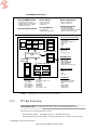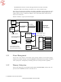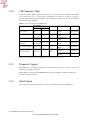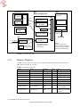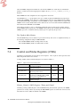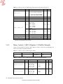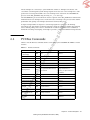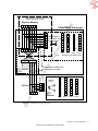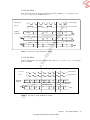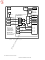
1
UltraSPARC® IIe Processor
User’s Manual
Supplement to the UltraSPARC IIi User’s Manual
Version 1.1 (Internal)
February 2003
Sun Proprietary/Confidential: Need-To-Know
Copyright © 2003 Sun Microsystems, Inc., 4150 Network Circle, Santa Clara, California 95054, U.S.A.
All rights reserved.
Sun, Sun Microsystems, the Sun logo, Netra, Ultra, Sun Blade, Netra, VIS and Sun Enterprise are
trademarks or registered trademarks of Sun Microsystems, Inc. in the U.S. and other countries.
All SPARC trademarks are used under license and are trademarks or registered trademarks of SPARC
International, Inc. in the U.S. and other countries. Products bearing SPARC trademarks are based upon
architecture developed by Sun Microsystems, Inc.
DOCUMENTATION IS PROVIDED "AS IS" AND ALL EXPRESS OR IMPLIED CONDITIONS,
REPRESENTATIONS AND WARRANTIES, INCLUDING ANY IMPLIED WARRANTY OF
MERCHANTABILITY, FITNESS FOR A PARTICULAR PURPOSE OR NON-INFRINGEMENT, ARE
DISCLAIMED, EXCEPT TO THE EXTENT THAT SUCH DISCLAIMERS ARE HELD TO BE
LEGALLY INVALID.
Table of Contents
Table of Contents i
List of Figures iii
List of Tables v
Preface vii
1. UltraSPARC IIe Processor Overview . . . . . . . . . . . . . . . . . . . . . . . . . . . . . . . . 1
1.1
1.2
1.3
1.4
UltraSPARC IIe Processor Implementation . . . . . . . . . . . . . . . . . . . . . . . . . . . . . . . . . 2
Processor Architecture . . . . . . . . . . . . . . . . . . . . . . . . . . . . . . . . . . . . . . . . . . . . . . . . . . 3
System Perspective . . . . . . . . . . . . . . . . . . . . . . . . . . . . . . . . . . . . . . . . . . . . . . . . . . . . 5
Software Perspective . . . . . . . . . . . . . . . . . . . . . . . . . . . . . . . . . . . . . . . . . . . . . . . . . . . 8
2. Clocks, System Timer, GPO, and Resets. . . . . . . . . . . . . . . . . . . . . . . . . . . . . 11
2.1
2.2
2.3
2.4
2.5
Clocks. . . . . . . . . . . . . . . . . . . . . . . . . . . . . . . . . . . . . . . . . . . . . . . . . . . . . . . . . . . . . . 11
Clock Frequency Control . . . . . . . . . . . . . . . . . . . . . . . . . . . . . . . . . . . . . . . . . . . . . . . 13
System Interrupt Timer . . . . . . . . . . . . . . . . . . . . . . . . . . . . . . . . . . . . . . . . . . . . . . . . 15
General Purpose Outputs (GPO) . . . . . . . . . . . . . . . . . . . . . . . . . . . . . . . . . . . . . . . . . 16
Resets . . . . . . . . . . . . . . . . . . . . . . . . . . . . . . . . . . . . . . . . . . . . . . . . . . . . . . . . . . . . . . 16
3. Level 2 Cache Subsystem . . . . . . . . . . . . . . . . . . . . . . . . . . . . . . . . . . . . . . . . 19
3.1
3.2
3.3
3.4
3.5
3.6
3.7
3.8
3.9
Level 2 Cache Features . . . . . . . . . . . . . . . . . . . . . . . . . . . . . . . . . . . . . . . . . . . . . . . . 19
Architecture . . . . . . . . . . . . . . . . . . . . . . . . . . . . . . . . . . . . . . . . . . . . . . . . . . . . . . . . . 20
Cache Operating Modes. . . . . . . . . . . . . . . . . . . . . . . . . . . . . . . . . . . . . . . . . . . . . . . . 23
Memory Requests . . . . . . . . . . . . . . . . . . . . . . . . . . . . . . . . . . . . . . . . . . . . . . . . . . . . 25
Level 2 Cache Operating Modes . . . . . . . . . . . . . . . . . . . . . . . . . . . . . . . . . . . . . . . . . 27
Level 2 Cache Control Bits . . . . . . . . . . . . . . . . . . . . . . . . . . . . . . . . . . . . . . . . . . . . . 29
Level 2 Cache Flush Procedure - Programming Guide . . . . . . . . . . . . . . . . . . . . . . . . 31
Level 2 Cache Initialization - Programming Guide . . . . . . . . . . . . . . . . . . . . . . . . . . . 32
Level 2 Cache Control and Status Registers (CSRs) . . . . . . . . . . . . . . . . . . . . . . . . . . 32
4. Memory Address Space . . . . . . . . . . . . . . . . . . . . . . . . . . . . . . . . . . . . . . . . . . 37
4.1
Memory Interface Unit (MIU) . . . . . . . . . . . . . . . . . . . . . . . . . . . . . . . . . . . . . . . . . . . 37
Table of Contents − i
Sun Proprietary/Confidential: Internal Use Only
4.2
4.3
SDRAM Memory Control Unit (MCU). . . . . . . . . . . . . . . . . . . . . . . . . . . . . . . . . . . . 39
Memory Space . . . . . . . . . . . . . . . . . . . . . . . . . . . . . . . . . . . . . . . . . . . . . . . . . . . . . . . 39
5. Memory Control Unit (MCU) . . . . . . . . . . . . . . . . . . . . . . . . . . . . . . . . . . . . . 43
5.1
5.2
5.3
5.4
5.5
SDRAMs and DIMMs . . . . . . . . . . . . . . . . . . . . . . . . . . . . . . . . . . . . . . . . . . . . . . . . . 43
SDRAM Command Set . . . . . . . . . . . . . . . . . . . . . . . . . . . . . . . . . . . . . . . . . . . . . . . . 44
DIMM Configuration . . . . . . . . . . . . . . . . . . . . . . . . . . . . . . . . . . . . . . . . . . . . . . . . . . 45
Control and Status Registers (CSRs) . . . . . . . . . . . . . . . . . . . . . . . . . . . . . . . . . . . . . . 46
Physical Address Mapping of DIMMs. . . . . . . . . . . . . . . . . . . . . . . . . . . . . . . . . . . . . 51
6. PCI Bus Subsystem . . . . . . . . . . . . . . . . . . . . . . . . . . . . . . . . . . . . . . . . . . . . . 55
6.1
6.2
6.3
6.4
6.5
6.6
6.7
6.8
6.9
6.10
6.11
Overview . . . . . . . . . . . . . . . . . . . . . . . . . . . . . . . . . . . . . . . . . . . . . . . . . . . . . . . . . . . 55
PCI Bus Subsystem Functional Units . . . . . . . . . . . . . . . . . . . . . . . . . . . . . . . . . . . . . 57
PIO Transactions . . . . . . . . . . . . . . . . . . . . . . . . . . . . . . . . . . . . . . . . . . . . . . . . . . . . . 60
DMA Transactions . . . . . . . . . . . . . . . . . . . . . . . . . . . . . . . . . . . . . . . . . . . . . . . . . . . . 60
PCI Bus Interface . . . . . . . . . . . . . . . . . . . . . . . . . . . . . . . . . . . . . . . . . . . . . . . . . . . . . 62
PCI Bus Commands . . . . . . . . . . . . . . . . . . . . . . . . . . . . . . . . . . . . . . . . . . . . . . . . . . . 63
PCI Bus Protocol Features . . . . . . . . . . . . . . . . . . . . . . . . . . . . . . . . . . . . . . . . . . . . . . 64
PCI Bus Arbitration . . . . . . . . . . . . . . . . . . . . . . . . . . . . . . . . . . . . . . . . . . . . . . . . . . . 67
PCI Bus Error Conditions . . . . . . . . . . . . . . . . . . . . . . . . . . . . . . . . . . . . . . . . . . . . . . 67
Processor Boot ROM . . . . . . . . . . . . . . . . . . . . . . . . . . . . . . . . . . . . . . . . . . . . . . . . . . 68
Endian Support . . . . . . . . . . . . . . . . . . . . . . . . . . . . . . . . . . . . . . . . . . . . . . . . . . . . . . . 69
7. INT_NUM Bus Interface . . . . . . . . . . . . . . . . . . . . . . . . . . . . . . . . . . . . . . . . . 73
7.1
7.2
7.3
Supported INO Values . . . . . . . . . . . . . . . . . . . . . . . . . . . . . . . . . . . . . . . . . . . . . . . . . 73
Bus Protocol . . . . . . . . . . . . . . . . . . . . . . . . . . . . . . . . . . . . . . . . . . . . . . . . . . . . . . . . . 74
Bus Protocol Examples . . . . . . . . . . . . . . . . . . . . . . . . . . . . . . . . . . . . . . . . . . . . . . . . 74
8. Clocks, Resets and MCU Initialization Content . . . . . . . . . . . . . . . . . . . . . . . 77
8.1
8.2
Clocks. . . . . . . . . . . . . . . . . . . . . . . . . . . . . . . . . . . . . . . . . . . . . . . . . . . . . . . . . . . . . . 77
MCU Power-Up Operation and Register Initialization Programming. . . . . . . . . . . . . 83
ii − UltraSPARC IIe Processor User’s Manual
Sun Proprietary/Confidential: Internal Use Only
List of Figures
FIGURE 1-1
FIGURE 1-2
FIGURE 2-1
FIGURE 2-2
FIGURE 2-3
FIGURE 2-4
FIGURE 3-1
FIGURE 3-2
FIGURE 3-3
FIGURE 3-4
FIGURE 3-5
FIGURE 3-6
FIGURE 3-7
FIGURE 3-8
FIGURE 3-9
FIGURE 3-10
FIGURE 4-1
FIGURE 4-2
FIGURE 5-1
FIGURE 6-1
FIGURE 6-2
FIGURE 6-3
FIGURE 6-4
FIGURE 6-5
FIGURE 7-1
FIGURE 7-2
FIGURE 8-1
FIGURE 8-2
FIGURE 8-3
FIGURE 8-4
Simplified Processor Block Diagram and I/O Signals . . . . . . . . . . . . . . . . . . . . . . 4
Typical System Block Diagram . . . . . . . . . . . . . . . . . . . . . . . . . . . . . . . . . . . . . . . 6
Clocks Block Diagram . . . . . . . . . . . . . . . . . . . . . . . . . . . . . . . . . . . . . . . . . . . . . 11
Power Management State Transitions Driven by Software . . . . . . . . . . . . . . . . . 14
Energy Star Register Data Field . . . . . . . . . . . . . . . . . . . . . . . . . . . . . . . . . . . . . . 14
General Purpose Outputs Data Field. . . . . . . . . . . . . . . . . . . . . . . . . . . . . . . . . . . 16
Subsystem Interfaces Block Diagram. . . . . . . . . . . . . . . . . . . . . . . . . . . . . . . . . . 21
Physical Address, Cache Line, and Register Formats . . . . . . . . . . . . . . . . . . . . . 23
RAM Array Configurations for 4-Way and Direct-Mapped Modes . . . . . . . . . . 24
Direct-Mapped Cache Mode. . . . . . . . . . . . . . . . . . . . . . . . . . . . . . . . . . . . . . . . . 27
4-Way Set-Associative Cache Mode - Tag RAM Operation . . . . . . . . . . . . . . . . 28
4-Way Set-Associative Cache Mode - Data RAM Access. . . . . . . . . . . . . . . . . . 29
UPA_Config Data Field . . . . . . . . . . . . . . . . . . . . . . . . . . . . . . . . . . . . . . . . . . . . 29
Level 2 Cache Diagnostics Addressing . . . . . . . . . . . . . . . . . . . . . . . . . . . . . . . . 33
Level 2 Cache Tag RAM Diagnostic Register Formats . . . . . . . . . . . . . . . . . . . . 34
Level 2 Cache Data RAM Diagnostic Register Formats . . . . . . . . . . . . . . . . . . . 35
Memory Request Paths . . . . . . . . . . . . . . . . . . . . . . . . . . . . . . . . . . . . . . . . . . . . . 38
MCU Memory Requests . . . . . . . . . . . . . . . . . . . . . . . . . . . . . . . . . . . . . . . . . . . . 38
Example Address Field Using 128 Mb SDRAMs on Double-Banked DIMM . . 53
Simplified Processor Block Diagram . . . . . . . . . . . . . . . . . . . . . . . . . . . . . . . . . . 56
PCI Bus Subsystem Block Diagram . . . . . . . . . . . . . . . . . . . . . . . . . . . . . . . . . . . 58
DMA Address Translations from PCI to Main Processor Memory . . . . . . . . . . . 61
Endian Byte Swapping Datapaths. . . . . . . . . . . . . . . . . . . . . . . . . . . . . . . . . . . . . 71
ROM Instruction Fetch Datapath . . . . . . . . . . . . . . . . . . . . . . . . . . . . . . . . . . . . . 72
INO Packets on INT_NUM Bus in 1x Mode . . . . . . . . . . . . . . . . . . . . . . . . . . . . 75
INO Packets on INT_NUM Bus in 2x Mode . . . . . . . . . . . . . . . . . . . . . . . . . . . . 75
Simplified Reset Block Diagram . . . . . . . . . . . . . . . . . . . . . . . . . . . . . . . . . . . . . 80
Processor Hard Reset Timing Waveforms . . . . . . . . . . . . . . . . . . . . . . . . . . . . . . 81
Processor Soft Reset Timing Diagram . . . . . . . . . . . . . . . . . . . . . . . . . . . . . . . . . 82
Avoid Test Reset Mode . . . . . . . . . . . . . . . . . . . . . . . . . . . . . . . . . . . . . . . . . . . . 83
List of Figures
Sun Proprietary/Confidential: Internal Use Only
− iii
iv − UltraSPARC IIe Processor User’s Manual
Sun Proprietary/Confidential: Internal Use Only
List of Tables
TABLE 0-1
TABLE 1-1
TABLE 2-1
TABLE 2-2
TABLE 2-4
TABLE 2-3
TABLE 3-1
TABLE 3-2
TABLE 3-3
TABLE 3-4
TABLE 4-1
TABLE 4-2
TABLE 4-3
TABLE 4-4
TABLE 5-1
TABLE 5-2
TABLE 5-3
TABLE 5-4
TABLE 5-5
TABLE 5-6
TABLE 5-7
TABLE 5-8
TABLE 5-9
TABLE 5-10
TABLE 5-11
TABLE 5-12
TABLE 5-13
TABLE 5-14
TABLE 5-15
TABLE 5-16
TABLE 6-1
TABLE 6-2
TABLE 6-3
TABLE 7-1
TABLE 8-1
Documentation List. . . . . . . . . . . . . . . . . . . . . . . . . . . . . . . . . . . . . . . . . . . . . . . viii
Processor Implementation Comparison . . . . . . . . . . . . . . . . . . . . . . . . . . . . . . . . . 2
Energy Star Register Data Field . . . . . . . . . . . . . . . . . . . . . . . . . . . . . . . . . . . . . . 15
STICK Register. . . . . . . . . . . . . . . . . . . . . . . . . . . . . . . . . . . . . . . . . . . . . . . . . . . 15
General Purpose Outputs Register . . . . . . . . . . . . . . . . . . . . . . . . . . . . . . . . . . . . 16
STICK Compare Register . . . . . . . . . . . . . . . . . . . . . . . . . . . . . . . . . . . . . . . . . . . 16
Level 2 Cache Related CSR Registers . . . . . . . . . . . . . . . . . . . . . . . . . . . . . . . . . 22
UPA_Config Register Data Fields . . . . . . . . . . . . . . . . . . . . . . . . . . . . . . . . . . . . 30
L2-Cache Tag RAM Diagnostics Data Field . . . . . . . . . . . . . . . . . . . . . . . . . . . . 35
Level 2 Cache Asynchronous Fault Status Register (AFSR) Addendum. . . . . . . 36
Accessible Memory Space . . . . . . . . . . . . . . . . . . . . . . . . . . . . . . . . . . . . . . . . . . 39
Physical Address Space . . . . . . . . . . . . . . . . . . . . . . . . . . . . . . . . . . . . . . . . . . . . 40
I/O Subsystem Address Map . . . . . . . . . . . . . . . . . . . . . . . . . . . . . . . . . . . . . . . . 41
Processor Subsystems Memory Mapped CSRs . . . . . . . . . . . . . . . . . . . . . . . . . . 41
SDRAM Memory Commands Supported. . . . . . . . . . . . . . . . . . . . . . . . . . . . . . . 44
MRS Field. . . . . . . . . . . . . . . . . . . . . . . . . . . . . . . . . . . . . . . . . . . . . . . . . . . . . . . 45
MCU Control and Status Registers. . . . . . . . . . . . . . . . . . . . . . . . . . . . . . . . . . . . 46
Memory_Control_0 (MC0) Register . . . . . . . . . . . . . . . . . . . . . . . . . . . . . . . . . . 47
Memory_Control_0 (MC0) Register Bit Definitions . . . . . . . . . . . . . . . . . . . . . . 47
Memory_Control_1 (MC1) Register . . . . . . . . . . . . . . . . . . . . . . . . . . . . . . . . . . 48
Memory_Control_1 (MC1) Register Bit Definitions: DIMM Chip Select . . . . . 48
MC1 DIMM Chip Select Base Address . . . . . . . . . . . . . . . . . . . . . . . . . . . . . . . . 49
MC1 DIMM Chip Select Base Address - Examples . . . . . . . . . . . . . . . . . . . . . . 49
Memory_Control_2 (MC2) Register . . . . . . . . . . . . . . . . . . . . . . . . . . . . . . . . . . 49
Memory_Control_2 (MC2) Register Bit Definitions: Miscellaneous . . . . . . . . . 49
Memory_Control_3 (MC3) Register Address . . . . . . . . . . . . . . . . . . . . . . . . . . . 50
Memory_Control_3 (MC3) Register Bit Definitions: I/O Buffer Strength . . . . . 50
SDRAM Row/Column Address Multiplexing . . . . . . . . . . . . . . . . . . . . . . . . . . . 52
Address Bit Usage. . . . . . . . . . . . . . . . . . . . . . . . . . . . . . . . . . . . . . . . . . . . . . . . . 52
SDRAM Parameters for DIMM Configurations. . . . . . . . . . . . . . . . . . . . . . . . . . 53
PCI Bus Commands . . . . . . . . . . . . . . . . . . . . . . . . . . . . . . . . . . . . . . . . . . . . . . . 63
PCI Bus Protocol Features . . . . . . . . . . . . . . . . . . . . . . . . . . . . . . . . . . . . . . . . . . 64
PCI Bus Error Conditions . . . . . . . . . . . . . . . . . . . . . . . . . . . . . . . . . . . . . . . . . . . 67
Incompatible INO Values When Using IChip2 . . . . . . . . . . . . . . . . . . . . . . . . . . 73
Effects of Hard and Soft Resets . . . . . . . . . . . . . . . . . . . . . . . . . . . . . . . . . . . . . . 77
List of Tables − v
Sun Proprietary/Confidential: Internal Use Only
TABLE 8-2
TABLE 8-3
Reset Sources and Effects . . . . . . . . . . . . . . . . . . . . . . . . . . . . . . . . . . . . . . . . . . . 79
Reset Propagation Times. . . . . . . . . . . . . . . . . . . . . . . . . . . . . . . . . . . . . . . . . . . . 82
vi − UltraSPARC IIe Processor User’s Manual
Sun Proprietary/Confidential: Internal Use Only
Preface
The UltraSPARC® IIe processor manual contains information about the architecture and programming
of the UltraSPARC IIe processor. It describes the details of the processor’s new features.
The UltraSPARC IIe processor is part of Sun Microsystems’ UltraSPARC II Processor family, an
enhanced 64-bit, SPARC V9 architecture implementation. The UltraSPARC IIe processor includes an
SDRAM memory controller that supports SDRAM DIMMs and a 32-bit, 66 MHz PCI bus interface,
compatible with the PCI Specification, Version 2.1. The processor integrates a 256 KB L2-cache onto
the chip, includes a clock frequency controller and new STICK timer, and operates at a lower processor
core voltage than previous processors.
SPARC V9 Architecture Manual
The SPARC Architecture Manual, Version 9 defines the processor architecture and is available from
many technical bookstores or directly from its copyright holder:
SPARC International, Inc., 535 Middlefield Road, Suite 210
Menlo Park, CA 94025, (415) 321-8692
The SPARC Architecture Manual, Version 9 provides a complete description of the SPARC V9
architecture. Since SPARC V9 is an open architecture, many of the implementation decisions have been
left to the manufacturers of SPARC-compliant processors. These “implementation dependencies” are
introduced in The SPARC Architecture Manual, Version 9.
UltraSPARC IIi User’s Manual
Since the UltraSPARC IIe processor is very similar to the UltraSPARC IIi processor, the UltraSPARC IIi
User’s Manual is a necessary companion to UltraSPARC IIe User’s Manual Supplement.
UltraSPARC I/II User’s Manual
The original UltraSPARC IIs-series processor is described in the UltraSPARC I/II User’s Manual. In
some cases, this manual may provide additional information concerning the operation of the processor.
Normally, the UltraSPARC IIi User’s Manual is sufficient as a supplement.
Other UltraSPARC User’s Manuals
All other processor UltraSPARC II User Manuals may be helpful.
Preface − vii
Sun Proprietary/Confidential: Internal Use Only
Textual Conventions
Font Usage:
•
•
•
Italic font is used for emphasis, book titles, and the first instance of a word that is defined. Italics are
also used for Assembly Language terms.
Courier font is used for register fields (named bits), instruction fields, signals, and read-only
register fields. Courier is also used for literals, instruction names, and software examples.
Bold font is used for emphasis.
•
UPPERCASE items are acronyms, instruction names, or writable register fields, and external signals.
Note: Names of some instructions contain both uppercase and lowercase letters.
•
Underbar character (_) joins words together in registers, register fields, and signal names.
Notation:
•
Square brackets ‘[ ]’ indicate the bits of a register field or external signal name.
•
Angle brackets ‘< >’ indicate a textual substitution.
•
h7’03C indicates first 7 least significant bits in the hex number 03C are relevant.
Examples:
•
SIGNAL_NAME, BUS_SIGNALS[31:0], ACTIVE_LOW_SIGNAL_L
•
Register_Bit_Field, Range_Of_Bits[3:0]
•
<enter_filename>, Emphasis
•
BERR bit
Where to Find Things
The following table can be used to find discussions about the UltraSPARC IIe processor.
The UltraSPARC II processor User’s Manual includes the UltraSPARC IIi User’s Manual and the
UltraSPARC I/II User’s Manual.
TABLE 0-1
Documentation List
Document
Item
Name
Chapter/Section
Reference
Architecture, Operation, and CSRs of
processor/MMU
User’s Manual
UltraSPARC II
Architecture, Operation, and CSRs of
L1-caches
User’s Manual
UltraSPARC II
Architecture, Operation, and CSRs of
L2-caches
User’s Manual
UltraSPARC IIe
viii − UltraSPARC IIe Processor User’s Manual
Sun Proprietary/Confidential: Internal Use Only
Chapter 3, Level 2 Cache Subsystem,
page 19
TABLE 0-1
Documentation List (Continued)
Document
Item
Name
Chapter/Section
Reference
Architecture, Operation, and CSRs of
Memory Controller
User’s Manual
UltraSPARC IIe
Architecture, Operation, & CSRs of PCI
Subsystem
User’s Manual
UltraSPARC IIi
Clock Operations
User’s Manual
UltraSPARC IIe Section 2.1, Clocks, on page 11
Errata upto UltraSPARC IIi
User’s Manual
UltraSPARC II
Glossary
User’s Manual
UltraSPARC II
Interrupts and Traps
User’s Manual
UltraSPARC II
Memory ASI Definitions
User’s Manual
UltraSPARC II
Memory Transaction Ordering
User’s Manual
UltraSPARC II
Power Management Energy Star (E-Star)
Operation
User’s Manual
UltraSPARC IIe
Programming Code Generation Guidelines
User’s Manual
UltraSPARC II
Programming Grouping Rules and Stalls
User’s Manual
UltraSPARC II
System Memory Map
User’s Manual
UltraSPARC IIe Section 4.3, Memory Space, on page 39
Chapter 5, Memory Control Unit
(MCU), page 43
UltraSPARC IIi User’s Manual,
Chapter 19
UltraSPARC IIi User’s Manual,,
Appendix K
UltraSPARC IIi User’s Manual,,
Chapter 11
UltraSPARC IIi User’s Manual,,
Chapter 6 and this document
Section 2.2, Clock Frequency Control,
on page 13
UltraSPARC IIi User’s Manual,,
Chapter 21
UltraSPARC IIi User’s Manual,,
Chapter 22
Preface − ix
Sun Proprietary/Confidential: Internal Use Only
x − UltraSPARC IIe Processor User’s Manual
Sun Proprietary/Confidential: Internal Use Only
CHAPTER
1
UltraSPARC IIe Processor Overview
The UltraSPARC IIe processor integrates a 256 KB L2-cache, an SDRAM memory controller, a 66 MHz
32-bit PCI Bus Interface, and a power management feature. The processor is very similar to all other
UltraSPARC II processors. It implements the 64-bit SPARC V9 architecture and the VISTM instruction
set. The SPARC V9 architecture provides binary compatibility across all SPARC processors. The VIS
instruction set performs parallel execution on multiple pixel data widths of 8 and 16 bits to accelerate
the most common operations related to processing, 2D and 3D graphics, compression algorithms, and
numerous network operations. The VIS instruction set enables high bandwidth for memory-to-processor
and memory-to-memory transfers by providing 64-byte block load and block store operations.
Integrated Features
The SDRAM DIMM memory controller supports up to 2 GB of memory using four double-sided,
512 MB DIMMs with 128 Mb SDRAMs or four single sided, 512 MB DIMMs with 256 Mb SDRAMs.
The PCI Bus subsystem provides command and data buffering, and an I/O memory management unit
(IOM) for PCI bus masters accessing main memory. The processor’s host bus interface is PCI Bus 2.1
compatible, 32 bits wide, operates at up to 66 MHz, sends and receives 3.3 V signals, and is often
connected to Sun’s Advanced PCI Bridge (APB). The APB extends the PCI Bus structure to include two
additional bus segments of 32 bits at 33 MHz with 3.3 or 5.0 V signaling.
The fully integrated L2-cache contains up to 256 KB of space for instructions and data. The L2-cache
allocates space in 4-way set-associative and direct-mapped mode.
Power Management Logic provides a mechanism to slow down the processor clock rate. This reduces
power consumption while running the operating system.
The JTAG interface supports boundary scan for systemboard interconnect testing.
Each functional area on the UltraSPARC IIe processor maintains decentralized control, allowing many
activities to overlap.
Chapter 1 • UltraSPARC IIe Processor Overview − 1
Sun Proprietary/Confidential: Internal Use Only
1.1
UltraSPARC IIe Processor Implementation
1.1.1
New Features
The following list of items are features in the UltraSPARC IIe processor that are not necessarily found
in previous UltraSPARC processors (s-series and II), but will impact the system software and some of
the application software.
•
•
•
•
•
•
1.1.2
Memory Controller (SDRAM) − New, impacts initialization code (firmware)
Clock Control Unit (1/2 and 1/6 frequency modes) − New, enables Energy Star (E-Star) mode
STICK Timer − New, impacts Operating System (OS) time base when E-Star mode is used
Traps − Minor software changes for the STICK timer support
L2-cache − New internal 256 KB cache replaces external L2-cache. New cache flushing method
required, no other impact to software code
Four General Purpose Output (GPO) signals − New, available for PCI clock control or other
functions
Features Removed
The following list of items are not supported in the UltraSPARC IIe processor that were supported in
previous UltraSPARC processors.
•
•
•
1.1.3
UPA Bus (all port types, including UPA64S)
External tag and data L2-cache SRAMs (replaced by internal cache RAM arrays)
EDO DRAM memory controller (replaced by SDRAM memory controller)
Processor Comparison
All processors listed below include the UltraSPARC II pipeline and the VIS instruction set. The MMU
and L1-caches structures are very similar. TABLE 1-1 shows a comparison of processor implementations.
TABLE 1-1
Processor Implementation Comparison
UltraSPARC IIs-series
UltraSPARC IIi
UltraSPARC IIe
Sun Platforms
Ultra 10, Ultra 20,
UltraTM 1, Ultra 2,
Sun EnterpriseTM Servers UltraAXi
Sun BladeTM 100,
NetraTM t1120, t1125,
t1400, t1405,
CP2060, CP2080,
AX1105
Year of first system
1996
1998
2000
Clock Frequency
167 to 480 MHz
270 to 440 MHz
400, 500 MHz
Process Technology
0.35 and 0.25 µm Al
0.35 and 0.25 µm Al
0.18 µm Al
System Bus
UPA64M (up to 64-way)
UPA64S (graphics only)
I/O Bus
S-bus and PCI bus via
UPA system bridge
PCI 66 MHB, 32-bit
Memory Bus
EDO DRAM
EDO DRAM
2 − UltraSPARC IIe Processor User’s Manual
Sun Proprietary/Confidential: Internal Use Only
PCI
SDRAM
TABLE 1-1
Processor Implementation Comparison (Continued)
UltraSPARC IIs-series
Maximum Memory
1.2
UltraSPARC IIi
UltraSPARC IIe
1 GB
2 GB
L2-cache
1 to 8 MB, external,
module dependent
256 KB to 1 MB, external, 256 KB On-Chip,
module dependent
4-way Set-Associative
Energy Star Mode
No
No
1/2 and 1/6
Processor Architecture
The UltraSPARC IIe processor consists of six major components. The components are listed with their
interconnections in FIGURE 1-1.
The central compute engine and primary caches in the UltraSPARC IIe processor provides very similar
functionality as all other UltraSPARC II processors. The UltraSPARC IIe processor has integrated
features to further reduce systemboard size, board cost, and power dissipation.
1.2.1
Processor/MMU/Primary Level 1 Caches
Compatibility Note – The primary level 1 caches are the same as all other UltraSPARC II
processors, with an enhancement for trap generation to serve the new STICK timer.
Documentation Note – See the other UltraSPARC II processor manuals for the description of the
processor, MMU, and primary caches.
1.2.2
Integrated Level 2 Cache
•
•
1.2.3
Secondary Cache (L2-Cache) − Unified Instruction-Data Memory, 256 KB, 4-way set-associative or
direct-mapped mode
Cache Control Unit (ECU) − Interfaces the L2-cache to the processor, Memory, and PCI subsystems
SDRAM Memory Subsystem
•
•
Memory Interface Unit (MIU) − Accepts, buffers, checks for data coherency, and arbitrates memory
requests
SDRAM Memory Control Unit (MCU) − 72-bit interface
Chapter 1 • UltraSPARC IIe Processor Overview − 3
Sun Proprietary/Confidential: Internal Use Only
UltraSPARC IIe Processor
processor/MMU/Caches
•
•
•
•
Clocks, Resets
• Clock Control Unit
• Energy Star Logic
• Reset Logic
Integer Execution Unit (IEU)
Floating Point Unit / VIS Execution
Prefetch and Decode Unit (PDU)
Load/Store Unit (LSU)
• Tag RAM Array
• Data RAM Array (256 KB)
processor/MMU/
Clocks, Resets
D-Cache
PDU
LSU
• Memory Interface Unit
• Memory Control Unit
PCI Bus Subsystem
L2-cache Memory
Cache Control Unit (ECU)
I-Cache
Memory Subsystem
MMU
IEUs
CCU
FPUs
ESTAR
•
•
•
•
PCI Data Path (PDP)
PCI Bus Module (PBM)
I/O Memory Management Unit (IOM)
Resets, Interrupts, Error (PIE)
Clock, Reset, Mode Signals
•
•
•
•
•
•
CLKA & CLKB
SYS_RESET_L,
P_RESET_L, X_RESET_L
RMTV_SEL
VID
GPO
VIS
Resets
Memory Subsystem
Cache Control Unit
(ECU)
Power, Ground
•
•
•
•
Vdd_IO
Vdd_core
VDD_PLL, VDD_DIFF
VSS, VSS_PLL
MIU
SDRAM Signals
MCU
L2-cache
Memory
PCI Bus Subsystem
TAG
PDP
256
JTAG Test Signals
PBM
IOM
PCI_AD
PCI_CBE_L
PCI_FRAME_L
PCI_I/TRDY_L
PCI_REQ/GNT_L
PCI_DEVSEL_L
PCI_P/SERR_L
1.2.4
•
•
•
•
TCK
TRST_L
TMS
TDI, TDO
Test Signals
PCI Bus Signals
FIGURE 1-1
MEM_CLK/CLKE
MEM_CS/WE
MEM_RAS/CAS
MEM_ADDR/BANK
MEM_DATA/ECC
MEM_SCLK_OUT/IO_SCLK
PIE
KB
•
•
•
•
•
•
•
•
•
•
•
•
•
•
•
•
•
•
•
•
PCI_RST_L
PCI_CLK, PCI_REF_CLK
INT_NUM
SB_DRAIN
SB_EMPTY
SYNC_3TO1
PCI_STOP_L, PAR
•
•
•
•
•
•
•
PLLBYPASS, EPD
CPU_L5CLK, PCI_L5CLK
RAM_TEST, ITB_TEST
PMO
TEMP_SENSE
EXT_EVENT
OBSRV_MCU
Simplified Processor Block Diagram and I/O Signals
PCI Bus Subsystem
Compatibility Note – The PCI Bus subsystem is same as the UltraSPARC IIi processor.
The major blocks of the PCI Subsystem includes:
•
PCI Bus Module (PBM) − 33/66 MHz, 32-bit, 3.3 V PCI Host Bus Interface
•
I/O Memory Management Unit (IOM) − Translates PCI addresses to memory’s physical address
4 − UltraSPARC IIe Processor User’s Manual
Sun Proprietary/Confidential: Internal Use Only
•
PCI Data Path (PDP) − Dual 64-byte data buffer (one for PIO and one for DMA)
•
PCI Resets, Interrupts, and Error (PIE) − Εxternal interrupts processed
The PCI Subsystem is clocked independently from the processor. A 2-entry, bidirectional command
buffer is at the PCI to processor clock domain boundary to decouple activities from the processor to
improve PCI data transfer bandwidth.
1.2.5
System Control
Clocks
•
Processor Clock Input − Differential CLKA/B
•
New: Clock Control Unit (CCU) − PLL, 1/2 and 1/6 divider select
•
Internal Clock Distribution − Utilizes internal PLL to reduce on-chip clock skew
•
Memory Clock derived from CLKA/B − Programmable divider
•
PCI Clock − 66 MHz Subsystem Clock, 33/66 MHz PCI Interface Clock
Resets
•
POR, system (hardware), and XIR (software)
•
Red_State Mode Trap Address Vector Select (RMTV_SEL)
•
Test Interfaces: JTAG, Factory Tests
Diagnostics
1.3
•
Control Status Registers (CSRs) − Most processor subsystems
•
TAP Controller, JTAG − Boundary Scan
System Perspective
The UltraSPARC IIe processor interfaces directly to industry standard SDRAM DIMMs for memory.
The processor also contains a PCI 2.1 compatible bus interface for system I/O functions. These
interfaces provide a high degree of compatibility with standard design practices and device interfacing.
The entire system is memory mapped with Address Space Identifiers (ASI) that add functionality to each
load/store transaction from the processor. This expands the effective address space of the processor and
reveals special registers for system control.
Sun offers and recommends a number of system devices, including:
•
Advanced PCI Bridge (APB) that expands the UltraSPARC IIe PCI Bus Interface to two PCI Bus
segments.
•
PCIO-2 Multifunction PCI I/O controller that supports Ethernet, Sun’s 8-bit E-Bus, USB, and
IEEE1394
•
IChip2 System ASIC for I/O interrupt concentration, and PCI clocks
Older devices compatible with the UltraSPARC IIe processor includes:
Chapter 1 • UltraSPARC IIe Processor Overview − 5
Sun Proprietary/Confidential: Internal Use Only
•
PCIO Multifunction PCI I/O controller that supports Ethernet and Sun’s 8-bit E-Bus
•
RIC System ASIC for I/O interrupt concentration, reset control, and JTAG clocks
These devices provide Sun-proven hardware and software compatibility. System designers can choose
from a number of architectures based on these and standard PCI devices. Design requirements and
software efforts need to be considered in addition to device functionality when choosing the best
devices for an architecture.
FIGURE 1-2 illustrates a typical system block diagram.
Clocks
& Resets
JTAG
UltraSPARC IIe
Processor
64-bit Data
plus 8-bit ECC
SDRAM DIMMs
16 MB - 2 GB
PC-100 Compatible
RIC or
IChip
Concentrator INT_NUM
External Interrupts
Advanced PCI
Bridge (APB)
A 32-bit, 33 MHz, 3.3/5 V
B
32-bit, 33 MHz, 3.3/5 V
Primary PCI System Bus
32-bit, 33/66 MHz, 3.3 V
Boot Flash ROM
NVRAM/RTC
PCI Devices on
Primary Bus
Sun I/O
Controller
(PCIO-2)
A Sun Architecture is shown.
Other architectures are possible
using industry-standard PC devices.
FIGURE 1-2
1.3.1
Super I/O
Chip
PCI Devices on
Secondary Bus
Keyboard/Mouse
Floppy
Serial/Parallel
8-bit E-Bus
IR/USB/GPIO
Typical System Block Diagram
Power Management
The processor can be slowed to 1/2 and under certain operating conditions, 1/6 the normal operating
frequency. The memory controller can put the SDRAMs into Self Refresh mode. Software can further
reduce system power consumption by controlling system devices with power down capabilities.
1.3.2
Memory Subsystem
The processor supports up to four double-sided PC-100 style SDRAM DIMMs (8 banks, total). The
processor clock to SDRAM clock ratio is selectable (4 to 7).
6 − UltraSPARC IIe Processor User’s Manual
Sun Proprietary/Confidential: Internal Use Only
Each DIMM can have one or two physical banks and they can all be of a different address size and
configuration. Modes and timing parameters are shared across the DIMMs. The memory interface has
programmable I/O buffer strengths to adjust the DC current output drive on separate groups of signals to
optimize signal transmission integrity over various capacitive loading conditions. SDRAM memories
can be operated in Self Refresh mode to reduced power consumption.
1.3.3
PCI Bus Architecture
The PCI Bus subsystem directly interfaces the processor to a 32-bit, Version 2.1 compliant PCI Bus
running at speeds up to 66 MHz (which yields a maximum theoretical transfer rate of 264 MB/s). The
PCI Bus Arbiter can support up to four external PCI Bus Masters. The number of devices that can be
attached depends on the physical limits and the bus clock frequency. A built-in I/O Memory
Management Unit (IOM) will translate PCI memory space addressees from the PCI Bus Master to the
physical addresses of the main memory. The processor is a PCI Slave in this DMA transfer mode to and
from memory. The IOM also supports hardware tablewalk in the case of a TLB miss in the IOM. All
memory reads and writes initiated by a PCI Bus Master (DMA) are cache coherent with the processor.
The processor boots by initiating a 32-bit memory read request on the PCI Bus Interface. The
UltraSPARC IIe processor has two sets of trap vectors to be compatible with Sun and the PC boot
address modes.
Advanced PCI Bridge (APB) Chip
The APB extends the UltraSPARC IIe PCI Bus to two PCI 2.1 bus segments of 33 MHz, 32-bit each.
The APB drives to 3.3 V levels. The secondary bus segments have configurable I/O buffers to be 5 V
tolerant. The APB supports DMA from up to four bus masters on each secondary bus segment.
The APB interfaces seamlessly with the UltraSPARC IIe processor. Software is available to support the
APB and the 2115x class of PCI bridges.
System Interrupts (INT_NUM Bus)
The PCI subsystem processes I/O interrupts from the systemboard that are received on its 6-bit
INT_NUM bus. Dozens of interrupt lines are scanned, encoded or concentrated onto the INT_NUM bus
by a system ASIC containing an “Interrupt Concentrator.” The UltraSPARC IIe processor uses software
interlocks and hardware write buffer (store buffer) flushing logic to synchronize a DMA transfer to the
interrupt handler.
System interrupts are considered part of the PCI Subsystem because they service PCI devices or devices
indirectly attached to the PCI Bus.
PCIO Multifunction PCI I/O Controller
The PCI I/O controller (PCIO, STP2003QFP) chip is a multifunction PCI Controller that includes a 10/
100 Ethernet interface and an E-Bus host controller.
PCIO-2 Multifunction PCI I/O Controller (Enhanced)
The second generation PCI I/O Controller (PCIO-2, SME2300BGA) chip is a multifunction PCI
Controller that includes a 10/100 Ethernet interface, an E-Bus host controller, an IEEE 1394 Firewire
Interface, and four USB bus interfaces.
Chapter 1 • UltraSPARC IIe Processor Overview − 7
Sun Proprietary/Confidential: Internal Use Only
1.3.4
System ASICs
RIC Reset/Interrupt/Clock ASIC
The RIC System Controller (SME2210) supports the system resets, system interrupts, system scans, and
system clock control functions for UltraSPARC II s-series processors. Its features includes:
•
•
•
•
•
Resets from power supply, reset buttons, and scan chain
Interrupt Concentrator − 41 signals in, 6-bit encoded INT_NUM bus out
Directs scan inputs and outputs through scan chains
Combinational logic for UPA bus speed
160 pin PQFP
IChip2 Interrupt Controller ASIC (Enhanced)
The IChip2 System Controller (SME2212QFP) provides similar Interrupt Concentrator function as the
RIC chip. The rest of the IChip2 includes a PCI clock controller requiring a differential voltage input
signal.
•
•
•
•
Interrupt Concentrator − 48 signals in, 6-bit encoded INT_NUM bus out
PCI Clock Controller − Compatible with asynchronous dual bus structures
128-pin TQFP package
Newer device than RIC
The IChip and IChip2 controllers are functionally equivalent. The IChip System Controller is packaged
in a 120-pin MQFP.
1.4
Software Perspective
There are new ASIs for accessing the memory controller, the L2-cache RAMs, and the PCI Bus
Interface Controllers. Main memory (SDRAMs) is mapped as cacheable. All the PCI memory spaces
are non-cacheable memory mapped. This includes configuration, I/O, and memory.
Compatibility Note – The processor architecture is similar to the processor architecture of all other
UltraSPARC II processors.
The PCI Bus architecture is similar to the PCI architecture in the UltraSPARC IIi processor.
Endianess Note
The UltraSPARC IIe processor uses the big-endian addressing format. The code space and all processor
registers are big-endian except the PCI Configuration Space Header in the PCI subsystem and the PCI
Bus itself.
The processor supports little-endian data structures using a combination of the byte swapper in the PCI
Bus subsystem and the ASI descriptors of the processor.
8 − UltraSPARC IIe Processor User’s Manual
Sun Proprietary/Confidential: Internal Use Only
System Bus Hierarchy Model Note
The UltraSPARC system architecture is bus hierarchy-based. The processor’s I/O system bus is the PCI
Bus Interface. The optional Advanced PCI Bridge (APB) provides two secondary PCI Bus segments.
Sun’s PCIO-2 PCI Multifunction I/O Controller provides an interface to Ethernet, IEEE 1394, E-Bus
and USB type busses to further define the system’s bus hierarchy which originates at the processors
primary Host PCI Bus Interface.
Chapter 1 • UltraSPARC IIe Processor Overview − 9
Sun Proprietary/Confidential: Internal Use Only
10 − UltraSPARC IIe Processor User’s Manual
Sun Proprietary/Confidential: Internal Use Only
2
CHAPTER
Clocks, System Timer, GPO, and Resets
2.1
Clocks
There are three root clock domains in normal operation.
•
Processor clock (CLKA, CLKB, differential signal pair, 400/500 MHz)
•
PCI (PCI_CLK LVTTL signal, 66 MHz)
•
JTAG (JTAG_TCK LVTTL signal)
All three sets of clocks are normally asynchronous to each other. Synchronizers are used to transfer
address data, and control signals between the PCI and processor clock domains. FIGURE 2-1 illustrates a
clocks block diagram.
ESTAR_Mode[1:0]: E_Star_Mode
Mem_Control_0[30:29]: Clock_Ratio
Processor Clock
Clock Control Unit
Multiply/Divide
Logic
Clock Buffer and
Distribution Tree
CLKA
CLKB
4, 5, 6, 7
SDRAM
Clocks
TO
SDRAMs
Latch Read Data
PLL
Control
Processor Core Logic
Processor Clock Domain
TIC
Logic
PCI Clock Domain
PCI_CLK
PLL
ú12
PCI to processor
Synchronizer
en
PCI_REF_CLK
en STICK
Logic
INT level 14
INT level 14
JTAG Clock Domain
PCI Bus I/F
JTAG Logic
JTAG_CLK
FIGURE 2-1
Clocks Block Diagram
Chapter 2 • Clocks, System Timer, GPO, and Resets − 11
Sun Proprietary/Confidential: Internal Use Only
2.1.1
CLKA and CLKB Processor Clock Signal
The CLKA and CLKB clock pair are driven continuously and at a constant rate of 1/2 the processor’s
normal operating frequency.
Clock Control Unit (CCU)
The processor clock input signal on the processor is a differential signal pair. The Clock Control Unit
(CCU) converts this to a CMOS signal, uses it to drive its PLL, and operates high speed dividers to
provide three processor frequency mode settings to reduce power dissipation.
The processor clock is driven at a constant frequency by system logic and runs continuously while
operating the processor. The clock is driven at one-half the processor operating frequency in normal
operating mode. The processor frequency can be reduced to 1/2 (same frequency as input clock signal)
or 1/6 the normal operating frequency, by writing to the Energy Star (E-Star) register.
Timebase for Software − TICK and STICK
The processor contains two clock timers that can be read by software or be used to generate interrupts
at fixed intervals of time. Each timer contains a counter, a count value register, and a compare register.
The counter updates the count value register. When the count value register equals the compare register
value, an interrupt is generated. The TICK logic is incremented by the processor clock.
The STICK logic (new in the UltraSPARC IIe processor) uses the PCI clock for a constant time base.
The PCI clock provides a constant time base to the processor STICK logic when the TICK logic is
affected by the switch in processor frequency. The PCI_REF_CLK clock input must remain at a
constant rate for the STICK logic to keep good time. The system software can use the original TICK or
the new STICK logic, or a combination of both to maintain a time reference. The TICK logic is affected
by the processor operating frequency and the STICK logic is affected by the PCI clock frequency.
The operation of TICK timer is described in the UltraSPARC IIi User’s Manual.
2.1.2
Memory Clocks
The MEM_SCLK[7:0] signals are derived by dividing the processor clock by 4, 5, 6, or 7. The memory
controller is discussed in detail in Chapter 5, Memory Control Unit (MCU), page 43.
2.1.3
PCI Subsystem Clocks
The PCI_CLK clock is driven at the PCI Bus Interface frequency, typically 66 MHz or 33 MHz,
although intermediate frequencies are also supported.
The PCI_CLK clock is divided and synchronized to the processor clock for the STICK logic. The
STICK logic is read by software to maintain accurate time using the PCI clock as a time basis
(independent of power down states in a processor).
2.1.4
JTAG Clock
The JTAG clock is independent of the other two clock domains.
12 − UltraSPARC IIe Processor User’s Manual
Sun Proprietary/Confidential: Internal Use Only
2.2
Clock Frequency Control
Power Management consists of software detecting a system that has been idle for a prolonged period of
time and then lowering the processor clock frequency to 1/2 or 1/6 the normal operating mode and
optionally programming the SDRAM devices into their power down, self-refresh mode. Additional
power savings in the system I/O is possible.
2.2.1
PCI/Processor Frequency Restrictions
The processor core frequency must be at least twice the frequency of the primary PCI Bus to ensure that
the processor core correctly detects signals driven by the PCI data path inside the processor. This is
further explained in the datasheet.
This requirement makes the 1/6 mode unusable when the primary bus frequency is 66 MHz.
2.2.2
Frequency Transitions
An example of state transitions for power management are shown in FIGURE 2-2. Consider the need to
set a new auto-refresh interval with each change of processor frequency. After software changes the
processor frequency, the software should, as a precaution, execute enough NOP instructions so at least
16 processor clocks occur before any memory or PCI references take place. The PCI subsystem should
also be quiescent. There is no transition supported from 1/1 to 1/6 mode or visa-versa.
Impact of PLL Enabled DIMMs
The buffered and registered DIMM types contain PLL circuits on the DIMM to reduce clock skew.
When the processor changes frequency, the memory clock frequencies changes, too. If this happens, the
PLL enabled DIMMs lose their PLL lock causing the DIMM to be unusable until it stabilizes. Since
there is no way to block memory accesses, one may occur while the PLL is locking. If this happens
there is a chance the memory transaction gets corrupted and the system fails.
For this reason, we recommend not using the power down modes with registered and buffered DIMMs.
Use unbuffered DIMMs when power management is required.
Chapter 2 • Clocks, System Timer, GPO, and Resets − 13
Sun Proprietary/Confidential: Internal Use Only
Normal Operating
Mode
1. Set ESTAR: 1/1 Mode
2. Wait 16 processor clocks.
3. Set refresh interval.
1. Set refresh interval.
2. Set ESTAR: 1/2 Mode
3. Wait 16 processor Clocks
1/2 Frequency
No Self Refresh
1. Clear MC0: Self Refresh
2. Consider external devices
1. Consider external devices
2. Set MC0: Self Refresh
1/2 Frequency
Self Refresh
Set ESTAR: 1/6 mode
Set ESTAR: 1/2 mode
1/6 Frequency
Self Refresh
FIGURE 2-2
2.2.3
Power Management State Transitions Driven by Software
Power Management (Energy Star Register)
Power Management is controlled by writing to the E-Star register.
Note – The UltraSPARC IIe processor clocking must be kept active (1/1, 1/2, or 1/6 mode). The PCI
clock to the UltraSPARC IIe processor must remain active, but the PCI clock to the system devices can
be stopped if proper care is taken with the PCI Bus system devices. Control of the PCI clock generator
can be done by using two of the GPO signals that are driven directly by the UltraSPARC IIe processor
and controlled by software. Some of Sun’s architectures use GPO[1:0] for this purpose.
FIGURE 2-3 and TABLE 2-1 illustrates and describes the E-Star register data field, respectively.
E-Star Register Data Field
Read/write:
0x01FE.0000.F080
00000000000000000000000000000000000000000000000000000000000000
63
E-Star
2 1
FIGURE 2-3
Energy Star Register Data Field
14 − UltraSPARC IIe Processor User’s Manual
Sun Proprietary/Confidential: Internal Use Only
0
TABLE 2-1
Energy Star Register Data Field
Field
Bits
Description
Reserved
63:02
Reserved
E_Star_Mode 1:0
2.3
00: Full Operating Frequency
01: 1/2 Operating Frequency
10: 1/6 Operating Frequency
11: Reserved
POR
Type
00
R/W
Documentation
Reference
System Interrupt Timer
When the processor frequency is lowered (via E-Star modes) the time base for the TICK logic in the
processor is affected. A new STICK timer has been created that is driven at the PCI_CLK signal input
frequency rate which must remain constant for the PCI Bus Interface Clock PLL.
The System Tick (STICK) can provide a constant time base for the operating system because the
PCI_CLK must be driven at a constant rate.
The STICK has an associated compare register (STICK_CMP) to generate a periodic interrupt for the
operating system. The STICK alarm signal is gated with the TICK alarm signal. Either alarm (if
enabled) will generate a level-14 (0x4e offset) trap.
The functionality is similar to the processor Tick (TICK) and Tick Compare (TICK_CMP) logic except
it is not subject to variations in the processor clock rate.
The STICK counter is clocked by the internal processor clock, but is enabled by a pulse derived from a
constant PCI Bus clock source. This means the PCI clock must remain on and at a known constant rate
for the operating software to maintain accurate time when using STICK. Similarly the processor clock
must remain active, but can be at a reduced rate.
The PCI clock is divided by 12 and fed into a synchronizer. The synchronizer issues an enabling pulse
to the STICK counter at 1/12 the PCI Bus clock speed and does so in the processor clock domain. The
enable rate is 5.5 MHz using a 66 MHz PCI Bus. The pulse is used to enable the STICK to make one
count. The processor clock rate is 67 MHz for a 400 MHz processor in 1/6 power down mode so the
enabling pulses from the synchronizer are always detected.
When the STICK_CMP logic determines that the timer has timed out, a level-14 interrupt
(STICK_ALARM) is generated to cause a trap in the processor, same as the TICK_CMP logic, only
separate. One, both, or neither timer can be enabled. We recommend enabling one timer at a time to
simplify software.
TABLE 2-2 and TABLE 2-3 describes the STICK Register and the STICK Compare Register, respectively.
TABLE 2-2
STICK Register
Field
Reserved
Stick_Count
Bits
63
62:0
Description
POR
Type
Reads 0, No Write
0
R
STICK Register Count Value
0
R/W
Chapter 2 • Clocks, System Timer, GPO, and Resets − 15
Sun Proprietary/Confidential: Internal Use Only
TABLE 2-3
STICK Compare Register
Field
Bits
63
Stick_Alarm_Enable
62:0
Stick_Compare_Value
2.4
Description
POR
Type
0 = Enable Stick Alarm (Int 14h)
1 = Disable Stick Alarm
0
R
Field is compared to Stick_Count. If
alarm is enabled and count matches, then
Int 14h is asserted.
0
R/W
General Purpose Outputs (GPO)
The UltraSPARC IIe processor has four general purpose output signals that come directly from the
processor and are controlled by software writable registers. Two of these outputs are designated by Sun
software for PCI clock control, but can otherwise be used for any purpose.
For software controlled output signals, set to 1 to drive output to 3.3 V. Set to 0 to drive output to 0 V.
Output is clocked by CLKA/CLKB.
FIGURE 2-4 and TABLE 2-4 illustrates and describes the general purpose outputs data field and register,
respectively.
General Purpose Output (GPO) Data Field
Note: Bits [63:4] are not physically implemented.
These bits return zero when accessed.
GPO3 GPO2
0000000000000000000000000000000000000000000000000000000000000000
63
2.5
4
FIGURE 2-4
General Purpose Outputs Data Field
TABLE 2-4
General Purpose Outputs Register
3
2
GPO1 GPO0
1
Field
Bits
Description
POR
Type
Reserved
63:4
Reads 0, No Write
0
RO
GPO3
3
Controls state of GP3 signal
1
R/W
GPO2
2
Controls state of GP2 signal
1
R/W
GPO1
1
Controls state of GP1 signal
1
R/W
GPO0
0
Controls state of GP0 signal
1
R/W
0
Resets
The processor has two groups of resets − power-on and system resets, and software resets. The
power-on and system resets affect the entire processor and PCI Bus subsystem. A software reset simply
causes a processor trap. In each case, the cause of the reset is recorded in the Reset Control (RC)
register, the processor is put into its RED_State condition, and the processor code execution jumps to
non-cacheable ROM memory space.
16 − UltraSPARC IIe Processor User’s Manual
Sun Proprietary/Confidential: Internal Use Only
The Reset Control (RC) register contains bits to enable software to generate soft resets and to record the
highest level reset which the processor is responding to and recovering from.
Documentation Note – All of the Processor Reset information in this section is provided as an
overview. The operation of resets has not changed significantly from that of the UltraSPARC IIi
processor. The manual for this processor provides an additional source of information about processor
resets.
POR Reset (Hardware Reset)
The POR Reset is a hard reset that resets the processor and PCI Bus subsystem. The POR Reset is
caused by the assertion of the SYS_RESET_L signal pin, the P_RESET_L signal pin, or by writing to
the Soft_POR bit in the Reset Control Register. The POR Reset affects most of the processor and
propagates out to the PCI_RST_L signal pin to reset the PCI Bus subsystem.
The POR Reset causes the processor to immediately stop its current activity. The de-assertion of reset
allows a sequence of events to occur. During this sequence, the hardware is initialized, the processor is
put in its RED_State condition, the PCI_RST_L signal is released, and the processor begins
instruction execution to ROM memory space.
Chapter 2 • Clocks, System Timer, GPO, and Resets − 17
Sun Proprietary/Confidential: Internal Use Only
18 − UltraSPARC IIe Processor User’s Manual
Sun Proprietary/Confidential: Internal Use Only
3
CHAPTER
Level 2 Cache Subsystem
The Level 2 Cache (L2-cache) subsystem includes the L2-tag and L2-data memory arrays and various
Control, Status, and Diagnostic registers (CSRs). The L2-cache responds to the commands of the
“ECU.” The ECU manages the flow of the data and control signals and is driven by memory requests
and the cache states.
The ECU controls write buffers and monitors the addresses they contain in order to maintain data
coherency with the caches and main memory. The ECU interfaces to the PCI subsystem to support DMA
transfer requests from the PCI Bus into the coherent data domain of the processor memory.
The L2-cache memory is physically indexed and physically tagged. The cache line size in the L2-cache
and main memory is 64 bytes. The L2-cache can operate in 4-way set-associative mode, or
direct-mapped mode. The purpose of having two modes is to provide flexibility in operation for
performance considerations (4-way), predictable behavior (direct-mapped), and to flush the cache of
modified data (direct-mapped).
The L2-cache operates in a write-back mode. The primary I-cache and D-cache operate in write-through
mode.
Compatibility Note – The UltraSPARC IIe processor includes the L2-cache tag and Data RAM
arrays. Previous processors, like the UltraSPARC IIi processor, contain a cache controller that interfaces
to external tag and Data SRAMs. In addition, the L2-cache in the UltraSPARC IIe processor is enhanced
with a 4-way set-associative operating mode.
Documentation Note – The UltraSPARC IIi Processor User’s Manual contains information for the
processor, MMU, I-cache/PDU, D-cache/LSU, the cache controller (ECU), and the PCI Bus subsystem.
Since the operation of the UltraSPARC IIe processor is nearly identical to the UltraSPARC IIi processor
for these functions, please refer to the UltraSPARC IIi Processor User’s Manual. The L2-cache in the
UltraSPARC IIe processor is unique and not found on other processors.
3.1
Level 2 Cache Features
•
256 KB of Data Storage
■
■
■
Cache address space − PA[30:0] = 2 GB
Line Entry − 64-byte (8 data transfers)
Diagnostic Organization − 8192 64-bit data words per bank × 4 banks
Chapter 3 • Level 2 Cache Subsystem − 19
Sun Proprietary/Confidential: Internal Use Only
•
Tag RAM Array:
■
■
•
Line Entry − 15-bit tag + 2-bit status + 2-bit parity (single transfer)
Organization − 1024 cache line entries per bank × 4 physical banks × 20 bits
Line Replacement Selection RAM Array (Rand Array):
■
■
■
Usage − 4-way set-associative mode only
Line Entry − 2-bit random replacement number (Rand)
Organization − 1024 cache line entries per bank × 4 banks × 64-byte cache line
Performance Features
The L2-cache is pipelined and operates in the 2-2 mode as defined by previous UltraSPARC products.
This enables the L2-cache to sustain the bandwidth of one 64-bit data transfers every two processor
clocks from the Data RAM array. The 64-bit datapath width exists throughout the L2-Cache subsystem.
■
Separate Tag and Data memory arrays support simultaneous access
■
Supports delayed write, byte-write, and bank-write
■
Access mode − 2-2 mode
The read access time of the tag RAM array is optimally designed to enable quick lookups of the
L2-cache.
The Cache Control Unit (ECU) is fully pipelined. For programs with large data sets, instructions are
scheduled with load latencies based on the L2-cache latency, therefore, the L2-cache acts as a large
primary cache. Floating-point applications use this feature to effectively “hide” D-cache misses.
Separate L2-cache miss and hit operations can overlap. Stores that hit the L2-cache can proceed while a
load miss is being processed. The L2-cache controller is also capable of processing reads and writes
without a bus turnaround penalty.
Block loads and block stores (these load or store a 64-byte line of data from memory or L2-cache to the
floating-point register file) provide high transfer bandwidth. By not caching block load/store operations
(they are still in the data coherent domain) into the L2-cache on a miss, the cache is available for other
data structures that are expected to be accessed more than once.
The ECU also provides support for multiple outstanding data transfer requests to the Memory
subsystem and the PCI subsystem.
The peak internal bandwidth to and from the processor and the I-cache or D-cache is 2.0 GB/s at
500 MHz.
The 4-way set-associative mode tends toward better performance. The direct-mapped mode has other
advantages, including a more friendly debug environment, and provides the mode to flush the cache
lines to main memory.
3.2
Architecture
The L2-tag array contains cache control and tag bits for the contents of the L2-data array. The L2-data
array contains 256 KB of data in four physical banks. These become a linear address space in
direct-mapped mode and each bank maps to one of the four ways in a 4-way set-associative mode.
A high-level diagram of the L2-cache in the UltraSPARC IIe processor is shown in FIGURE 3-1. The
operation of the L2-cache is explained in Section 3.3, Cache Operating Modes, on page 23.
20 − UltraSPARC IIe Processor User’s Manual
Sun Proprietary/Confidential: Internal Use Only
UltraSPARC IIe Processor
PCI Subsystem
(IOM, PBM)
Primary
PCI Bus
MEMORY REQUESTS
processor
and
MMU
I-cache
PDU
Cache Control
Unit (ECU)
D-cache
LSU
Memory
Subsystem
Main
Memory
ECU COMMANDS
L2-cache Control
Diagnostic
Access
Data
Tag
CSRs
FIGURE 3-1
3.2.1
Subsystem Interfaces Block Diagram
Physical Address
There is no virtual address or context information in the L2-cache. The ASIs are decoded before
reaching the ECU. The fully pipelined L2-cache interface supports speculative loads and instruction
prefetch requests.
The L2-cache responds to the entire main memory address range and wraps above the 2 GB physical
address limit of the UltraSPARC IIe processor back to 0. See TABLE 4-2 on page 40 for a system memory
map.
Chapter 3 • Level 2 Cache Subsystem − 21
Sun Proprietary/Confidential: Internal Use Only
3.2.2
CSR Summary Table
All L2-cache control, status and diagnostic registers are accessed as 64-bit data quantities. A non-64-bit
access causes a mem_access_exception trap. A non-aligned access causes a mem_address_not_aligned
trap. The CSR registers are listed in TABLE 3-1. The registers are not 64-bit wide, but are accessed with
64-bit load and store operations.
TABLE 3-1
Level 2 Cache Related CSR Registers
Access Method
Changed 1
Documentation Manual Section
0
No
UltraSPARC IIi
Manual
Appendix A.6
0
Yes
UltraSPARC IIe
Manual
Section 3.6.1
0x7E (read)
[40:39] = 10
0x76 (write)
Yes
UltraSPARC IIe
Manual
Section 3.9.1
Data RAM
Diagnostics
0x7E (read)
[40:39] = 01
0x76 (write)
Yes
UltraSPARC IIe
Manual
Section 3.9.2
Async Fault Address
0x4D (r/w)
No
UltraSPARC IIi
Manual
Section 16.6.3
UltraSPARC IIe
Manual
Section 3.9.3
UltraSPARC IIi
Manual
Section 16.6.2
Register Name
ASI
VA[40:0]
LSU Control
0x45
UPA_Config
0x4A
Tag RAM Diagnostic
Async Fault Status
0x4C (r/w)
0
0
Minor
1. Changed refers to differences between the UltraSPARC IIi processor and the UltraSPARC IIe processor.
3.2.3
Diagnostic Support
Each RAM array is accessible for diagnostics as described in Section 3.9, Level 2 Cache Control and
Status Registers (CSRs), on page 32.
All the CSRs are listed in the UltraSPARC IIi Processor User’s Manual. A subset of CSRs for the
L2-cache are listed in TABLE 3-1.
3.2.4
Data Formats
The L2-cache uses the physical address, cache line, and register formats shown in FIGURE 3-2.
22 − UltraSPARC IIe Processor User’s Manual
Sun Proprietary/Confidential: Internal Use Only
32-bit Physical Address (from processor/MMU or PCI)
0
Page
Index
Byte
31
0
Data Cache Line (64 Bytes)
64-bit
64-bit
64-bit
64-bit
64-bit
64-bit
64-bit
64-bit
Control and Status Registers (CSRs) (Access w/ ASI, 64 bits)
CSR Register Fields
63
0
Diagnostic Registers (Access w/ ASI, 64 bits)
Tag RAM Fields
Data RAM Fields
63
FIGURE 3-2
3.3
0
Physical Address, Cache Line, and Register Formats
Cache Operating Modes
The L2-cache has two normal operating modes: 4-way set-associative and direct-mapped. The L2-cache
also supports a diagnostic access path.
The L2-cache can operate completely in one mode or in a split mode operation. The cache mode defines
the cache line replacement algorithm.
To flush a cache operating in 4-way set-associative mode, program the L2-cache so that the D-cache/
LSU requests use the cache in direct mode temporarily. I-cache/PDU requests allocate in 4-way
set-associative mode.
The mode selection for instruction and data are controlled separately by the UPA_Config<37:36>
register bits (dm_instruction and dm_data).
A comparison in the arrangement of the cache arrays in 4-way set-associative and direct-mapped mode
are shown in FIGURE 3-3.
The Physical Address (PA) mapping into the RAM arrays using diagnostics accesses is shown in
FIGURE 3-8 on page 33.
Chapter 3 • Level 2 Cache Subsystem − 23
Sun Proprietary/Confidential: Internal Use Only
4-Way Set-Associative Mode
Direct-Mapped Mode
PA[17:0]
3FFFFh
PA[15:0]
FFFFh
2FFFFh
The cache mode for
instruction and data
requests can be changed
separately during
processor operation, but 0h
care must be taken to
quiescent the associated
cache activity.
1FFFFh
FFFFh
0h
64-bit
256 KB
Data
20-bit
~12 KB
Tag
2-bit
~0.25 KB
Rand
The Rand register is only used
in 4-way set-associative mode and
is the length of one way.
64-bit
20-bit
256 KB ~12 KB
Data
Tag
FIGURE 3-3
3.3.1
PA[17:16]
WAY3
WAY2
WAY1
WAY0
The direct-mapped representation
is shown with physical banks, but is
actually a seamless linear address space.
In 4-way set-associative mode,
each way corresponds to a physical
bank of RAM.
RAM Array Configurations for 4-Way and Direct-Mapped Modes
Cache Line Tag RAM Entries
Tag Value Field
The Tag value is compared to the index field of the physical address.
Line State (V and M bits)
The cache lines are in one of three states: modified, exclusive or invalid. See TABLE 3-3 on page 35.
A modified state means the data line is valid and has the latest copy of the data. In this case, the
L2-cache will source the data on a read hit. When a line replacement is needed, a modified line is
flushed to memory.
Exclusive is an older term. In the case of the UltraSPARC IIe processor, it means the data line is valid
and has not been modified.
Invalid cache lines do not contain valid data and are immediately available for a new entry. All cache
lines need to be initiated after reset to the invalid state after reset or power-up.
Parity Bits
The tag line is odd parity protected as is described in Section 3.9.3, Asynchronous Fault Status Register
Addendum, on page 36.
24 − UltraSPARC IIe Processor User’s Manual
Sun Proprietary/Confidential: Internal Use Only
Rand Bits
The Rand bits selects the way in 4-way set association replacement. The two Rand bits are considered
part of the tag line and determine the next way when a displacement is required.
3.3.2
Data RAM Organization
An L2-cache line consists of a 64-byte quantity that is accessed from the Data RAM array using eight
64-bit transactions.
There is one line state per 64-byte cache line (invalid, exclusive, or modified). If any byte is modified in
a cache line, then the whole cache line is considered modified.
3.4
Memory Requests
Requests to the L2-cache are generated by the ECU on behalf of the I-cache/PDU and D-cache/LSU,
and by the PCI Bus subsystem: all are cacheable.
Non-cacheable requests are forwarded to the PCI subsystem by the ECU.
When a cache line is displaced to allocate a new one, the old one is written to memory if it is in the
modified state. Otherwise the cache line is simply overwritten.
Documentation Note – Below are short descriptions on the types of requests serviced by the
L2-cache. Refer to the UltraSPARC IIi Processor User’s Manual for complete and detailed discussions
about these topics.
3.4.1
Instruction Cache/PDU Read Request
All cacheable instruction requests (including prefetch instruction fetches) that miss in the I-cache
become an I-cache/PDU read request to the L2-cache. This I-cache line fill operation is always 32 bytes.
The I-cache/PDU requests read-only accesses.
3.4.2
Data Cache/LSU Read and Write Requests
Load
Load instructions that miss in the D-cache are forwarded to the L2-cache.
A hit in the L2-cache generates a 16-byte read using two consecutive 8-byte accesses to support cache
line fills in the D-cache sub-block.
A miss causes the L2-cache to request a 64-byte cache line read of main memory. The 16 bytes of data
requested by the D-cache are sourced to the D-cache and the entire 64-byte cache line from memory is
put in the L2-cache, displacing an existing line.
Chapter 3 • Level 2 Cache Subsystem − 25
Sun Proprietary/Confidential: Internal Use Only
Block Load
Block load operations behave slightly different than load operations.
A hit in the L2-cache will cause the L2-cache to source the 64 bytes of data. No change to the cache
state is made.
A block load miss is forwarded to main memory and the data is returned to the processor without
allocating in the L2-cache.
Programming Note – Block load operations do not allocate cache memory space. Block loads are
always 64 bytes and aligned to a cache line boundary. Block loads are not ordered, but are within the
data coherent domain. Use the MEMBAR#Sync instruction to order block loads, if necessary.
Store
Cacheable stores are queued in the LSU and update both the D-cache and the L2-cache.
Store operations are 1, 2, 4, 8, or 16 bytes long. These transactions are always aligned on their natural
boundary.
A miss in the L2-cache will cause a fetch of a 64-byte cache line from memory and displacement of an
existing cache line. The L2-cache is then updated with the byte(s) waiting to be written.
Block Store
Block store operations behave slightly differently than store operations. Block store operations do not
allocate space in the L2-cache. The L2-cache is checked to see if there is a hit.
A hit will cause the data to be written into the L2-cache.
A miss causes the request to go directly to the memory and the cache is not allocated.
Block stores are always 64 bytes and aligned to a cache line boundary. Block stores are not ordered.
Block stores with commit force the data to be written to memory and invalidate copies in all caches, if
present.
Programming Note – Execute a MEMBAR#Sync after a block store and before using a load
instruction that references the data from the block store. Alternatively, a second block store will force
the previous block store into memory.
3.4.3
PCI DMA Read Request
The L2-cache will source data for DMA reads generated by a PCI Bus Master when a hit in the
L2-cache is detected. On a hit, the access does not affect main memory.
On a miss, the access is forwarded to main memory where the memory read transaction takes place.
There is no further involvement from the L2-cache.
26 − UltraSPARC IIe Processor User’s Manual
Sun Proprietary/Confidential: Internal Use Only
3.4.4
PCI DMA Write Request
When a hit is detected and the cache line is modified, then the PCI DMA data byte(s) are written to the
L2-cache.
When a miss occurs, the write request is forwarded to main memory and the L2-cache is unaffected.
3.5
Level 2 Cache Operating Modes
3.5.1
Direct-Mapped Mode
Direct-Mapped Operation of the Tag and Data RAM Array
A simplified diagram for the direct-mapped cache mode is shown in FIGURE 3-4.
On a read or write hit, the cache line can be in one of four locations regardless of the cache mode. This
is because the cache line could be written to the cache when the cache was in 4-way mode.
Physical Address (from processor/MMU)
0
Page
Index
13
12
Tag RAM
4096
Byte
Data RAM
Cache Lines
4096
6
PA[17:6] tag_addr
PA[17,16]
L2-cache_data
Tag RAM Entry
Par V M 0
Tag
1 1 1
15
2
HIT: (Page == Tag) & V
64-Byte Cache Line
1
1
20-bit
512-bit
NOTE: This shows the
logical RAM layout.
FIGURE 3-4
Direct-Mapped Cache Mode
Direct-Mapped Cache Line Replacement Algorithm
The allocation of a new cache line for misses is determined by the cache mode. The direct-mapped
cache line replacement algorithm has only one location that it can use. This is defined by the PA[17:6]
offset address.
Data at this location must be displaced before writing the new cache line. This may involve writing the
old cache line to memory (if modified), or simply invalidated.
Chapter 3 • Level 2 Cache Subsystem − 27
Sun Proprietary/Confidential: Internal Use Only
Cache lines can also be systematically flushed out to memory under software control using a flush
displacement algorithm with the cache in direct-mapped mode. This is explained in the Section 3.7,
Level 2 Cache Flush Procedure - Programming Guide, on page 31.
3.5.2
4-Way Set-Associative Mode
4-Way Set-Associative Operation of the Tag RAM Array
In 4-way set-associative mode, the PA[15:6] physical address points to an offset in each of the 4 ways.
In parallel, the tag value in each of these line entries are compared to the PA[30:16] page address.
A hit to a way causes that way to be selected for the subsequent operation.
FIGURE 3-5 illustrates the 4-Way Set-Associative Operation of the Tag RAM Array.
Physical Address (from processor/MMU)
0
Page
Index
Byte
15
10
6
Rand Field
Tag RAM
1024
1024
Cache Lines
PA[15:6] tag_addr, rand_addr
Tag RAM Entries (all 4 ways)
Par V M 0
2
1 1 1
Tag
1
1
20-bit
2-bit
15
WAY Selection
for MISS
HIT: (Page == Tag) & V
FIGURE 3-5
WAY Selection
for HIT
4-Way Set-Associative Cache Mode − Tag RAM Operation
4-Way Set-Associative Cache Line Replacement Algorithm
In the 4-way set-associative mode, the cache line can be stored in one of four places (for example, way
within the cache). The Rand value selects which way to replace when room for a new cache line is
needed.
4-Way Set-Associative Operation of the Data RAM Array
FIGURE 3-6 illustrates the 4-Way set-associative operation of the Data RAM access.
28 − UltraSPARC IIe Processor User’s Manual
Sun Proprietary/Confidential: Internal Use Only
Level 2 Cache Data RAM − 4-Way Set-Associative Cache Mode
WAY
Physical Address (from processor/MMU)
0
Page
Index
Byte
15
10
6
Selection
1024
MUX
PA[15:6] tag_addr
64-Byte Cache
Line
1
512- bit
FIGURE 3-6
3.6
4-Way Set-Associative Cache Mode − Data RAM Access
Level 2 Cache Control Bits
There are two separate mode bits to control the allocation algorithm of the L2-cache. One bit provides
the mode for I-cache/PDU requests. The other mode is for D-cache/LSU and PCI DMA memory
requests.
The two bits allow the instruction fetches to allocate in 4-way mode while the cache allocates in
direct-mapped mode for D-cache/LSU requests. This is often the case when the cache lines are being
flushed.
The mode bit fields are defined in Section 3.6.1, UPA Configuration Register, on page 29.
3.6.1
UPA Configuration Register
Compatibility Note – The UltraSPARC IIe processor does not include a UPA bus interface.
Previously unassigned bit fields in the UPA_Config Register have been assigned to control the L2-cache.
Other bit fields are no longer used.
FIGURE 3-7 illustrates the UPA_Config data field.
UPA_Config Data Field
Read/write:
00000000000000000000000000000
63
rr dm_i dm_d
39 38
FIGURE 3-7
37
36
elim
35
ASI_UPA_CONFIG_REG (0x04A), VA = 0
pcon
33 32
mid
22 21
17 16
pcap
0
UPA_Config Data Field
The UPA_Config register fields are described in TABLE 3-2.
Chapter 3 • Level 2 Cache Subsystem − 29
Sun Proprietary/Confidential: Internal Use Only
TABLE 3-2
Field
Bits
Reserved
dm_instruction
dm_data
Description
63:39
rr
UPA_Config Register Data Fields
POR
Reserved
Type
RZ
0
R/W
Line Replacement
Control (UPA_Config
Bit 37), on page 31
Instruction Cache/PDU
Request Cache Mode
(UPA_Config Bit 37), on
page 30
38
Normally set to 0 to enable the random line
replacement number for the Rand RAM
array. Set to 1 to hold the number generator
in its reset state.
37
Determines L2-cache line control mode for
instruction misses:
0: 4-way set-associative
1: Direct-mapped
0
R/W
36
Determines L2-cache line control mode for
processor Load/Store misses:
0: 4-way set-associative
1: Direct-mapped
0
R/W
elim
35:33
pcon
32:22
mid
21:17
pcap
16:0
111
Reserved, used by previous processors.
Documentation Reference
Unknown
Unknown
Read
Only,
Writes
Ignored.
UltraSPARC IIi
Processor User’s
Manual
Instruction Cache/PDU Request Cache Mode (UPA_Config Bit 37)
Setting the dm_instruction bit causes instruction fetches to use the L2-cache in a direct-mapped
mode.
Direct-mapped instruction caching aids in performance modeling.
Programming Note – When switching the cache mode for I-cache requests, all instruction fetches
(regular and prefetch) must occur to non-cache memory space while the effects of changing the
dm_instructions bit takes effect.
Data Cache/LSU Request Cache Mode (UPA_Config Bit 36)
Setting the dm_data bit (UPA_Config Register bit [36]) causes processor load/store operations (missed
in primary cache) to use the L2-cache in a direct-mapped mode.
A direct-mapped cache provides predictable behavior and a configuration to have software flush cache
lines.
30 − UltraSPARC IIe Processor User’s Manual
Sun Proprietary/Confidential: Internal Use Only
Programming Note – When switching the line replacement mode for loads and stores, a
MEMBAR#Sync instruction must be executed before and after executing the instruction that changes the
operating mode of the cache. The MEMBAR#Sync instruction guarantees that there are no outstanding
loads or stores in the L2-cache pipeline before switching cache modes.
Line Replacement Control (UPA_Config Bit 37)
The rr bit is normally cleared to enable the operation of the Rand logic. The random number generator
is held in its reset state until the rr bit is cleared. Line replacements in the L2-cache with the rr bit
asserted will be done to the 0x01 way.
When rr is cleared, 0x01 is the first number written to the Rand array on the first cache line fill. After
that, a new random number is loaded into the Rand field of the cache line tag after each cache line fill.
Note – A MEMBAR#Sync instruction must be executed before and after the setting of this bit.
3.7
Level 2 Cache Flush Procedure − Programming
Guide
The L2-cache lines are flushed under software control. Cache flushing occurs by performing multiple
load operations to each cache index in the direct-mapped mode. This is known as displacement cache
line flushing.
The system software changes the cache to direct-mapped mode for loads and stores (dm_data bit) and
reads all cache line offsets. This forces the cache to fill all the cache lines with new, unmodified cache
lines, flushing the existing data to main memory, as needed.
To flush all the cache lines in the L2-cache to memory, use the following procedure:
•
•
Execute the MEMBAR#Sync instruction.
Do not execute load/store instructions. PCI DMA accesses are acceptable because they do not cause
cache allocation.
•
Set the dm_data bit (UPA_Config Register bit [36]) to put the L2-cache in direct-mapped mode.
•
Execute the MEMBAR#Sync instruction.
Once the L2-cache is in direct mode, the software reads a range of addresses that map to the
corresponding cache lines being flushed, forcing modified entries out to main memory. Software must
read a range of addresses that map to the entire cache range (PA[17:0], 256 KB).
•
Execute the MEMBAR#Sync instruction.
•
Clear the dm_data bit (UPA_Config Register bit [36]).
•
Execute the MEMBAR#Sync instruction.
Chapter 3 • Level 2 Cache Subsystem − 31
Sun Proprietary/Confidential: Internal Use Only
3.8
Level 2 Cache Initialization − Programming
Guide
L2-cache initialization is required after reset to prepare the L2-cache for operation.
The tag and data RAM memories are in an unknown state after resets. Software is responsible for
initializing the tag RAM such that no collisions occur between any of the four ways.
Software uses the diagnostic registers to initialize the L2-cache.
To initialize the L2-cache, clear the tag values to zero and set both of the parity bits to a 1 (odd parity).
After initialization, the L2-cache works without the intervention of the operating system unless an error
is detected or cache flushing is desired.
3.8.1
Error Conditions
Please refer to Section 16.6 in the UltraSPARC IIi User’s Manual.
Parity Errors
Please refer to Appendix A.6.3 in the UltraSPARC IIi User’s Manual.
3.9
Level 2 Cache Control and Status Registers
(CSRs)
ASI descriptors are used with 64-bit load and store instructions to address the RAM arrays. The
diagnostic access request competes to get access to the L2-cache RAM arrays. The caching requests and
the diagnostic access requests are arbitrated.
Documentation Note – See Appendix A of the UltraSPARC IIi User’s Manual for general debug
and diagnostic support. For programming guidance, see Section A.9 of the UltraSPARC IIi User’s
Manual which discusses the L2-cache diagnostic accesses (also known as E-cache). The
UltraSPARC IIe register definitions found in this manual take precedence over those in the
UltraSPARC IIi User’s Manual.
Programming Note – In general, all cache activity needs to be quiescent to perform the diagnostics.
Diagnostic accesses to the L2-cache should be avoided during the normal caching operation.
FIGURE 3-8 on page 33 shows the Level 2 Cache diagnostic addressing.
32 − UltraSPARC IIe Processor User’s Manual
Sun Proprietary/Confidential: Internal Use Only
Level 2 Cache Diagnostics Addressing
Physical Address (normal operation)
Virtual Address (diagnostics operation)
Tag RAM Diagnostics Address
0
Page
15
Index
10
Byte
6
Bank
2
Word
10
000000
6
Data RAM Diagnostics Address
000
Bank
Word
2
13
3
L2-cache Controller
Tag RAM
3FFC0h
NOTE: The Tag lines are
accessed using a single 64-bit
load/store instruction aligned
to a 64-bit cache line
boundary.
3FFF8h
PA [17:0]
PA [17:0]
Bank
Select
0h
NOTE: The Rand RAM maps
to all 4 ways. The 2-bit field is
returned in the Tag RAM
diagnostic data field.
20-bit
Tag RAM
Diagnostics
Data Field
Par
2
FIGURE 3-8
Data RAM
Rand RAM
2-bit
22-bit
Rand V M O
Tag
1 1 1
15
2
0h
64-bit
Data RAM
Diagnostics
Data Field
64-bit
64-bit Data
Level 2 Cache Diagnostics Addressing
The L2-cache uses a delayed write buffer for both the tag and data RAM memories. If a particular index
is written to and immediately read, then the read data will come from the write buffer, not the memory
array. This may be important when writing a RAM diagnostic test.
3.9.1
Tag RAM Diagnostics Register
The Tag RAM diagnostics access will return the value of the Tag RAM line along with the associated
Rand RAM entry. Since four tag RAM locations correspond to one Rand entry, the same Rand entry is
returned for each of the four tag RAM accesses.
The address stepping from one 22-bit entry to the next in the Tag RAM diagnostics access is 64-bytes.
The Tag RAM entries are accessible for diagnostics read and write operations using a two step sequence
which must be executed atomically.
Sequence to Write to the Tag RAM
The first step is to use a 64-bit store instruction to “stage” the Tag RAM data.
•
Register − Tag RAM Diagnostics Data Register
Chapter 3 • Level 2 Cache Subsystem − 33
Sun Proprietary/Confidential: Internal Use Only
•
ASI − 0x04E
•
Address − 0
•
Data − Tag RAM Data (see L2-cache Tag RAM Diagnostic Data Field definition)
Next, use a 64-bit store instruction to initiate the write.
•
Register − Tag RAM Diagnostic Address Register
•
ASI − 0x076
•
Address − See L2-cache Tag RAM Diagnostic Address Register definition
•
Data − Don’t care.
Sequence to Read from the Tag RAM
The first step is to use a 64-bit load instruction to initiate the read of the Tag RAM.
•
Register − Tag RAM Diagnostic Address Register
•
ASI − 0x07E
•
Address − See L2-Cache Tag RAM Diagnostic Address Register definition
•
Data − Don’t care.
Next, use a 64-bit load instruction to retrieve the Tag RAM data.
•
Register − Tag RAM Diagnostics Data Register
•
ASI − 0x04E
•
Address − 0
•
Data − Tag RAM data (see L2-cache Tag RAM Diagnostic Data Field definition)
FIGURE 3-9 illustrates the Level 2 Cache Tag RAM Diagnostic Register formats.
Read:
Write:
L2-Cache Tag RAM Diagnostics Address Register
ASI_ECACHE_R (0x07E)
ASI_ECACHE_W (0x076)
01 000000000000000000000 WAY
40 39 38
L2-cache Tag RAM Diagnostics Data Field
Read:
Write:
Note: Bits [63:22] are not physically implemented.
These bits return zero when accessed.
22
FIGURE 3-9
6 5
0
ASI_ECACHE_R (0x04E)
ASI_ECACHE_W (0x04E)
Note: This RAM entry is logically part of the Tag/Valid
RAM array and the Rand RAM array.
00000000000000000000000000000000000000000000
63
TAG LINE ADDRESS 000000
18 17 16 15
EC_par EC_rand EC_state 0
21
20
19 18
17
Level 2 Cache Tag RAM Diagnostic Register Formats
34 − UltraSPARC IIe Processor User’s Manual
Sun Proprietary/Confidential: Internal Use Only
16
15 14
EC_tag
0
An L2-cache Tag RAM Diagnostics Data Field is shown in TABLE 3-3.
TABLE 3-3
L2-Cache Tag RAM Diagnostics Data Field
Field
Bits
Reserved
Zero
R/W
21
EC_state[17:16], and EC_tag[15:9]
Parity
Unknown
R/W
20
EC_tag<8:0> Parity
Unknown
R/W
19:18
2-bit L2-cache Rand field to support
random way selection for allocation in
4-way set-associative mode
Unknown
R/W
17:16
00: Invalid Entry (line available)
01: Reserved
10: Exclusive (valid, unmodified)
11: Modified (valid, modified)
Unknown
R/W
Reads zero.
Unknown
RZ
Physical Address [30:16] tag
Unknown
R/W
15
EC_tag
3.9.2
Type
Unknown
EC_par
EC_state
POR
Reserved
63:22
EC_rand
Description
14:0
Data RAM Diagnostics Register
The Data RAM diagnostics access returns 64-bit of data based on the aligned word address. It does not
return the entire cache line. The Data RAM is accessed using single load or store operations to the
L2-cache Data RAM Address port.
FIGURE 3-10 illustrates the Level 2 Cache Data RAM Diagnostic Register formats.
Level 2 Cache Data RAM Diagnostics Virtual Address
Read:
Write:
10 000000000000000000000 WAY
40 39 38
ASI_ECACHE_R (0x07E)
ASI_ECACHE_W (0x076)
CACHE LINE ADDRESS
18 17 16 15
000
3 2
0
Level 2 Cache Data Word
L2-cache Line Data Word
63
0
FIGURE 3-10
Level 2 Cache Data RAM Diagnostic Register Formats
Chapter 3 • Level 2 Cache Subsystem − 35
Sun Proprietary/Confidential: Internal Use Only
3.9.3
Asynchronous Fault Status Register Addendum
The L2-cache Tag Parity Syndrome bits in AFSR[17:16] are defined in the following table:
TABLE 3-4
Level 2 Cache Asynchronous Fault Status Register (AFSR) Addendum
L2-cache Tag Fields
Number of bits
Syndrome Bit
R/W
Tag[8:0]
9
AFSR[16]
R
Tag [17:9] + EC_state
9
AFSR[17]
R
36 − UltraSPARC IIe Processor User’s Manual
Sun Proprietary/Confidential: Internal Use Only
CHAPTER
4
Memory Address Space
All transactions to the memory subsystem are handled by the Memory Interface Unit (MIU). The MIU
operates directly from the processor clock. The external pins are controlled by the Memory Control Unit
(MCU). The MCU operates synchronously to the processor, but at a reduced rate to match SDRAM
DIMM clock rates.
The MIU manages all the requests from inside the processor and from PCI Bus Masters PCI Bus
Masters accessing main memory.
Documentation Note – The MIU is similar to the one in the UltraSPARC IIi processor. Refer to the
UltraSPARC IIi Processor User’s Manual for more information.
4.1
Memory Interface Unit (MIU)
The Memory Interface Unit (MIU) has data and command queues and control logic to buffer memory
requests from the ECU and PCI subsystem.
Data coherency is maintained by the use of address comparators in the request queues. The address of
each new memory request is compared to the addresses in the queues to determine if there is a match.
FIGURE 4-1 on page 38 illustrates the memory request path of the Memory Interface Unit (MIU).
Chapter 4 • Memory Address Space − 37
Sun Proprietary/Confidential: Internal Use Only
Processor/L1 Core
Instructions
(PDU/I-Cache)
L2cache
MIU
MCU
Memory Interface Unit
Memory
Control Unit
Arbiter
Load
Data
(LSU/D-Cache)
Store
Refresh Request
1
Read Request Queue
(3 entries)
3
Control Registers
ECU
Controller
Idle MIU
Bypass Queue
Cache Control
Unit (ECU)
Write/Victim Queue
4
(2 when hit)
SDRAMs
PCI
R/W DMA
PCI Data Path
READ/WRITE
DMA
32-bit w/ IOM
32/64-bit Bypass
2
NOTE:
NOTE: Data coherency is
IOM
FIGURE 4-1
4.1.1
DMA Queue
(single entry)
Translation Table
Entry (TTE) lookup
The priority of the Victim
Buffer is bumped up to second
when an incoming cacheable
request matches the address.
maintained by checks by
ECU and MIU.
Memory Request Paths
Memory Requests
The MIU accepts requests from many sources. FIGURE 4-2 illustrates MCU Memory Requests to the
MIU. All these requests are cacheable.
FIGURE 4-2
MCU Memory Requests
Request
Source
MIU Queue
R/W
Size
Instruction Load
ECU
Read Request
R
64 Bytes
L2-cache Line Fill
ECU
Read Request
R
64 Bytes
Block Load
ECU
Read Request
R
64 Bytes
L2-cache Line Flush
ECU
Write/Victim
W
64 Bytes
Block Store
ECU
Write/Victim
W
64 Bytes
PCI DMA Read
PCI Bus Interface
DMA
R
64 Bytes
IOM Table Walk
IOM in PCI Subsystem
DMA
R
16 Bytes
PCI DMA Writes A
PCI Bus Interface
DMA
W
8 Bytes to 64 Bytes in
8-Byte Multiples
PCI DMA Writes B
PCI Subsystem
DMA
W
16-Byte for DMA Writes
< 8-Byte and non-8-Byte
Multiples
38 − UltraSPARC IIe Processor User’s Manual
Sun Proprietary/Confidential: Internal Use Only
ECU Request Sources
The ECU requests are described in Chapter 3, Level 2 Cache Subsystem, page 19 and in the
UltraSPARC IIi User’s Manual.
PCI DMA Request Sources
The memory requests are generated by a PCI Bus Master attached to the PCI Host Bus Interface of the
processor. The PCI subsystem buffers the requests in a command queue and presents its request to the
ECU first. If needed, the request is forwarded to the main memory to complete.
Translation Storage Buffer Accesses from PCI Subsystem
The PCI subsystem logic also generates a memory request to maintain the Translation Table Entries
(TTE) in its I/O MMU (IOM).
4.2
SDRAM Memory Control Unit (MCU)
The Memory Control Unit (MCU) drives the signals to the SDRAM memories. The operation of the
MCU is described in the next chapter.
4.3
Memory Space
The virtual address space in the UltraSPARC IIe processor has multiple physical address spaces. Three
physical spaces are used to map system resources: the main memory, the PCI Bus, the internal control
and status registers (CSRs), and the diagnostic registers.
Documentation Note – These sections contain new content concerning the UltraSPARC IIe
processor and content from the UltraSPARC IIi Processor User’s Manual. Refer to the UltraSPARC IIi
Processor User’s Manual for additional information.
4.3.1
Addressable Memory Space
TABLE 4-1 illustrates the Accessible Memory Space.
TABLE 4-1
Accessible Memory Space
Addressable Resource
Instructions
Control, Status, Error, and
Interrupt Registers (CSRs)
64-bit Load-Store
Instructions
Main Memory
Load-Store
Instructions
ASIs
CSR
Address
Physical
Address
Physical
Address
Cacheable
Endian
Non-Cacheable
Big
Cacheable
Big
Little
Chapter 4 • Memory Address Space − 39
Sun Proprietary/Confidential: Internal Use Only
TABLE 4-1
Accessible Memory Space
Addressable Resource
Instructions
ASIs
Cacheable
Endian
Load-Store
Instructions
Physical
Address
Non-Cacheable
Little
PCI Configuration Space
PCI Bus I/O Space
PCI Bus Memory Space
4.3.2
Physical Memory Space
The Physical Address (PA) selects among the main memory (SDRAM controller), the entire PCI Bus
subsystem, and CSR Registers within the processor.
Cacheable memory requests (from the ECU) are sent to the memory controller. Non-cacheable requests
from the processor are sent to the PCI subsystem, the Control, the Status, or the Diagnostic Registers
(CSRs).
TABLE 4-2 lists the Physical Address Space.
TABLE 4-2
Physical Address Space
Address Range in PA[40:0]
Destination
0x000.0000.0000
0x000.7FFF.FFFF
SDRAM Main Memory
0x000.8000.0000
0x000.FFFF.FFFF
Size
2 GB
2 GB
Reserved for other processor
implementations, do not use.
Access Type
Cacheable
−
0x001.0000.0000
0x007.FFFF.FFFF
0x008.0000.0000
0x1FB.FFFF.FFFF
−
0x1FC.0000.0000
0x1FD.FFFF.FFFF
Reserved, do not use (previously
−
UPA64S).
0x1FE.0000.0000
0x1FF.FFFF.FFFF
Processor Subsystems (PCI,
memory, clock control, GP
outputs, and ECU)
8 GB
0x000.0000.0000
0x000.7FFF.FFFF
SDRAM Main Memory
2 GB
Non-Cacheable
Cacheable
Compatibility Note – For compatibility with previous UltraSPARC systems, software should use
PA[40:34] equal to all ‘1’s for non-cacheable space, and all ‘0’s for cacheable space. The
UltraSPARC IIe processor does not detect any errors associated with using a PA[40:34] that violates this
convention. The UltraSPARC IIe processor also does not detect the error of using PA[33:32] in violation
of the above cacheable/non-cacheable partitioning. Consequently, all possible physical addresses decode
to a destination. SDRAM accesses wrap at the 2 GB boundary.
40 − UltraSPARC IIe Processor User’s Manual
Sun Proprietary/Confidential: Internal Use Only
4.3.3
I/O Subsystem Memory Map
The non-cacheable memory map for processor subsystems is shown in TABLE 4-3.
TABLE 4-3
I/O Subsystem Address Map
PA[40:0]
Destination
Description
Transaction Types
0x1FE.0000.0000
0x1FE.0000.01FF
PBM
UPA_Config, DMA Error
Registers
0x1FE.0000.0200
0x1FE.0000.03FF
IOM
Control and Status
0x1FE.0000.0400
0x1FE.0000.1FFF
PIE
Interrupt Mapping and
Clearing; Write Sync
Registers
0x1FE.0000.2000
0x1FE.0000.5FFF
PBM
0x1FE.0000.6000
0x1FE.0000.9FFF
PIE
0x1FE.0000.A000
0x1FE.0000.A7FF
IOM
0x1FE.0000.A800
0x1FE.0000.EFFF
PIE
0x1FE.0000.F000
0x1FE.0000.F080
Misc. CSRs
0x1FE.0000.F088
0x1FE.00FF.FFFF
0x1FE.0100.0000
0x1FE.0100.0041
0x1FE.0100.0042
0x1FE.0100.00FF
PCI Subsystem,
Memory
Subsystem, and
miscellaneous
subsystems
internal to the
processor.
Control, Status, and
Diagnostic Registers
Diagnostic Registers
Diagnostic Registers
See Processor Subsystems
Memory Mapped CSRs.
Reserved
PBM PCI Configuration
Space Registers
PBM
0x1FE.0100.0100
0x1FE.01FF.FFFF
PCI Bus
0x1FE.0200.0000
0x1FE.02FF.FFFF
PCI Bus
I/O Space
0x1FE.0300.0000
0x1FE.FFFF.FFFF
Reserved
0x1FF.FFFF.FFFF
Memory
Memory
Memory
Memory
Memory
Memory
4.3.4
Non-Cacheable
Read and Write
(8-, 16-, 32-, 64-bit)
Reserved
PCI Bus Configuration
Type 0 and Type 1
Space. See PCI
Configuration Bus
Configuration Cycles
Cycles
section.
0x1FF.0000.0000
Non-Cacheable
Read and Write
(64-bit only)
PCI Bus
Memory Space
I/O Read and
I/O Write
Non-Cacheable
32-bit Writes.
Non-Cacheable
Read and Write
(8-, 16-, 32-, 64-bit)
Read
Read Multiple
Read Line
Write
Write
Read
NC
NC
NC
NC
NC
NC
Read (4-byte)
Read (8-byte)
Block Read
Write
Block Write
Instruct Fetch
I/O Programmable Registers (CSRs)
The control and status registers (CSRs) for the subsystems integrated onto the processor are listed in
TABLE 4-4.
TABLE 4-4
Processor Subsystems Memory Mapped CSRs
Address PA[40:0]
Description
Destination
0x1FE.0000.F000
FFB.Config (no UPA64s)
0x1FE.0000.F008
Reserved
0x1FE.0000.F010
Mem_Control_0 (MC0)
MCU
0x1FE.0000.F018
Mem_Control_1 (MC1)
MCU
Reference
L2-cache
Chapter 4 • Memory Address Space − 41
Sun Proprietary/Confidential: Internal Use Only
TABLE 4-4
Processor Subsystems Memory Mapped CSRs (Continued)
Address PA[40:0]
0x1FE.0000.F020
Description
Destination
Reset Control (RC)
PIE
0x1FE.0000.F028
Mem_Control_2 (MC2)
MCU
0x1FE.0000.F030
Mem_Control_3 (MC3)
MCU
0x1FE.0000.F038
Reserved
0x1FE.0000.F040
Reserved
0x1FE.0000.F048
General Purpose Output (GPO)
0x1FE.0000.F050
Reserved
0x1FE.0000.F058
Reserved
0x1FE.0000.F060
Stick_Cmp_Low
STICK
0x1FE.0000.F068
Stick_Cmp_High
STICK
0x1FE.0000.F070
Stick_Reg_Low
STICK
0x1FE.0000.F078
Stick_Reg_High
STICK
0x1FE.0000.F080
E-Star_Mode
42 − UltraSPARC IIe Processor User’s Manual
Sun Proprietary/Confidential: Internal Use Only
GPO
CCU
Reference
CHAPTER
5
Memory Control Unit (MCU)
The external pins are controlled by the Memory Control Unit (MCU) and operates synchronously to the
processor, but at a reduced rate to match SDRAM DIMM clock rates.
The MCU must be programmed to provide a continuous physical memory space to the processor. The
Serial Presence Detection (SPD) mechanism of the SDRAM DIMMs is used by the processor to read
DIMM configuration information.
Compatibility Note – The SDRAM controller is new to the UltraSPARC IIe processor and is not
documented in previous manuals.
5.1
SDRAMs and DIMMs
There can be four SDRAM DIMMs ranging in size from 8 MB to 128 MB. An alternate mode for
supporting DRAM with 11-bit column addressing allows four DIMMs ranging in size from 8 MB to
512 MB. Each DIMM can have two banks of SDRAMs, controlled by separate chip select signals.
Parameters that affect the address assignments of each DIMM module are DIMM size, SDRAM
component configuration (x4, x8, x16), and SDRAM component capacity (16 Mb to 256 Mb). Software
probes the DIMMs via the I2C bus to identify the type and size of a DIMM.
PC-100/133 Type DIMMs
The SDRAM bus interface supports standard PC-100/133 type SDRAM DIMMs. The MCU is
programmable to support either unbuffered or registered DIMMs. Main memory is protected by the
ECC. The MCU supports up to eight physical banks (typically four dual banked DIMMs). Each bank is
72 bits wide.
The MCU uses four control registers to support the SDRAM operating parameters.
Chapter 5 • Memory Control Unit (MCU) − 43
Sun Proprietary/Confidential: Internal Use Only
Buffered and Registered DIMMs
Buffered and registered DIMMs contain PLLs that are not compatible with Energy Star (E-Star) modes
because the memory clock changes frequency as E-Star modes are changed. This frequency change
causes the PLLs in the DIMMs to lose synchronization in an environment where the processor may
access memory at anytime, including before the time the PLL frequency locks. This may cause system
failure.
Use unbuffered (no PLL) DIMMs when E-Star modes are used.
SDRAM Self Refresh
Putting the memory devices in self refresh mode is accomplished by writing a one to the
Mem_Control_0 Register, Self_Refresh bit. When the MCU hardware state machine recognizes
this bit set, the memory is put in self refresh mode by the hardware. The MCU continues to service
memory requests by taking the SDRAMs out of self refresh and putting the memories back into self
refresh when the MCU has no other request and the Self_Refresh bit is still set.
When the Self_Refresh bit is clear (normal mode), the MCU needs to have its Auto_Refresh bit
enabled and have an appropriate Refresh_Interval value written to keep the memory refreshed. In
this mode, the MCU is ready for peak performance.
Error Correction Code (ECC)
In normal operation, the ECC to the SDRAM memory is enabled. The UltraSPARC IIe processor
performs these functions and requires a 72-bit data path to the memory devices.
The ECC of the MCU is enabled after a Power-On Reset (POR) but the ECC trap in the processor is
disabled by POR.
5.2
SDRAM Command Set
The memory bus interface supports the SDRAM memory commands shown in TABLE 5-1.
TABLE 5-1
SDRAM Memory Commands Supported
Command
Symbol
No Operation, Idle
NOP
Active
ACT
Read Select (Select Bank and Active Row)
READ
Write
WRITE
Precharging (Precharge All)
PRAL
Auto Refresh
ARFSH
Self Refresh Entry/Exit (CLKE = 0 and NOP command)
SLFRSH/
SLFRSHX
Mode Register Set
MRS
44 − UltraSPARC IIe Processor User’s Manual
Sun Proprietary/Confidential: Internal Use Only
SDRAM Memory Commands Not Supported
The following commands are not supported:
•
Read with auto recharge
•
Write with auto recharge
•
Write recovering
•
Write recovering with auto precharge
•
Precharge Select Bank: Burst Read/Write terminate
SDRAM MRS Field
The MRS field for the SDRAMs is written by the processor when the software transitions the
MRS_Initiate bit of Mem_Control_0 Register from a 0 to a 1. The MRS value is determined by
hardware using the parameters previously loaded into the Mem_Control_0 Register.
TABLE 5-2 lists the MRS Field for the SDRAMs.
TABLE 5-2
MRS Field
MRS Field
MRS Field Name
Source
MRS[11:7]
Reserved
Hardwired at 00000
MRS[6:4]
Latency Mode
From Memory Control
Register bits [3:1]
MRS[3]
Wrap Type
0
MRS[2:0]
Burst Length
Hardwired at 000
SDRAM Operating Parameters
The UltraSPARC IIe processor supports programmable SDRAM parameters shown in TABLE 5-4 on
page 47.
SDRAM Precharge and Refresh Operations
When a memory page is accessed, it is left open (no precharge) until another page is accessed. This is
done to anticipate multiple access to the same page.
When an Auto-Refresh cycle is requested, the Precharge All (PRAL) command is issued to the DIMM
with the open page before the refresh cycles are initiated. The DIMMs are refreshed on consecutive
clock cycles to stagger the power drain due to refresh activity. The Precharge All command is also
issued to all SDRAMs before putting the SDRAMs into Self-Refresh mode.
5.3
DIMM Configuration
The DIMM configuration information is read over an I2C bus. The bus host controller must be supported
by system logic and interface via the PCI Bus Interface.
The information from the DIMMs can be broken down into 3 groups: addressing, timing, and number of
capacitive loads. These characteristics can be analyzed by software to set appropriate values in the
memory control unit and the SDRAM mode registers.
Chapter 5 • Memory Control Unit (MCU) − 45
Sun Proprietary/Confidential: Internal Use Only
After the DIMM configuration information reads from the DIMM over an I2C bus, the initialization
firmware calculates the memory mapping and configures the Mem_Control_1 and Mem_Control_2
Registers.
Mixed DIMM sizes and configurations can be supported in all sockets.
The SDRAM MEM_CS_L[7:0] signals select up to 8 banks of physical SDRAM memory (typically 4
double-banked DIMMs). These signals are configured based on the size of the SDRAM devices (MC0),
the CS Mask fields (MC1), and whether or not the DIMMs are single or double-banked. A double sided
DIMM is not necessarily double-banked. These banks do not refer to the banks within the SDRAM, but
instead the bank of SDRAMs on the DIMM.
The hardware attempts to create a contiguously addressable block of main memory starting with the
largest DIMM capacity (irrespective of its DIMM socket position) and continuing with the next largest
DIMMs, if present. A continuous memory address space is required by the processor.
Two Gigabyte Main Memory
The UltraSPARC IIe processor addresses up to 2 GB of memory. This can be accomplished with any of
the following configurations using 256 MB SDRAMs:
5.4
•
Four 512 MB DIMMs (64 Mb x4, Single bank, 4x CS#)
•
Four 512 MB DIMMs (32 Mb x8, Double bank, 8x CS#)
Control and Status Registers (CSRs)
The MCU is programmable via four memory control registers. These registers control operation of the
MCU and provide status to the software.
A listing of MCU Control and Status Registers are shown in TABLE 5-3.
TABLE 5-3
MCU Control and Status Registers
Physical Address
Description
Read/Write
Size
0x1FE_0000_F010
Mem_Control_0 (MC0)
Timing and Control
R/W
32-bit
0x1FE_0000_F018
Mem_Control_1 (MC1)
SDRAM Chip Select Mask
R/W
32-bit
0x1FE_0000_F028
Mem_Control_2 (MC2)
Miscellaneous: SDRAM enables, DIMM
present, SS/DS, and SDRAM size.
R/W
32-bit
0x1FE_0000_F030
Mem_Control_3 (MC3)
I/O Buffer Strength
R/W
32-bit
Memory_Control_0 (MC0) Register: Timing and Control
The Mem_Control_0 (MC0) Register controls SDRAM timing and functional operations. The DIMM
parameters are read by software by assessing the MRS DIMM registers via an I2C bus connected to the
Serial Presence Detect (SPD) mechanism of the DIMM.
46 − UltraSPARC IIe Processor User’s Manual
Sun Proprietary/Confidential: Internal Use Only
TABLE 5-4 and TABLE 5-5 shows the Mem_Control_0 (MC0) Register and its bit definitions, respectively.
TABLE 5-4
Memory_Control_0 (MC0) Register
Register Name
Description
Register Address
POR Reset Value
Memory_Control_0
(MC0)
Timing and Control
1FE.0000.F010
32’h77B0.A486
TABLE 5-5
Memory_Control_0 (MC0) Register Bit Definitions
Register Field
Symbol
Reserved
Clock_Ratio
Bits
Description
POR
Type
31
Reserved
0
R
30:29
Processor to SDRAM clock
ratio:
00 = 4 to 1
01 = 5 to 1
10 = 6 to 1
11 = 7 to 1
11
R/W
101
R/W
TRAS
RAS
28:26
RAS Active to Precharge
Time. 3 to 6 SDRAM clocks:
000 = Reserved
010 = Reserved
011 = 3
100 = 4
101 = 5
110 = 6
111 = Reserved
TRP
RP
25:24
Precharge Command Period
2 or 3 SDRAM clocks
11
R/W
TWR
WR
23:22
Write Recovery Time
1 or 2 SDRAM clocks
10
R/W
TRCD
RCD
21:20
RAS to CAS Delay
2 or 3 SDRAM clocks
11
R/W
Reserved
19:18
00
RO
0
R/W
DIMM_Registered
17
DIMM type:
0 = Unregistered
1 = Registered
Self_Refresh
16
SDRAM Self Refresh Enable
0 = Disabled, 1 = Enabled
0
R/W
Auto_Refresh
15
Enables the MCU to perform
SDRAM refreshes at the
specified refresh intervals
1
R/W
Refresh_Intervals
14:8
Interval between MCU
initiated refreshes. Each
encoding is 64 processor
clocks. The E-Star mode
setting affects the processor
clock frequency.
7’h24
R/W
Enable_ECC
7
All ECC functions
0 = Disabled, 1 = Enabled
1
R/W
Chapter 5 • Memory Control Unit (MCU) − 47
Sun Proprietary/Confidential: Internal Use Only
TABLE 5-5
Memory_Control_0 (MC0) Register Bit Definitions
Register Field
Symbol
Reserved
Bits
Description
POR
6:4
CL
TCL
MRS_Initiate
3:1
CAS Latency.
010 = 2 SDRAM clocks,
011 = 3 SDRAM clocks,
All others Reserved.
0
Software must transition this
bit from a low to a high to
initiate the hardware to write
the MRS value to the
SDRAMs. This bit can be left
a 1 or be immediately
returned to a 0.
Type
0
R/W
011
R/W
0
R/W
Clock Ratio
The memory clocks are derived from the processor clock and are divided down as shown in FIGURE 2-1
on page 11.
5.4.1
Memory_Control_1 (MC1) Register: DIMM Chip Select
The Memory_Control_1 (MC1) Register and its bit definitions are shown in TABLE 5-6 and TABLE 5-7,
respectively.
TABLE 5-6
Memory_Control_1 (MC1) Register
Register Name
Description
Register Address
POR Value
Mem_Control_1
(MC1)
DIMM Chip Select Base
Address
1FE.0000.F010
0
TABLE 5-7
Memory_Control_1 (MC1) Register Bit Definitions: DIMM Chip Select
Register Field
Bits
Description
POR
Type
DIMM_3_CS_Addr
31:24
CS Base Address for DIMM 3
0x0
R/W
DIMM_2_CS_Addr
23:16
CS Base Address for DIMM 2
0x0
R/W
DIMM_1_CS_Addr
15:8
CS Base Address for DIMM 1
0x0
R/W
DIMM_0_CS_Addr
7:0
CS Base Address for DIMM 0
0x0
R/W
Chip Select Base Address
The chip base address field corresponds to the beginning address of the DIMM (even bank, when two
are present). The largest DIMM is configured first followed by the others in decreasing DIMM capacity.
The DIMM_X_CS_Addr field corresponds to the physical address [30:23] (8 MB minimum
granularity). The DIMM_X_CS_Addr field for the largest DIMM is zero (can be any slot).
The second largest DIMM (if present) is addressed immediately after the largest DIMM.
TABLE 5-8 lists the Memory_Control_1 (MC1) DIMM chip select base address.
48 − UltraSPARC IIe Processor User’s Manual
Sun Proprietary/Confidential: Internal Use Only
Examples of the MC1 DIMM chip select base address is given in TABLE 5-9.
TABLE 5-8
Largest DIMM Size
Entry for Second Largest
DIMM Size
32 MB
0000.0100
64 MB
0000.1000
128 MB
0001.0000
256 MB
0010.0000
512 MB
0100.0000
TABLE 5-9
5.4.2
MC1 DIMM Chip Select Base Address
MC1 DIMM Chip Select Base Address − Examples
Largest DIMM
Size
Second
Entry for DIMM Slot
Largest DIMM with Largest DIMM
Size
Size
Entry for DIMM
Slot with Second
Largest DIMM Size
Entry for DIMM
Slot with Third
Largest DIMM Size
128 MB
64 MB
0000.0000
0001.0000
0001.1000
256 MB
32 MB
0000.0000
0010.0000
0010.0100
128 MB
128 MB
0000.0000
0001.0000
0010.0000
Memory_Control_2 (MC2) Register: Miscellaneous
The Memory_Control_2 (MC2) Register and its bit definitions are illustrated inTABLE 5-10 and
TABLE 5-11, respectively.
TABLE 5-10
Memory_Control_2 (MC2) Register
Register Name
Description
Mem_Control_2
(MC2)
Miscellaneous DIMM
1FE.0000.F018
controls
TABLE 5-11
Register Address
POR Value
32’b0
Memory_Control_2 (MC2) Register Bit Definitions: Miscellaneous
Register Field
Bits
Reserved
31:28
Description
POR
Reserved
Type
0x0
DIMM_3_SCLK_Enable
27
Enable MEM_SCLK 3, 7 to operate.
0 = Disabled, no activity
1 = Enabled, clock is active
DIMM_2_SCLK_Enable
26
Enable MEM_SCLK 2, 6 to operate
0
R/W
DIMM_1_SCLK_Enable
25
Enable MEM_SCLK 1, 5 to operate
0
R/W
DIMM_0_SCLK_Enable
24
Enable MEM_SCLK 0, 4 to operate
0
R/W
DIMM_3_Present
23
Occupied DIMM slot 3
0 = Empty, 1 = Populated
0
R/W
DIMM_2_Present
22
Occupied DIMM slot 2
0
R/W
DIMM_1_Present
21
Occupied DIMM slot 1
0
R/W
DIMM_0_Present
20
Occupied DIMM slot 0
0
R/W
0
R/W
Chapter 5 • Memory Control Unit (MCU) − 49
Sun Proprietary/Confidential: Internal Use Only
TABLE 5-11
Memory_Control_2 (MC2) Register Bit Definitions: Miscellaneous(Continued)
Register Field
Bits
Description
POR
Type
DIMM_3_Double
19
Double Sided DIMM in slot 3 has
two physical banks of SDRAMs on
it:
0 = Single Sided (banked) DIMM
1 = Double Sided (banked) DIMM
DIMM_2_Double
18
Double Sided DIMM in slot 2
0
R/W
DIMM_1_Double
17
Double Sided DIMM in slot 1
0
R/W
DIMM_0_Double
16
Double Sided DIMM in slot 0
0
R/W
15:14
Size of SDRAM devices on DIMM 3
TOTAL SIZE:
00xxh = 16 Mb
01xxh = 64 Mb
10xxh = 128 Mb
11xxh = 256 Mb
0x0
R/W
13:12
WIDTH:
xx00h = Reserved
xx01h = by 16 bits
xx10h = by 8 bits
xx11h = by 4 bits
0x0
R/W
DIMM_3_SDRAM_Size1
0
R/W
DIMM_2_SDRAM_Size
11:8
Size of SDRAM devices on DIMM 2
0
R/W
DIMM_1_SDRAM_Size
7:4
Size of SDRAM devices on DIMM 1
0
R/W
DIMM_0_SDRAM_Size
3:0
Size of SDRAM devices on DIMM 0
0
R/W
1. The SDRAM size does not convey any information about the DIMM sizes. SDRAM size refers to the size and
organization of the SDRAM devices used on the DIMM.
5.4.3
Mem_Control_3 (MC3) Register: I/O Buffer Strength
TABLE 5-12 lists the Memory_Control_3 (MC3) Register. TABLE 5-13 shows the signal grouping and
defines the I/O buffer strength bit definitions.
TABLE 5-12
Memory_Control_3 (MC3) Register Address
Name
Description
Register Address
POR Value
Mem_control_3
(MC3)
I/O Buffer DC Current
Strength
1FE.0000.F020
10’b0
TABLE 5-13
Memory_Control_3 (MC3) Register Bit Definitions: I/O Buffer Strength
Field
Bits
Reserved
31:10
Mem_Cntl_3_Buffer
Mem_Cntl_2_Buffer
Description
Function
Reserved
Reserved
POR
Type
0x0
9
I/O buffer strengths:
MEM_CLKE[3],
MEM_RAS_L[3],
0: Low,
MEM_CAS_L[3],
1: High
MEM_WE_L[3].
0
R/W
8
I/O buffer strengths:
MEM_CLKE[2],
MEM_RAS_L[2],
0: Low,
MEM_CAS_L[2],
1: High
MEM_WE_L[2].
0
R/W
50 − UltraSPARC IIe Processor User’s Manual
Sun Proprietary/Confidential: Internal Use Only
TABLE 5-13
Memory_Control_3 (MC3) Register Bit Definitions: I/O Buffer Strength(Continued)
Field
Bits
Description
Function
POR
Type
7:6
00: Low,
I/O buffer strengths:
01: Medium High,
MEM_ADDR_A bus,
10: Medium Low,
MEM_BA_A[1:0]
11: High
0
R/W
5:4
00: Low,
I/O buffer strengths:
01: Medium High,
MEM_ADDR_B bus,
10: Medium Low,
MEM_BA_B[1:0]
11: High
0
R/W
3
I/O buffer strengths:
MEM_CLKE[1],
MEM_RAS_L[1],
0: Low,
MEM_CAS_L[1],
1: High
MEM_WE_L[1].
0
R/W
Mem_Cntl_0_Buffer
2
I/O buffer strengths:
MEM_CLKE[0],
MEM_RAS_L[0],
0: Low,
MEM_CAS_L[0],
1: High
MEM_WE_L[0].
0
R/W
Mem_SCLK_Buffer
1
I/O buffer strength:
MEM_SCLK[7:0]
0: Low,
1: High
0
R/W
0
I/O buffer strengths
(writes):
MEM_DATA[63:0]
MEM_ECC[7:0]
0: Low,
1: High
0
R/W
Mem_Addr_A_Buffer
Mem_Addr_B_Buffer
Mem_Cntl_1_Buffer
Mem_Data_ECC_Buffer
Programmable I/O Buffer Strength
The DC current strength of the I/O signal buffers are programmed to match the requirements of the
DIMMs that are installed in the system. DIMM configuration information is read by the processor using
an I2C bus to calculate capacitive loading on the memory control signals. The DC current strength
specifications for the I/O buffers are included in the data sheet.
5.5
Physical Address Mapping of DIMMs
The highest address bit generated by the UltraSPARC IIe processor is bit 30. The 31 bits provide a total
addressing range of 2 GB. Notice that the highest 3 address bits are for the 8 chip selects, except in the
64 MB x4 case where address bit 28 is used for the internal bank address and only the four even chip
selects (MEM_CS_L[0, 2, 4, 6]) are supported.
The assignment of address bits to SDRAM signals depends on the DIMM configuration and is
programmable for each individual DIMM. Address bits 23 through 28 may be assigned to a Row,
Column, Internal Bank or External Bank address. Different DIMMs have different assignments. It is
possible, for example, that address bit 28 can be used as an Internal Bank select for one DIMM and as a
physical bank select for another DIMM in the same system.
TABLE 5-14 outlines the Bank and Row/Column SDRAM Address Multiplexing Schemes for various
DIMM configurations. The first columns specify the corresponding pins on SDRAM DIMM. This table
shows flexible support. Some manufactures uses x16 components versus x8 components for the same
size DIMM (for example, 32 MB). The configuration register of the DIMM is read by software to
program the memory controller.
Chapter 5 • Memory Control Unit (MCU) − 51
Sun Proprietary/Confidential: Internal Use Only
SDRAM Bank Addressing
TABLE 5-14 shows the MEM_BA usage (during row active) for the bank selects. The MEM_ADR [12:0]
signals are all driven; the table shows the meaningful address bits driven for the various SDRAM
configurations.
SDRAM Row/Column Addressing
TABLE 5-14 shows SDRAM Row/Column address multiplexing. TABLE 5-15 provides a legend identifying
the meaning of the shade usage for various SDRAM device widths. Notice that x4 SDRAMs use all
address bits listed.
TABLE 5-14
DIMM
Pin
Number
SDRAM Row/Column Address Multiplexing
16 Mb
64 Mb
128 Mb
256 Mb
Signal Name
ROW
Number Of Banks in SDRAM
39
BA1
122
BA0
COL
ROW
2
A22
COL
ROW
COL
ROW
COL
4
4
4
A24
A24
A24
A23
A23
A25
A23
126
MEM_ADDR[12]
123
MEM_ADDR[11]
38
MEM_ADDR[10]
A21
0
A21
0
121
MEM_ADDR[9]
A20
A24
A20
A26
37
A22
A22
A27
A22
A28
A21
0
A21
0
A20
A26
A20
A27
MEM_ADDR[8]
A19
A23
A19
A25
A19
A25
A19
A26
120
MEM_ADDR[7]
A18
A10
A18
A10
A18
A10
A18
A10
36
MEM_ADDR[6]
A17
A9
A17
A9
A17
A9
A17
A9
119
MEM_ADDR[5]
A16
A8
A16
A8
A16
A8
A16
A8
35
MEM_ADDR[4]
A15
A7
A15
A7
A15
A7
A15
A7
118
MEM_ADDR[3]
A14
A6
A14
A6
A14
A6
A14
A6
34
MEM_ADDR[2]
A13
A5
A13
A5
A13
A5
A13
A5
117
MEM_ADDR[1]
A12
A4
A12
A4
A12
A4
A12
A4
33
MEM_ADDR[0]
A11
A3
A11
A3
A11
A3
A11
A3
TABLE 5-15
Address Bit Usage
x16,x8, x4 SDRAM
x8, x4 SDRAM
x 4 SDRAM Only
Shading
An example of an address field using 128 Mb SDRAMs on double-banked DIMM is illustrated in
FIGURE 5-1.
52 − UltraSPARC IIe Processor User’s Manual
Sun Proprietary/Confidential: Internal Use Only
Example Address Field using 128 Mb SDRAMs on Double-Banked DIMM
Location and Bank in SDRAM
Location and Bank in DIMM
30
Col-hi Bank
DIMM Bank
DIMM Slot
29
28
27 - 25
24 - 23
Internal
Row
Col-low
Byte
22 - 11
10 - 3
210
Physical Address
FIGURE 5-1
Example Address Field Using 128 Mb SDRAMs on Double−Banked DIMM
SDRAM Parameters for DIMM Configurations
TABLE 5-16 shows the mapping of dev_size to cs_mask and size of one side of a DIMM using such
SDRAM device. The index field of each DIMM from MCU CSR represents PA[30:23] of the starting
location of that DIMM. If the DIMM is double-sided, the processor determines the offset of the starting
location of the second side, and toggles the corresponding bit in the index to generate PA bit [30:23] of
the second side.
TABLE 5-16
SDRAM Parameters for DIMM Configurations
Base SDRAM Device
Configuration
Number of
Capacity per
Devices per Side Side
Mem_Control_2:
SDRAM_X_Size
[15:14]
1 Mx16
16 Mb
64 Mb
128 Mb
256 Mb
[13:12]
5
8 MB
00
01
2 Mx8
9
16 MB
00
10
4 Mx4
18
32 MB
00
11
4 Mx16
5
32 MB
01
01
8 Mx8
9
64 MB
01
10
16 Mx4
18
128 MB
01
11
8 Mx16
5
64 MB
10
01
16 Mx8
9
128 MB
10
10
32 Mx4
18
256 MB
10
11
16 Mx16
5
128 MB
11
01
32 Mx8
9
256 MB
11
10
64 Mx4
18
512 MB
11
11
Chapter 5 • Memory Control Unit (MCU) − 53
Sun Proprietary/Confidential: Internal Use Only
54 − UltraSPARC IIe Processor User’s Manual
Sun Proprietary/Confidential: Internal Use Only
6
vie
w
CHAPTER
Re
PCI Bus Subsystem
eri
ng
The PCI Bus subsystem is the gateway to the processor’s system bus − a 66 MHz, 32-bit
Industry-standard PCI Local Bus compatible implementation. The PCI Bus subsystem is nearly identical
to the UltraSPARC IIi processor implementation.
ine
The major functional units inside the PCI Bus subsystem are shown in FIGURE 6-1 and include the PCI
Bus module with its PCI host bus controller, the PCI Datapath (PDP) buffers, an I/O Memory
Management Unit (IOM), interrupt and error logic, and control, status, diagnostic and error registers.
rE
ng
The PCI Bus Host Controller generates PCI Bus transactions for configuration cycles, and memory
space and I/O transactions in response to processor loads and stores. The controller also hosts the bus for
peer-to-peer transactions, and responds to memory requests made by other PCI bus masters.
ati
Overview
aft
I
nfo
rm
FIGURE 6-1 shows how the PCI Bus subsystem fits into the overall processor architecture.
Dr
6.1
on
Fo
Documentation Note – This is a summary chapter with clarifications and additional content
on the PCI Bus subsystem. Refer to the UltraSPARC IIi Processor User’s Manual for further
information.
Chapter 6 • PCI Bus Subsystem − 55
Sun Proprietary/Confidential: Internal Use Only
6.1.1
Simplified Processor Block Diagram
SDRAM Memories
w
UltraSPARC IIe Processor
vie
L2-Cache RAMs
Embedded Cache
Control Unit (ECU)
Memory Interface Unit
(MIU)
eri
ng
Read/Write
Load/Store
PIO
DMA
Re
Memory Control Unit
(MCU)
PCI Bus
Subsystem
PCI Bus Module (PBM)
Datapath (PDP), I/O MMU (IOM),
Interrupt and Error (PIE)
Fo
rE
ng
IRQ
ine
processor
Interrupts
(INT_NUM)
Simplified Processor Block Diagram
Transaction Mode Types
PIO Mode
nfo
6.1.2
rm
ati
FIGURE 6-1
on
PCI Bus Interface
aft
I
When the processor initiates a transaction, it is called a PIO Transaction. In general, if the processor
initiated activity, then the system is working in PIO Mode.
Dr
The UltraSPARC IIe processor memory maps the entire PCI Bus subsystem (registers, configuration
header, I/O, and memory spaces) as non-cacheable. The processor performs Programmed Input Output
(PIO mode) to access the PCI Bus subsystem and external devices using load and store instructions and
appropriate Address Space Identifiers (ASIs).
DMA Mode
Alternatively, when an external device (on the PCI Bus or a derivative bus) initiates a bus transaction to
main memory, it is called a DMA Transaction. In general, when an external device is initiating bus
activity, the system is performing operations in DMA mode.
56 − UltraSPARC IIe Processor User’s Manual
Sun Proprietary/Confidential: Internal Use Only
6.1.3
Endianness
The processor natively uses big-endian addressing, but has logic and control functions to support
little-endian data structures for the PCI Bus subsystem and interface. ASIs are used with load/store
instructions to convert little-endian data structures to the big-endian environment of the processor.
Data Coherency
Re
6.1.4
vie
w
The data structures for the PCI subsystem control and status registers (CSRs, not PCI Configuration
Header) are big-endian but the PCI Bus Configuration, memory and I/O spaces are little-endian. A
complete section on endianess is included in this chapter.
eri
ng
The entire PCI Bus memory address space is considered noncacheable from the processor’s viewpoint
(PIO Mode).
PCI bus master transfers to and from main memory (DMA Mode) are cache-coherent with the processor
as it is presented to the L2-cache controller for data coherency checks. This checking occurs before the
request is forwarded to the memory controller.
rE
PCI Bus Subsystem Functional Units
aft
I
nfo
rm
ati
on
Fo
The PCI Bus subsystem functional units are shown in FIGURE 6-2 and described below. Notice that the
dotted line showing processor and PCI subsystem boundaries.
Dr
6.2
ng
ine
The Embedded Cache Control Unit (ECU) is where checks of the caches and data buffers are done to
maintain cache coherency.
Chapter 6 • PCI Bus Subsystem − 57
Sun Proprietary/Confidential: Internal Use Only
SDRAM Memories
w
L2-Cache RAMs
vie
Memory Control Unit
Embedded Cache Control Unit
(ECU)
Memory Interface Unit
(MIU)
Re
TTE Lookup
Mem Addr
PIO Data
PCI Clock Domain
41
32
I/O Memory Management
Unit (IOM) & Bypass
Main Mem 41
Address
32
rE
PIO Data
Processor Interrupts
Interrupts, Errors,
and Reset (PIE)
Fo
2 Entry Command Queue
on
PCI Bus Subsystem
Write Buffer
Flushing
6
INT_NUM Bus
rm
PCI Bus Interface
ati
UltraSPARC IIe
nfo
PCI Bus Subsystem Block Diagram
PCI Bus Module (PBM)
aft
I
6.2.1
64-Byte Data Buffer (PIO)
64-Byte Data Buffer (DMA)
DMA Data
PCI Bus Module (PBM)
Control & Status Registers
PCI Bus Host Controller
FIGURE 6-2
PCI Datapath (PDP)
ine
Dashed Lines
Show
Handshakes
ng
I/O Space
Address
DMA Data
eri
ng
Processor Clock Domain
The PBM is the bridge between the processor’s Embedded Cache Control Unit (ECU) and the PCI Bus
Host Controller via the I/O MMU (IOM) and PCI Datapath (PDP).
Dr
The PCI Bus Module is optimized for 16-, 32- and 64-byte data transfers, but can also support 1-, 2-, 4-,
and 8-byte transfers. The maximum burst size is 64 bytes.
The PCI Bus subsystem is internally linked to the ECU and main memory via a 2-entry, bidirectional
command buffer in the PBM and associated data buffers in the PDP unit.
58 − UltraSPARC IIe Processor User’s Manual
Sun Proprietary/Confidential: Internal Use Only
PCI Bus Host Controller
The PCI Bus interface is compatible to the PCI Local Bus Specification, Revision 2.1 for 33/66 MHz,
32-bit, 3.3 Volt operation.
vie
w
The PBM contains the PCI configuration header for the UltraSPARC IIe PCI host bus controller. The
PBM interface to the PCI bus supports up to four external PCI Bus Masters, including standard PCI Bus
bridges and devices and the Advanced PCI Bridge (APB) which provides two 33 MHz secondary PCI
bus segments.
Re
The APB provides an external connection from the processor’s primary PCI bus to two separate 32-bit,
33 MHz PCI segments. The APB forwards bus transactions in both directions between the primary and
secondary bus segments.
eri
ng
The PCI clock is always operated in the range of 40 to 66 MHz or 20 to 33 MHz. The PCI_CLK and
PCI_REF_CLK must always be synchronous to each other and operate in a 1x or 2x mode. The PCI bus
frequencies cannot be changed dynamically and are limited to this range of frequencies.
Write Buffer Flushing
ng
ine
An SB_DRAIN/SB_EMPTY hardware signal protocol is initiated by software to flush the contents of the
external write buffers (in the APB) to the processor’s memory. These buffers hold write data from PCI
devices that need to be flushed to the processor’s data coherent domain before the data is accessed by
the processor.
PCI Datapath (PDP)
Fo
6.2.2
rE
Refer to the UltraSPARC IIi Processor User’s Manual, Chapter 11 for more information on the Write
Buffer flushing for DMA Synchronization.
ati
on
The PDP has a 72-byte data buffer controlled by a 2-entry command queue. This bidirectional buffer
pipelines all PCI subsystem memory requests. The PDP also includes the PCI to processor clock domain
synchronizers. The number of synchronization stages is set to 2 or 3 by the signal SYNC3TO1.
nfo
PCI Interrupt and Error (PIE)
The PCI Interrupt and Error (PIE) logic maps and clears interrupts and provides error state information.
The PIE has diagnostic support and reset logic.
aft
I
The PIE queues system interrupts received from the Interrupt Concentrator (external chip) over the
INT_NUM Bus and asserts the SB_DRAIN signal to flush the write buffers out on the PCI Bus structure
(specifically the APB Bridge Chip). When the APB write buffers are flushed to the memory controller
(out of the PBM), then all pending interrupts are marked as synchronized and a trap is generated in the
processor so the interrupt handler can service the interrupt(s).
Dr
6.2.3
rm
The PDP has no programmable registers.
I/O Memory Management Unit (IOM)
The IOM performs address translations for PCI bus masters accessing main memory (DMA transfer
mode).
Chapter 6 • PCI Bus Subsystem − 59
Sun Proprietary/Confidential: Internal Use Only
The IOM translates 32-bit PCI bus addresses to the UltraSPARC IIe processor 34-bit physical address
space for the main memory.
The IOM uses a fully-associated 16-entry Translation Lookaside Buffer (TLB) to translate the PCI
addresses. The IOM can be bypassed.
w
IOM Tablewalk for TTE
6.3
eri
ng
Re
vie
In the case of a TLB miss in the IOM, the IOM performs a hardware tablewalk of the Translation
Storage Buffer (TSB) that is setup in main memory by software. The tablewalk process requires the PCI
subsystem to perform 64-bit, cacheable DMA reads of main memory starting at a register defined
address. The reads continue until the TTE is found.
PIO Transactions
ine
PIO reads and writes are transactions that are generated by the processor via the Embedded Cache Unit
(ECU). The destinations include the PCI bus and the internal control, status and diagnostic registers in
the MCU, IOM, PIE, and PBM units.
rE
ng
The processor is big-endian and the PCI bus and configuration registers are little-endian. The PDP
performs byte swapping for these accesses. The control, status, and diagnostics registers inside the
UltraSPARC IIe processor are big-endian. Refer to Section 6.11.1, Endian Cases, on page 72 for a
discussion on endianess.
Fo
The UltraSPARC IIe processor always uses 32-bit PCI addressing. The UltraSPARC IIe processor does
not generate 64-bit addresses on the PCI bus.
PIO Memory Map
ati
6.3.1
on
The PCI subsystem supports 1-, 2-, 8-, and 64-bit transfer requests. There is a 2-entry command queue
for PIO writes. All previous reads have to be completed before starting a write.
rm
The PCI Bus configuration headers and memory space are memory mapped to the processor’s Physical
Address (PA) space.
6.4
aft
I
nfo
Refer to the UltraSPARC IIi Processor User’s Manual, Section 19.4.1.
DMA Transactions
Dr
The PCI subsystem makes 3 types of DMA requests to memory: PCI read cacheable (64 bytes), PCI
write cacheable (1 to 64 bytes), and a 16-byte Translation Table Entry (TTE) tablewalk for IOM TLB
misses, which is also cacheable.
DMA transaction requests are routed to the I/O Memory Management Unit (IOM) in the PCI Bus
subsystem for possible address translation. The IOM may translate the address from the PCI Bus virtual
address to the processor’s physical address, or the IOM may bypass the address translation lookup.
60 − UltraSPARC IIe Processor User’s Manual
Sun Proprietary/Confidential: Internal Use Only
6.4.1
DMA Memory Map
Refer to the UltraSPARC IIi Processor User’s Manual, Section 19.4.2.
w
A pictorial diagram is shown in FIGURE 6-3.
Index
19
13
Re
Page
vie
32-bit Virtual Address on PCI Bus
eri
ng
Translation
(IOMMU_EN=1, PCI AD[31:29] = hit)
IOMMU
13
Fo
21
34-bit Physical Address of
Main Memory
DMA Address Translations from PCI to Main Processor Memory
rm
ati
DMA Transaction Details
I/O MMU (IOM)
nfo
The PCI bus virtual address can be translated by the I/O Memory Management Unit (IOM) into a
physical address for the main memory. The operating system will use this to map PCI device accesses
into main memory.
aft
I
The UltraSPARC IIe processor accepts 64-bit addresses in IOM bypass mode and supports them in
peer-to-peer transactions. The IOM accepts 32-bit addresses and generates 34-bit addresses. The system
software is responsible for initializing the IOM and maintaining the backup TLB Table Entries (TTE) in
main memory. If there is a miss in the TLB, the PCI subsystem hardware issues a 16-byte memory
request to “tablewalk” through the TTE entries in memory. If no TTE is found in memory, the SERR_L
signal is asserted on the PCI bus and the PCI bus transfers fails.
Dr
6.4.2
Index
on
FIGURE 6-3
Page
rE
ng
ine
Bypass (PCI[63:50] = 0x3FFF)
Pass-Thru (IOMMU_EN = 0, PCI AD[31:29] = hit)
Burst Transfers
The PCI Bus interface will accept a write data burst up to the 64-byte address boundary. When the
boundary is reached, the interface issues a disconnect. The bus master is free to start up the burst again.
Chapter 6 • PCI Bus Subsystem − 61
Sun Proprietary/Confidential: Internal Use Only
The queue in the command buffer allows the processor to keep the TRDY# signal asserted during all
burst read transaction until the 64-byte boundary is reached. At that point, a disconnect is executed by
the processor. The bus master is free to continue the data transfer by starting a new burst transaction.
vie
w
The PCI Bus subsystem interfaces with the Embedded Cache Control Unit (ECU) and main memory.
The DMA transactions are compared to the entries in the cache by the ECU. If a hit in the cache occurs,
the ECU will source the data. This is done to maintain data coherency with the processor caches. If the
cache does not have the data, the request is sent to the Memory Control Unit (MCU). If there is a cache
hit on a read, then the data is sourced from the ECU directly. If there is a cache hit on a write, the
L2-cache entry is invalidated or flushed to memory and the write proceeds to the MCU.
Re
In a DMA write transaction, if the PDP write buffer fills up, then a PCI Bus disconnect occurs.
eri
ng
A bus termination is issued if an error occurs. Errors can be parity errors, TTE not available, or an
Unrecoverable Error (UE) occurs in main memory.
Interrupt Synchronization to DMA Transactions
ine
Interrupts can be synchronized to the completion of the DMA activity. The procedure depends on the
hardware that is implemented and usually consist of a combination of hardware and software.
The Advanced PCI Bridge (APB) has a set of hardware signals that control the flushing of its DMA
write buffer. The processor has a similar set of signals that are controlled and monitored by software.
PCI Bus Interface
on
6.5
Fo
rE
ng
The combination of the hardware handshake of the processor with the APB and the software
read-to-flush mechanism in standard PCI Bus bridges provides a reliable method to insure that data
written to memory (DMA mode) by a PCI Bus master is flushed from all buffers and enters the Data
Coherency domain of the processor.
ati
The PCI bus host interface is compatible with the PCI Local Bus Specification Revision 2.1 with the
following features:
The DMA address mapping registers are unique to the processor. These registers support the bus
transactions initiated by an external PCI Bus Master and targeted to the processor’s main memory.
(DMA mode)
•
The processor will complete the initial data phase of a DMA transaction within 64 clock cycles
(instead of 16, per the PCI Bus Specification) from the assertion of FRAME_L, or it will assert a Bus
Retry.
nfo
Additional implementation notes are listed in Section 6.7, PCI Bus Protocol Features, on page 64.
aft
I
•
rm
•
Refer to the UltraSPARC IIi Processor User’s Manual, Chapter 9 for more information.
Dr
System Interrupts
System interrupts come from I/O devices, integrated controllers, various processor conditions, and from
software actions. I/O device interrupts are routed from PCI devices, “E-bus” devices, and all other
devices operating on a derivative bus.
62 − UltraSPARC IIe Processor User’s Manual
Sun Proprietary/Confidential: Internal Use Only
The I/O interrupts are collected by a system ASIC that contains an “Interrupt Concentrator.” The
concentrator scans through the system interrupt signals and encodes each active interrupt into a 6-bit
packet. Each encoded packet identifies one active interrupt and is clocked into the UltraSPARC IIe
processor on the INT_NUM Bus using the rising PCI_CLK clock edge.
w
The UltraSPARC IIe processor monitors the stream of packets on the INT_NUM Bus to maintain state
information about each interrupt source. Events will cause an interrupt to the processor where further
prioritization and queuing of all interrupts (internal and external) takes place.
PCI Bus Commands
TABLE 6-1 lists the PCI bus commands and the actions taken by the UltraSPARC IIe PBM as a master
TABLE 6-1
ine
and slave.
PCI Bus Commands
C/BE#
Generated by UltraSPARC IIe
Interrupt
Acknowledge
0000
Yes
Special Cycle
0001
No
rE
ng
PCI Bus Command
Response from UltraSPARC IIe
Ignored
Ignored
0010
Yes
Ignored
I/O Write
0011
Yes
Ignored
Reserved
0100
No
Ignored
Reserved
0101
0110
Yes, performs Read Access,
no Prefetch
on
nfo
Reserved
Ignored
Perform Read Access.
64-byte Prefetch if to
memory; 16-byte Prefetch if
to UPA64S
0111
Yes, perform Write Access
Perform Write Access
1000
No
Ignored
1001
No
Ignored
rm
Reserved
No
ati
Memory Read
Memory Write
Fo
I/O Read
1010
Yes
Ignored
Configuration Write
1011
Yes
Ignored
Memory Read
Multiple
1100
Yes, perform Read with
8-byte Prefetch
Perform Read with 64-byte
Prefetch
Dual Address Cycle
1101
No
Bypass Access
Memory Read Line
1110
Yes, perform Read with
64-byte Prefetch
Perform Read with 64-byte
Prefetch
1111
No
Equivalent to Memory Write
command
aft
I
Configuration Read
Dr
6.6
eri
ng
Re
vie
A unique interrupt number is assigned to each interrupt signal line connected to the Interrupt
Concentrator. The large number of interrupt signal lines allow the software to identify many interrupt
sources without polling a list of devices. Conventions in software and hardware have established a
framework for routing and assigning of interrupts to provide a powerful and flexible interrupt structure.
Memory Write and
Invalidate
Chapter 6 • PCI Bus Subsystem − 63
Sun Proprietary/Confidential: Internal Use Only
PCI Bus Protocol Features
PCI Bus Protocol Features
Operation
Operation
Peer-to-Peer or PCI
Device-to-Processor (DMA)
Address/Data Stepping
Not generated
Peer-to-Peer Only
Arbitrary byte enables
Always generates 32-bit Data Supports Writes
Transfers
Built-in Self Test (BIST)
Not supported
Burst Order
Ascending, Sequential Only. Ascending, Sequential Only.
(Linear Incrementing)
(Linear Incrementing)
Cache Coherency
Does not extend to PCI Bus
Re
64-bit Addressing Mode (DAC) Not generated
Reference
None
Not supported
Section 6.1.4, Data
Ignored by processor
UltraSPARC IIi
Processor User’s
Manual, Section
19.4.1
ine
No snooping Peer-to-Peer
Transactions, DMA Access to
Memory are Part of processor
Data Coherency Domain
Coherency on
page 57
Drives Type 0 and Type 1.
DOS compatibility features
Not supported
No response from processor
None
Exclusive access to main
memory (LOCK)
Not supported
Not supported
None
Fast Back-to-Back cycles
Does not generate
Supported
Section 6.7.6, Fast
Back-to-Back
Cycles on page 66
Host bus controller
configuration space header
registers
Fully Accessible
Not accessible
UltraSPARC IIi
Processor User’s
Manual,
Chapter 19
Supported
Ignored by processor
UltraSPARC IIi
Processor User’s
Manual, Sections
19.4.1 and 19.4.2
Supported
Ignored
rm
ati
on
Fo
rE
ng
Configuration Cycle Read/
Write
nfo
I/O Read/Write
aft
I
Interrupt Acknowledge
(INT_ACK)
Dr
Memory Read/Write
6.7.1
DMA Mode
(External Bus Master Initiated
Transaction)
w
PCI Feature
PIO Mode
(Processor Initiated
Transaction)
vie
TABLE 6-2
eri
ng
6.7
Section 6.7.7,
Interrupt
Acknowledge
(INT_ACK) on
page 66
Supported
Main Memory Accessible,
Peer-to-Peer Supported
Target-Abort
If an error occurs during an access of a PCI Device, the device terminates the transaction with a
target-abort. The error can be caused by detecting unsupported byte enables, an address parity error, and
device-specific errors. Any data that may have been transferred during the transaction before the
64 − UltraSPARC IIe Processor User’s Manual
Sun Proprietary/Confidential: Internal Use Only
target-abort occurred is considered corrupt and must not be used by the recipient.
PIO Mode
w
A PIO read terminated with a target-abort always results in a Bus Error causing the BERR bit [26] in the
AFSR Register and the RTA bit [12] in the PCI Configuration Space Status Register to be set.
Re
vie
A PIO write terminated with a target-abort results in an asynchronous error. The P_TA and S_TA bits
are set in the PCI PIO Write AFSR Register and the address is loaded into the PCI PIO Write AFAR
Register. The RTA bit [12] in the PCI Configuration Space Status Register is also set.
DMA Mode
6.7.2
ine
eri
ng
The processor issues a target-abort when it detects an address parity error, an IOMMU address
translation error, or an unrecoverable ECC error. When the processor issues a target-abort, it sets the
STA bit in the PCI Configuration Space Status Register, but in all cases the bus master device must
report the error to the system software by asserting SERR# or an device-specific interrupt.
Arbitrary Byte Enables
ng
In PIO mode, the processor always asserts all 4-byte enables for reads and writes.
Fo
rE
In DMA mode, the processor accepts arbitrary byte enables. For reads, all 4 bytes are returned with
valid content. For writes, the processor accepts any byte enables and writes only those bytes that are
enabled. This type of transfer requires additional time to perform the read-modify-write activity within
the processor.
Burst Order
on
6.7.3
nfo
Configuration Read/Write Cycles
aft
I
The UltraSPARC IIe processor generates both Type 0 and Type 1 configuration accesses. The type
generated depends on the bus number field within the configuration address. The UltraSPARC IIe
processor hardwires its Bus Number to 0.
Compatibility Note – If configuration cycles are generated with compressed (E-bit == 0) byte or
halfword stores, or with random byte enable patterns using the PSTORE instruction, the UltraSPARC IIe
processor does not guarantee that AD[1:0] points to the first byte with a BE asserted.
Dr
6.7.4
rm
ati
Only the Linear Incrementing addressing mode is supported. Reserved and Cache Line Wrap address
mode accesses are disconnected after the first data phase, allowing the master to complete the transfer
one data word at a time.
Also, while not addressed by the PCI 2.1 Specification, the UltraSPARC IIe processor can generate
multi-databeat configuration reads and writes.
Chapter 6 • PCI Bus Subsystem − 65
Sun Proprietary/Confidential: Internal Use Only
6.7.5
Exclusive Access (LOCK)
The UltraSPARC IIe processor does not implement locking and the PCI Bus LOCK# signal is not
connected to the processor. Any exclusive access proceeds as if it were a non-exclusive access.
w
Fast Back-to-Back Cycles
vie
6.7.6
Re
The UltraSPARC IIe processor is capable of handling Fast Back-to-Back DMA transactions as a target
device. The Fast Back-to-Back Capable bit in the Status Register is hardwired to ‘1’. It handles the
master-based mechanism (as required) and is capable of decoding the target-based mechanism as well.
The address is checked and the UltraSPARC IIe processor does not reply to masters presenting an
invalid address.
eri
ng
The specification requires that TRDY#, DEVSEL#, and STOP# be delayed by one cycle unless this
device were the target of the previous transaction. This delay causes writes to be extended by a cycle but
is hidden on reads.
ine
There is little performance gain except for reads that follow writes, but support is provided for third
party devices that choose to implement this feature.
ng
The UltraSPARC IIe processor is not capable of generating Fast Back-to-Back PIO transactions and
does not implement the Fast Back-to-Back enable bit in the Command Register in the configuration
header.
Interrupt Acknowledge (INT_ACK)
on
6.7.7
Fo
rE
A Fast Back-to-Back PIO would remove the idle cycle between two transactions to the same target as
long as the first transaction were a write. Alternately stated, it would insert an idle cycle between
transactions to different targets and after read transactions. The UltraSPARC IIe processor does not
support this sequence.
Memory Read/Write Cycles
aft
I
DMA Mode
nfo
6.7.8
rm
ati
The UltraSPARC IIe processor can generate an interrupt acknowledge in response to a PCI Interrupt.
Refer to the UltraSPARC IIi Processor User’s Manual, Section 19.3.4, PCI INT_ACK Generation for the
method of generating this transaction.
Dr
When a DMA burst transfer goes over a line (64 Byte) boundary, the UltraSPARC IIe processor
generates a disconnect. This disconnect normally causes the master device to reattempt the transaction at
the address of the next untransferred data.
PIO Mode
The UltraSPARC IIe processor may generate arbitrary byte enables on PIO writes. It can also generate
aligned PIO reads of 1, 2, 4, 8, 16, and 64 bytes. A target device is required to drive all data bytes on
reads, but is not required to support arbitrary byte enables on writes and may terminate the cycle with a
target-abort if an illegal byte enable combination is signalled. The UltraSPARC IIe processor supports
arbitrary byte enables for all DMA transactions.
66 − UltraSPARC IIe Processor User’s Manual
Sun Proprietary/Confidential: Internal Use Only
The PBM can accept Dual-Address-Cycles, using the 64-bit address in bypass mode. The
UltraSPARC IIe processor does not generate 64-bit PIO cycles or PIOs with DACs.
PCI Bus Arbitration
w
6.8
Re
vie
Two PCI Bus arbitration schemes are implemented in the UltraSPARC IIe processor and APB PCI
Bridge Chip. The default condition is fair arbitration, where all enabled requests are serviced in
“round-robin” fashion. The second condition (enabled by the ARB_PRIO bits in the PCI Control
Register) gives higher priority to a specific request. This allows the device attached to that pair to claim,
at most, every other PCI transaction.
6.8.1
ine
The processor does not support an external arbiter.
eri
ng
Additionally, a transaction that is Retried gets the highest priority the next time it asserts its request.
Only one request at a time is given this high priority. The high priority remains in effect until the request
is accepted without Retry.
Bus Parking
PCI Bus Error Conditions
on
6.9
Fo
rE
ng
The ARB_PARK bit in the PCI Control Register causes the last GNT to remain asserted when no other
requests are asserted. This results in a saving of one clock cycle for bursts of transactions from the same
device.
PIO Mode
Error Condition
Read
Write
aft
I
Master-Abort initiated after 6
clocks without DEVSEL detected,
set RMA Status Bit
DMA Mode
UltraSPARC IIi
Processor User’s
Manual Reference
Read
Section 16.4.5
Device dependent
Write
UltraSPARC IIi
Processor User’s
Manual Reference
Dr
No DEVSEL
PCI Bus Error Conditions
nfo
TABLE 6-3
rm
ati
All processor errors are discussed in the UltraSPARC IIi Processor User’s Manual, Chapter 16. The
common PCI Bus Error conditions are described below.
Chapter 6 • PCI Bus Subsystem − 67
Sun Proprietary/Confidential: Internal Use Only
PCI Bus Error Conditions (Continued)
PIO Mode
DMA Mode
UltraSPARC IIi
Processor User’s
Manual Reference
Error Condition
Read
DEVSEL, and
No TRDY#
Write
System Hangs
Read
UltraSPARC IIi
Processor User’s
Manual Reference
Write
Device dependent;
Processor should not do this
w
TABLE 6-3
Section 16.4.6
If Delay > 64
clocks, the
processor issues
a Retry.
Device Issues a
Target-Abort
Section 16.4.8
Address Parity error, IOM address Sections 16.4.8
translation error, Uncorrectable
and 16.4.9
Memory Error (UE) related to a
DMA read
Re
eri
ng
ine
Processor Boot ROM
ng
6.10
vie
Target Cannot
If delay > 16
Respond in Time to clocks, then PIO
First Data Phase
target should
Retry. If Retry
Count > Limit
(512), then
BERR and set
RMA.
rE
In the UltraSPARC IIe systems, the systemboard ROM is generally accessed via one of our PCI I/O
controllers over its E-Bus interface.
Boot Mode Address Range Select
ati
6.10.1
on
Fo
The boot ROM is mapped in a memory area that resides in the upper 4 GB of the processor’s physical
address. This area is always considered non-cacheable and of little-endian format. The PDP inside the
PCI subsystem performs byte swapping on 64-bit words. See Section 4.3, Memory Space, on page 39 for
more details.
rm
The RMTV_SEL signal pin selects one of two boot ROM address ranges. The hardware must be in-place
and enabled to respond to this address range after the system reset.
nfo
When RMTV_SEL is tied low, the Sun Address Boot Mode is selected and the processor will begin
issuing boot ROM fetches at F000.0000 on the PCI Bus.
ROM Fetches
Dr
6.10.2
aft
I
When the RMTV_SEL signal is tied high, the PC Address Boot Mode is selected and the processor will
begin issuing boot ROM fetches at FFFF.0000.
The processor requests 16 bytes of boot code as four 32-bit words. This translates into a 16 byte,
non-cacheable read burst transaction to the boot ROM on the processor’s PCI Bus interface.
The maximum target latency of 64 clocks provides time for the boot ROM controller (PCIO or PCIO-2
devices) to sequence the ROM and return the first data word without a timeout occurring.
68 − UltraSPARC IIe Processor User’s Manual
Sun Proprietary/Confidential: Internal Use Only
Endian Support
eri
ng
Re
The majority of the UltraSPARC IIe processor is big-endian format. Big- and little-endian byte ordering
is supported in the UltraSPARC IIe processor. Instruction fetches are always big-endian. The PCI bus
transactions are little-endian.
Note – Configuration and Status Registers (CSRs) on the PCI Bus (including the APB ASIC) are
ine
little-endian and must be accessed using little-endian ASIs with the load and store instructions. All
configuration and status registers within the UltraSPARC IIe processor are accessed with big-endian
load and store instructions, except for those used in the PCI configuration header of the PCI Host Bus
controller in the processor.
rE
ng
The datapath from a 32-bit little-endian PCI bus to 64-bit big-endian UltraSPARC IIe busses is shown in
FIGURE 6-4, "Endian Byte Swapping Datapaths," page 71.
Memory Map
on
Fo
The system memory map with endianness requirements for each space is shown in TABLE 4-2,
"Physical Address Space," page 40.
Datapaths for Endianness
rm
ati
In big-endian mode, the address of a data quantity (half-word, word, double-word, or quad-word) is the
address of its most significant data quantity. The PCI bus is little-endian, where the address of the data
quantity is the address of the least significant byte.
nfo
The SPARC Architecture Manual, V9 (Chapter 6) explains general byte ordering in detail. This section
explains the endian implementation in the UltraSPARC IIe processor.
aft
I
Byte Swapping in the PBM
To route the byte lanes correctly, the UltraSPARC IIe processor main internal data bus that connects to
the PCI subsystem has an 8-byte wide datapath that swaps bytes.
The UltraSPARC IIe processor’s internal data bits [63:56] are connected to the PCI data bits [7:0],
processor bits [55:48] map to PCI bits [15:8], and so on. The PBM internal control registers and are
accessed using big-endian ASIs.
Dr
6.11
vie
w
The boot ROM controller may burst all 16 bytes requested by the processor, or use the disconnect PCI
Bus protocol to separate this request into 4 separate transactions of 4 bytes each. This is the case for the
PCIO and PCIO-2 devices. In these cases, the devices issue a target disconnect after the first data word
of each transaction. This causes the processor to issue another request to get the rest of the 16 bytes of
ROM code that it needs in order to satisfy the request from the processor.
Chapter 6 • PCI Bus Subsystem − 69
Sun Proprietary/Confidential: Internal Use Only
ASIs for 16-, 32-, and 64-Bit Data Sizes
The data to and from the PCI memory space is byte swapped on 8-byte quantities by the PBM. This byte
swapping is correct for 8-bit data structures, but is insufficient by itself for data structures larger than a
byte or for data structures with mixed data sizes.
vie
w
For larger or mixed data sizes, the processor uses ASIs on individual load and store instructions to
acquire proper byte ordering in the processor core. The image in memory remains byte swapped as it
came through the PBM byte swappers. Additional swapping is necessary in the processor for the
non-byte data structures.
Dr
aft
I
nfo
rm
ati
on
Fo
rE
ng
ine
eri
ng
Re
Byte swappers in the path between memory and the processor operate under the control of ASIs and
provide the proper byte ordering for any data size.
70 − UltraSPARC IIe Processor User’s Manual
Sun Proprietary/Confidential: Internal Use Only
Byte Swapped Little-Endian Format
(Big-Endian, if Byte Format)
0
1
2
3
4
5
6
7 0
vie
63
w
Physical Memory
UltraSPARC Processor
63
0
1
3
4
Data Swapping
2
in processor using
ASI descriptors
3
5
6
0
ng
ine
7
Little-Endian
AD [2]=0
0
010
2
4 100
5
5 101
4
6 110
7
BigEndian
7
2
6
100
000
4
7
3
6
2
5
1
4
110
16-bit
5
0
010
6
7 111
3
1
3
011
8-bit
000
0 000
100
32-bit
64-bit
processor core Data Format
rE
AD [2]=1
1
1 001
eri
ng
2
000
Re
0
Fo
PCI Bus Module (PBM) CSRs
PCI DataPath
(PDP)
0
Dr
aft
I
31
nfo
PCI bus
rm
2nd Transfer
ati
1st Transfer
on
PCI Configuration Header
FIGURE 6-4
3
31
7 111
Muxing
Logic
7
7
6 110
6 110
7
6
6
5 101
5
5
4 100
4
7
5
100
2
6
4 100
1
5
3 011
3
3
3
0
4
2 010
2 010
2
2
1
1
1
1 001
0 000
0 000
0
0
PCI
Device
0 000
8-bit
16-bit
32-bit
4
000
64-bit
Endian Byte Swapping Datapaths
Chapter 6 • PCI Bus Subsystem − 71
Sun Proprietary/Confidential: Internal Use Only
6.11.1
Endian Cases
Normal PIO Accesses
w
All byte-sized PIOs work correctly. The byte lane used for a given address on the big-endian side is
directly wired to the byte lane used for that address on the little-endian side by the swappers in the PDP.
Re
vie
This byte swapping is insufficient for any access larger than a byte. For example, when the processor
writes the 32-bit value 0x12345678 to a 32-bit register on a PCI device, the PCI device sees the value
0x78563412.
eri
ng
The UltraSPARC core has special support to correct this by either marking the page containing the PCI
register as little-endian in the processor’s MMU, or by using one of the little-endian ASI descriptors.
The UltraSPARC IIe processor will alter the byte ordering for 16- 32- and, 64-bit data structures so that
the PCI device correctly sees it.
Systemboard ROM Image Addressing
ine
The systemboard ROM is programmed in big-endian order – byte 0 in the system ROM is the most
significant byte of the first 32-bit instruction word.
rE
ng
Instruction fetches from the systemboard ROM are a special case because they are unable to use the
little-endian features. Systemboard ROM instruction fetches, like all instruction fetches, are always done
in big-endian mode.
Fo
The byte addressing of the ROM bytes are shown in FIGURE 6-5.
PCI Bus of Processor
6
1
5
0
4
3 0011
2 0010
1 0001
0 0000
8-bit
0
0 0000
1 0001
2 0010
3 0011
ROM Image Addressing
ROM Instruction Fetch Datapath
Dr
FIGURE 6-5
ati
2
rm
2nd Transfer
7
nfo
0
3
31
aft
I
31
1st Transfer
on
PCI Device Sourcing
32-bit Instructions from ROM
72 − UltraSPARC IIe Processor User’s Manual
Sun Proprietary/Confidential: Internal Use Only
4 0100
7
vie
w
CHAPTER
Re
INT_NUM Bus Interface
eri
ng
The INT_NUM Bus interface clocks-in encoded systemboard interrupt signals.
Supported INO Values
on
Fo
The processor supports the INOs described in TABLE 11-4 of the UltraSPARC IIi Processor User’s
Manual.
ati
Processor Used with IChip2 Device
nfo
rm
The INO values supported by the processor closely match the RIC chip’s functionality. However, the
processor is often used with the IChip2 device even though some IChip2 system interrupt pins become
useless.
Incompatible INO Values When Using IChip2
TABLE 7-1
08h
23h
IChip2 Interrupt
Signal Pin Type
Processor
Signalling Type
Expected
PCI_BUS2_INT_L0
Low Level
Not Supported
Ignored by processor,
No effect
OBIO_0_INT_L3
Low Level
Negative Pulse
Incompatible signalling,
Avoid use
IChip2 Signal Pin Name
aft
I
INO
Value
Dr
7.1
rE
ng
ine
Individual interrupt signals are collected by the Interrupt Concentrator in one of the System ASICs (RIC
or IChip2 device). Each interrupt signal going to an Interrupt Concentrator is assigned an Interrupt
Number (INO) that is driven onto the INT_NUM Bus that connects to the processor. The User’s
Manuals for these Interrupt Concentrators describe the INOs that are supported for each of these
devices. There are slight differences in which INOs are supported and how the system interrupt signal
pins are interpreted (edge, level assertion).
Comments
26h
OBIO_0_INT_L6
Low Level
27h
OBIO_0_INT_L7
Low Level
Not Supported
Ignored by processor,
No effect
2Ah
UPA_INT_L0
Negative Pulse
Low Level
2Bh
UPA_INT_L1
Negative Pulse
Incompatible signalling,
Avoid use
2Eh
OBIO_1_INT2
High Level
Not Supported
2Fh
OBIO_1_INT3
High Level
Ignored by processor,
No effect
Chapter 7 • INT_NUM Bus Interface − 73
Sun Proprietary/Confidential: Internal Use Only
Avoid using the IChip2 signals shown in TABLE 7-1 in any UltraSPARC II processor environment.
Bus Protocol
w
7.2
vie
The INT_NUM Bus is clocked relative to the PCI_CLK signal on the processor. The timing is described
in the datasheet.
Re
The INT_NUM Bus protocol consists of clocking in valid INO values. The processor hardware uses
these values to maintain interrupt signal state for each system interrupt supported. A state machine for
each encoding maintains the state of the interrupt as described in the UltraSPARC IIi Processor User’s
Manual.
ine
eri
ng
The processor can accept the same INO value (idle, or a value corresponding to a system interrupt signal
for one or more clocks). The protocol accommodates a variable duration in the assertion of the INO
values on the INT_NUM Bus. When a INT_NUM Bus signal transition occurs, it must satisfy the setup
and hold times of the INT_NUM Bus as described in the datasheet.
Level Sensitive Interrupts
rE
ng
For level sensitive interrupt pins, the Interrupt Concentrator may repeatedly send the values of the active,
level sensitive interrupt signals until the signal is de-asserted (usually cleared by software writing to the
device that is generating the interrupt).
Fo
Edge Sensitive Interrupts
ati
on
For edge sensitive interrupt pins, one and only one INO value event can driven onto the INT_NUM Bus
for each detection of the edge sensitive interrupt. The INO value can be asserted on the INT_NUM Bus
for up to 4 or more PCI bus clocks.
INT_NUM Idle Cycles
Bus Protocol Examples
aft
I
7.3
nfo
rm
An idle cycle is allowed at anytime and of any duration. The idle cycle can also be eliminated, if
desired, when there is at least one active interrupt signal pin.
FIGURE 7-1 and FIGURE 7-2 show examples of how the INO values can be presented by the Interrupt
Dr
Concentrator over the INT_NUM Bus. These examples show what is acceptable to the processor, not
necessarily what is generated by a specific Interrupt Concentrator.
There are two cases to consider: the 1x and 2x PCI bus interface modes.
The 1x and 2x PCI Bus modes are described in the datasheet.
74 − UltraSPARC IIe Processor User’s Manual
Sun Proprietary/Confidential: Internal Use Only
1x PCI Bus Mode
w
In the 1x PCI bus mode, the PCI bus is typically operated at 33 MHz (PCI_CLK frequency). The
PCI_REF_CLK operates at 66 MHz in this case.
vie
PCI_REF_CLK
3Fh (idle)
18h
14h
18h
14h
18h
18h
20 MHz - 33 MHz
14h
1Bh
3Fh (idle)
18h
ine
14h
ng
INO Packets on INT_NUM Bus in 1x Mode
rE
FIGURE 7-1
3Fh
eri
ng
EXAMPLE
SEQUENCE
Re
PCI_CLK
40 MHz - 66 MH z
2x PCI Bus Mode
ati
on
Fo
In the 2x PCI bus mode, both of the processors PCI clocks (PCI_CLK and PCI_REF_CLK) typically
operate at 66 MHz.
PCI_REF_CLK
nfo
3Fh
14h
aft
I
SEQUENCE
EXAMPLE
40 MHz - 66 MHz
rm
PCI_CLK
40 MHz - 66 MHz
Dr
1Bh
FIGURE 7-2
14h
18h
18h
3Fh
3Fh
18h
14h
18h
14h
3Fh
18h
3Fh
18h
INO Packets on INT_NUM Bus in 2x Mode
Chapter 7 • INT_NUM Bus Interface − 75
Sun Proprietary/Confidential: Internal Use Only
w
vie
Re
eri
ng
ine
ng
rE
Fo
on
ati
rm
nfo
aft
I
Dr
76 − UltraSPARC IIe Processor User’s Manual
Sun Proprietary/Confidential: Internal Use Only
8
vie
w
CHAPTER
eri
ng
Re
Clocks, Resets and MCU Initialization
Content
ng
Clocks
•
•
Processor clock (CLKA, CLKB, differential signal pair)
PCI (PCI_CLK LVTTL signal, 66 MHz max)
JTAG (JTAG_TCK LVTTL signal)
Fo
•
rE
The following are the three root clock domains in normal operation:
on
All three sets of clocks are normally asynchronous to each other. Synchronizers are used to transfer
address data, and control signals between the PCI and processor clock domains.
TABLE 8-1
ati
TABLE 8-1 shows the effects of hard and soft reset control signals. For example, if SYS_RESET_L is
asserted, the state machines reset. Neither P_RESET_L nor all soft resets will reset the state machines.
Effects of Hard and Soft Resets
Assert P_RESET_L or
Write to Soft_POR
(POR (Hard) Reset)
All Soft Resets
(X_RESET_L,
Soft_XIR, SIR, WDR)
State Machines Reset?
Yes
No
No
Disable Refresh?
Yes
No
No
Clear Buffers and Pending Yes
Transactions?
Yes
No
Tristate Output Signals?
Yes
Yes
No
Reset Processor Registers
to POR Value?
Yes
Yes
No
Assert PCI_RST_L?
Yes
Yes
No
Set RC Register Bits?
Yes
Yes
Yes
Enter RED_State and
Trap the processor
Yes
Yes
Yes
rm
Assert
SYS_RESET_L
(POR (Hard) Reset)
aft
I
nfo
Action
Dr
8.1
ine
The details of the processor control features consist of the processor clocks, clock control logic, and
resets. These functions are described in detail in the following sections.
The processor’s state machines manage internal resources.
Chapter 8 • Clocks, Resets and MCU Initialization Content − 77
Sun Proprietary/Confidential: Internal Use Only
If the memory refresh is kept enabled then system memory can be interrogated after a reset to help
determine the cause of an error and establish a recovery state, if recovery is possible.
When buffers are cleared and transactions cancelled, the current software activity is dissolved.
w
Some of the output buffers tristate and pull-up or pull-down resistors are enabled when a POR Reset is
activated.
Processor register values are reset to their POR Reset values by any POR reset event.
vie
The assertion of PCI_RST_L signal by the processor causes the PCI Bus subsystem to initialize itself
and devices on derivative busses to be initialized.
eri
ng
Re
The cause of a reset is recorded in the Reset Control (RC) Register. The last reset with the highest
priority is reflected in the state of the RC Register bits.
The Soft Resets
ine
The soft resets are basically processor traps that do not affect the other parts of the processor or the
system. The soft resets generate an immediate trap in the processor which causes the processor to stop
executing the current instruction sequence. The soft resets cause the processor to jump to the ROM
address space. The soft resets do not propagate out to the PCI_RST_L signal pin.
ng
The soft resets include the Externally Initiated Reset (XIR), Software Instruction Reset (SIR), and the
Watch Dog trap level Reset (WDR).
Fo
Reset Control Register
rE
When a reset occurs, a small offset is added to the ROM base address. The size of the offset is
determined by the type of reset that the processor is responding to.
on
The Reset Control (RC) Registe r contains status and control bits for hard and soft resets. These bits are
read by software to determine what caused the interrupt.
ati
The software generated resets (Soft_POR and Soft_XIR) are generated by writing to the RC
Register. The bits corresponding to these resets have read/write capability.
rm
The hardware reset signals (SYS_RESET_L, P_RESET_L, and X_RESET_L) set corresponding bits in
the RC Register. The bits corresponding to these resets can be read by software and support
write-once-to-clear.
aft
I
nfo
The processor hardware modifies the RC Register values when a reset occurs so that only one bit is
asserted to reflect which reset the processor is acting upon. The only exception to this is when a WDR
or SIR reset occurs. In this case, both the Soft_XIR and B_XIR register bits are set. If the
PSTATE.RED bit is explicitly set, then no bit is changed in the RC Register.
Processor RED_State
Dr
The processor RED_State (Reset, Error, Diagnostics state) is a special operating mode for the
processor to handle all reset conditions. The processor can also be put in its RED_State by writing to
the PSTATE.RED bit.
After asserting a hard or soft reset the processor is put in its RED_State where special registers are
available to the processor. The RED_State provides an environment to handle exceptional situations
that can occur during code execution.
The following items will put the processor into its RED_State:
78 − UltraSPARC IIe Processor User’s Manual
Sun Proprietary/Confidential: Internal Use Only
w
Reset Sources
Re
8.1.1
External Hard Reset (Assert SYS_RESET_L or P_RESET_L signal)
Internal Hard Reset (Write to Soft_POR bit in RC)
External Soft Reset (Assert X_RESET_L signal)
Internal Soft Reset (Write to Soft_XIR, execute Reset instruction)
Set Processor State register (PSTATE.RED)
Watch Dog Reset (trap level = TLMAX − 1 and a trap occurs)
Other (TL = 4, 5)
vie
•
•
•
•
•
•
•
TABLE 8-2
Reset Sources and Effects
eri
ng
TABLE 8-2 shows reset sources and the effects.
Reset Control
Register1
Priority
Level
Memory
Refresh
PCI_RST_L
Asserted
Trap
Number
Trap
Offset
SYS_RESET_L Signal
POR
1
Yes
001
2016
P_RESET_L Signal
B_POR
1
Disable
NC2
Yes
001
2016
Soft_POR
1
NC
Yes
001
2016
X_RESET_L Signal
B_XIR
2
NC
No
003
6016
Soft_XIR (RC Reg Write)
Soft_XIR
2
NC
No
003
6016
Execute SIR Instruction
Soft_XIR
and B_XIR
4
NC
No
004
8016
Watch Dog Reset (WDR), Trap
Level
Soft_XIR
and B_XIR
4
NC
No
002
4016
Set PSTATE.RED
(RED_state bit = 1)
NC
5
NC
No
005
A016
TL = 4 with a trap
NC
5
NC
No
005
A016
on
Fo
rE
ng
Soft_POR (RC Reg Write)
ine
Reset
Sources
1. This column shows the Reset Control Register bits set by the processor when a reset is generated.
ati
2. NC = No Change, unaffected.
rm
PCI Interface During POR Reset
nfo
The POR Reset causes the PCI Bus Interface pins to tristate. Pull-up on the PCI Bus Request and Grant
signals are required in addition to the pull-ups on traditional PCI Bus signals.
aft
I
Error Conditions
8.1.2
Dr
When an error condition occurs in the processor that compromises system integrity, a reset is needed.
The software must detect this condition and initiate a reset.
Reset Block Diagram
FIGURE 8-1 and FIGURE 8-2 illustrate a simplified reset block diagram and timing waveforms for a hard
reset, respectively.
Chapter 8 • Clocks, Resets and MCU Initialization Content − 79
Sun Proprietary/Confidential: Internal Use Only
PCI_RST_A_L
Power
Supply
PCI A Devices
APB
(PCI Bridge)
PCI_RST_B_L
PCI B Devices
w
POWER_OK
Primary
NOTE: PCI devices and
PCI Devices devices on derivative.
busses are reset using
the PCI_RST_L signal.
vie
JTAG
Header
PCI_RST_L
(System Debug)
Reset Control Register
(bit fields)
Other System
Devices
POR
SYS_RESET_L
POR
B_POR
(System Debug)
XIR
Soft_XIR
XIR_RESET_L
OR
B_XIR
ng
(System Debug)
Trap Level
WatchDog
RED state
register bit
PSTATE.RED
on
NOTE: Processor reset
inputs must be de-bounced.
rE
SIR
Instruction
WDR
Fo
NOTE: System Reset Logic
is sometimes necessary
to delay the de-assertion of
SYS_RESET_L when system
or clock generation devices
need more time to respond
than allowed by the processor.
Simplified Reset Block Diagram
Dr
aft
I
nfo
FIGURE 8-1
rm
ati
NOTE: This is a logic block diagram.
Clock domains and certain other
details are not included here.
PCI
Subsystem
processor, MMU,
Caches, Clks
FIGURE 8
ine
XIR
Push button
Logic
see
P_RESET_L
Memory
Subsystem
Sequencing
OR
Soft_POR
POR
Push button
eri
ng
System
Reset logic
Re
UltraSPARC IIe
80 − UltraSPARC IIe Processor User’s Manual
Sun Proprietary/Confidential: Internal Use Only
IO Buffers
(PU, PD, 3S)
Processor Traps
Trap 1
POR
Trap 2
XIR
Trap 3
XIR
Trap 4
XIR
Trap 5
XIR
Software Initiated Hard Reset
w
Software Write to
Soft_POR bit
(Internal)
vie
Soft_POR reset
(Internal)
Re
TSOFT_POR_PULSE
Hardware Initiated Hard Reset
eri
ng
SYS_RESET_L signal
(External Pin))
TSYS_RESET_PULSE
POR Reset Propagation
ine
TSYS_IO_BUFFER_RESET
Processor, Integrated
Processor Control, and IO
Buffers
ng
TSYS_IO_SUB_RESET
rE
PCI and Memory
Statemachines
(Internal)
on
Processor Reset
(Internal)
ati
First Processor Instruction
Processor Hard Reset Timing Waveforms
rm
FIGURE 8-2
Tprocessor_HADR_RESET_FETCH
Fo
PCI_RST_L signal
(External Pin)
Tprocessor_PCI_RESET_LH
nfo
System Resets
aft
I
After power-up, the systemboard reset logic must insure the processor voltage and clocks are stable
before releasing SYS_RESET_L. Support logic and device controllers need to be considered when
designing the systemboard resets. The processor propagates any POR reset out to the PCI_RST_L
signal.
Dr
The de-assertion (or release) of the POR reset causes a series of reset events to occur in the processor
and PCI bus subsystems.
The Memory and PCI subsystem’s internal I/O hardware is released from reset first and are allowed time
to prepare for normal operation. The SDRAM memories and the PCI Bus Host Controller are initialized.
Next, the PCI_RST_L reset signal is de-asserted. The processor waits approximately 1.7 million
processor clocks and then fetches its first instruction word on its PCI bus interface.
The processor delays the first code fetch from the processor after the release of the PCI reset so that a
PCI bus I/O Controller can prepare to respond to the first ROM read request.
Chapter 8 • Clocks, Resets and MCU Initialization Content − 81
Sun Proprietary/Confidential: Internal Use Only
TABLE 8-3 shows reset propagation times and FIGURE 8-3 illustrates a soft reset timing diagram.
Reset Propagation Times
Value
TSYS_IO_BUFFER_RESET
< 8 processor clocks
Comments
TSYS_IO_SUB_RESET
< 8 processor clocks
Tprocessor_PCI_RESET_LH
64 processor clocks
vie
Parameter
w
TABLE 8-3
2.4 ms @ 700 MHz
Re
Tprocessor__FETCH_RESET
eri
ng
Software Initiated Soft Reset
Software Write to Soft_XIR bit, SIR
Instruction, WDR Trap
ine
XIR reset (internal)
ng
TSOFT_RESET_PULSE
Hardware Initiated Soft Reset
rE
P_RESET_L signal
OR
X_RESET_L signal
Fo
TP-X_RESET_PULSE
rm
ati
on
Soft Reset Propagation
First Processor Instruction
nfo
FIGURE 8-3
TSOFT_RESET_ROM_FETCH
Processor Soft Reset Timing Diagram
aft
I
Avoiding Special Reset Test Mode
Dr
If both P_RESET_L and X_RESET_L are asserted while SYS_RESET_L is de-asserted, then the
processor will go into a special test mode and PCI_RST_L will not be generated.
The time spacing between P_RESET_L and X_RESET_L active to the release of SYS_RESET_L is
described in FIGURE 8-4.
82 − UltraSPARC IIe Processor User’s Manual
Sun Proprietary/Confidential: Internal Use Only
P_RESET_L signal
AND
X_RESET_L signal
vie
TP-X_SYS_RESET_SEPARATION
eri
ng
Avoid Test Reset Mode
ng
ine
MCU Power-Up Operation and Register
Initialization Programming
SYS_RESET_L Activity
Fo
rE
The MCU is under the influence of reset, its own hard-coded routines that are invoked immediately after
reset, and by firmware that programs register parameters for the SDRAM protocol and the command
fields to instruct the memory controller’s operation. Below are the sequence of events that occur after
reset to setup the SDRAMs for use by the processor.
ati
on
When SYS_RESET_L is asserted, the MEM_CLKE[0:3] signals are asserted high until after
SYS_RESET_L is de-asserted. The DQM signals of the SDRAM DIMMs are always tied high on the
systemboard.
rm
Precharge and Refresh Cycles
aft
I
nfo
A Precharge All (PRAL) command is issued by the hardware 200 µS after SYS_RESET_L is
de-asserted. This is followed by eight Auto Refresh (AREF) commands. These commands are hardwired
into the MCU.
MRS Command
The firmware determines the SDRAM DIMM configuration by reading the EPROM on the DIMM via
and I2C bus. This information is used to calculate the programming parameters for the MCU registers to
properly control the SDRAM interface. Values are also loaded into these registers that are used when the
MRS command is initiated.
Dr
8.2
Re
SYS_RESET_L signal
FIGURE 8-4
w
Avoiding Special Reset Test Mode
The firmware sets the DIMM_x_SCLK_Enable bits (MC2[27:24]) to a nonzero value to enable the
MEM_SCLK clocks for the installed DIMM.
The firmware clears and sets the MRS_Initiate bit (MC0[0]) to initiate the MRS command to the
processor.
Chapter 8 • Clocks, Resets and MCU Initialization Content − 83
Sun Proprietary/Confidential: Internal Use Only
I/O Buffer Drive Strength
w
The I/O Buffer drive strength is usually determined and program with the other memory controller
parameters. The drive strengths are determined by the amount of capacitive loading on the memory bus
interface. The load varies with type and number of DIMMs.
vie
Auto Refresh Enable
The firmware clears the Auto_Refresh bit (MC0[15]) to disable the MCU from performing auto
refresh cycles to the SDRAM.
Re
The firmware sets the desired processor to Memory Clock divide ratio in MC0[30:29].
eri
ng
The firmware needs to determine a way to wait for 200 µS (issue a series/loop of NOP instructions).
Some adjustment may be required for various processor clock frequencies.
The firmware determines the refresh interval time and sets the Refresh_Intervals (MC0[14:8])
according to the following equation:
•
Refresh_Intervals <= (7.8 µS)/[(64 + 8 + #DIMMs)(Tprocessor_CLK_PERIOD)]
ine
After setting the correct refresh interval time, the firmware sets the Auto_Refresh bit (MC0[15]) to
enable auto refresh to SDRAM.
rE
ng
The firmware needs to determine a way to wait for at least 8 auto refresh cycles to occur before the
SDRAM memory can be used.
Self Refresh
rm
ati
on
Fo
Once the SDRAMs are operational, the firmware or operating environment software can enable the
Self_Refresh mode by writing to MC0[16]. This suspends auto refresh cycles, if enabled, and issues
a self refresh command to the SDRAMs. This is done when switching Energy Star (E-Star) modes and
to reduce SDRAM power dissipation. The memory subsystem continues to work reliably, but at a
reduced performance level because the MCU must take the SDRAMs out of self refresh mode when a
memory request is received. The MCU puts the SDRAMs back into self refresh when there are no more
memory requests and the self refresh bit is set.
Normal Operation
aft
I
nfo
After initializing the MCU and SDRAMs, the memory is used by the processor to store data and
instructions. Once the processor is operating in normal mode, it or a PCI Bus master may access
memory at any time. It is important to leave the timing and functional parameter values in the memory
control registers the same once the normal operating mode is achieved.
Dr
Do not program the memory control registers except to give it commands, set the refresh interval, or
program the I/O buffer drive strength.
Allowed Field Changes in Normal Operating Mode
The following are allowed field changes in normal operating mode:
•
Self_Refresh,
•
Auto_Refresh,
•
Refresh_Intervals,
•
Enable_ECC,and
84 − UltraSPARC IIe Processor User’s Manual
Sun Proprietary/Confidential: Internal Use Only
•
MRS_Initiate.
•
Buffer Drive Strengths
Dr
aft
I
nfo
rm
ati
on
Fo
rE
ng
ine
eri
ng
Re
vie
w
There are restriction on how to change these values, but these are the only values that can be changed
when operating in normal mode.
Chapter 8 • Clocks, Resets and MCU Initialization Content − 85
Sun Proprietary/Confidential: Internal Use Only
w
vie
Re
eri
ng
ine
ng
rE
Fo
on
ati
rm
nfo
aft
I
Dr
86 − UltraSPARC IIe Processor User’s Manual
Sun Proprietary/Confidential: Internal Use Only
Index
87
Sun Proprietary/Confidential: Internal Use Only
88 − UltraSPARC IIe Processor User’s Manual
Sun Proprietary/Confidential: Internal Use Only
A
APB Advanced PCI Bridge 7
Asynchronous Fault Status Register (AFSR) 36
C
clocks
frequency control 13
input signal 12
features 19
flush procedure 31
initialization 32
introduction 3
operating modes 27
logic
IOM (IOMMU) 59
PBM 58
PDP 59
PIE 59
D
DIMMs 43
configuration 45
physical address 51
SDRAM command set 44
documentation list viii
M
MCU
control and status registers 46
Memory Control Unit 43
memory
requests 25, 38
space 40
Memory Interface Unit (MIU) 37
E
endian support
ASIs 70
byte swapping 69
datapaths 69
PIO accesses 72
ROM image addressing 72
P
F
features added, removed, compared 2
I
IChip2 interrupt concentrator 8
INT_NUM bus
IChip2 usage 73
INO values 73
introduction 7
protocol examples 74
interrupt concentrator system ASICs 8
interrupts
system 7
IO device controllers 7
L
L2-cache
PCI bus
arbitration priority 67
architecture introduction 7
burst order 65
bus parking 67
commands 63
compatibility note 65
configuration cycles 65
DMA request 26
DMA transactions 60
features, supported 64
interface 62
lock/exclusive access 66
PIO transactions 60
PCI subsystem
block diagram 56
introduction 4
PCIO multifunction IO controller 7
PCIO-2 multifunction IO controller 7
perspective
hardware 3
software 8
system 5
power management
Index − 89
Sun Proprietary/Confidential: Internal Use Only
E-Star register 14
introduction 6
R
resets 16
RIC interrupt concentrator 8
ROM
address range 68
code fetches 68
image 72
processor boot 68
S
SDRAMs 43
SPARC International, Inc. vii
system ASICs 8
system control introduction 5
U
UPA configuration register 29
90 − UltraSPARC IIe Processor User’s Manual
Sun Proprietary/Confidential: Internal Use Only