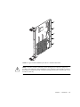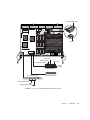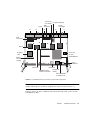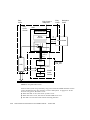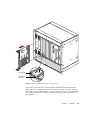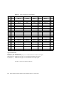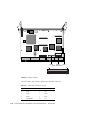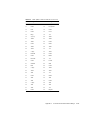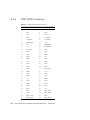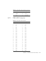
1
Netra™ CP2040 Technical
Reference and Installation Manual
Sun Microsystems, Inc.
901 San Antonio Road
Palo Alto, CA 94303-4900 U.S.A.
650-960-1300
Part No. 806-4994-10
October 2001, Revision A
Send comments about this document to: [email protected]
Copyright 2001 Sun Microsystems, Inc., 901 San Antonio Road, Palo Alto, CA 94303-4900 U.S.A. All rights reserved.
This product or document is distributed under licenses restricting its use, copying, distribution, and decompilation. No part of this product or
document may be reproduced in any form by any means without prior written authorization of Sun and its licensors, if any. Third-party
software, including font technology, is copyrighted and licensed from Sun suppliers.
Parts of the product may be derived from Berkeley BSD systems, licensed from the University of California. UNIX is a registered trademark in
the U.S. and other countries, exclusively licensed through X/Open Company, Ltd.
Sun, Sun Microsystems, the Sun logo, AnswerBook2, docs.sun.com, Java, Sun Enterprise, SunVTS, OpenWindows, Netra, Solstice DiskSuite,
OpenBoot, and Solaris are trademarks, registered trademarks, or service marks of Sun Microsystems, Inc. in the U.S. and other countries. All
SPARC trademarks are used under license and are trademarks or registered trademarks of SPARC International, Inc. in the U.S. and other
countries. Products bearing SPARC trademarks are based upon an architecture developed by Sun Microsystems, Inc. The Energy Star logo is a
registered trademark of EPA. SuperI/O is a trademark of National Semiconductor Corporation. I2C is a trademark of Phillips Semiconductor.
The OPEN LOOK and Sun™ Graphical User Interface was developed by Sun Microsystems, Inc. for its users and licensees. Sun acknowledges
the pioneering efforts of Xerox in researching and developing the concept of visual or graphical user interfaces for the computer industry. Sun
holds a non-exclusive license from Xerox to the Xerox Graphical User Interface, which license also covers Sun’s licensees who implement OPEN
LOOK GUIs and otherwise comply with Sun’s written license agreements.
Federal Acquisitions: Commercial Software—Government Users Subject to Standard License Terms and Conditions.
DOCUMENTATION IS PROVIDED “AS IS” AND ALL EXPRESS OR IMPLIED CONDITIONS, REPRESENTATIONS AND WARRANTIES,
INCLUDING ANY IMPLIED WARRANTY OF MERCHANTABILITY, FITNESS FOR A PARTICULAR PURPOSE OR NON-INFRINGEMENT,
ARE DISCLAIMED, EXCEPT TO THE EXTENT THAT SUCH DISCLAIMERS ARE HELD TO BE LEGALLY INVALID.
Copyright 2001 Sun Microsystems, Inc., 901 San Antonio Road, Palo Alto, CA 94303-4900 Etats-Unis. Tous droits réservés.
Ce produit ou document est distribué avec des licences qui en restreignent l’utilisation, la copie, la distribution, et la décompilation. Aucune
partie de ce produit ou document ne peut être reproduite sous aucune forme, par quelque moyen que ce soit, sans l’autorisation préalable et
écrite de Sun et de ses bailleurs de licence, s’il y en a. Le logiciel détenu par des tiers, et qui comprend la technologie relative aux polices de
caractères, est protégé par un copyright et licencié par des fournisseurs de Sun.
Des parties de ce produit pourront être dérivées des systèmes Berkeley BSD licenciés par l’Université de Californie. UNIX est une marque
déposée aux Etats-Unis et dans d’autres pays et licenciée exclusivement par X/Open Company, Ltd.
Sun, Sun Microsystems, le logo Sun, AnswerBook2, docs.sun.com, Java, Sun Enterprise, SunVTS, OpenWindows, Netra, Solstice DiskSuite,
OpenBoot, et Solaris sont des marques de fabrique ou des marques déposées, ou marques de service, de Sun Microsystems, Inc. aux Etats-Unis
et dans d’autres pays. Toutes les marques SPARC sont utilisées sous licence et sont des marques de fabrique ou des marques déposées de
SPARC International, Inc. aux Etats-Unis et dans d’autres pays. Les produits portant les marques SPARC sont basés sur une architecture
développée par Sun Microsystems, Inc.
L’interface d’utilisation graphique OPEN LOOK et Sun™ a été développée par Sun Microsystems, Inc. pour ses utilisateurs et licenciés. Sun
reconnaît les efforts de pionniers de Xerox pour la recherche et le développement du concept des interfaces d’utilisation visuelle ou graphique
pour l’industrie de l’informatique. Sun détient une licence non exclusive de Xerox sur l’interface d’utilisation graphique Xerox, cette licence
couvrant également les licenciés de Sun qui mettent en place l’interface d’utilisation graphique OPEN LOOK et qui en outre se conforment aux
licences écrites de Sun.
LA DOCUMENTATION EST FOURNIE “EN L’ETAT” ET TOUTES AUTRES CONDITIONS, DECLARATIONS ET GARANTIES EXPRESSES
OU TACITES SONT FORMELLEMENT EXCLUES, DANS LA MESURE AUTORISEE PAR LA LOI APPLICABLE, Y COMPRIS NOTAMMENT
TOUTE GARANTIE IMPLICITE RELATIVE A LA QUALITE MARCHANDE, A L’APTITUDE A UNE UTILISATION PARTICULIERE OU A
L’ABSENCE DE CONTREFAÇON.
Please
Recycle
Contents
Preface
xvii
Who Should Use This Book xvii
How This Book Is Organized xviii
Related References xviii
Sun Microsystems Publications xix
Reference Documents xx
Typographic Conventions xxi
Shell Prompts xxi
Accessing Sun Documentation Online xxii
Ordering Sun Documentation xxii
Sun Welcomes Your Comments xxii
1.
Introduction
1-1
1.1
Netra CP2040 System Configuration
1.2
Features of CP2040 CompactPCI Host Board
1.3
Hot-swap Support
1.4
Front Panel I/O Connectors and Indicators
1.5
Software Requirements
1.6
Determining Netra CP2040 Identification Numbers
1.6.1
1-4
1-5
1-8
1-8
1-10
Netra CP2040 Board Assembly Identification
1-10
1-10
Contents
iii
2.
1.6.2
Firmware
1.6.3
Software
Independent Hardware Vendors (IHV)
1.8
Technical Support and Warranty
Specifications
iv
1-12
1-13
2-1
Board Features and Specifications
2-1
2.1.1
CPU
2-3
2.1.2
Main Memory
2.1.3
PCI Mezzanine Module (PMC) Interface
2.1.3.1
4.
1-12
1.7
2.1
3.
1-12
2-3
2-4
Estimated Power Requirements
2.1.4
Mechanical
2.1.5
Environmental Specifications
2.1.6
Reliability/Availability
2.1.7
Compliance
2.1.8
Safety
2-5
2-5
2-6
2-6
2-7
2-8
Hardware Description
3-1
3.1
Physical
3-1
3.2
Summary Description
Functional Description
4-1
4.1
4-2
Functional Blocks
3-5
4.1.1
UltraSPARC-IIe Processor
4.1.2
Memory Address Mapping
4.1.3
SDRAM Memory
4.1.4
Firmware
4-2
4-3
4-3
4-5
4.1.4.1
System (Boot) Flash Memory
4.1.4.2
User Flash Memory
4.1.4.3
NVRAM
4.1.4.4
I 2C
Serial
4-5
4-5
EEPROM
4-5
Netra CP2040 Technical Reference and Installation Manual • October 2001
4-5
4.2
Clock Frequencies
4.3
Bus Subsystems
4.4
4.5
4.6
4-6
4.3.1
APB PCI Bus Interfaces
4.3.2
RIO_A and RIO_B Devices and E-bus Paths
4.3.3
CompactPCI Bus
4.3.4
System I/O
4.3.5
PMC and PIM Interface
4.3.6
System Management Controller
4.3.7
Watchdog Timer
4-7
4-8
4-10
CPU Reset
4.4.2
Reset Modes
4.4.3
Interrupts
4-17
Power Subsystem
4-19
4-13
4-14
4-14
4.5.1
Power Module
4.5.2
Early Power and IPMI Power
Installation
4-11
4-14
4.4.1
Hot Swap
4-7
4-9
Reset and Interrupts
4.6.1
5.
4-6
4-20
4-21
4-21
Programmable Logic Device (PLD)/Arbiter
4-22
5-1
5.1
System Configurations
5-1
5.2
Orderable Items
5.3
Pre Installation Check list
5-6
5.3.1
Board Check List
5-6
5.3.2
System Check List
5.3.3
Viewing Web Pages and Reading Documents
5.3.4
Space Requirements
5.3.5
Power Budgeting
5.3.6
Getting the Latest OBP Version
5.3.7
Complete Space, Network, and Environmental Planning
5-3
5-7
5-7
5-8
5-8
5-8
5-8
Contents
v
5.3.8
Determine Local Network IP Addresses and Hostnames
5.4
Safety
5-9
5.5
Installation Procedure Summary
5.6
Materials and Tools Required
5.7
Configuring the Netra CP2040 Hardware
5.8
5-11
5.7.1
Memory Module Installation
5.7.2
PMC Module Installation
5-11
5-12
5-13
Configuring Transition Card Hardware
5.8.1
Installing PIM Assemblies
5.8.2
Replacing the Serial EEPROM
5-14
5-14
5-14
Installing the XCP2040-TRN I/O Transition Card
5.10
Installing Netra CP2040 Card
5.11
Setting Up an Assembled Netra CP2040 Computer
5.12
Hot Swapping the Netra CP2040 Board
5-16
5-20
5-21
Line Card - Basic Hot Swap
5-21
5.12.2
Line Card - Full Hot Swap
5.12.3
Front Panel Indicators and I/O Connectors
5.12.4
Connecting Devices into a XCP2040-TRN I/O Transition Card
27
5.12.5
Adding CPCI Cards and Drivers into a Netra CP2040 Computer
5-28
5-22
To Install a CPCI Card
5.12.5.2
To Verify the Board is Seen by the System
5.12.5.3
To Obtain Additional Assistance
5.14
Software Installation
5-31
5-32
Server Configuration Guidelines
Standalone Operation
5-29
5-30
Software Installation Information
Setting Up a Network
5.15.1
5-28
Backplane and Cardcage Considerations
Initial Power-On and Firmware Update
5.14.1
5-25
5.12.5.1
5.13
5.16
5-16
5.12.1
5.12.6
vi
5-10
5.9
5.15
5-9
5-33
Netra CP2040 Technical Reference and Installation Manual • October 2001
5-32
5-29
5-29
5-28
5-
5.17
Installing Memory SDRAM Modules on the Netra CP2040 Board
5.17.1
6.
Firmware
6.1
6.2
SDRAM Memory Module Configurations
6-1
6.1.1
Firmware CORE and BPOST
6.1.2
CPOST and EPOST
6-2
6.1.3
OBP
6.1.4
Example of a show-devs Device Tree
6.1.5
An Example of devalias
6-4
6-4
Firmware NVRAM Variables
6-5
6-7
6-9
6.2.1
Firmware CORE NVRAM Variables
6-9
6.2.2
Firmware CORE Execution Control
6-9
6.2.3
OBP Configuration Variables
6.3
Firmware Memory Map
6.4
Firmware CORE Features
6.5
ASM Support
6.6
Determining Firmware Version
6.7
Field CORE/OBP Firmware Upgrade
6.8
5-33
6-1
Initialization Firmware
6.7.1
5-33
6-10
6-13
6-15
6-16
OBP Flash Update
6-18
6-19
6-20
6.7.1.1
Accessing SMC Config Block
6.7.1.2
Boot Mode Information
6.7.1.3
Using Flash Update Commands
6.7.1.4
Sequence to Boot Up the Correct OBP Image
6.7.2
SMC Firmware Update
6.7.3
IPMI Packet
6-20
6-21
6-24
6-25
6-25
6-26
Host-to-Host Communication
6-33
6.8.1
Packet
6-34
6.8.2
Event Receiver
6.8.3
Protocol
6.8.4
Generating an Event from SPARC to Send to Another SPARC
6-35
6-35
Contents
6-36
vii
6.9
SMC Implementation Note
6.10
Firmware Diagnostics
6-37
6-40
6.10.1
Setting Diagnostic Levels
6-41
6.10.2
Basic POST (BPOST)
6.10.3
Comprehensive POST (CPOST)
6.10.4
Extended POST
6.10.5
OpenBoot PROM On-Board Diagnostics
6.10.6
OpenBoot Diagnostics (OBDiag)
6-41
6-43
A. Connectors Pinouts and Switch Settings
A.1
CompactPCI Connectors
A.2
CompactPCI Backplane
6-44
6-44
A-1
A-1
A-3
A.2.1
Serial Connector- Mini Din 8 -Pin
A.2.2
RJ45 Connector
A.2.3
PMC Connectors
A.2.4
PMC J3002 Connector
A-18
A.2.5
PMC J3003 Connector
A-19
A-14
A-14
A-15
A.3
Memory Module Connector Pinout
A.4
SMC Switch Settings for HA and Non-HA Systems
A.4.1
Non-HA Systems
A.4.1.1
A.4.2
A.5
A.6
Before Installing Board in System
SCSI Termination Switch Setting
C. SunVTS™
A-24
A-25
A-26
Flash Device Selection Switches
B. Mechanical Drawings
A-24
A-24
SCSI and Flash Switch Settings
A.5.1
A-22
Before Installing Board in System
HA Systems
A.4.2.1
viii
6-42
A-26
A-27
B-1
C-1
C.1
Distribution of SunVTS Software
C-1
C.2
Installing and Starting SunVTS Software
Netra CP2040 Technical Reference and Installation Manual • October 2001
C-2
A-25
8
Index
Index-1
Contents
ix
x
Netra CP2040 Technical Reference and Installation Manual • October 2001
Figures
FIGURE 1-1
Netra CP2040 Board (without Heatsink)
FIGURE 1-2
Typical Netra CP2040 System Host or Satellite Host Board 1-3
FIGURE 1-3
Non-redundant Netra CP2040 HA configuration - One System Host Board 1-4
FIGURE 1-4
Netra CP2040 I/O Front Panel 1-9
FIGURE 1-5
Location of CP2040 Board Identification Labels
FIGURE 3-1
CP2040 Board (showing connectors) 3-2
FIGURE 3-2
CP2040 Board Layout with Key On-board Components
FIGURE 3-3
Netra CP2040 with Heatsink, SMC, Power Module and SDRAM Module 3-4
FIGURE 3-4
Solder Side of the CP2040 Board 3-5
FIGURE 3-5
CP2040 Functional Block Diagram
FIGURE 4-1
Detailed Block Diagram 4-1
FIGURE 4-2
UltraSPARC-IIe Interface 4-2
FIGURE 4-3
Memory Mapping Example
FIGURE 4-4
SDRAM Memory Interface 4-4
FIGURE 4-5
CP2040 PCI Bus Interface 4-7
FIGURE 4-6
CompactPCI Bus Interface 4-8
FIGURE 4-7
CP2040 I/O Interface
FIGURE 4-8
PCI Mezzanine Module Interface on Host Board 4-11
FIGURE 4-9
System Management Controller Interface 4-12
1-2
1-11
3-3
3-6
4-3
4-9
xi
xii
FIGURE 4-10
Simplified Reset Paths 4-16
FIGURE 4-11
Power Distribution Block Diagram
FIGURE 4-12
Selection between Early Power and IPMI Power
FIGURE 5-1
Examples of Netra CP2040 Hardware Configurations
FIGURE 5-2
Netra CP2040 Board Major Components and Connectors
FIGURE 5-3
XCP2040-TRN Transition Card
FIGURE 5-4
Single and Double-sized Memory Modules
FIGURE 5-5
Installing the PCI Mezzanine Card 5-13
FIGURE 5-6
Replacing the Serial I2C EEPROM
FIGURE 5-7
Netra CP2040 System Interface Using Two CP2040 Boards (one system controller board and
other satellite board) and Two Transition Cards 5-18
FIGURE 5-8
Netra CP2040 Installation (close-up view) 5-19
FIGURE 5-9
Releasing and Locking the Netra CP2040 Injector/Ejector Handles
FIGURE 5-10
Netra CP2040 Front Panel (front view) 5-26
FIGURE 5-11
SDRAM Memory Module Installed on a Netra CP2040 Board
FIGURE 6-1
Control Flow from Power On for Firmware CORE and Client Modules—Solaris Case
FIGURE 6-2
System Flash PROM Map 6-14
FIGURE 6-3
SW0501.switch2=0 6-21
FIGURE 6-4
SW0501.switch2=1 6-22
FIGURE 6-5
Host-to-Host Communication 6-33
FIGURE 6-6
Basic POST Services 6-41
FIGURE 6-7
POST Enables OEMs to add Diagnostics
FIGURE A-1
CP2040 Board Connectors
FIGURE A-2
J1 Connector A-3
FIGURE A-3
CP2040 Board J2 Connector
A-5
FIGURE A-4
CP2040 Board J3 Connector
A-7
FIGURE A-5
CP2040 J4/P4 Connector A-9
FIGURE A-6
CP2040 Board J5/P5 Connector
FIGURE A-7
CP2040 Front Panel TTYA Diagram A-14
4-19
4-21
5-2
5-5
5-6
5-12
5-15
6-43
A-2
A-11
Netra CP2040 Technical Reference and Installation Manual • October 2001
5-24
5-34
6-2
FIGURE A-8
RJ45 Ethernet Connector Diagram A-14
FIGURE A-9
J3001 Connector
FIGURE A-10
Memory Module Connectors J0601 and J0602 A-21
FIGURE A-11
Setting Switches to Closed Position A-24
FIGURE A-12
SW0501 Position for non-HA Systems A-25
FIGURE A-13
Location of SW0501 on SMC Module
FIGURE A-14
SW0501 Switch Setting for HA Systems
FIGURE A-15
Switch Setting Legend
FIGURE A-16
SCSI Termination Switch Setting Example
FIGURE A-17
SCSI Switch Selections and SMC on the CP2040
FIGURE B-1
Mechanical Drawing of the CP2040 Front Panel B-2
FIGURE B-2
Mechanical Dimensions of the CP2040 B-3
FIGURE B-3
Mechanical Dimensions of the Heatsink and Memory Module B-4
A-16
A-25
A-26
A-26
A-28
A-29
Figures
xiii
xiv
Netra CP2040 Technical Reference and Installation Manual • October 2001
Tables
TABLE 1-1
Feature Summary
TABLE 2-1
Netra CP2040 Physical Dimensions 2-1
TABLE 2-2
Specifications Summary 2-1
TABLE 2-3
System Compatibility Attributes 2-2
TABLE 2-4
CompactPCI Bus Interface 2-2
TABLE 2-5
CPU Specification 2-3
TABLE 2-6
Memory Specification 2-3
TABLE 2-7
Netra CP2040 Memory Module Configurations 2-4
TABLE 2-8
PMC Interface Specification 2-5
TABLE 2-9
Estimated Power Dissipation for the Netra CP2040 Board 2-5
TABLE 2-10
Environmental Conditions and Limits 2-6
TABLE 2-11
Reliability Prediction for Board Level MTBF
TABLE 4-1
Clock Frequencies
TABLE 4-2
Host-SMC Commands
TABLE 4-3
Publicly Available Reset Operating Modes 4-15
TABLE 4-4
UltraSPARC Hardware Interrupts (as inputs to IChip2) 4-17
TABLE 5-1
SPARCengine Netra CP2040 Hardware Configurations 5-3
TABLE 5-2
Preinstallation Checklist
TABLE 5-3
Netra CP2040 IO Configurations 5-11
1-5
2-6
4-6
4-13
5-8
xv
xvi
TABLE 5-4
Installation Information Work Sheet
TABLE 6-1
Firmware CORE and BPOST Flow of Execution 6-3
TABLE 6-2
Key Sequences
TABLE 6-3
NVRAM Configuration Variables
5-31
6-9
6-10
TABLE 6-4
OBP Environment Variable Settings for Executing the POST Modules 6-12
TABLE 6-5
Monitor Commands CORE 6-15
TABLE 6-6
Chassis Configuration Example 6-30
TABLE 6-7
IPMI Packet
TABLE 6-8
OBDiag -- Diagnostics Test printout 6-44
TABLE A-1
J1/P1 Connector Pin Assignments
A-3
TABLE A-2
J2/P2 Connector Pin Assignments
A-6
TABLE A-3
J3/P3 Connector Pin Assignments
A-8
TABLE A-4
J4/P4 Connector Pin Assignments
A-9
TABLE A-5
J5/P5 Connector Pin Assignments
A-12
TABLE A-6
Serial Mini Din 8-pin Connector Pinouts
TABLE A-7
CP2040 Front Panel Ethernet Connector Pinout
TABLE A-8
PMC J3001 Connector Pinouts A-16
TABLE A-9
PMC J3002 Connector Pinouts A-18
TABLE A-10
PMC J3003 Connector Pinouts A-19
TABLE A-11
Memory Module Connector 1 Pinout (Bottom Side) A-22
TABLE A-12
Memory Module Connector 2 Pinout (Bottom Side) A-23
TABLE A-13
Flash Device Switch Setting (S1W801)
TABLE A-14
SCSI Termination Switch Setting (SW2401)
6-30
A-14
A-15
A-27
A-28
Netra CP2040 Technical Reference and Installation Manual • October 2001
Preface
The Netra™ CP2040 CompactPCI board is designed to address critical applications
in the core network and access network infrastructures, including wireless
infrastructure and access networks.
The Netra CP2040 CompactPCI board incorporates a 500-MHz UltraSPARC™ IIe
processor and runs on Solaris™ 8 Operating Environment. This board also supports
advanced architectural capabilities for next-generation network infrastructure
requirements.
The Netra™ CP2040 Technical Reference and Installation Manual (P/N 806-4994-xx)
describes the functions of the CP2040 board, its controls, indicators, connectors,
pinouts, boot sequence, and specifications. It also provides some mechanical
drawings of the board.
Who Should Use This Book
The Netra™ CP2040 Technical Reference and Installation Manual is written for computer
hardware engineers, system programmers, computer technicians, and others
involved in the integration of the Netra CP2040 board. References are provided for
further details.
xvii
How This Book Is Organized
The Netra™ CP2040 Technical Reference and Installation Manual is organized as
follows:
Chapter 1 “Introduction” explains the capabilities and major features of the
Netra CP2040 board.
Chapter 2 “Specifications” provides a summary of specifications of the
Netra CP2040.
Chapter 3 “Hardware Description” provides a short description of the function of
each block on the Netra CP2040.
Chapter 4 “Functional Description” describes the sequence of events that occur at
power up in a reference configuration.
Chapter 5 “Installation” describes how to install the Netra CP2040 board in
different configurations.
Chapter 6 “Firmware” describes the structure and function of initialization
firmware. It also provides information on the Netra CP2040 system OpenBoot
firmware.
Appendix A “Connectors Pinouts and Switch Settings” describes the pinouts of the
connectors on the Netra CP2040. Also provided are the illustrations of all the major
connectors.
Appendix B “Mechanical Drawings” contains some mechanical drawings of the
Netra CP2040 board.
Appendix C “SunVTS™, describes the Sun Validation Test Suite (SunVTSTM) which
is a comprehensive software package that tests and validates the CP2040 by
verifying configuration and functions of most hardware controllers and devices on
the motherboard.
Related References
Specifications and Standards
■
xviii
IEEE Standard 1275-1994, Standard For Boot (Initialization, Configuration) Firmware,
Core Practices and Requirements
Netra CP2040 Technical Reference and Installation Manual • October 2001
■
■
■
IEEE Standard 1275.1-1994, Standard For Boot (Initialization, Configuration) Firmware,
ISA Supplement for IEEE P1754 (SPARC)
IEEE Standard P1275.6/D4, Standard For Boot (Initialization, Configuration) Firmware,
64 Bit Extensions
PCI Bus Binding to IEEE 1275-1994, Standard for Boot (Initialization, Configuration)
Firmware, Revision 1.0, 14 April 1994, Prepared by the Open Firmware Task Force
of the PCI Alliance
Integrated Circuit Specifications:
SME1040 Highly Integrated 64-bit RISC Processor, PCI Interface Data Sheet
(805-0086-02)
■ STP2003QFP PCI Input Output Controller (PCIO) User’s Manual
(802-7837-01)
■ STP2210QFP Reset/Interrupt/Clock Controller (RIC) User’s Manual
(805-0167-01)
■ SME2411BGA-66 Advanced PCI Bridge (APB) User’s Manual
(805-1251-01)
■ Intelligent Chassis Management Bus Bridge Specification, version 1.0, published by
Intel, Hewlett-Packard, NEC and Dell
Sun Microsystems Publications
For all Sun published material you may go to the following URL:
http://docs.sun.com/
System Architecture:
■
■
■
■
■
■
■
■
■
■
■
The SPARC Architecture Manual, Version 9, David L. Weaver and Tom Germond,
editors, PTR Prentice Hall (ISBN: 0130992275)
PCI System Architecture, by Shanley and Anderson, Inc. MindShare Press
(ISBN: 0201309742)
Solaris 8 7/01 Release Notes (SPARC Platform Edition) (806-7942-11) FCS
Solaris 8 Installation Supplement (806-7500-10)
Solaris 8 Desktop User Supplement (806-7501-10)
Solaris 8 System Administration Supplement (806-7502-10)
Solaris 8 Software Developer Supplement (806-7503-10)
Open Boot 3.X Command Reference Manual (802-5837-10)
Open Boot 3.X Command Supplement for PCI (Solaris 2.5.1, 8/97) (805-1627-10)
Writing Fcode 3.x Programs (802-6287-10)
ASM Utilization and Calibration Application Note (805-4877-01)
Preface
xix
■
SunVTS™ 2.1 SunVTS User’s Guide (Part No. 802-7299) August 1997, Rev. A
■
SunVTS™ Quick Reference Card (Part No. 802-7301) August 1997, Rev. A
■
SunVTS™ 2.1.3 Test Reference Manual (Part No. 805-4163-10) May 1998, Rev. A
SunVTS 4.2 User’s Guide (P/N 806-6515-xx)
SunVTS 4.2 Test Reference (P/N 806-6516-xx)
■
■
Reference Documents
■
■
■
■
■
■
■
■
■
■
■
XCP2040-TRN I/O Transition Card Manual for Netra™ CP2040 CPCI Board (Part
No. 806-6743-xx)
Read Me First Netra™ CP2040 (P/N 816-0610-xx)
PICMG® 2.0 R3.0 CompactPCI® Specification
PCI Local Bus Specification, Revision 2.1, PCI Special Interest Group, Portland
PCI System Architecture, by Shanley and Anderson, MindShare Press
OpenBoot 3.x Command Reference, Sun Microsystems (Part No.802-5837-10, Rev A)
PCI Bus Binding to IEEE 1275-1994, Standard for Boot (Initialization, Configuration)
Firmware, Revision 1.0, 14 April 1994, Prepared by the Open Firmware Task Force
of the PCI Alliance
OpenBoot 3.x Command Supplement for PCI, Sun Microsystems (805-1627-10)
The SPARC Architecture Manual, Version 9, David L. Weaver and Tom Germond,
editors, PTR Prentice Hall
SPARCengine™ CP1400/CP1500 Programmer Reference Guide for Solaris
(Part No. 806-0180-xx)
PCIO PCI Input Output Controller User’s Manual (802-7837-xx)
To view Sun technical manuals on-line, visit our internet site at
http://www.sun.com/microelectronics/manuals/index.html
xx
Netra CP2040 Technical Reference and Installation Manual • October 2001
Typographic Conventions
Typeface
Meaning
Examples
AaBbCc123
The names of commands, files,
and directories; on-screen
computer output
Edit your .login file.
Use ls -a to list all files.
% You have mail.
AaBbCc123
What you type, when
contrasted with on-screen
computer output
% su
Password:
AaBbCc123
Book titles, new words or
terms, words to be emphasized
AaBbCc123
Command-line variable;
replace with a real name or
value
Read Chapter 6 in the User’s Guide.
These are called class options.
You must be superuser to do this.
To delete a file, type rm filename.
Shell Prompts
Shell
Prompt
C shell prompt (in Solaris)
machine_name%
C shell superuser prompt (in Solaris)
machine_name#
Bourne shell and Korn shell prompt
$
Bourne shell and Korn shell superuser prompt
#
OBP prompt
ok
Preface
xxi
Accessing Sun Documentation Online
The docs.sun.comsm web site enables you to access Sun technical documentation
on the Web. You can browse the docs.sun.com archive or search for a specific book
title or subject at:
http://docs.sun.com
Ordering Sun Documentation
Fatbrain.com, an Internet professional bookstore, stocks select product
documentation from Sun Microsystems, Inc.
For a list of documents and how to order them, visit the Sun Documentation Center
on Fatbrain.com at:
http://www1.fatbrain.com/documentation/sun
Sun Welcomes Your Comments
We are interested in improving our documentation and welcome your comments
and suggestions. You can email your comments to us at:
[email protected]
Please include the part number of your document in the subject line of your email.
xxii
Netra CP2040 Technical Reference and Installation Manual • October 2001
CHAPTER
1
Introduction
The Netra™ CP2040 CompactPCI board incorporates a 500-MHz UltraSPARC™ IIe
processor and uses the Solaris™ 8 Operating Environment in order to meet
enhanced availability requirements. This board also supports advanced architectural
capabilities for next-generation network infrastructure requirements.
The Netra CP2040 CompactPCI board is a crucial building block in developing
carrier-grade systems. It can function as a system controller or a satellite board. As a
modular solution, the Netra CP2040 is easy to configure and install. It is designed to
support next-generation requirements, in conjunction with the Netra CP2060/
CP2080 satellite CompactPCI boards, for continuous uptime in the core network and
access network infrastructures.
The Netra CP2040 board is in compliance with PICMG CompactPCI 3.0. In the
System Host role, the Netra CP2040 Host board can support Basic, Full and High
Availability hot swap.
FIGURE 1-1 shows the Netra CP2040 board.
1-1
RIO A
J5
J4
Advanced
2
PCI bridge I C (MAC address)
21554
SMC
PCI bridge
Connector
J3
J2
J1
3
2
SV2
8F 1
2
1
SW1801
RIO B
SW2401
4
SV4
9J
PMC
connectors
Clock chip
for CPU
SuperI/O
chip
UltraSPARC IIe
Debug
connector
(J3101)
TTY A
COM port
Dual SCSI
Ethernet A
SDRAM memory
module connectors
NVRAM &
battery
Serial EEPROM
for Arbiter PLD
FIGURE 1-1
1-2
Netra CP2040 Board (without Heatsink)
Netra CP2040 Technical Reference and Installation Manual • October 2001
J5
J4
P
J3
M
C
J2
AB
OR
T
RE
SE
T
ALA
RM
/US
ER
RE
AD
Y
J1
ETH
ER
NE
T
CP
201
0/5
00
CO
M
HO
TSW
AP
FIGURE 1-2
!
Typical Netra CP2040 System Host or Satellite Host Board
Note – The CPU module, heatsink, System Management Controller, and power
module are all integral to the CP2040 board. Any attempt to disassemble or replace
these devices on the board will void the warranty (see FIGURE 3-2 and FIGURE 3-3 for
location of devices).
Chapter 1
Introduction
1-3
1.1
Netra CP2040 System Configuration
Systems that conform to CompactPCI specifications require differentiation of chassis
board slots depending upon the mode in which a board is to function.
To function as a System Host, a CP2040 processor board has connections that include
those that distribute PCI clocks and receive interrupts from peripherals. It must also
be situated in a System Host slot in the CompactPCI segment because only these
chassis slots have backplane wiring with the full set of connections required to
enable the System Host function. The CP2040 boards can control CompactPCI
peripheral hardware on their own account. They assume a System Host role if they
are installed into a PICMG system slot because a special signal is enabled in this slot.
A system slot is marked with an open triangle legend specified in CompactPCI
Specification, PICMG 2.0 R3.0.
The CP2040 board can be installed in one of the remaining (non-System Host) slots if
the user wants to use it as a Satellite Host.
The simplest configurations of the Netra CP2040 is shown in FIGURE 1-3. They contain
one System Host that may supply any input/output (I/O) required by itself (a), or
use an added I/O board (b). There is no redundancy in either of these arrangements.
I/O
I/O
System
Host
System
Host
I/O
I/O
CompactPCI Bus
CompactPCI Bus
(a) System host board
(b) I/O board added
FIGURE 1-3
Non-redundant Netra CP2040 HA configuration - One System Host Board
Satellite Hosts do not control any peripheral I/O outside their own board and are
typically used to perform independent processor-intensive tasks.
1-4
Netra CP2040 Technical Reference and Installation Manual • October 2001
1.2
Features of CP2040 CompactPCI Host
Board
The CP2040 is designed to support hot-swap operation, System Management, and
environmental monitoring. These functions are implemented in the System
Management Controller which is designed as a mezzanine module on the CP2040
board. In addition, the CP2040 has PCI Mezzanine Connectors that enable
connection of compatible PMC peripherals. The CP2040 supports two 10/100Mbps
ethernet ports and two serial ports, two universal serial bus (USB) ports, two SCSI
ports, floppy port, parallel port and PS/2 keyboard and mouse port.
A summary of key features of the CP2040 board is given in TABLE 1-1.
TABLE 1-1
Feature Summary
Feature
CPU
Memory
Description
■
UltraSPARC IIe 500 MHz processor with internal 256KB
integrated cache
No onboard memory. Up to 2GB memory is supported via the
following memory modules:
■
■
■
256MB, 512MB, 1GB
The 1GB memory module is double the size of other memory
modules. Installation of this memory module will make the
PMC slot unusable
A maximum of two memory modules can be stacked
together.
cPCI Bus interface
■
64 bit, 33 MHz,5V bus interface
Power requirement
■
Typical at 20W (typical with 256MB) and 32W (maximum
with 2GB) at 500MHz (excluding PMC power)
PICMG compliance
■
Meets PICMG CompactPCI 3.0 and PCI revision 2.1
specifications
Availability
■
Carrier-grade
Host-mode support
■
Universal
Chapter 1
Introduction
1-5
TABLE 1-1
Feature Summary (Continued)
Feature
Description
The onboard SMC supports the following IPMI commands as
specified in the IPMI Specification v1.1.0 Rev 1.1:
■
Global commands
■
Watchdog Timer commands. Level 1 and Level 2 Watchdog
Timer commands are supported.
■
Event commands
■
FRU commands
■
Sensor Device commands
PICMG compliance
■
PICMG CompactPCI 3.0 and PCI standards
hot-swap support
■
Basic, Full and HA hot swap supported when installed in the
System Controller slot or Alternate System Controller slot of
a Sun proprietary HA hot-swap backplane.
Supports both basic and full hot-swap functions when
installed in the System Controller slot of a standard full hotswap chassis.
IPMI compliance
■
Operating system
■
Solaris 8 1/01 or subsequent compatible version with CD 3.1
Ethernet support
■
Dual 10/100Mbit Ethernet with MII interface to the
backplane. Ethernet A port is also routed to the front panel
with onboard PHY and magnetics (only front or rear access
of this Ethernet A port is allowed, no simultaneous accesses
to this port are permitted)
I/Os
■
Dual Async serial ports via dual mini-DB9 (non-standard)
connectors on transition card
■
One console serial port brought to front panel via a DIN 8
connector
■
Dual USB ports on the transition card. Each USB port is
driven by individual controllers (both USBs routed to the
cPCI backplane via the J5/P5 connector)
■
IPMI I2C bus is routed to the cPCI backplane via J1/P1. This
can be bused to all slots on the cPCI backplane
■
One I2C buss routed to the transition board via the J5/P5
connector
■
Two RS 232 serial ports
Two SCSI ports
One cutout to support the use of a PIM card on the transition
card panel.
Access to a floppy port, parallel port, a keyboard and a
mouse port. The use of these ports would consume 2U space.
Provision to add one IHV-supplied PCI Interface Module
(PIM) I/O port when used with transition card
Backplane I/O—
accessible through rear
transition card faceplate
■
■
■
■
1-6
Netra CP2040 Technical Reference and Installation Manual • October 2001
TABLE 1-1
Feature Summary (Continued)
Feature
cPCI interface
Description
■
Compliant with PICMG 2.0 R3.0 Compact PCI Bus
Specification for 33 MHz PCI speed
■
Supports both 32-bit and 64-bit Compact PCI I/O boards
■
cPCI interface supports only +5Volt PCI environment
■
Compliant with PICMG 2.1 R1.0 Compact PCI hot swap
■
Specification in Basic, Full and HA hot swap
■
Compliant either as a System Controller or as a satellite
board
Disk interface
■
Dual single ended channel Ultra-SCSI that can support up to
40MB/sec data transfer rate. Both SCSI connectors are
brought out to the Transition Card.
PMC Support
■
Supports one PMC slot
Compliant with CMC Standard IEEE-P1386.1, PMC
mezzanine modules specification
PMC slot supports only +5V PCI environment
Mapping of 64 user-defined PMC I/O signals to J3/P3 on
cPCI backplane
Provision for adding one IHV supplied PMC expansion port
on front panel
■
■
■
■
PIM support
Watchdog timer
■
Compliant with PMC I/O Module Standard, VIT 36-199X,
Draft VTA Standards Organization can be achieved when
using Sun designed Transition board for CP2040.
Two levels of watchdog timer are supported:
■
■
Level 1 causes an interrupt to the SPARC processor.
Level 2 causes the system to reset, power down, or power
cycle.
NVRAM/TOD
8KB of non-volatile memory storage and TOD with battery
System flash
1 MB onboard
User flash
■
8MB (2 x 4MB)
Building compliance
NEBS Level 3
Flash update
Supported from downloaded file
Physical dimensions
Standard 6U cPCI form factor. Fits into a single cPCI slot with two
memory modules installed.
Chapter 1
Introduction
1-7
1.3
Hot-swap Support
The Netra CP2040 is capable of performing basic hot swap, full hot swap and HA
(high availability) hot swap of a Sun-supported cPCI I/O card:
1. Hot insertion of any Hotswappable boards.
2. Basic hot swap: This feature provides hardware features required to perform hot
swap, but operator intervention is required to execute software steps such as
system configuration and installation of device drivers.
3. Full hot swap: This feature provides both hardware and software features
required for software connection protocol. Board software connection control
resources provide the following:
■
■
■
ENUM# signal to indicate service requests to the system host, which include
adding or removing software drivers for boards that have been inserted or
extracted.
Hot-swap switch: to indicate an operator wishes to extract a board.
LED: which is illuminated to indicate that it is safe to extract a board without
interrupting system operation.
4. HA hot swap: In a high availability (HA) system, hardware and software is added
to allow a higher degree of system control. The following signals are used to
control each slot in the system:
■
■
■
1.4
BD_SEL#: The shortest pin on a system backplane - this pin is the last to mate
and first to break contact. This ensures that sensing takes place at a time when
all other pins are reliably connected.
HEALTHY#: A radial signal that signals a board is suitable to be released from
reset and allowed onto the PCI bus.
PCI-RST#: Driven by the system host, platforms can use this signal to control
the electrical connection process - boards cannot come out of reset until
HEALTHY# signal is indicated.
Front Panel I/O Connectors and
Indicators
FIGURE 1-4 illustrates the indicators and I/O connectors on the CP2040 board front
panel. The front panel connectors, buttons and LEDs are described below.
■
■
1-8
One peripheral mezzanine card (PMC) I/O bezel
ABORT: An abort push button switch; passes an XIR signal to the SMC
Netra CP2040 Technical Reference and Installation Manual • October 2001
■
■
■
■
■
■
■
RESET: A reset push button switch; passes an Button Power-on-Reset (BOR)
signal to the SMC
ALARM/USER: A red/green (two color) LED— for board status,
READY: A green power LED, sourced from the power module
Ethernet RJ45 Ethernet connector (10/100 Mbps)
COM 8-pin DIN RS-232 serial I/O port
A blue LED for hot-swap status, sourced from the SMC
A hot-swap latch that has to be closed at insertion of board and opened prior to
extraction of the CP2040.
P
M
C
ABORT
RESET
ALARM/USER
READY
ETHERNET
microsystems
CP2040-500
COM
HOTSWAP
FIGURE 1-4
Netra CP2040 I/O Front Panel
Chapter 1
Introduction
1-9
Note – CP2040-500 on the front panel indicates a CP2040 board with 500 MHz CPU.
1.5
Software Requirements
These CP2040 board requires Solaris TM 8 1/01 Operating Environment and
compatible versions. A CP2000 supplemental CD is available that offers additional
features on the CP2040 board such as driver support and satellite hot-swap support.
For further information on how to obtain the CD 3.1, please contact your Field
Application Engineer.
1.6
Determining Netra CP2040
Identification Numbers
1.6.1
Netra CP2040 Board Assembly Identification
The Netra CP2040 board date code, part number, serial number and revision number
can be found on stickers located on the board (see FIGURE 1-5). The board part
number (for example, 5015721) is the first seven digits on the barcode label. The next
six digits is the serial number (for example, 000230).
1-10
Netra CP2040 Technical Reference and Installation Manual • October 2001
MAC address label
XX
SV2
8F
XX
1
2
XX
2
1
SW1801
SV2
8F 1
2
3
4
SV4
9J
xxxxxx
SW2401
U3207
Revision #
Product dash
Product part number
Date code
5721-04 REV 09
08/2001
ASSEMBLED IN CANADA
Country
of origin
Subcon label
XXXXXXXXXXX
Sun barcode label
CM barcode label
5015721000230
Board part number
Board serial number
FIGURE 1-5
Location of CP2040 Board Identification Labels
Chapter 1
Introduction
1-11
1.6.2
Firmware
This section shows how to display the OBP version, SMC firmware, PLD and SMC
FPGA information. To view the banner containing this information, perform the
following:
■
For example, if running OBP, at the OK prompt type:
ok .version
SMC Firmware Release 3.2.14 Platform ID 10
FPGA Version 0.9
PLD Version 0.5
Firmware CORE Release 0.0.16 created 2001/6/8 16:43
Release 4.0 Version 20 created 2001/06/09 11:54
cPOST version 1.0.2 created 2001/5/14
ok
1.6.3
Software
To determine the release number of Solaris Operating Environment, at the
machine_name prompt type:
machine_name uname -r
The machine will display the OS version in the following format:
For example, X.X.X or X.X
1.7
Independent Hardware Vendors (IHV)
Independent hardware vendors generally supply non-Sun parts, components, and
peripherals such as the PMC cards, enclosures, hard disk drives, floppy disk drives,
CD-ROM drives, monitors, keyboards, mouse devices.
A list of these IHVs is available on the internet at the URL at the general availability
of this product:
http://www.sun.com/microelectronics/boards/cp/2040/ihvprod.html
1-12
Netra CP2040 Technical Reference and Installation Manual • October 2001
This web site will be updated periodically as additional items are tested for
compatibility with the Netra CP2040 board.
Please contact your Field Application Engineer for more information.
An enclosure is required to set up a CP2040 system, but is not supplied by Sun
Microsystems Inc.
1.8
Technical Support and Warranty
The following information is applicable only at the GA (General Availability) of the
product.
Should you have any technical questions or issues that are not addressed in the
Netra™ CP2040 Technical Reference and Installation Manual or on the web site, contact
your local sales representative. To contact Sun Enterprise Services in the U.S.,
phone (800) USA-4SUN (800-872-4786). To find the Sun Enterprise Services
Worldwide Solution Center nearest you go to this URL:
http://www.sun.com/service/contacting/solution.html
When you call Sun Enterprise Services, be sure to identify the product by the
product name: Netra CP2040. Please also provide its part number (see Section 1.6
“Determining Netra CP2040 Identification Numbers” on page 1-10).
The CP2040 comes with a warranty. Should your board fail during the warranty
period, contact your local Sun Enterprise Services representative for instructions.
Before you call, get the motherboard date code, part number and serial number from
the stickers as described in Section 1.6 “Determining Netra CP2040 Identification
Numbers” on page 1-10.
Chapter 1
Introduction
1-13
1-14
Netra CP2040 Technical Reference and Installation Manual • October 2001
CHAPTER
2
Specifications
This chapter provides the Netra CP2040 board specifications.
2.1
Board Features and Specifications
The physical dimensions of the CPU board are given in TABLE 2-1.
TABLE 2-1
Netra CP2040 Physical Dimensions
CPU Board Parameter
6U CompactPCI Form Factor
Height
9.2” in. (233.68 mm)
Length
6.2 in. (157.48 mm.)
Depth
0.8 in. (20.32 mm.)
A summary of key features of the CP2040 board is given in TABLE 2-2.
TABLE 2-2
Specifications Summary
Property
Netra CP2040
CPU
500 MHz UltraSparc-IIe
Cache
Integrated, 256KB, internal L2 cache operating in 2:2 mode
Memory—SDRAM
256MB to 2GB (maximum) SDRAM memory in stackable modules
Memory—boot flash
1MB Boot Flash (firmware) on board
Memory—user flash
8MB on board
CompactPCI specification
compliance
PICMG 2.0 R3.0 Bus; 64bit, 33MHz, 5V bus interface
PICMG 2.1 R1.0 hot swap
PICMG 2.9 D0.6 System Management
2-1
TABLE 2-2
Specifications Summary (Continued)
Property
Netra CP2040
Host modes support within
system
System Host mode, Satellite Host mode
System management
Control by a modular System Management Controller
NVRAM
8KB with replaceable battery
Firmware support
IPMI Protocol with System Management Controller (SMC);
Local Advanced System Monitoring (ASM);
Host CPU (UltraSPARC-IIe) communication;
Flash update execution from firmware;
CompactPCI HA/hot swap support
Operating System
Solaris 8 1/01
RTOS support
VxWorks and Chorus at GA (General Availability)
Front Panel controls/
indicators
Reset (POR) and Interrupt (XIR) push buttons;
Blue LED, Alarm LED, Power LED;
1PMC front-panel I/O cut-outs
Hot swap Latch
PMC card support
1 PMC card
Transition Card
Connects I/O on J3 for (PMC/PIM) to rear panel; and J4/J5 includes Ethernet, serial,
and USB channels
The system compatibility attributes are given in TABLE 2-3.
TABLE 2-3
System Compatibility Attributes
Parameter
Description
System Host Capability
Yes
Satellite Host Capability
Yes
CompactPCI Compliance
64bit, 33MHz, 5V bus interface; PICMG 2.0
R3.0 Bus specification
PICMG 2.1 R1.0 hot swap specification
PICMG 2.9 D0.6 System Management
specification
NEBS Compliance
NEBS level 3 compliance
A detailed description of compactPCI bus interface is given in TABLE 2-4.
TABLE 2-4
2-2
CompactPCI Bus Interface
Parameter
Description
Configuration
6U +5V, 33 MHz, 64 bits with support for seven additional
external bus slots.
Connector
2mm pin-and-socket (IEC-1076-4-101)
Netra CP2040 Technical Reference and Installation Manual • October 2001
2.1.1
CPU
The CPU specification is given in TABLE 2-5.
TABLE 2-5
2.1.2
CPU Specification
Property
Netra CP2040
CPU
500 MHz UltraSparc-IIe - 370-pin ceramic PGA package soldered to
board
Architecture
Sun 4U; SPARC V9 architecture with the VIS Instruction Set
Cache
Integrated, 256KB, 4-way, set-associative internal L2 cache
PCI bus local interface
PCI Bus 2.1 compatible, 33/66 MHz, 32-bit, 3.3V (internal to board
only, does not come on connector)
Main Memory
The memory specification is given in TABLE 2-6.
TABLE 2-6
Memory Specification
Property
Netra CP2040
Memory size—min
256MB
Memory size—max.
2GB
Memory configuration -- soldered
no soldered memory
Memory configuration -- stackable
one or two custom stackable modules; see TABLE 2-7 for
allowable combinations
Memory type
3.3V, DRAM with ECC
LVTTL-compatible CMOS; configured on bus width of
64-bit + 8-ECC bits
Interface
unbuffered
Chapter 2
Specifications
2-3
The Netra CP2040 memory module configurations are given in TABLE 2-7.
TABLE 2-7
Netra CP2040 Memory Module Configurations
Bottom SDRAM Module
PN and Specification
Top SDRAM Module
PN and Specification
Total Memory
Available on Board
375-3024-xx
256MB
none
256MB
375-3024-xx
256MB
375-3024xx
256MB
512MB
375-3025-xx
512MB
none
512MB
375-3025-xx
512MB
375-3024-xx
256MB
768MB
375-3024-xx
256MB
375-3025-xx
512MB
768MB
375-3025-xx
512MB
375-3025-xx
512MB
1024MB
375-3026-xx
1024MB
none
1024MB
375-3026-xx
1024MB
375-3024-xx
256MB
1280MB
375-3026-xx
1024MB
375-3025-xx
512MB
1536MB
375-3024-xx
256MB
375-3026-xx
1024MB
not supported
375-3025-xx
512MB
375-3026-xx
1024MB
not supported
375-3026-xx
1024MB
375-3026-xx
1024MB
2048MB
Note – Any two modules in any supported memory configuration can be installed
in any combination (256MB, 512MB, or 1GB). However, if two memory modules
need to be installed and one of the modules is double-sized, it should be installed on
the bottom.
2.1.3
PCI Mezzanine Module (PMC) Interface
The PMC interface specification is given in TABLE 2-8.
2-4
Netra CP2040 Technical Reference and Installation Manual • October 2001
TABLE 2-8
PMC Interface Specification
Property
Netra CP2040
PMC module interfaces on system board
one: PMC
Interface IEEE P1386.1 compliance
with draft 2.1
Connector configuration, PMC (P1386 designations)
J11, J12 carry PCI signals; J14 module
I/O is connected to cPCI backplane J3;
J13 connector is not fitted
PMC connections to cPCI backplane
PMC I/O on J3
PCI clock
33MHz
PCI bus width
32-bit
Netra CP2040 keyed for signalling voltage
5V
Max power load—per module, combined 5V and 3.3V
rails
7.5 W1
1. sum power allowable from any one rail or both rails together.
2.1.3.1
Estimated Power Requirements
The estimated power dissipation for Netra CP2040 Board is given in TABLE 2-9.
TABLE 2-9
2.1.4
Estimated Power Dissipation for the Netra CP2040 Board
Configuration (Netra
CP2040 with 500MHz)
Watts Dissipation (Typical)
256 MBytes memory
Low power ~20 Watt typ. PCI mezzanine card and transition card
not included
(~32 Watt maximum)
Input power
+5V/3.3V/12V/-12V from CPCI backplane (with PCI mezzanine
card support)
Mechanical
These products comply with the mechanical specifications to be found in the
CompactPCI specification PICMG 2.0 R3.0.
Chapter 2
Specifications
2-5
2.1.5
Environmental Specifications
The environmental conditions and limits are given in Table 2-10.
Table 2-10
Environmental Conditions and Limits
Limits1
Ambient Conditions
Transportation and storage
temperature
-400 C for 72 hrs. max.
+700 C for 72 hrs. max.
Transportation and storage
humidity
5% relative humidity,
non-condensing
95% relative humidity
non-condensing
Operating temperature
0 degrees C (-5 degrees C short
term)
40 degrees C (55 degrees C
short term)
Operating humidity
5% relative humidity,
non-condensing
85% RH (90% relative humidity
short term) non-condensing
Shock and vibration
As stated in NEBS GR-63 CORE specifications, section 4.3.1 and
4.3.2 for shock criteria and 4.4.3 for vibration criteria;
MIL-STD 810E, Method 514.4, CAT I
MIL-STD 810E, Method 516.4, II-3.2
Electrostatic discharge
GR-1089 Section 2
Altitude
0 foot to 10,000 feet operational (0 meter to 3408 meters)
Cooling
300 linear feet per minute (LFM) (minimum requirement)
1. Short term, in this column, refers to a period of not more than 96 consecutive hours and a total of not more than
15 days in 1 year.
2.1.6
Reliability/Availability
Reliability prediction is the first measurement point of expected behavior of the
inherent design mean time between failures (MTBF), of the product. MTBF values
calculated are shown in Table 2-11.
.The reliability prediction for board level MTBF is given in Table 2-11.
Table 2-11
2-6
Reliability Prediction for Board Level MTBF
Items
MTBF (hours)
Annualized Failure
Rate (AFR in%)2
CP2040 board1 + 0MB memory
200,800
4.00
CP2040 board + 1x512 MB memory
159,600
5.34
CP2040 board + 2x256 MB memory
135,300
6.27
Netra CP2040 Technical Reference and Installation Manual • October 2001
Table 2-11
Reliability Prediction for Board Level MTBF (Continued)
Items
MTBF (hours)
Annualized Failure
Rate (AFR in%)2
CP2040 board + 1x1GB memory
158,780
5.37
CP2040 board + 2x1GB memory
131,300
6.45
XCP 2040-TRN card
823,050
1.06
0
1. Board ambient temperature at 40 C
2. AFR (%) is Annualized Failure Rate based on 8,760 power on hours (POH) per year.
2.1.7
Compliance
All printed wiring boards (PWBs) are manufactured by UL recognized
manufacturers, with a flammability rating of 94-V1 or better. Compliance with EMI
and safety regulations for products including the Netra CP2040 is entirely the
responsibility of OEMs. The CP2040 has passed FCC Class B tests in representative
enclosures.
The CP2040 boards are intended to be incorporated into systems meeting the
following regulations/compliances:
■
■
■
■
■
■
■
■
■
USA FCC part 15 Class B
USA Safety UL 1950
Canadian ICES Class B
Canadian Safety CSA C22.2 Number 950
European Union EMC CE Mark EN55022 & EN50082-1
European Union Safety CE Mark EN 60950
European Union Safety TÜV
Japanese EMC VCCI Class B
NEBS Level 3
Board requirements for NEBS Level 3 criteria that provide the highest assurance
of product operability with minimal service interruptions over the life of the
equipment. It includes the following categories and all associated sections and
subcategories:
■
■
NEBS GR-63-CORE, Issue 1, October 1995 - Network Equipment-Building
System Requirements: Physical Protection
GR-1089-CORE, Issue 2, Revision 1, February 1999 - Electromagnetic
Compatibility and Electrical Safety - Generic Criteria for Network
Telecommunications Equipment
Note – Please refer to the note in Section 5.12.4 “Connecting Devices into a
XCP2040-TRN I/O Transition Card” on page 5-27.
Chapter 2
Specifications
2-7
2.1.8
Safety
Please read the cautionary note provided below.
Caution – The CP2040 boards holds a lithium battery attached to the real-time
clock, The battery is not a customer replaceable part. Do not dispose of battery in
fire. Do not attempt to disassemble or recharge it. Failure to comply may cause the
battery to explode.
2-8
Netra CP2040 Technical Reference and Installation Manual • October 2001
CHAPTER
3
Hardware Description
This section gives a summarized account of the Netra CP2040 hardware. Refer to
Chapter 4 “Functional Description”” for a detailed functional description of the
hardware.
3.1
Physical
The CP2040 board is a 6U-sized CompactPCI circuit card with CompactPCI
connectors J1 and J2 for cPCI, and J3 - J5 for I/O.
■
■
■
■
The CP2040 board provides front-panel I/O through an RJ45 connector, a TTY
connector and an opening for a PMC card.
Through the CompactPCI backplane a transition card can be connected to provide
connector access for two serial ports, two RJ45 Ethernet ports, two USB ports, one
parallel port, a floppy port, PS/2 Keyboard/mouse, and two SCSI ports.
The PMC card interface accepts an IHV-supplied PMC I/O card.
The IHV-supplied PCI Interface Module (PIM) can duplicate front-panel PMC
I/O ports. The PIM interfaces with a transition card and brings the ports out to its
panel at the rear of the enclosure.
A PMC module can be installed on the CP2040. A cut-out is provided on the frontpanel for the PMC card. The CP2040 front panel also provides an RJ45 Ethernet
connector and a mini-DIN TTY connector. The panel also includes status lamps and
reset push buttons which are listed top to bottom as follows (see FIGURE 1-4):
■
■
■
■
■
■
ABORT —push button
RESET — push button
ALARM/USER — red/green
READY — green
Blue LED for hot swap
Front panel latch to lock/unlock CP2040 for insertion/removal
3-1
J5
J4
P
J3
M
C
J2
AB
OR
T
RE
SE
T
ALA
RM
/US
ER
RE
AD
Y
ETH
ER
NE
T
CP
201
0/5
00
CO
M
HO
TSW
AP
FIGURE 3-1
CP2040 Board (showing connectors)
FIGURE 3-2 shows the CP2040 board.
3-2
Netra CP2040 Technical Reference and Installation Manual • October 2001
J1
RIO A
J5
J4
Advanced
2
PCI bridge I C (MAC address)
21554
SMC
PCI bridge
Connector
J3
J2
J1
3
2
SV2
8F 1
2
1
SW1801
RIO B
SW2401
4
SV4
9J
PMC
connectors
Clock chip
for CPU
SuperI/O
chip
UltraSPARC IIe
Debug
connector
(J3101)
TTY A
COM port
Dual SCSI
Ethernet A
SDRAM memory
module connectors
NVRAM &
battery
Serial EEPROM
for Arbiter PLD
FIGURE 3-2
CP2040 Board Layout with Key On-board Components
Note – The Netra CP2040 Board is shipped with the CPU, heatsink, the SMC
module and the power module as integral parts of the board (see FIGURE 3-3).
FIGURE 3-3 shows the Netra CP2040 board with the heatsink, SMC, power module,
and SDRAM module.
Chapter 3
Hardware Description
3-3
Power module
3
2
SV2
8F 1
2
SW1801
1
SW2401
4
SV4
9J
1
2
SV2
8F
SMC module
SDRAM module
FIGURE 3-3
Heatsink
Netra CP2040 with Heatsink, SMC, Power Module and SDRAM Module
Note – The SDRAM module is not shipped with the CP2040 board and must be
purchased separately.
FIGURE 3-4 shows the solder side of the Netra CP2040 board.
3-4
Netra CP2040 Technical Reference and Installation Manual • October 2001
CPCI clock
PLD arbiter
Ichip2
interrupt
controller
Boot flash
User flash
FIGURE 3-4
3.2
Solder Side of the CP2040 Board
Summary Description
A simplified CP2040 block diagram is shown in FIGURE 3-5. For detailed descriptions
of onboard components, refer to Chapter 4 “Functional Description”.
Chapter 3
Hardware Description
3-5
Power
Module
BMC
I2C
IPMI
Ethernet(2)
USB(2)
Serial(2)
SMC/ASM
8 bit EBus
Flash Memory
I/O
64 bit + ECC
83MHz
SDRAM
UltraSPARC-IIe
SDRAM Module
CPU
SDRAM Module
System Slot
System Host
CompactPCI
Interface
66MHz
32 bit PCI
33MHz
32 bit PCI-A
FIGURE 3-5
Keyboard
Mouse
Parallel
Floppy
SCSI (2)
33MHz
32 bit PCI
PCI Bus
Interface
PMC
User-defined I/O
Front or Back
Panel Access
CP2040 Functional Block Diagram
The UltraSPARC-IIe processor has its L2-dcache integrated into the package. There is
no onboard SDRAM on the CP2040 board. The SDRAM memory is shipped as an
option.
Apart from incoming interrupts, the processor handles all I/O through its built-in
66MHz, 32-bit PCI bus interface. This interface is used to connect it to a Advanced
PCI Bridge (APB) that services two 33MHz 32-bit downstream interfaces, PCI bus A,
and PCI bus B.
PCI bus A connects to a non-transparent PCI bridge (NTB) which services the
principal PCI bus connection to the CompactPCI backplane through its connectors J1
and J2. In a System Host role, a PCI bus arbiter provides CompactPCI bus arbitration
signals for the CompactPCI backplane bus. It also supplies clocks for the
CompactPCI bus. The arbiter is only active if the host board functions in a System
Host role. When the board is required to function as a satellite board, the
CompactPCI bus arbiter is disabled by the System Management Controller (SMC).
PCI Bus B connects the APB to each of two RIO (south bridge) packages, RIO A and
RIO B, the Dual SCSI device and PMC slot.
3-6
Netra CP2040 Technical Reference and Installation Manual • October 2001
RIO A provides downstream interfaces:
■
■
■
A network media-independent interface (MII) A to the CompactPCI/J4 connector
and to an onboard PHY package A that interfaces the front panel of RJ45
USB A port that is routed through CompactPCI/J5 backplane connector
The E-Bus is a versatile 8-bit data, 24-bit address bus similar to an ISA bus. E-bus
A connects to:
■
NVRAM, which stores real-time clock and MAC address information
■
System and user flash memory
■
Main PLD, which provides E-bus decodes for chip selects and CompactPCI
arbiter control logic
■
SuperIO™ PC97307 interface
RIO B provides the following interfaces:
■
■
■
Network MII B to the CompactPCI/J4 connector
USB Bport that is routed through CompactPCI/J5 backplane connector
E-Bus B connects to the System Management Controller (SMC) to complete the
UltraSPARC host-SMC communication path.
The PCI bus B from the APB connects to a 33MHz, 32-bit PMC interface on the host
board and the SCSI 53C876E from LSI.
The SMC features are:
■
■
■
The bus arbiter enabling it to control CompactPCI bus arbitration, clock, and reset
functions
The on-board I2C bus, enabling it to communicate with sensors and controls
The User IPMI bus, enabling user management of other entities in the system.
Peripheral Hot-swap control is also enabled through this path.
The SMC controls the startup of the board because it activates the power module
and controls the system reset signals. In addition, it handles High Availability (HA)
hot-swap signals from the CompactPCI backplane For example, ENUM, HEALTHY,
BD_SEL, and PCI_RST (the PCI reset signal).
Chapter 3
Hardware Description
3-7
3-8
Netra CP2040 Technical Reference and Installation Manual • October 2001
CHAPTER
4
Functional Description
This chapter provides the functional description of the Netra CP2040 board. The
information covered in the chapter includes functional blocks of the board, block
diagrams, user interface, and various functions related to CP2040. FIGURE 4-1 shows
a detailed block diagram of the CP2040 board.
12V
5V
3.3V
VDDCORE
1V
BP_-12V
Stackable
SDRAM
Module
MEM_Bus
(64 bit+ECC)
IChip2
Interrupt
Controller
UltraSPARC-IIe
CPU
Power
Module
BP_12V
BP_5V
BP_3.3V
-12V
PCI_CPU_Bus
(66MHz, 32 bit)
PCF8574
I2C GPIO
I2C Bus
PCI_A_Bus
(33MHz,32 bit)
Advanced
PCI Bridge
(APB)
PCI_B_Bus
(33MHz,32 bit)
Arbiter
Boot Flash
1MB
SMC
Module
IPMI
CP_Bus(33MHz, 64 bit)
CompactPCI
Clock Gen.
Temp
Sense
User Flash
8MB
EBus_B
Intel 21554
PCI Bridge
Clocks
PCI
Clocks
EBus_A
I2C
Devices
Front
Panel
LEDs
Switch
PHY
RJ45
CompactPCI J1,J2
FIGURE 4-1
Floppy
Par
Kbd
Ser(2)
MII
Ms
PC97307
SuperIO
RIO A
USB
MII
RIO B
USB
LSI
53C876
SCSI
BP_CP_Bus
(33MHz, 64 bit)
PMC
PIM
CPCI Pull-up/
Termination IC
CPCI Hotswap
Ser
CompactPCI J3,J4,J5 Connectors
Detailed Block Diagram
Note – CP2040 memory and SMC circuits are on mezzanine modules.
4-1
4.1
Functional Blocks
4.1.1
UltraSPARC-IIe Processor
VDDIO
VDDCORE
Clocks Reset
Interrupts
UltraSPARC-IIe
370 Pin PGA
JTAG
Test Signals
FIGURE 4-2
SDRAM Interface
72 bit ECC
Dual-address Bus
PCI Interface
32 bit, 66MHz
UltraSPARC-IIe Interface
The UltraSPARC-IIe 500 MHz processor is housed in a 370-pin ceramic Pin Grid
Array (PGA) package, that is soldered directly to the circuit board (without using a
socket). It typically dissipates less than 10 W.
The UltraSPARC-IIe processor is directly connected to the board SDRAM through a
72-bit ECC path. Dual address buses are used to reduce capacitive loading and
increase the memory density that can be accomplished with unbuffered devices. The
CPU connects to the APB by means of a 32-bit, 66-MHz PCI interface which the APB
in turn translates into two downstream 33 MHz PCI buses.
The UltraSPARC processor begins execution from a fixed image in a PROM that lies
on E-bus A. The processor accesses this E-bus in a boot path that automatically
includes the APB, RIO A (a South Bridge), and E-bus A. Processor resets are received
from the System Management Controller (SMC). See Section 4.4.2 “Reset Modes” on
page 4-14 for more detail. The various interrupts on the board are prioritized and
encoded by the I-chip2 so as to appear at the processor as 6-bit parallel data. See
Section 4.4.3 “Interrupts” on page 4-17 for more information.
4-2
Netra CP2040 Technical Reference and Installation Manual • October 2001
4.1.2
Memory Address Mapping
The UltraSPARC-IIe L2 cache megacell reserves a 2GB region for cacheable main
memory. In the case of the CP2040 board, the memory databus width and the
module databus width are of equal size (64 bit data plus 8 bit ECC) so modules can
be installed in mixed sizes.
The UltraSPARC-IIe Address Data Generation Logic (ADGL) logically maps modules
according to their size, rather than their physical location. The largest sizes are
mapped to the lowest address ranges. When modules of identical size are present,
the lower slot number is mapped to the lower address range.
FIGURE 4-3 shows a memory mapping example.
LOGICAL
768MB
MODULE 1
512MB
512MB
MODULE 0
FIGURE 4-3
4.1.3
256MB
0MB
Memory Mapping Example
SDRAM Memory
FIGURE 4-4 shows the SDRAM memory interface.
Chapter 4
Functional Description
4-3
MEM_ADDR_A<13..0>
MEM_ADDR_B<13..0>
MEM_BA_A<1..0>
MEM_BA_B<1..0>
MEM_CLK<7..0>
UltraSPARC-IIe
370 Pin PGA
MEM_CKE<3..0>
SDRAM
Memory Module
Stackable
256MB -2GB
MEM_CS_L<7..0>
MEM_RAS_L<3..0>
MEM_CAS_L<3..0>
MEM_WE_L<3..0>
MEM_DATA<63..0>
MEM_ECC<7..0>
12C_SPD
System
Management
Controller
FIGURE 4-4
12C_CLK
Othello Motherboard
12C_ADR
SDRAM Memory Interface
The UltraSPARC-IIe processor connects directly to the memory with a 72-bit ECC
data bus. The memory is composed of up to two mezzanine memory modules.
Each mezzanine memory module has two 100-pin male connectors on its bottom
surface which plug into corresponding female connectors (J0601 and J0602) on the
system board. The module also has two of the same type of female connectors on its
top side for memory expansion. Up to two memory modules may be stacked. The
CP2040 memory system supports up to two stackable 256MB/512MB/1024MB
Synchronous DRAM (SDRAM) memory modules in any combination. (Maximum
memory capacity is 2 GB using two 1GB modules.)
Each module is equipped with a temperature sensor and a serial EEPROM device
containing 256 bytes of presence detect data. The double size module (if used) also
contains a PLL, which generates eight clock signals. Both the temperature sensor and
the serial EEPROM are accessed using the two pin I 2 C protocol. The memory block
provides non-volatile serial memory to enable the Serial Presence Detect function.
This memory can be interrogated by the SMC through the I2C interface.
4-4
Netra CP2040 Technical Reference and Installation Manual • October 2001
4.1.4
Firmware
4.1.4.1
System (Boot) Flash Memory
This 1 M x 8-bit system flash device resides in one megabyte of space. It contains
Common Operations & Reset Environment (CORE) firmware, Comprehensive POST,
and OBP boot code. The system flash may be upgraded by running a program out of
OBP or executing a Solaris™ software script. If the system flash should become
corrupted for any reason, contact your nearest Field Application Engineer.
4.1.4.2
User Flash Memory
The board is equipped with 8MB of user flash memory. This area is used to house
dropins. Dropins simplify customizing a system for the user. NOT SUPPORTED at
EA.
4.1.4.3
NVRAM
These boards use an 8K-bit X 8 timekeeper SRAM (NVRAM) package. This
component provides:
■
■
■
■
Battery backup using a removable lithium battery with an approximate ten-year
life
A time-of-day (TOD) real-time clock with an accuracy of 1 s/day
8KB storage for environment variables, user modifiable. The Ethernet address and
Host ID is stored in the NVRAM.
On firmware boot up, the ethernet address stored in the NVRAM is compared
against the backup copy stored in the Ethernet Serial EEPROM on the CP2040
board and is updated if it differs from the backup copy.
Note – To ensure proper function, replace NVRAM only with the same or
equivalent type recommended by the manufacturer. Dispose off used batteries
according to the manufacturer’s instructions.
4.1.4.4
Serial I2C EEPROM
This device is also called the MAC address carrier and it stores the backup copy of
the board MAC address and Host ID in a removable serial EEPROM that is
accessible through the I2C bus. OBP supports fetching the Ethernet address from the
EEPROM, deriving host ID and downloading this data to the NVRAM. The user
Chapter 4
Functional Description
4-5
may remove and retain this EEPROM for future use in case the board needs to be
shipped to the factory for a replacement board. The replacement board is not
shipped with an EEPROM.
4.2
Clock Frequencies
The clock frequencies on the CP2040 board are as follows:
The clock frequencies are give in TABLE 4-1.
TABLE 4-1
4.3
Clock Frequencies
Components
Frequencies
CPU
500 MHz
MC12429
250 MHz
MC12429 XTAK
16 MHz
CY2292 XTAL
14.38181 MHz
Memory
83 MHz
CPU APB
66 MHz
PCI / cPCI
33 MHz
SuperI/O
24 MHz
USB
48 MHz
Ethernet
25 MHz
SCSI
40 MHz
12C
6 MHz
Bus Subsystems
There are three internal PCI buses on the CP2040:
■
■
■
4-6
PCI_CPU Bus - 32-bit, 66MHz, UltraSPARC-IIe primary bus interface (onbaord
only)
PCI_A Bus - 32-bit, 33MHz, APB A bus interface
PCI_B Bus - 32bit, 33-MHz, APB B bus interface
Netra CP2040 Technical Reference and Installation Manual • October 2001
There is also an external CompactPCI bus that is driven to and from the backplane.
One of the internal PCI buses, PCI bus B, is bridged to two lower-speed buses E-Bus
A and E-Bus B. PCI bus A communicates with the CompactPCI backplane through
the Non-transparent PCI bridge (NTB). This arrangement is shown in FIGURE 4-5.
Sun RIO
Ethernet/USB
& EBus
UltraSPARC-IIe
CPU
Sun RIO
Ethernet/USB
& EBus
PCI_B_Bus
32 bit
66MHz
32 bit, 33MHz
PCI_CPU_Bus
PCI_A_Bus
21554-type
PCI-toPCI
Drawbridge
64 bit
33MHz
Symbios
53C876
SCSI
Sun APB
Advanced
PCI Bridge
32 bit
33MHz
CP_Bus
PMC Slot A
w/Front Panel
& CPCI-J3 I/O
CompactPCI
Backplane
CPCI-J1/J2
FIGURE 4-5
4.3.1
CP2040 PCI Bus Interface
APB PCI Bus Interfaces
The UltraSPARC-IIe CPU has an integrated 32-bit/66MHz PCI bus interface. The
Advanced PCI Bridge (APB) splits this bus into two 32-bit/33MHz PCI buses. Of
these, the PCI A bus connects to the PCI non-transparent bridge which forms the
interface to the CompactPCI backplane. The PCI B bus connects to two RIO bridges.
Each of these bridges carry an E-bus and peripheral interfaces at their other end.
4.3.2
RIO_A and RIO_B Devices and E-bus Paths
The two RIO bridges connect between APBs PCI Bus B and their peripheral
interfaces at their other end. Each of these bridges carry one E-bus interface. The Ebus is similar to the ISA bus and runs at comparable speed. It is used to interface
slower internal peripherals.
Chapter 4
Functional Description
4-7
E-bus A connects RIO A to:
■
■
■
■
■
■
System Flash EEPROM. The UltraSPARC-IIe processor accesses System Flash
EPROM through the APB and RIO A.
User Flash EPROM
NVRAM
Serial IO through a dual universal asynchronous receiver/transmitter (DUART)
device
E-Bus B connects RIO B to:
The System Management Controller (SMC). This path is the primary means of
communication between the UltraSPARC-IIe host and the SMC and is used to
transfer host commands to it.
The UltraSPARC-IIe expects access to a Boot PROM/Flash which is normally
mapped onto the EBus and requires that the EBus device be directly accessible to the
UltraSPARC-IIe processor.
4.3.3
CompactPCI Bus
FIGURE 4-6 shows the CompactPCI bus interface.
PCI_CPU_AD<31..0>
PCI_CPU_CTRL
BP_CP_AD<63..0>
CompactPCI
Backplane
CPCI-J1/J2
BP_CP_CTRL
CpmpactPCI
Series Term/
Pullup/
Precharge
Circuit
BP_CP_CLK<7..1>
CP_AD<63..0>
CP_CTRL
CP_CLK<0>
CompactPCI
Backplane
Clock
Generation
FIGURE 4-6
PCI-to-PCI
Hot-Swap
Drawbridge
External
Arbiter for
CompactPCI
Backplane
CompactPCI Bus Interface
This part of the CP2040 motherboard interfaces to the CompactPCI backplane. It is a
64-bit, 33MHz interface that conforms to the PICMG 2.0 D3.0 Compact PCI
Specification and the PICMG 2.1 R1.0 Hot Swap Specification. In order to operate in
Satellite or Non-Host mode, its interface requires the following:
4-8
Netra CP2040 Technical Reference and Installation Manual • October 2001
■
Hot swap capable non-transparent PCI-to-PCI bridge
■
10-ohm series termination resistor for every CompactPCI bus input
1V precharge bias (Vp) for every CompactPCI bus input
■
The latter two requirements (series termination and precharge bias) are provided by
a custom integrated circuit to save on board real estate and complexity.
The CompactPCI bus circuit includes a system slot (Host CPU) functionality, which
entails the following:
■
■
■
Providing the external arbiter for the CompactPCI backplane
Providing PCI clocks to all slots on the CompactPCI backplane
Providing bus pull-ups for all signals on the CompactPCI backplane
In addition, the host CPU also provides the Baseboard Management Controller
(BMC) functions described in Section 4.3.6 “System Management Controller” on
page 4-11.
As seen in FIGURE 4-1, there are three interfaces to the CompactPCI circuit, the 64-bit
CompactPCI backplane, CompactPCI clock generation and the output from the
bridge onto the PCI_CPU bus.
4.3.4
System I/O
This section describes the CP2040 system I/O features. FIGURE 4-7 shows the CP2040
I/O interface.
Switches and LEDs
RJ45
SER(1)
Front Panel
PMC_A FP I/O
CP2040 Motherboard
Backplane Connectors
J1-J2
IPMI
J3-J5
Transition
Card
I2C
PMC_A BP PIM
MII_A
MII_B
PHY
PHY
PS2
RJ45 Floppy SER(2) PAR SCSI(2) USB(2) KB/MS
RJ45
FIGURE 4-7
PMC_A BP I/O
CP2040 I/O Interface
Chapter 4
Functional Description
4-9
The CP2040 I/O subsystems are on-board SCSI and SuperI/O™, which provide 2
single endedUltra Wide SCSI, parallel port, floppy port, two serial ports, a keyboard
port, and a mouse port.
Each RIO ASIC provides 10/100Base-T Ethernet, as well as a USB port.
Access to CP2040 system I/O is provided either partially thru the front panel or the
XCP2040-TRN transition card that attaches to the CompactPCI backplane connectors
J3-J5 as shown in Figure 4-7.
The PMC module that provides either front-panel I/O ports or sends user-defined
I/O to the backplane/transition card, where a PIM connector is available to attach
the PMC card’s I/O connector and provide rear-panel I/O access.
Front Panel
■
■
■
■
■
LEDs - Power, Status, and Hot Swap (blue)
Microswitches - POR and XIR (eXternal Interrupt Request)
RJ45 10/100Base-T Ethernet
Serial A (via mini-DIN 8 connector, also available to transition card)
PMC Front Panel I/O cutout
Backplane to Transition Card
■
■
■
■
■
■
4.3.5
Two Ethernet (MII to backplane, two RJ45 connectors out of transition card)
IO (floppy, serial A and B, parallel, keyboard, mouse) provided by SuperIO
Dual SCSI
2 Universal Serial Bus (USB) ports provided by RIOs
PMC/PIM module cutout for PMC rear panel I/O
I2C to the transition card for identification
PMC and PIM Interface
The PCI Mezzanine Card (PMC) interface is defined by IEEE and PICMG standards.
The PMC interface allows Independent Hardware Vendor (IHV) PMC cards to be
used to implement a particular IO interface choice from the host at the system
integration level. This choice is independent of any IO that is provided by the
primary hardware. The PMC connectors are provided on the CP2040 to provide
modular front panel I/O expansion via a slim mezzanine card mounted parallel to
the host computer. This is for user defined I/O front or back panel access.
A compatible XCP2040-TRN IO transition card is installed at the rear of the
backplane that provides for the attachment of matching IHV-supplied PCI Interface
Module (PIM) hardware. The PIM hardware comprises a PMC module which may
or may not carry an IO connector on its front flange. It allows the PIM card to
4-10
Netra CP2040 Technical Reference and Installation Manual • October 2001
connect to the transition card PIM sockets. These items together can duplicate the
PMC front-panel interface at the transition card panel which is at the rear of the
enclosure. Examples of such interfaces are a display controller, Ethernet, SCSI, or T1
or T3 communications channels.
FIGURE 4-8 shows the PCI mezzanine module interface on the host board.
Motherboard
PMC
J3
PIM
I/O Transition Card
I/O Connector
FIGURE 4-8
PCI Mezzanine Module Interface on Host Board
The APB on the CP2040 board supplies PCI bus signals to PMC connectors J3001 and
J3002. The PMC card logic decodes its specific IO interface which it makes available
at the front panel. J3003 is specified for user IO and carries PMC signals to
CompactPCI backplane connector J3.
4.3.6
System Management Controller
FIGURE 4-9 shows the system management controller interface.
Chapter 4
Functional Description
4-11
CP2040 Motherboard
UltraSPARC-IIe
(via RIO EBus)
Power Module
Memory Module
Motherboard
I2C/ASM Devices
Power Module
Motherboard
Reset Control
Host Bus
I2C
Local RST
System Management Controller
HA Signals
IPMI
BP RST
CompactPCI HA System Backplane
FIGURE 4-9
System Management Controller Interface
The System Management Controller (SMC) provides two main functions:
■
■
The Advanced System Maintenance (ASM) capability, which involves monitoring
and controlling the local state using an I2C interface. Some functions performed
by the ASM unit include temperature sensing, voltage sensing, power on/off
control, board self-configuration.
The BMC and/or Peripheral Management Controller function as defined by the
PICMG Hot Swap Specification using an IPMI link through the backplane to
communicate with other slots. Since CP2040 can operate in both the system and
satellite slots of a CompactPCI HA/Hot Swap backplane, the SMC must be able
to provide both BMC and Peripheral Management Controller functionality.
As shown in Figure 4-9, the SMC interface consists of two parts: the internal/local
board interface for ASM and host processor communications and the interface to the
CompactPCI HA/Hot Swap backplane.
Advanced System Maintenance
■
■
■
■
■
4-12
Temperature sensing
Module and board ID (SPD)
Module control (such as power on/off)
Local CPU/OS communication via EBus
Receive System/CompactPCI reset events to generate local board reset
Netra CP2040 Technical Reference and Installation Manual • October 2001
Backplane Interface
■
■
■
4.3.7
IPMI communications to Baseboard Management Controller
Interface with Hot Swap (Healthy/ENUM/PRESENT) related signals
Generate/Receive System/CompactPCI reset events to generate local board reset
Watchdog Timer
In the Netra CP2040, the SMC implements a two-level watchdog timer. The hostSMC command interface, defines communication between host and SMC. The host
and the SMC constantly communicate with each other when the watchdog timer is
enabled. The SMC monitors the heartbeat of the CPU processor host. The heartbeat
is sent in the form of reset watchdog timer that is sent from the CPU to the SMC. It
must be programmed to ensure that it does not get too close to the expiration. There
should be some time accounted for the latency overhead or unexpected event that
may delay transmission of the heartbeat.
For additional information on watchdog timer, please contact your FAE.
The two levels of the watchdog timer are as follows:
■
■
Countdown register timer (16 bits, 100 msec. resolution)
Pre-timeout timer (1 sec. resolution)
The two watchdog timers are enabled by messages sent over the host-SMC
command interface using the set watchdog timer command. The commands enabled
in the host-SMC command interface for watchdog timer functionality are:
■
■
■
Reset watchdog timer
Set watchdog timer
Get watchdog timer
The uses of these functions are shown in TABLE 4-2.
TABLE 4-2
Host-SMC Commands
Host-SMC Command
Uses
Reset watchdog timer
Starting-restarting watchdog timer from the initial countdown value
Set watchdog timer
Initializing, configuring and stopping the watchdog timer
Get watchdog timer
Retrieval of current settings and present timer value of watchdog
timer
Chapter 4
Functional Description
4-13
4.4
Reset and Interrupts
4.4.1
CPU Reset
This section lists the reset sequence followed during Power On and Power Off.
Power On
The Power On reset process is as follows:
1. Power supply is turned on
2. POWER_OK is asserted by power supply
3. System sequences the release of reset
4. CPU reset is released last
5. CPU propagates the PCI_RST_L to PCI devices
6. CPU fetches the first instruction
Power Off
The Power Off reset process is as follows:
1. Power supply fails
2. POWER_OK is immediately deasserted
3. System reset is asserted
4. PCI_RESET_L is asserted
5. CPU stops executing
4.4.2
Reset Modes
This section describes the reset modes for system slot and peripheral slot operations
for the Netra CP2040 board when used in various roles and CompactPCI slots.
4-14
Netra CP2040 Technical Reference and Installation Manual • October 2001
TABLE 4-3 describes the available modes of operation in response to a reset request on
the cPCI backplane. Determination of System or Peripheral slot/Satellite operation is
made from the state of the cPCI backplane SYSEN# signal as per the PICMG 2.0
R 3.0 Specification. Note that the RESET# signal has no effect on the System
Management Bus or its associated Intelligent Peripheral Microcontrollers.
TABLE 4-3
Publicly Available Reset Operating Modes
Reset Mode
System Slot
Peripheral/Satellite Slot
11
The board generates normal cPCI
RESET# and PCI signalling for the
backplane in its role as system
controller.
Backplane reset is propagated to the
SPARC, 21554 bridge and other
resetable components on the board.
This will result in a complete reset
of the SPARC section of the board.
22
Standalone Mode. The board
generates a constant cPCI RESET#
and does not respond to any cPCI
transaction on the backplane.
Standalone Mode. The local cPCI
bridge is held in reset, isolated from
the CompactPCI bus. The board
does not respond to any PCI
transaction on the cPCI bus.
66
Standard System Slot Operation. The
board generates normal cPCI
RESET# and PCI signalling for the
backplane in its role as a system
controller.
Standalone Mode. The local cPCI
bridge is held in reset, isolated from
the CompactPCI bus. The board
does not respond to any PCI
signalling on the cPCI bus.
The default setting for the board is mode 66, giving standard system controller
operation when the board is installed in the system slot, and standalone operation
for use in peripheral/satellite slots.
Note – You may reprogram the operating mode from the OBP prompt, then reboot
the system in order for the new reset mode to take effect. Some of these modes may
be incompatible with various PICMG Specifications. You need to consider the risk
associated with reprogramming these modes.
FIGURE 4-10 shows the simplified Reset paths.
Chapter 4
Functional Description
4-15
Early
Power
Early
Power
Early Power or
IPMI power
Early
Power
Domain
Backplane
Power
SMC
SMC internal reset
Microcontroller
ON/
OFF
Power Module
PWR_OK
FPGA
SYS_RST_L
P_RST_L
XIR_L
CPU
Vcc, Vdd,
Vdd_core
NTB
PCI_CPU_RST_L
APB
IO
SPARC
Power
Domain
CompactPCI Backplane
FIGURE 4-10
Simplified Reset Paths
Portion of the system are powered by early power before the SPARC domain receives
power (backend power). See Section 4.5 “Power Subsystem” on page 4-19. At the
onset of early power, the SMC is reset.
■ When the SMC is reset, the whole system is reset
■ When the CPU is reset, the CPU IO and the NTB are in reset
■ The SMC can reset the 21554 without resetting the CPU
4-16
Netra CP2040 Technical Reference and Installation Manual • October 2001
4.4.3
Interrupts
Interrupts to the UltraSPARC-IIe processor are listed in TABLE 4-4. These are
processed and encoded by the I-Chip2 ASIC. This device assigns equal priority to all
interrupting devices. When two devices need servicing at the same time, the IChip
prioritizes using its internal round-robin scheduling scheme. The resultant vector is
passed to the processor as a 6-bit parallel word. The ultimate interrupt priority is
resolved in the UltraSPARC-IIe processor.
TABLE 4-4
UltraSPARC Hardware Interrupts (as inputs to IChip2)
Offs
CP2040
PIN
NAME
INO
Priority
0
cpci-inta1
113
pci_bus1_int3
7
7
1
cpci-intb
109
pci_bus1_int1
5
5
2
cpci-intc
6
pci_bus5_int1
15
5
3
cpci-intd
106
pci_bus0_int2
2
2
124
pci_bus3_int3
f
7
2
4
sparc_h_int
5
cp_int_l<1>
120
pci_bus3_int1
d
5
6
cp_int_l<2>
16
pci_bus7_int1
1d
5
7
cp_int_l<0>
117
pci_bus2_int2
a
2
8
rio_a_enet
8
pci_bus5_int3
17
6
N/A
38
5
9
a
pmc_int_a
125
pci_bus4_int0
10
2
b
pmc_int_b
127
pci_bus4_int2
12
1
c
pmc_int_c
9
pci_bus6_int0
18
6
d
not on Ichip2
N/A
39
4
104
pci_bus0_int0
0
2
e
f
doorbell_int_1
11
pci_bus6_int2
1a
1
10
superio_ser_a
112
pci_bus1_int2
6
6
11
mca_int_l
119
pci_bus1_int0
4
4
12
107
pci_bus0_int3
3
3
13
105
pci_bus0_int1
1
1
14
superio ser b
123
pci_bus3_int2
e
6
15
pmc_int_d
119
pci_bus3_int0
c
4
16
scsi_int_b
118
pci_bus2_int3
b
3
115
pci_bus2_int1
9
1
17
Chapter 4
Functional Description
4-17
TABLE 4-4
Offs
UltraSPARC Hardware Interrupts (as inputs to IChip2) (Continued)
CP2040
PIN
NAME
INO
Priority
7
pci_bus5_int2
16
6
1
pci_bus5_int0
14
4
1a
128
pci_bus4_int3
13
3
1b
126
pci_bus4_int1
11
1
18
19
rio_b_ebus
1c
rio_b_enet
17
pci_bus7_int2
1e
6
1d
rio_a_ebus
13
pci_bus7_int0
1c
4
1e
sparc_l_int
12
pci_bus6_int3
1b
3
10
pci_bus6_int1
19
1
19
obio0_int0
20
3
20
obio0_int1
21
3
22
obio0_int2
22
2
24
obio0_in4
24
8
18
pci_bus7_int3
1f
7
27
obio0_int5
25
8
1f
20
scsi_int_a
21
22
ecpp0
23
24
rio_a_usb
25
26
rio_b_usb
30
obio0_int8
28
7
27
floppy
31
obio0_int9
29
8
28
i2c_global_int
55
upa_int_l0
2a
2
29
ps2 kb
56
upa_int_l1
2b
4
2a
ps2 ms
32
obio1_int0+
2c
4
2b
sync_ser_l1
33
obio1_int1+
2d
7
2c*
res
2d*
res
2e*
res
2f*
res
graphic
1
23 from
INR
4-18
23
obio0_int3
Netra CP2040 Technical Reference and Installation Manual • October 2001
23
5
UltraSPARC Hardware Interrupts (as inputs to IChip2) (Continued)
TABLE 4-4
Offs
CP2040
graphic
1 23
from
INR
graphic
2
26 from
INR
cpci_serr_l
und
PIN
NAME
INO
Priority
23
obio_int6
26
5
28
obio0_int7
27
und
29
1. cpci-inta is shared with the Bridge Secondary side interrupt
2. SPARC_L_INT, SPARC_H_INT come from the SMC.
4.5
Power Subsystem
FIGURE 4-11 shows a simplified schematic diagram of the power subsystem. This
subsystem provides for powering the board in a way that supports a Hot Swap
environment.
EARLY Power
SPARC Backend Power
MIC
2545
Backplane
Long Pin
BP_EP
J1/J2 cPCI Backplane
Short Pin
EP
Transition
Card
SMC
Module
FIGURE 4-11
cPCI
Devices
(21554)
VCC
VDDcore
VDD_3.3V
VN12
VP12
SCSI_TERMPWR
J3-J5 cPCI
Power Module
Power Distribution Block Diagram
Chapter 4
Functional Description
4-19
The CP2040 sequences power in two time-separated domains:
■
■
Early Power domain
SPARC Power domain—this is the Backend Power in the PICMG Hot Swap
specification.
Early power is applied to the board from backplane long pins (LP in the figure) as
the board is inserted. Early power current flows to board subsystems:
■
■
■
■
4.5.1
Power Module—supplies precharge current to the CompactPCI bus interface
components
SMC—needed to control logical state of the CompactPCI interface circuits as they
are connected
IPMI/I2C subsystems—needed for management/monitoring functions at this
stage; I2C power also extends to the transition card
NTB and CompactPCI Interface components—must be placed in a known state
during attachment to the CompactPCI bus.
Power Module
The Power Module subassembly is a self-contained DC / DC converter with an
onbaord hot-swap controller for the Compact PCI voltages +/-12V, 5V and 3.3V.
Monitoring tasks also are implemented over the I2C bus. Functions controlled by
SMC include core voltage, output level, and module on or off state. Within the
Power Module, there are automatic controlls such as overcurrent shurdown and
voltage regualtion.
This subsystem performs the following functions:
■
■
■
■
■
Generates Vp, the CompactPCI howswap precharge bias voltage using early
power
Generates VDDCORE, the UltraSPARC processor core votlage supply
Controls and gates 5V, +/-12V, and 3.3V power rails for the board
Auromatically shuts down in case of over current or over votlage
Asserts the PWR_MOD_OK signal
The power module is controlled by the SMC using the local I2C bus. Functions
controlled include core voltage, output level, and module on or off state. There are
also automatic controls within the Power Module, for example, overcurrent
shutdown and votlage regualtion.
This module uses early pwoer from the backplane to provide precharge voltage for
the NTB and other CompactPCI interface hardware. The remianing power rails are
activated by the SMC after the board is fully inserted into the backplane. When these
rails have stablized, the PWR_MOD_OK signal does the following:
■
4-20
Passes to the SMC which in turn rleases resets to the board logic
Netra CP2040 Technical Reference and Installation Manual • October 2001
■
■
4.5.2
Allows the NVRAM chip select signal to go low and the NVRAM to be accessed;
this feature ensures that the NVRAM is not corrupted as the board starts up
Switches on the green power LED on the front panel flange
Early Power and IPMI Power
In the event of a failure of system power for the backplane, the SMC can use IPMI
Power, typically supplied from an uninterruptible power supply (UPS), instead of
Early Power from the CompactPCI backplane.
FIGURE 4-12 shows the circuit arrangement that selects between these power sources.
SMC Power
Early Power
CURRENT
LIMITER
EN
COMPARATOR
IPMI Power
FIGURE 4-12
CURRENT
LIMITER
SMC
EN
Selection between Early Power and IPMI Power
The comparator monitors Early Power and IPMI Power and can enable one of the
current limiters—these are based upon MOSFET switches—at a time. When Early
Power voltage drops below specification, its supply to the board is disabled and the
IPMI Power MOSFET switch is turned on passing that supply to the load instead.
Restoration of Early Power causes the switches to return to their original state.
4.6
Hot Swap
This section provides hot swap architecture information and a description of the
different hot swap models.
In general, hot swap is the capability or property of a system element to be removed
or replaced while the system hardware is nominally operating under power. The
objectives in introducing hot swap capability to a compact PCI system include the
following:
Chapter 4
Functional Description
4-21
■
■
■
Allow the insertion and extraction of boards without adversely affecting system
operation.
Provide programmatic access to hot swap services to allow system
reconfiguration and fault recovery, with no down time and minimum operator
intervention.
For HA applications, hot swap allows the system to isolate faulty boards so that a
system can continue operations in the event of failure.
There are three levels of hot swap:
Basic: Provides hardware features required to perform hot swap, but operator
intervention is required to execute software steps such as system configuration,
installation of device drivers, etc.
Full Hot Swap: Provides both hardware and software features required for software
connection control. Board software connection control resources provide the
following:
■
■
■
ENUM# signal to indicate service requests to the system host, which include
adding or removing software drivers for boards that have been inserted or
extracted.
Hot swap switch: to indicate an operator wishes to extract a board
Blue LED: which is illuminated to indicate that it is safe to extract a board
without interrupting system operation.
High Availability (HA): In an HA system, hardware and software is added to allow a
higher degree of system control. The following signals are issued to control each slot
in the system:
■
■
■
4.6.1
BD_SEL#: One of the shortest pins on a system backplane - this pin is the last
to mate and the first to break contact. This ensures that sensing takes place at a
time when all other pins are reliably connected.
Healthy#: A radial signal that signals a board is suitable to be released from
reset and allowed onto the PCI bus.
PCI_RST#: Driven by the system host, platforms can use this signal to control
the electrical connection process - boards cannot come out of reset until
Healthy# signal is indicated.
Programmable Logic Device (PLD)/Arbiter
The arbiter in the PLD provides arbitration of CompactPCI bus, interface with SMC
optional boot flash ROM interfaces. As a system controller, the arbiter receives seven
requests from cPCI bus and one request from the DEC21554 PCI bridge. The arbiter
processes the eight requests based on round-robin arbitrations scheme. As a satellite,
the arbiter is disabled and the system passes the DEC21554 request to cPCI request 0
and passes cPCI grant 0 to DEC21554 request.
4-22
Netra CP2040 Technical Reference and Installation Manual • October 2001
CHAPTER
5
Installation
This chapter describes how to install the Netra CP2040 into different enclosures.
Also described is the pre-installation checklist, receiving inspection, safety
procedures, and IP network requirements. A detailed SDRAM memory modules
configuration and installation procedures are also described.
5.1
System Configurations
The Netra CP2040 host board can be mounted in various enclosures. It can be
deployed in various electrical configurations to suit each end-user’s requirements.
For example, the host board can be used with a transition card and configured to
boot from a network as a diskless client. Alternatively, industry-standard PMC and
PIM hardware from Independent Hardware Vendors (IHVs) can be employed to
provide local disk I/O which may optionally be used as a boot path. The basic
installation procedure is independent of the type of enclosure used - a floormounting rack, a bench-top cabinet or some other configuration. The memory is user
configurable. See FIGURE 5-1 for Netra CP2040 hardware configuration examples.
5-1
CP2040 host board
CP2040 satellite board
Optional network
connection
CP2040 host board
P
M
P
M
ABORT
RESET
ALARM/U
SER
ABORT
READY
RESET
ALARM/U
SER
READY
COM
COM
CP2040 satellite board
Transition Card
module
Optional network
connection
P
M
P
ABORT
M
RESET
ALARM/U
SER
READY
ABORT
RESET
ALARM/U
SER
READY
COM
COM
Host board in a
19-inch rack-mounted
cPCI system
FIGURE 5-1
Standalone host board operation
in benchtop cPCI chassis
enclosure
Examples of Netra CP2040 Hardware Configurations
TABLE 5-1 shows the configuration information.
5-2
Backplane with
front and rear
I/O cPCI
connectors
Netra CP2040 Technical Reference and Installation Manual • October 2001
TABLE 5-1
SPARCengine Netra CP2040 Hardware Configurations
Configuration and use
Network/Server
Chassis requirements and other
external hardware
Diskless node (for normal user
operation running Solaris™ 8 1/01
Requires network
connection to server
Standard CompactPCI
chassis
Standalone operation (for engineering
development environment)
Can be connected to
network and server
Special CompactPCI chassis
with backplane that
provides front and rear I/O
connection. Also requires
the XCP2040-TRN I/O
Transition Card.
Carrier grade rack mounted
configuration (for Telco operations)
Network and server
connection not
required
Rack mountable 19” x 6U
chassis
Operating Environment, or
subsequent compatible version
5.2
Orderable Items
The following items can be ordered from Sun Microsystems that are related to the
Netra CP2040:
■
■
Host board: SEUCP2040-500 MHz: Netra CP2040
Netra CP2040 SDRAM memory modules
XCP2000-MEM-256MB: 256MB memory mezzanine card
XCP2000-MEM-512MB: 512MB memory mezzanine card
■
XCP2000-MEM-1GB: 1GB memory mezzanine card
The unbundled CD ROM known as NCP2000 / software revision 3.1 that ships
with the board
XCP2040-TRN I/O Transition Card (see FIGURE 5-3). This board is compatible with
the Netra CP2040 board only.
■
■
■
■
The customer must procure the other hardware and software as required:
■ Solaris™ 8 1/01 Operating Environment, or subsequent compatible version
■ CompactPCI enclosure to accommodate 6U boards, comprising: chassis,
backplane, power supply. FIGURE 5-1 shows a typical configuration. See Chapter 2
“Specifications” to ensure that your enclosure meets the power supply and
cooling requirement specifications.
■ Serial terminal or terminal emulation for console output
■ Cables for terminal and network connection
Chapter 5
Installation
5-3
■
PIM and PMC hardware
The Netra CP2040 board can accommodate the addition of IHV-built PMC modules
to access /IO on their front panels. PMC modules decode their custom IO from the
host’s on-board PCI bus B signals;
The XCP2040-TRN I/O Transition Card is installed from the rear of the CompactPCI
enclosure and interfaces with the host board’s IO connectors J3, J4, and J5 through
the backplane. The backplane carries two RJ45 ports, two serial, two parallel ports, a
floppy port, two SCSI ports, and two USB ports out to its rear-panel. FIGURE 5-2
shows the major components and connectors of the Netra CP2040 board. FIGURE 5-7
shows the physical interface between two CP2040 host boards and two transition
cards.
5-4
Netra CP2040 Technical Reference and Installation Manual • October 2001
RIO A
J5
J4
Advanced
2
PCI bridge I C (MAC address)
21554
SMC
PCI bridge
Connector
J3
J2
J1
3
2
SV2
8F 1
2
1
SW1801
RIO B
SW2401
4
SV4
9J
PMC
connectors
Clock chip
for CPU
SuperI/O
chip
UltraSPARC IIe
Debug
connector
(J3101)
TTY A
COM port
Dual SCSI
Ethernet A
SDRAM memory
module connectors
NVRAM &
battery
Serial EEPROM
for Arbiter PLD
FIGURE 5-2
Netra CP2040 Board Major Components and Connectors
FIGURE 5-3 shows the XCP2040-TRN Transition Card.
Chapter 5
Installation
5-5
J5 connector
I2C Bus Access Header
J4 connector
J3 connector
Ejector lever
2
SV
6G 2
1
2
SV
6G 2
1
2
SV
6G 2
1
USB connector B
SCSI B connector
SCSI A connector
USB connector A
Base-T 10/100
Ethernet connectors
PIM
RS-232 connectors
Serial EEPROM
FIGURE 5-3
5.3
XCP2040-TRN Transition Card
Pre Installation Check list
Refer to Read Me First for the Netra CP2040 for a list of items shipped with the Netra
CP2040 motherboard kit. Make sure you have received all the contents listed in this
document at the site and the shipment has cleared the local inventory control
procedures. If an item is missing or damaged contact your Sun distributor.
5.3.1
Board Check List
Refer to Read Me First Netra CP2040 (P/N 816-0610-xx) for a list of items shipped
with the Netra CP2040 motherboard kit. Make sure you have received all the
contents listed in this document at the site and the shipment has cleared the local
inventory control procedures. If an item is missing or damaged contact your Sun
distributor.
5-6
Netra CP2040 Technical Reference and Installation Manual • October 2001
5.3.2
System Check List
■
Check all the parts in the shipment and make sure the shipment is complete as
per Read Me First
■
Make sure the switch settings are as per Read Me First
If the switches are not set properly at the factory, contact your Field Application
Engineer.
The Netra CP2040 board installs into a customer-supplied 6U chassis. It is important
to go over the information provided in the following sections before installing the
host board.
The Netra CP2040 system contains various other hardware and software
components which are necessary for proper operation. The OEM customer is
responsible for providing the following components as required:
■
■
■
■
■
■
■
■
5.3.3
Solaris™ 1/01 Operating Environment 8 package or a subsequent compatible
version.
A chassis (enclosure) that complies with standard cPCI form factor with a power
supply that must provide sufficient power for all the components.
Memory modules. A minimum of 256MB memory is required to run Solaris™
operating environment.
Keyboard (PS/2/ttya or standard USB).
Mouse (PS/2 or standard USB).
Verify that you have the necessary space to install the host board. Verify that proper
space, local area networking (LAN), and environmental preparations have been
properly completed.
Determine the Ethernet and IP address and hostnames and be sure they have
been properly allocated and registered at the site.
Make sure you have the latest OBP. Refer to Chapter 6 for details.
Viewing Web Pages and Reading Documents
The latest product information along with technical manuals are usually present on
the web pages. It is important to read Read Me First document that came with the
motherboard. For on-line documents and other information related to the
Netra CP2040, visit the following web site:
http://www.sun.com/microelectronics/boards/cp/2040/
Chapter 5
Installation
5-7
5.3.4
Space Requirements
Netra CP2040 fits a standard cPCI chassis. If your installation requirements are
different, please contact your Field Application Engineer.
5.3.5
Power Budgeting
To determine your power supply requirements refer to Chapter 2 “Specifications”.
5.3.6
Getting the Latest OBP Version
Netra CP2040 requires the latest OpenBoot™ PROM (OBP) compatible with your
Solaris operating environment. The board is shipped with the version of OBP
available at the time of manufacture (version 4.0.x). The OBP might be out of date by
the time you get this board.
Please contact your FAE for the latest OBP version.
TABLE 5-2
Preinstallation Checklist
Activity
Verify that all required hardware and software have been received and inventoried (see
Section 5.3.1 “Board Check List” on page 5-6).
Read supporting manuals and Web site (see “Preface”)
Go over the power budgeting. Refer to Section 5.3.5 “Power Budgeting” on page 5-8.
Verify that you have the necessary space to install the host board. Verify that proper space, local
area networking (LAN), and environmental preparations have been properly completed.
Determine the Ethernet and IP address and hostnames and be sure they have been properly
allocated and registered at the site.
Make sure you have the latest OBP. Refer to Chapter 6 for details.
5.3.7
Complete Space, Network, and Environmental
Planning
Ensure that the proper physical, electrical, and environmental preparations have
been completed in advance of the installation. For a list of the Netra CP2040 board
specifications, see Chapter 2 “Specifications.” Make sure the following conditions are
met:
5-8
Netra CP2040 Technical Reference and Installation Manual • October 2001
5.3.8
■
The enclosure supports the sum of the specified maximum board power loads.
■
The enclosure supports the cooling and airflow requirements. See Section 2.1.5
“Environmental Specifications” on page 2-6.
■
The facility power load supports the rack or enclosure power requirements
Determine Local Network IP Addresses and
Hostnames
You must have the following information to configure the local area network (LAN).
Make sure that the IP addresses are not duplicated in different servers (if separated).
■
■
■
■
■
■
■
IP addresses and hostnames on this network for each Netra CP2040 client. (Local
IP addresses are not needed if they are assigned by a network DHCP server.)
Domain name
Type of name service and corresponding name server names and IP addresses (for
example DNS and NIS (or NIS+)
Subnet mask
Gateway router IP address
NFS server names and IP addresses
Web server URL
Note – You may need the MAC (Ethernet) addresses of the local hosts to make
name server database entries. The MAC address can be seen in the console output
while booting to the OK prompt. It can also be derived from the Host ID seen on the
label of the MAC address (SEEPROM) package (MAC = 8.0.20.<hostid>). The
different network services may be located on a single server which simplifies the
configuration task.
5.4
Safety
Read these safety statements carefully before you install or remove any part of the
system.
Caution – Installation of this product requires specific training and technical
knowledge. These instructions have been provided for use by Sun Microsystems
trained personnel. This equipment uses electrical power internally that is hazardous
if the equipment is improperly assembled or disassembled. Although this and some
other boards are designed for hot swap operation, other components must not be
Chapter 5
Installation
5-9
subjected to such stresses. Do not disassemble or service the system if the power is
connected to the chassis. Follow all the safety procedures to avoid injury to
personnel and damage to the equipment. Before you begin to install or remove a
board or any other components, make sure the system power is turned Off and the
system power cord is removed from the AC source. Failure to comply may result in
damage to the equipment and physical injury.
The host board and other boards are extremely sensitive to damage from
electrostatic discharge (ESD) caused by the build-up of electrical potential on
clothing and other materials.
Follow these safety and ESD preventive measures:
■
■
■
■
5.5
Attach one end of the ground strap to your wrist when connecting, disconnecting,
or handling boards or peripherals and the other end to a grounded surface.
Keep the boards in the antistatic bags until they are needed.
Place the boards only on an antistatic mat. Do not place boards on top of an
antistatic bag unless the outside of the bag also has antistatic protection.
Remove a board from its antistatic bag only when you are properly grounded
with a ground strap.
Installation Procedure Summary
Here are the general steps to configure, install, and setup a Netra CP2040 system.
Ensure that the guidelines outlined in the Section 5.3 “Pre Installation Check list” on
page 5-6, are met before configuring and installing the board.
1. Configure the Netra CP2040 board and the associated hardware.
2. Install the Netra CP2040 board into an enclosure (see Section 5.10 “Installing
Netra CP2040 Card” on page 5-16).
3. Install the XCP2040-TRN Transition Card
4. Plug in a SCSI (small computer system interface) interface, if applicable to your
system. Connect the SCSI interface via cable to one of the SCSI connectors on the
XCP2040-TRN Transition Card. Also connect any other necessary cables to the
XCP2040-TRN Transition Card. For further details see Section 5.12.4 “Connecting
Devices into a XCP2040-TRN I/O Transition Card” on page 5-27.
5. Install the operating system (see Section 5.14 “Software Installation” on
page 5-30).
5-10
Netra CP2040 Technical Reference and Installation Manual • October 2001
6. Connect the Netra CP2040 computer to the server using existing Ethernet lines or
run the Netra CP2040 as a stand-alone system (see Section 5.16 “Standalone
Operation” on page 5-33.)
7. Setup the system that is using the Netra CP2040.
8. Power on the Netra CP2040 client.
9. Run related applications.
5.6
Materials and Tools Required
This section provides information on the materials and tools required to perform
installation. The minimum tools required to perform installation are:
■
■
■
■
■
5.7
Straight slot screwdriver, 1/4 inch
Phillips screwdrivers, #1, #2
Antistatic wrist strap
Needle nose pliers
Terminal
Configuring the Netra CP2040 Hardware
This section describes how to configure related hardware such as memory modules
and PMC module/s, and XCP2040-TRN Transition Card. Most of this hardware
needs to be configured before the Netra CP2040 is installed.
TABLE 5-3
Netra CP2040 IO Configurations
IO
Hardware Required
Description
Ethernet
XCP2040-TRN IO Transition
Card—supplied as an
option
Default boot path uses Ethernet port on Transition Card; host
runs in diskless client configuration
Chapter 5
Installation
5-11
TABLE 5-3
Netra CP2040 IO Configurations (Continued)
IO
Hardware Required
Description
SCSI
XCP2040-TRN IO Transition
Card, 2 SCSI connectors and
internal connectors
May be used for local boot. Use SCSI interface on the XCP2040TRN IO Transition Card.
Serial data
XCP2040-TRN IO Transition
Card
Serial A port on optional transition card is path of default
console IO
USB
XCP2040-TRN IO Transition
Card
Can be used for keyboard IO for use with video graphics
5.7.1
Memory Module Installation
The Netra CP2040 board can accommodate modular memory. The Netra CP2040
support both single and double sized memory module. FIGURE 5-4 shows two typical
memory modules used on the Netra CP2040.
Single sized
memory module
Double sized
memory module
FIGURE 5-4
5-12
Single and Double-sized Memory Modules
Netra CP2040 Technical Reference and Installation Manual • October 2001
5.7.2
PMC Module Installation
The PCI Mezzanine Card (PMC) is installed on J3001, J3002, and J3003 connectors on
the motherboard. These connectors interface with the matching connectors on the
PMC board: PN1, PN2, and PN4, respectively. It is secured with two mounting posts
and screws. Refer to the user documentation from the PMC card manufacturer on
how to install the PMC module. FIGURE 5-5 shows how the PCI Mezzanine Card is
installed.
PN4
PN2
PN1
PMC IO (typical example)
Compact PCI
Backplane Connectors
User IO
J3
03
J30
02
J30
01
J30
FIGURE 5-5
Installing the PCI Mezzanine Card
Chapter 5
Installation
5-13
5.8
Configuring Transition Card Hardware
5.8.1
Installing PIM Assemblies
Refer to the user documentation from the PIM manufacturer on how to install the
PIM module.
5.8.2
Replacing the Serial EEPROM
This device is installed on the motherboard at the factory. This step is not needed
unless you need to install a replacement board that does not have the Host ID. If you
have to return the Netra CP2040 to the factory, remove this host ID from the board
before shipping it to the factory. The Serial I2C EEPROM is the MAC address carrier
and it stores the backup copy of the board MAC address and Host ID information
(see Section 4.1.4.4 “Serial I2C EEPROM” on page 4-5).
5-14
Netra CP2040 Technical Reference and Installation Manual • October 2001
XX
XX
XX
1
2
SV2
8F
U3207
2
1
SW1801
SV2
8F 1
2
3
4
SV4
9J
xxxxxx
SW2401
FIGURE 5-6
Replacing the Serial I2C EEPROM
The Netra CP2040 board supports the Serial I2C EEPROM. If you need to replace the
Netra CP2040 board, remove the Serial I2C EEPROM from the original board and
install it on the new Netra CP2040 board.
To correctly position the host ID board and to precisely install it on the Netra CP2040
board, see FIGURE 5-6.
Chapter 5
Installation
5-15
5.9
Installing the XCP2040-TRN I/O
Transition Card
Refer to the installation procedure detailed in the XCP2040-TRN I/O Transition Card
Manual for Netra™ CP2040 CPCI Board (Part No. 806-6743-xx) for installing the
XCP2040-TRN Transition Card.
5.10
Installing Netra CP2040 Card
Follow all the safety rules described in Section 5.4 “Safety” on page 5-9 when
installing any hardware into the CompactPCI chassis enclosure.
A number of CompactPCI chassis enclosures are available that come with an internal
power supply and fan. FIGURE 5-7 shows two Netra CP2040 boards (system host and
satellite host) being installed in a cPCI chassis.
Smaller CompactPCI enclosures have four board slots. One of these slots is reserved
for one 6U form factor board, while the remaining three slots are for either 3U or 6U
boards. The larger eight-slot enclosures have two 6U and six 3U slots. In addition,
some special CompactPCI enclosures are equipped with a backplane that enables
board connection to the front and rear of the chassis.
A CompactPCI chassis contains:
■
■
A system slot, usually the leftmost (viewed from the front) whose position is
indicated by a triangle symbol visible on the backplane (if the chassis meets the
PICMG 2.0 CompactPCI Specification.
Seven peripheral slots (for a single-segment chassis). Peripheral slots are
identified by a circle symbol visible on the backplane.
Note – The Netra CP2040 board can be installed in a peripheral slots or in a system
slot.
1. Ensure that power is disconnected from the chassis.
The Netra CP2040 board can be installed while the chassis is powered—however this
method is recommended only if it is absolutely necessary.
5-16
Netra CP2040 Technical Reference and Installation Manual • October 2001
2. Check that the corresponding XCP2040-TRN IO Transition Card is installed.
The transition card for an IO for the Netra CP2040 board should be installed before
installing the Netra CP2040 board. This step is important if the chassis is powered
during the installation. The transition card is NOT hot swappable. Take the step as a
safety precaution.
3. Slide the Netra CP2040 board into the appropriate slot into the corresponding top
and bottom mounting rails and towards the backplane while gently keeping the
board handles pushed inwards (see FIGURE 5-7 and FIGURE 5-8) and pushing the
board into the chassis.
While pushing the board, ensure the Netra CP2040 board extraction levers are
aligned perpendicular to the card flange, in the unlocked position and the board
connectors are aligned with the transition card connectors.
4. Install two screws at the top and bottom of the front connector plate to secure the
board.
Chapter 5
Installation
5-17
Backplane
XCP2040-TRN
Transition
card
XCP2040-TRN
Transition
card
Power supply
P
M
C
AB
OR
T
P
RE
SE
T
M
ALA
RM
/US
ER
C
RE
AD
Y
ETHE
RN
ET
AB
OR
T
RE
SE
T
ALA
RM
/US
ER
CP
2010
/50
0
CO
M
RE
AD
Y
ETHE
RN
ET
HO
TSWA
P
CP
2010
/50
0
CO
M
HO
TSWA
P
System host
Satellite host
FIGURE 5-7
5-18
Netra CP2040 System Interface Using Two CP2040 Boards (one system
controller board and other satellite board) and Two Transition Cards
Netra CP2040 Technical Reference and Installation Manual • October 2001
P
M
C
AB
OR
T
RE
SE
T
ALAR
M/US
ER
RE
AD
Y
ETHE
RN
ET
CP
2010
/50
0
CO
M
HO
TSW
AP
Card guide
Card guide
pin hole
FIGURE 5-8
Netra CP2040 Installation (close-up view)
The transition card can also be fitted with IHV-supplied PCI Interface Modules
(PIMs) which are configured to bring IO channels to the unit rear panel. A unit of
PIM hardware is a kit that includes a card for the PMC slot and a card for the PIM
slot on the transition card. A PIM is essentially a rear-panel extension added to a
PMC module.
Chapter 5
Installation
5-19
Note – If the PMC card (used with the PIM) has front I/O connectors, when you
configure PIM rear connector I/O, the PIM rear connector I/O excludes the front I/
O connectors from PMC output.
The customer can order the XCP2040-TRN Transition Card, build a compatible
custom card, or buy from an IHV. A minimal set of IO must provide for a boot path
for the host board and for a path for console IO to deliver commands and to read
board and system status.
5.11
Setting Up an Assembled Netra CP2040
Computer
This section describes how to setup a computer that contains the Netra CP2040
board.
1. Connect the Ethernet (if required) where shown in FIGURE 5-3.
2. Use the tip utility on the host system to establish a full-duplex terminal
connection with the machine with the Netra CP2040 board.
3. At the UNIX prompt in a Command Tool or Shell Tool, type:
tip -9600 /dev/ttya
4. Connect a serial cable to Port A (COM port) on the Netra CP2040 or ttya port of
the XCP2040-TRN I/O Transition Card of the target machine and to the serial port
of the host machine.
Note – Use shielded cables for serial and USB ports. The shield should be grounded
at both ends.
5. Connect any other peripheral devices (such as a printer) to the appropriate
connector.
6. Power on the system (that contains the Netra CP2040) to run the power-on selftests (POST).
If POST is successful, install the appropriate Solaris package on the system (see
Section 5.14 “Software Installation” on page 5-30).
Read the following cautions carefully before plugging devices into the
XCP2040-TRN I/O Transition Card.
5-20
Netra CP2040 Technical Reference and Installation Manual • October 2001
!
5.12
Caution – There are a total of three serial port connections available (one on the
Netra CP2040 board and two on the XCP2040-TRN I/O Transition Card). At any one
time, up to two serial ports may be used. Also, the serial port connector (TTYA) on
the XCP2040-TRN I/O Transition Card and the serial interface on the Netra CP2040
board shall not be used at the same time.
Hot Swapping the Netra CP2040 Board
Note – If the Netra CP2040 board is being used as System Host and not functioning
as an IO card, it cannot be Hot Swapped.
A blue LED is present on a Hot Swappable board during extraction process. It is lit
when it is permissible to extract the board. The blue LED indicates that the system
software has been placed in a state for an orderly extraction of a board.
During insertion process, when a board is Hot inserted, the blue LED is lit again
automatically by the system hardware until the hardware connection process is
complete. The blue LED is turned Off by the software until it indicates once again
that the extraction of board is permitted.
Two ejector handles are used for inserting and extracting a CompactPCI board. The
lower ejector handle is tied to a latch, which when pressed, informs the system that
the board is ready for extraction. When the system has unconfigured the board, a
blue LED is switched on indicating the board is ready for extraction. You need to
wait until the blue LED is ON before extracting the board.
5.12.1
Line Card - Basic Hot Swap
The basic hot swap is initiated by executing the cfgadm configure/unconfigure
administration command:
The cfgadm command provides configuration administration operations on
dynamically reconfigurable hardware resources. Configuration administration is
performed at attachment points which are places where system software supports
dynamic reconfiguration of hardware resources during continued operation of
Solaris.
Chapter 5
Installation
5-21
Configuration administration makes a distinction between hardware resources that
are physically present in the machine and hardware resources that are configured
and visible to Solaris. The nature of configuration administration functions are
hardware specific, and are performed by calling hardware specific libraries. Refer to
the man pages (by entering % man cfgadm) for additional information on the
options associated with this command.
1. Execute the unconfiguration command:
# cfgadm -c unconfigure pci1:hsc0_slot5
It informs the system to perform the process of extraction and insertion of a device,
if permissible. The blue LED is turned On if the process is successful, indicating that
the board can be extracted.
2. Extract the IO board and set it aside.
3. Slide the new IO board into the top and bottom mounting rails in the same slot
into the backplane while gently keeping the board handles in open position.
Once the board is all the way in, lock the ejector handles (see Figure 5-9). The
blue LED will be lit once the board makes a complete contact with the backplane.
The LED will go Off shortly after the ejector handles are closed, if the hardware
initialization of the board is successful. Otherwise, it will remain On, indicating
that the board has to be replaced.
4. Once the blue LED of the board is Off, lock the ejector handles and secure the
board to the chassis.
5. Execute the configuration command:
# cfgadm -c configure pci1:hsc0_slot5
The part of the command in parenthesis indicates the slot in which the board resides.
6. Take any other step necessary for board-specific configuration.
5.12.2
Line Card - Full Hot Swap
Hot-Swapping a line card does not require the system power to be turned OFF. Refer
to the chassis manufacturer’s documentation for slot assignments and additional
information. In addition, a full hot swap board does not require running the cfgadm
administrative command. The system automatically configures the card for using the
system resources. The board-specific configuration steps are still necessary after the
completion of host-specific configuration.
Follow these steps to hot swap a line card in a chassis that contains the Netra
CP2040 System Host board.
1. Remove the IO board screws.
5-22
Netra CP2040 Technical Reference and Installation Manual • October 2001
2. Release the latches of the IO board and wait for the blue light to turn ON.
3. Extract the IO board and set it aside.
4. Slide the new IO board into the top and bottom mounting rails in the same slot
into the backplane while gently keeping the board handles in open position.
Once the board is all the way in, lock the ejector handles (see Figure 5-9). The
blue LED will be lit once the board makes a complete contact with the backplane.
The LED will go Off shortly after the ejector handles are closed, if the hardware
initialization of the board is successful. Otherwise, it will remain On, indicating
that the board has to be replaced.
5. Once the blue LED of the board is Off, secure the board to the chassis.
FIGURE 8-5 shows how to release and to lock the Netra CP2040 injector/ejector
handles.
Chapter 5
Installation
5-23
To Lock
To Release
FIGURE 5-9
5-24
Releasing and Locking the Netra CP2040 Injector/Ejector Handles
Netra CP2040 Technical Reference and Installation Manual • October 2001
5.12.3
Front Panel Indicators and I/O Connectors
FIGURE 5-10 illustrates the indicators and I/O connectors on the Netra CP2040 front
panel. The Netra CP2040 front panel connectors, buttons and LEDs are described
below. For more details see Section 1.4 “Front Panel I/O Connectors and Indicators”
on page 1-8.
■
10/100 BASE-T Ethernet (RJ45)
■
One serial interface (mini-DIN 8)
■
STATUS: one 7-segment green LED indicator
■
ALARM: one green/red LED indicator
■
READY: one LED indicator
■
RESET: one button
■
ABORT: one button
Note – The board identification mark on the front panel of the Netra CP2040 might
be different on your board than shown in FIGURE 5-10.
Chapter 5
Installation
5-25
P
M
C
ABORT
RESET
ALARM/USER
READY
ETHERNET
microsystems
CP2040-500
COM
HOTSWAP
FIGURE 5-10
5-26
Netra CP2040 Front Panel (front view)
Netra CP2040 Technical Reference and Installation Manual • October 2001
5.12.4
Connecting Devices into a XCP2040-TRN I/O
Transition Card
XCP2040-TRN I/O Transition Card is an interface card that provides access to the
following connector features which are supported by the Netra CP2040.
■
■
■
■
■
■
■
■
■
Two USB ports
Two TTY ports
Two Ethernet ports
Two USB ports
KB (PS/2 keyboard)
KB (PS/2 mouse)
FLOPPY
PARALLEL
PIM
Install the XCP-TRN I/O Transition Card as per the instruction in the transition card
manual.
Note – To be compliant with NEBS Level 3 Intrabuilding Lightning Surge Tests
(Telecommunications Port), the intrabuilding cabling must be shielded and the
shield must be grounded at both ends. Please refer to GR-1089-CORE, Section 4.5.9.
1. Install a single-ended SCSI drive and cable to the internal SCSI connector on the
XCP2040-TRN I/O Transition Card which is more suitable for attaching internal
devices to the system.
Caution – For SCSI A both internal and external SCSI connectors are on the same
SCSI A bus. Only one connector should be used at a time to avoid signal problems
on the SCSI chain. Also, the SCSI cable should not exceed more than 3 meters (9 feet)
in length to avoid possible data errors.
2. Install other supported peripheral devices as required.
Note – For a detailed description of the XCP-TRN I/O Transition Card, refer to
XCP2040-TRN I/O Transition Card Manual for Netra™ CP2040 CPCI Board (Part No.
806-6743-10).
Chapter 5
Installation
5-27
5.12.5
Adding CPCI Cards and Drivers into a Netra
CP2040 Computer
The Netra CP2040 board configuration supports other vendors’ CompactPCI cards.
To add CPCI cards and drivers, refer to the documentation provided with the CPCI
card. Usually software drivers and related documentation are provided on the CDROM or floppy diskettes. Read all documentation furnished with the package. The
manufacturers Web site may also be referred to for the latest product and driver
information.
5.12.5.1
To Install a CPCI Card
1. Halt the operating system and power down the system.
2. Install the CPCI card.
3. Make necessary connections.
4. Power up the system.
5. Boot with -r option (or with -rv for verbose messages).
6. At system prompt, become super user.
7. Add package using pkgadd command.
8. Reboot if necessary.
5.12.5.2
To Verify the Board is Seen by the System
1. Use the prtconf -D command to print the device tree.
It should show the PCI bus instances #0 and #1 for the two PCI buses on the Netra
CP2040. There will be instances of various PCI cards connected to each one. A PCI
card may show up as pciVVVV,DDDD, where VVVV is the vendor id, for example,
1011 and DDDD is the device id, for example 008e. If the driver for the card is
already loaded, then you may see the device name supplied by the driver in the
device tree.
2. Use the modinfo command to see if the driver for the card is loaded or not.
Typically the description of the driver will contain name of the product or the
vendor.
3. At the OBP prompt the PCI board should be visible in the device tree even if the
driver is not installed.
5-28
Netra CP2040 Technical Reference and Installation Manual • October 2001
5.12.5.3
To Obtain Additional Assistance
1. Run the following commands and record the output.
prtconf
modinfo
dmesg
cat /etc/driver_aliases
cat /etc/path_to_inst
2. Contact the vendor of the PCI card.
5.12.6
Backplane and Cardcage Considerations
To successfully run a Netra CP2040 system, the following points related to the CPCI
backplane and cardcage need to be considered:
■
■
■
■
■
5.13
For CompactPCI connector information refer to Appendix A.
Power supply requirements for backplane and cardcage (for more details refer to
the Chapter 2 “Specifications.”)
Cooling fan requirement.
Over-temperature conditions.
Shock and vibration standards (refer to Section 2.1.7 “Compliance” on page 2-7).
Initial Power-On and Firmware Update
This section describes the power-on procedure for the CP2040. This procedure is
meant for advanced UNIX users and system administrators.
1. Power up the system.
a. Position power supply switch to ON.
Use the tip utility to establish a full-duplex terminal connection between the
Sun workstation and the CP2040.
b. At the UNIX prompt in a command tool or shell tool window enter:
tip -9600 /dev/ttya
2. Perform the following diagnostic steps.
Chapter 5
Installation
5-29
a. Verify the accuracy of the following information before continuing to the next
step.
Valid memory configuration is displayed on the banner.
Valid Ethernet address is displayed on the banner.
b. At the ok prompt, enter:
probe-scsi-all
Make sure all devices are recognized by the system. Ensure that the hard disk
drive is recognized as target 0 and the CD-ROM is recognized as target 6.
c. At the ok prompt, enter:
.version
5.14
Software Installation
These CP2040 board requires SolarisTM 8 1/01 operating software. A CP2000
supplemental CD is available that offers additional features on the CP2040 board
such as cPCI net driver support and satellite hot swap support.
For further information on how to obtain the CD, please contact your FAE.
Apply the information from TABLE 5-4 as appropriate to perform the software
installation.
To install the system from the CD-ROM, go to Step 1.
To install the system from a network, go to Step 2.
1. To install the system from the CD-ROM, at the ok prompt, enter:
boot cdrom
The system boots from the CD-ROM and Solaris operating environment
installation begins from the CD-ROM. Provide appropriate answers to various
prompts that are displayed as the system comes up.
2. To install the system from a server, obtain the boot client Ethernet address (the
system being built).
a. At the ok prompt (on the system being built) enter:
banner
This displays the Ethernet address in the following format:
X:X:XX:XX:XX:XX an example is: 8:0:20:7e:f6:dc
b. Enter the Ethernet address obtained in Step a. in the install server as a boot
client. (See the Solaris documentation to set up an install server).
5-30
Netra CP2040 Technical Reference and Installation Manual • October 2001
c. At the ok prompt on the client (of the system being built), enter:
boot net
The System boots from the network and Solaris is installed from the network.
Various prompts are displayed as the system comes up; answer them as
appropriate.
3. After the Solaris operating environment is installed, at the ok prompt, enter:
boot disk -rv
The system configures itself after the installation.
If the installation is successful, the system will eventually boot to a Solaris login
prompt.
5.14.1
Software Installation Information
Use TABLE 5-4 to configure network and software for your system configuration. You
may choose to duplicate this sheet to record the system data.
TABLE 5-4
Installation Information Work Sheet
ID ___________________________________ Ref. No. _________________ Date _________
Host Name
IP Address
Name Service (NIS, NIS+, Other and None)
Domain Name
Name Server Host Name
Name Server IP Address
Connected to Network
Subnet
Subnet Mask
Geographic Location and Time Zone
System Disk
File System - root (/)
0
swap
1
Chapter 5
Installation
5-31
TABLE 5-4
Installation Information Work Sheet (Continued)
ID ___________________________________ Ref. No. _________________ Date _________
3
4
5
6
7
Root Password
5.15
Setting Up a Network
The minimal necessary infrastructure to enable network computing involves a boot
server with networking software and the Netra CP2040. The boot server senses the
Netra CP2040 booting up on the network and supplies the client with its boot image:
Solaris or Solaris software.
Note – The Netra CP2040 also depends on a domain network server (DNS) and a
network information server (NIS); do not attempt to set up clients on a network
without them.
An administrator may also choose a separate internet message access protocol
version 4 (IMAP4) server, and a home directory server. These software services can
be installed on a single server or spread out over several servers.
5.15.1
Server Configuration Guidelines
Follow these guidelines to help ensure a successful Netra CP2040 client/server
configuration.
■
5-32
Install the Netra CP2040 clients on the same subnet as the boot server. You cannot
boot across a gateway or router. The Netra CP2040 boot process uses a trivial file
transfer protocol (TFTP) broadcast to receive a secondary boot program called
inetboot.jd from the server. Messages using TFTP are automatically disabled as a
security measure in routers. The boot process may be changed in future product
releases to enable booting across routers. Application or Web servers do not have
to be on the same subnet and can be accessed across a router or gateway.
Netra CP2040 Technical Reference and Installation Manual • October 2001
■
■
5.16
Do not configure a Netra CP2040 to more than one boot server. You cannot have
multiple boot servers attached to the same client.
Avoid using the UNIX command line interface to setup the client/server network.
Use the available client configuration tools from the WebTop Server software
environment. The configuration tools have an easier-to-use graphical user
interface (GUI).
Standalone Operation
The Netra CP2040 provides a complete I/O subsystem and can operate as a
standalone computer for development purposes or other special applications. The
Netra CP2040 provides two UltraWide single-ended SCSI connection that is
accessible through the rear of a special CompactPCI chassis that contains a
backplane. This enables connection to a hard drive, tape, or a number of other SCSI
devices. Software can be downloaded through the net or CD-ROM into a hard drive
connected to the XCP-TRN I/O Transition Card.
5.17
Installing Memory SDRAM Modules on
the Netra CP2040 Board
This section provides information on the available memory module configurations,
some guidelines and the installation of Memory Modules on the Netra CP2040.
FIGURE 5-11 shows the memory module installed on the Netra CP2040 board.
5.17.1
SDRAM Memory Module Configurations
Note – Any two modules in any supported memory configuration can be installed
in any combination (256MB, 512MB, or 1GB). However, if two memory modules
need to be installed and one of the modules is double-sized, it should be installed
first (on the bottom).
Refer to TABLE 2-7 on page 2-4 for a list of possible memory module configurations.
FIGURE 5-11 shows the SDRAM memory module installed on a Netra CP2040 board.
Chapter 5
Installation
5-33
FIGURE 5-11
5-34
SDRAM Memory Module Installed on a Netra CP2040 Board
Netra CP2040 Technical Reference and Installation Manual • October 2001
CHAPTER
6
Firmware
This chapter describes the structure and function of initialization firmware.
The Netra CP2040 board platform comprises a modular firmware architecture that
allows the user to customize initialization and test firmware, even enabling the
installation of a custom OS.
The SPARC firmware consists of two components: CORE and OBP. The CORE in its
expanded form is Common Operations and Reset Environment. CORE is a newly
introduced component of the SPARC firmware for this board family. It handles the
early initialization of the board before the SPARC control is transferred to OBP. It
also provides a trap-based interface for the OBP and user firmware.
This platform also employs the System Management Controller (SMC) — described
in Section 4.3.6. The SMC controls the CompactPCI interface, System Management
and hot-swap control, and some board hardware. The SMC configuration is
controlled by separate firmware.
6.1
Initialization Firmware
The control flow at board startup is shown in FIGURE 6-1. Execution begins in
Firmware Common Operations & Reset Environment (CORE)—which includes Basic
POST (BPOST). Then it passes to Comprehensive POST (CPOST) and Extended
POST (EPOST), if these are present, before returning to Firmware CORE and on to
OBP.
6-1
CPOST
Extended
POST
OBP
Solaris
Return to
Firmware CORE
Power ON
Reset
Firmware
CORE
& BPOST
Trap-based
Interface
SunVTS
Control Flow from Power ON Reset
Other O/S
FIGURE 6-1
6.1.1
Control Flow from Power On for Firmware CORE and Client Modules—
Solaris Case
Firmware CORE and BPOST
Please refer to Section 6.10 “Firmware Diagnostics” on page 6-40 for detailed
information. Firmware CORE:
■
■
■
■
■
■
6-2
Unifies system initialization and IO Operations for a higher level client, for
example, OBP for Solaris software
Avoids any duplication of effort for the same type of functions among various
clients
Provides a unified interface to higher level software using a soft trap mechanism.
Trap services (software interrupts) are used to abstract hardware-dependent
features behind a uniform service interface. Sun SPARC processors are designed
with a common software trap structure that is useful for this common
programming interface, so that clients may not need to carry another copy of
those drivers and may use those services provided by Firmware CORE until their
driver takes over.
Provides access, early in the boot sequence, to the hardware-dependent services
needed for client initialization; examples are IO devices including serial port,
flash, floppy, and net.
Provides basic system tests that can replace existing POST in min mode
Enables extensive system testing to be done using the POST dropin in max mode
Netra CP2040 Technical Reference and Installation Manual • October 2001
■
■
Provides error recovery from exceptions which currently does not exist in OBP
Enables use of popular languages with efficient compilation and easier debugging
for development
BPOST is integrated into Firmware CORE. Its tests are interleaved with the
initialization activities of Firmware CORE so as to present a foundation of validated
and initialized hardware to run subsequent code such as that in CPOST or OBP. The
tests listed in Table 6-1 are examples of CORE and BPOST flow of execution.
Note – Not all of the hardware listed in this table is present on this platform. When
a hardware item is not detected by the firmware, this firmware simply makes no
attempt to test or initialize it.
Because BPOST runs from PROM, its extent of testing is limited to that needed by
modules that are loaded later. Such a module, for example CPOST, can perform
comprehensive testing more quickly because it executes from DRAM.
Table 6-1
Firmware CORE and BPOST Flow of Execution
Firmware CORE Service
Detail
Initialize Processor
sets processor in stable state
Initialize NVRAM
sets up state variables
Initialize E-bus and
bridges
initializes E-bus and UPA/PCI and PCI/PCI bridges in path
between CPU & E-bus devices
Initialize Super IO, TTY
for keyboard/mouse, message display, floppy
Set memory timings
Verify NVRAM
check magic number. Set defaults if bad
Check keyboard
probe & initialize keyboard, set TTYA otherwise
Check I/P device for key
pressed
set state variables in NVRAM accordingly
Cache, MMU test
perform basic diagnostics on caches & MMUs1
Initialize caches, MMUs
setup I and D caches and MMUs
Memory test
perform partial memory test2
Memory probe
probe memory & clear top memory region
MMU and cache setup
setup I/D MMUs with valid mappings; enable MMUs and I/D
caches
Copy Firmware CORE
copy Firmware CORE into memory and transfer control to the RAM
copy
Setup trap table
setup trap table in memory
Initialize interrupts
set up hardware interrupts
Chapter 6
Firmware
6-3
Table 6-1
Firmware CORE and BPOST Flow of Execution (Continued)
Firmware CORE Service
Detail
Probe Flash PROMs
probe for type & size of Flash PROMs in the system
Initialize TOD
Set up CPU counter
calibrate CPU counter to determine module speed
Probe PCI bus
probe for Primary PCI system bus
Execute POST
dropin2
Locate the client
locate the client in PROM. If found, copy into memory & transfer
control to it
Enter user interface
OBP for Solaris software, else RTOS or custom OS
1. Execute if hardware power-on, run-post set to true, post-level set to min/max and key to skip post not pressed
2. Execute if hardware power-on, run-post set to true, post-level set to max and key to skip post not pressed
6.1.2
CPOST and EPOST
CPOST contains tests for higher level board functions. By placing these tests in a
separate module, the user has the option of performing them and the developer can
substitute them with other tests. Examples of CPOST tests are:
■
PBM, IOMMU, APB, tests
■
PCI Tests
RIO Tests
SCSI Controller Tests
SMC Diagnostic Tests
Memory Stress Tests
■
■
■
■
EPOST is used for additional POST code dropins that are provided by the user.
6.1.3
OBP
Note – Always upgrade board OBP before upgrading SMC (System Management
Controller) OBP.
Rather than executing the initialization code that formerly existed in OBP for prior
Sun board platforms, OBP now makes calls to the traps laid down by Firmware
CORE. OBP exists in the form of a dropin in the System Flash memory area.
6-4
Netra CP2040 Technical Reference and Installation Manual • October 2001
OBP probes for devices and builds the device tree, which is a table that contains
entries for how drivers communicate with connected hardware. Each line, or entry,
of the device tree is a reference for the node entry for the peripheral in the /dev
directory in the / directory. The device tree is inherited by Solaris software as it is
booted. An example of a device tree is shown below. The device tree can be seen by
typing: show-devs at the ok prompt. An example of a device tree appears below.
6.1.4
Example of a show-devs Device Tree
ok show-devs
/SUNW,UltraSPARC-IIe@0,0
/pci@1f,0
/multiplexer@0,0
/virtual-memory
/memory@0,0
/aliases
/options
/openprom
/chosen
/packages
/pci@1f,0/pci@1
/pci@1f,0/pci@1,1
/pci@1f,0/pci@1/pci@1
/pci@1f,0/pci@1,1/scsi@4
/pci@1f,0/pci@1,1/usb@3,3
/pci@1f,0/pci@1,1/network@3,1
/pci@1f,0/pci@1,1/scsi@2,1
/pci@1f,0/pci@1,1/scsi@2
/pci@1f,0/pci@1,1/usb@1,3
/pci@1f,0/pci@1,1/network@1,1
/pci@1f,0/pci@1,1/ebus@3
/pci@1f,0/pci@1,1/ebus@1
/pci@1f,0/pci@1,1/scsi@2,1/tape
/pci@1f,0/pci@1,1/scsi@2,1/disk
/pci@1f,0/pci@1,1/scsi@2/tape
/pci@1f,0/pci@1,1/scsi@2/disk
/pci@1f,0/pci@1,1/ebus@3/sysmgmt@14,600000
Chapter 6
Firmware
6-5
/pci@1f,0/pci@1,1/ebus@1/flashprom@10,800000
/pci@1f,0/pci@1,1/ebus@1/flashprom@10,400000
/pci@1f,0/pci@1,1/ebus@1/flashprom@10,0
/pci@1f,0/pci@1,1/ebus@1/power@14,722000
/pci@1f,0/pci@1,1/ebus@1/su@14,3602f8
/pci@1f,0/pci@1,1/ebus@1/su@14,3803f8
/pci@1f,0/pci@1,1/ebus@1/ecpp@14,340278
/pci@1f,0/pci@1,1/ebus@1/fdthree@14,3203f0
/pci@1f,0/pci@1,1/ebus@1/idprom
/pci@1f,0/pci@1,1/ebus@1/eeprom@14,0
/openprom/client-services
/packages/kbd-translator
/packages/console-pkg
/packages/dropins
/packages/ps2-keyboard
/packages/SUNW,builtin-drivers
/packages/ufs-file-system
/packages/cdfs
/packages/ufs-file-system
/packages/disk-label
/packages/obp-tftp
/packages/deblocker
/packages/terminal-emulator
ok
OBP also contains aliases for some of the devices shown in the device tree, These
aliases can simplify hardware access at the ok prompt, for example:
ok boot disk1
6-6
Netra CP2040 Technical Reference and Installation Manual • October 2001
6.1.5
An Example of devalias
ok devalias
userprom2
/pci@1f,0/pci@1,1/ebus@1/flashprom@10,800000
userprom1
/pci@1f,0/pci@1,1/ebus@1/flashprom@10,400000
systemprom
/pci@1f,0/pci@1,1/ebus@1/flashprom@10,0
output-mux
/multiplexer:output
input-mux
/multiplexer:input
dload
/pci@1f,0/pci@1,1/network@1,1:,
hsc
/pci@1f,0/pci@1,1/ebus@3/sysmgmt@14,600000
pcic
/pci@1f,0/pci@1/pci@1
pcib
/pci@1f,0/pci@1,1
pcia
/pci@1f,0/pci@1
ebus2
/pci@1f,0/pci@1,1/ebus@3
ebus
/pci@1f,0/pci@1,1/ebus@1
net2
/pci@1f,0/pci@1,1/network@3,1
net
/pci@1f,0/pci@1,1/network@1,1
floppy
/pci@1f,0/pci@1,1/ebus@1/fdthree
diskx
/pci@1f,0/pci@1,1/scsi@2,1/disk@0,0
cdromx
/pci@1f,0/pci@1,1/scsi@2,1/disk@6,0:f
tapex
/pci@1f,0/pci@1,1/scsi@2,1/tape@4,0
tapex1
/pci@1f,0/pci@1,1/scsi@2,1/tape@5,0
tapex0
/pci@1f,0/pci@1,1/scsi@2,1/tape@4,0
diskxf
/pci@1f,0/pci@1,1/scsi@2,1/disk@f,0
diskxe
/pci@1f,0/pci@1,1/scsi@2,1/disk@e,0
diskxd
/pci@1f,0/pci@1,1/scsi@2,1/disk@d,0
diskxc
/pci@1f,0/pci@1,1/scsi@2,1/disk@c,0
diskxb
/pci@1f,0/pci@1,1/scsi@2,1/disk@b,0
diskxa
/pci@1f,0/pci@1,1/scsi@2,1/disk@a,0
diskx9
/pci@1f,0/pci@1,1/scsi@2,1/disk@9,0
diskx8
/pci@1f,0/pci@1,1/scsi@2,1/disk@8,0
diskx7
/pci@1f,0/pci@1,1/scsi@2,1/disk@7,0
diskx6
/pci@1f,0/pci@1,1/scsi@2,1/disk@6,0
diskx5
/pci@1f,0/pci@1,1/scsi@2,1/disk@5,0
diskx4
/pci@1f,0/pci@1,1/scsi@2,1/disk@4,0
diskx3
/pci@1f,0/pci@1,1/scsi@2,1/disk@3,0
Chapter 6
Firmware
6-7
diskx2
/pci@1f,0/pci@1,1/scsi@2,1/disk@2,0
diskx1
/pci@1f,0/pci@1,1/scsi@2,1/disk@1,0
diskx0
/pci@1f,0/pci@1,1/scsi@2,1/disk@0,0
scsix
/pci@1f,0/pci@1,1/scsi@2,1
disk
/pci@1f,0/pci@1,1/scsi@2/disk@0,0
cdrom
/pci@1f,0/pci@1,1/scsi@2/disk@6,0:f
tape
/pci@1f,0/pci@1,1/scsi@2/tape@4,0
tape1
/pci@1f,0/pci@1,1/scsi@2/tape@5,0
tape0
/pci@1f,0/pci@1,1/scsi@2/tape@4,0
diskf
/pci@1f,0/pci@1,1/scsi@2/disk@f,0
diske
/pci@1f,0/pci@1,1/scsi@2/disk@e,0
diskd
/pci@1f,0/pci@1,1/scsi@2/disk@d,0
diskc
/pci@1f,0/pci@1,1/scsi@2/disk@c,0
diskb
/pci@1f,0/pci@1,1/scsi@2/disk@b,0
diska
/pci@1f,0/pci@1,1/scsi@2/disk@a,0
disk9
/pci@1f,0/pci@1,1/scsi@2/disk@9,0
disk8
/pci@1f,0/pci@1,1/scsi@2/disk@8,0
disk7
/pci@1f,0/pci@1,1/scsi@2/disk@7,0
disk6
/pci@1f,0/pci@1,1/scsi@2/disk@6,0
disk5
/pci@1f,0/pci@1,1/scsi@2/disk@5,0
disk4
/pci@1f,0/pci@1,1/scsi@2/disk@4,0
disk3
/pci@1f,0/pci@1,1/scsi@2/disk@3,0
disk2
/pci@1f,0/pci@1,1/scsi@2/disk@2,0
disk1
/pci@1f,0/pci@1,1/scsi@2/disk@1,0
disk0
/pci@1f,0/pci@1,1/scsi@2/disk@0,0
scsi
/pci@1f,0/pci@1,1/scsi@2
ttyb
/pci@1f,0/pci@1,1/ebus@1/su@14,3602f8
ttya
/pci@1f,0/pci@1,1/ebus@1/su@14,3803f8
ok
6-8
Netra CP2040 Technical Reference and Installation Manual • October 2001
6.2
Firmware NVRAM Variables
This section provides some information on the CORE NVRAM variables and the
NVRAM configuration variables.
6.2.1
Firmware CORE NVRAM Variables
At start up, Firmware CORE defines a set of variables in the NVRAM. These provide
for controlling initialization and selecting the amount of testing required. These
variables determine the following functions.
■
■
■
■
■
■
6.2.2
run-post: if true, POST is executed depending upon the value of post-level
variable. If false, POST is skipped.
post-level: defines the level of diagnostics to be executed
msg-verbosity: if run-post is non zero, msg-verbosity defines the level of
messages displayed on TTY interface if non-zero
user-interface: CORE falls into the user-interface without invoking the client
kernel: name of the client to be loaded and executed by Firmware CORE
trap-state: defines the behavior of an error trap
Firmware CORE Execution Control
The key combinations listed in TABLE 6-2 can be used to control the flow of execution
at system boot. These key combinations must be pressed at Power-on.
TABLE 6-2
Key Sequences
Key combination
Result
<Control><P>
skip POST
<Control><U>
enter CORE user interface
<Control><N>
set default NVRAM variables
<Control><M>
turn on power on messages
Chapter 6
Firmware
6-9
6.2.3
OBP Configuration Variables
The configuration variables are used by the OBP code and are stored in NVRAM.
The following is a sample output when the printenv command is entered at the ok
prompt. The setenv command is used to modify the environment variables. The
boot process is controlled by several variables. See TABLE 6-4.
TABLE 6-3
NVRAM Configuration Variables
Variable Name
Value
Default Value
multiplexer-output-devices
ttya ttye
ttya ttye
multiplexer-input-devices
ttya ttye
ttya ttye
shutdown-temperature
65
65
warning-temperature
60
60
env-monitor
disabled
disabled
diag-passes
1
1
diag-continue?
0
0
diag-targets
0
0
diag-verbosity
0
0
scsi-initiator-id
7
7
#power-cycles
246
No default
system-board-serial#
bf e3 f7 bb b9 fd ee ee ...
No default
system-board-date
7f ef a5 bd 9c ff dd 57 ...
No default
ttyb-rts-dtr-off
false
false
ttyb-ignore-cd
true
true
ttya-rts-dtr-off
false
false
ttya-ignore-cd
true
true
ttyb-mode
9600,8,n,1,-
9600,8,n,1,-
ttya-mode
9600,8,n,1,-
9600,8,n,1,-
enable-netconsole?
false
false
cpci-probe-list
0,1,2,3,4,5,6,7,8,9,a,b, ...
0,1,2,3,4,5,6,7,8,9,a,b, ..
pcia-probe-list
1
1
pcib-probe-list
1,2,3,4
1,2,3,4
probe-delay
30
30
keyboard-click?
false
false
keymap
6-10
Netra CP2040 Technical Reference and Installation Manual • October 2001
TABLE 6-3
NVRAM Configuration Variables (Continued)
Variable Name
Value
Default Value
mfg-mode
off
off
diag-level
max
max
watchdog-timeout
65535
65535
watchdog-enable?
false
false
fcode-debug?
false
false
output-device
screen
screen
input-device
keyboard
keyboard
load-base
16284
16384
auto-boot-retry?
false
false
boot-command
boot
boot
auto-boot?
true
true
watchdog-reboot?
false
false
diag-file
-rv
diag-device
net
boot-file
-rv
boot-device
disk net
disk net
local-mac-address?
false
false
net-timeout
0
0
ansi-terminal?
true
true
screen-#columns
80
80
screen-#rows
34
34
silent-mode?
false
false
use-nvramrc?
false
false
none
No default
net
nvramrc
security-mode
No default
security-password
security-#badlogins
0
No default
oem-logo
oem-logo?
false
false
No default
oem-banner
oem-banner?
No default
false
false
Chapter 6
Firmware
6-11
TABLE 6-3
NVRAM Configuration Variables (Continued)
Variable Name
Value
Default Value
hardware-revision
UUTTUUUU ...
No default
last-hardware-update
UTUEUUUU ...
No default
diag-switch?
false
false
Note – All numbers are considered as HEX numbers.
The diag-switch and diag-level variables listed in TABLE 6-3 affect the path
through the various embedded tests. TABLE 6-4 shows the effect of setting these
variables.
BPOST is embedded within Firmware CORE and is executed when the OBP
environment variable, diag-switch is set to true and diag- level set to min. Similarly
CPOST (and EPOST if it is present) is executed when diag- level is set to max. The
permutations are shown in TABLE 6-4.
TABLE 6-4
Module
BPOST
CPOST
EPOST
OBP Environment Variable Settings for Executing the POST Modules
diag-switch1 set:
diag-level1 set:
Description
false
X
no messages are output to TTY
true
min (0x20)
true
off (0x0)
messages are output to TTY
false
X
no messages are output to TTY
true
max (0x40)
runs after BPOST
true
off (0x0)
messages are output to TTY
false
X
no messages are output to TTY
true
max (0x40)
runs automatically after CPOST (if
EPOST module is present)
true
off (0x0)
messages are output to TTY
1. Firmware CORE variables run-post and post-level are equivalent to env. variables diag-switch and diag-level respectively.
6-12
Netra CP2040 Technical Reference and Installation Manual • October 2001
6.3
Firmware Memory Map
The Host board boots from the 1MByte system flash PROM device which contains
the Firmware CORE, Basic POST code, Comprehensive POST, and OBP. The contents
map of this PROM is shown in FIGURE 6-2. User-developed code can also be
programmed into the user flash memory space in the form of dropins. The system
flash may be upgraded by running a program out of OBP—see Section 6.7 “Field
CORE/OBP Firmware Upgrade” on page 6-19. It is not otherwise accessible by the
user.
Chapter 6
Firmware
6-13
0
Header
CORE
0x20
CORE
Header
Name: FVM
0x20
OBP/FVM
Header
Name: Keyboard
Drop ins
0x20
Keyboard Drop In
Header
Name: cPOST
20
cPOST
Free Space
FIGURE 6-2
6-14
System Flash PROM Map
Netra CP2040 Technical Reference and Installation Manual • October 2001
6.4
Firmware CORE Features
Table 6-5 lists the firmware CORE Commands that are run from the monitor.
Table 6-5
Monitor Commands CORE
Description of Task
CORE Monitor Command
To get this help
help
To allocate memory buffer
malloc <size>
To free memory buffer
free <addr>
To block copy memory
bcopy <src> <dest> <#bytes>
To dump memory
dump <addr> <#bytes> [asi]
To read an address
[safe-]peek <addr> <1|2|4|8> [asi]
To write to an address
poke <addr> <1|2|4|8> <data> [asi]
To update Flash PROM
flash-update <dev> <file-path>
To load a file
load <device> <file-path> <addr>
Jump to an address
go <addr>
Execute client
execute [client-name]
Print NVRAM data
print-nvram
Write to NVRAM variable
set-nvram <variable-name|ID> <data>
Read an NVRAM variable
get-nvram
Delete an NVRAM variable
delete-nvram
Set NVRAM vars to default
set-defaults
Call a trap function
trap
Soft Reset
reset
To change input device
input-device <tty|kbd>
To initialize PCI
init-pci
To show all pci devices
show-pci-devs
To show pci config space
show-pci-space <bus#> <device#>
<function#> <offset>
To show pci nexus nodes
show-nexus-nodes
To remove a pci device
rm-pci-dev <device#>
To add a pci device
add-pci-dev <device#>
<variable-name|ID>
<ID>
<trap#> <par0> ... <par5>
Chapter 6
Firmware
6-15
Monitor Commands CORE
Table 6-5
Description of Task
CORE Monitor Command
To remove all pci devices
rm-pci-devs
To add all pci devices
add-pci-devs
To execute UI cmd in loop
loop <count> <command>
Note – All numbers are considered as HEX numbers
6.5
ASM Support
The ASM support is added at the OBP level. The ASM environment monitoring is
done for CPU temperature. The CPU warning and shutdown temperature default
limits are set at 60 and 65 degree Celsius, respectively. The following NVRAM
variables are put in OBP for ASM,
1) NVRAM variable name: env-monitor?
Function
: enables or disables environment monitoring at
OBP.
Data type
: string
Valid values
: disabled or enable
Default value
: disable
OBP Usage
:
OK setenv env-monitor? enable
2) NVRAM variable name
: warning-temperature
Function
: sets the cpu warning temperature threshold
Data type
: byte
Unit
: Decimal
Default value
: 60
OBP Usage
:
ok setenv warning-temperature <temperature-value>
6-16
3) NVRAM variable name
: shutdown-temperature
Function
: sets the cpu shutdown temperature threshold
Data type
: byte
Netra CP2040 Technical Reference and Installation Manual • October 2001
Unit
: Decimal
Default value
: 65
OBP Usage
:
ok setenv shutdown-temperature <temperature-value>
CAUTION: User should exercise caution while setting the above two parameters.
Setting these values too high will leave the system un-protected against system
over-heat.
WARNING: Temperature response at OBP When cpu temperature reaches "warningtemperature", the following message is spit out at ok prompt at a regular
interval:
.......
Temperature sensor #2 has threshold event of
<<< WARNING!!! Upper Non-critical - going high >>>
The current threshold setting is: 10
The current temperature is
: 30
.......
Shutdown Temperature response at OBP
-----------------------------------When cpu temperature reaches "warning-temperature", the following message is
spit out at ok prompt at a regular interval,
...........
Temperature sensor #2 has threshold event of
<<< !!! ALERT!!! Upper Critical - going high >>>
The current threshold setting is: 65
The current temperature is
: 66
...........
show-sensor command at OBP
-------------------------The "show-sensor" command at OBP displays the readings of all the temperature
sensors on the board.
Chapter 6
Firmware
6-17
6.6
Determining Firmware Version
If the installed version is not current, update the OBP before continuing. The third
character group (X) in OBP is the revision number.
From OBP
To determine the installed OBP version, use the .version command at the ok prompt.
An example of the screen print is shown below.
ok .version
SMC Firmware Release 3.4.2 Platform ID 10
FPGA Version 1.0
PLD Version 1.2
Firmware CORE Release 0.0.21 created 2001/8/27 18:52
Release 4.0 Version 26 created 2001/08/29 18:19
cPOST version 1.0.2 created 2001/5/14
ok
ok
If Running Solaris Software
Use the prtconf command at the machine_name prompt.
<machine_name>% /usr/bin/prtconf -V
OBP 4.0.xx <creation date>
6-18
Netra CP2040 Technical Reference and Installation Manual • October 2001
6.7
Field CORE/OBP Firmware Upgrade
This firmware can only be upgraded when operating at the OBP level, that is, at the
ok prompt. The following procedure gives the steps to update firmware on the target
system.
1. Download the latest Netra CP2040 host firmware binaries
Download the latest CP2000 Host firmware (OBP) and SMC firmware to your server.
Contact your FAE (Field Application Engineer) on how to download it.
2. Bring the system down to OBP level
If your Netra CP2040 is currently running Solaris software, become superuser and
execute the following command:
$ uadmin 2 0
3. Check the present firmware revision
Check the current firmware revision on the target system by typing:
ok .version
SMC Firmware Release 3.4.2 Platform ID 10
FPGA Version 1.0
PLD Version 1.2
Firmware CORE Release 0.0.21 created 2001/8/27 18:52
Release 4.0 Version 26 created 2001/08/29 18:19
cPOST version 1.0.2 created 2001/5/14
ok
The Platform ID identifies the board ID. ID = 10 means Netra CP2040.
For each release, there must be compatible revision numbers for other components.
To get the correct combination, please refer to the latest release notes.
4. Disable autoboot; then reset
Disable autoboot and reset the system by means by using the following commands:
ok setenv auto-boot? false
ok reset-all
The system is now reset.
5. Flash update your firmware
ok flash-update <obp-file-path>/<obp-latest-binary>
ok smc-flash-update <smc-file-path>/<smc-latest-binary>
The system should automatically take a reset. If it does not, power cycle it.
Chapter 6
Firmware
6-19
6. Check the firmware revision
Check the firmware revision by typing:
ok .version
The form of the output appears as in Step 3. Ensure that the version information
shows up as expected. If not, please attempt the OBP upgrade once more.
7. Enable auto booting and reset the system
Enable auto booting by typing:
ok setenv auto-boot? true
and reset the system to boot Solaris software:
ok reset-all
Please contact your service personnel if you face any problems.
Note – Solaris scripts are also available to upgrade core OBP firmware.
6.7.1
OBP Flash Update
To update binary image for both, system flash and user flash, OBP is always stored
in system flash. User flashes are provided for the you to store your own application
code or a backup copy of OBP.
Note – Booting OBP from userflash is not supported.
6.7.1.1
Accessing SMC Config Block
SMC Config block is used to select booting mode, either from sysflash or userflash.
The following example shows how to select OBP booting mode using the setting in
the SMC config block:
ok printsmcenv
6-20
config-version
: 2
backplane-type
: 1
reset-mode
: 11
sir-xir-enable
: 2
health-control
: 0
chassis-type
: 0
Netra CP2040 Technical Reference and Installation Manual • October 2001
flash-device
: 8 (userflash mode)
ha-signals-handler
: 0
ok
ok setsmcenv flash-device h# c
ok
ok printsmcenv
config-version
: 2
backplane-type
: 1
reset-mode
: 11
sir-xir-enable
: 2
health-control
: 0
chassis-type
: 0
flash-device
: c (userflash mode C is equivalent
to sysflash mode)
ha-signals-handler
: 0
ok
6.7.1.2
Boot Mode Information
The following information pertains to Boot Mode that are indicated by
SW0501.switch2 and the flash-device in SMC Config Block:
SW0501.switch2=0:
FIGURE 6-3 shows S0501.swtich2=0.
1
1
2
0
FIGURE 6-3
SW0501.switch2=0
Chapter 6
Firmware
6-21
In sysflash mode, the dataset is not necessary in the flash-device of SMC Config
block. OBP is to always be booted from system flash.
ok devalias
userprom2
/pci@1f,0/pci@1,1/ebus@1/flashprom@10,800000
userprom1
/pci@1f,0/pci@1,1/ebus@1/flashprom@10,400000
systemprom
/pci@1f,0/pci@1,1/ebus@1/flashprom@10,0
ok show-devs
/pci@1f,0/pci@1,1/ebus@1/flashprom@10,800000
/pci@1f,0/pci@1,1/ebus@1/flashprom@10,400000
/pci@1f,0/pci@1,1/ebus@1/flashprom@10,0
SW0501.switch2=1:
FIGURE 6-4 shows SW0501.switch2=1.
1
1
2
0
FIGURE 6-4
SW0501.switch2=1
In userflash mode, data set in flash-device of SMC Config Block indicates the base
addresses of the sysflash and userflash.
a. "flash-device" = c (With mode "c", OBP to be booted from system flash)
ok devalias
userprom2
userprom1
systemprom
/pci@1f,0/pci@1,1/ebus@1/flashprom@10,800000
/pci@1f,0/pci@1,1/ebus@1/flashprom@10,400000
/pci@1f,0/pci@1,1/ebus@1/flashprom@10,0
ok show-devs
/pci@1f,0/pci@1,1/ebus@1/flashprom@10,800000
/pci@1f,0/pci@1,1/ebus@1/flashprom@10,400000
6-22
Netra CP2040 Technical Reference and Installation Manual • October 2001
/pci@1f,0/pci@1,1/ebus@1/flashprom@10,0
b. "flash-device" = 8 (With mode "8", OBP to be booted from userflash #1)
ok devalias
systemprom
/pci@1f,0/pci@1,1/ebus@1/flashprom@10,800000
userprom2
/pci@1f,0/pci@1,1/ebus@1/flashprom@10,400000
userprom1
/pci@1f,0/pci@1,1/ebus@1/flashprom@10,0
ok show-devs
/pci@1f,0/pci@1,1/ebus@1/flashprom@10,800000
/pci@1f,0/pci@1,1/ebus@1/flashprom@10,400000
/pci@1f,0/pci@1,1/ebus@1/flashprom@10,0
c. "flash-device" = 4 (With mode "4", OBP to be booted from ROMBO/PromICE)
This mode needs to have ROMBO hooked up to work, otherwise there is no obp
to boot from.
ok devalias
userprom2
/pci@1f,0/pci@1,1/ebus@1/flashprom@10,800000
userprom1
/pci@1f,0/pci@1,1/ebus@1/flashprom@10,400000
systemprom
/pci@1f,0/pci@1,1/ebus@1/flashprom@10,c00000
ok show-devs
/pci@1f,0/pci@1,1/ebus@1/flashprom@10,800000
/pci@1f,0/pci@1,1/ebus@1/flashprom@10,400000
/pci@1f,0/pci@1,1/ebus@1/flashprom@10,c00000
d.
"flash-device" = 0 (With mode "0", OBP can be booted from userflash #1)
Reserved for future implementation of different userprom configs.
ok show-devs
/pci@1f,0/pci@1,1/ebus@1/flashprom@10,400000
/pci@1f,0/pci@1,1/ebus@1/flashprom@10,0
ok devalias
userprom2
/pci@1f,0/pci@1,1/ebus@1/flashprom@10,400000
Chapter 6
Firmware
6-23
userprom1
6.7.1.3
/pci@1f,0/pci@1,1/ebus@1/flashprom@10,0
Using Flash Update Commands
The command format is flash-update <file-path> <flashtype>.
ok flash-update <file-path> systemprom
<---- to update system flash
ok flash-update <file-path> userprom1
<---- to update user flash1
ok flash-update <file-path> userprom2
<---- to update user flash2
In the absence of flashtype, e.g. flash-update <file-path>, the obp will update OBP in
whatever flash having the address:
/pci@1f,0/pci@1,1/ebus@1/flashprom@10,0
For example, in sysflash mode, system flash is updated. In userflash mode 8, user
flash #1 is updated.
6-24
Netra CP2040 Technical Reference and Installation Manual • October 2001
6.7.1.4
Sequence to Boot Up the Correct OBP Image
The following sequence enables you to boot up the correct OBP image.
1. Suppose you are logged in UserFlash Mode 8 with OBP image from user Flash #1,
which has the following setup in SMC config block:
ok printsmcenv
config-version
: 2
backplane-type
: 1
reset-mode
: 11
sir-xir-enable
: 2
health-control
: 0
chassis-type
: 0
flash-device
: 8
ha-signals-handler
: 0
ok
2. Flash updates new OBP to system flash:
ok flash-update <file-path> systemprom
3. Change to system flash to boot up if you want to boot from it:
ok setsmcenv flash-device c
ok
4. Power cycle CP2040 system, the new OBP boots up from the system flash.
6.7.2
SMC Firmware Update
SMC firmware is updated only from the OBP level. Follow these steps to update the
SMC firmware:
1. Check with your FAE.
2. Type the following command:
smc-flash-update filename
Note – The filename must be a valid binary or else the file cannot be read to
complete the Flash update.
3. When a power failure occurs, an error message appears or you notice that the
second binary is an F, then the flash update has failed.
Chapter 6
Firmware
6-25
The following example shows the binary breakdown:
First binary
Secondary binary
Third binary
SMCFw version = xx
Revision = 0xF
Build = xx
4. You must now perform a code recovery of the SMC flash update in order for the
code to work.
6.7.3
IPMI Packet
This section describes how to send and to receive packet from one board to another
board via IPMI protocol. First, you must know how to set the IPMB address of each
board.
The following steps show you how to hand calculate the Geographical Address bits:
1. Read Geographical Address bits.
2. If (GA != 0) then:
if (GA <= 9) then
ipmb_addr = 0xB0 + (GA - 1) * 2
else if (GA <= 30)
ipmb_addr = 0xC4 + (GA - 10) * 2
else
ipmb_addr = 0
else
ipmb_addr = 0
3. For SBC, IPMB address is always 0x20.
To get the Geographical Address (GA) bits, type the following command:
smc-get-ga
Note – Upon power up, the SMC sets up the IPMB address of the board
automatically, but you will need to provide the sender’s and receiver’s IPMB
address properly within the IPMI packet in order to get the communication to work
properly.
6-26
Netra CP2040 Technical Reference and Installation Manual • October 2001
Before sending the IPMI packet to the other board, you must set bit in the global
enable register inside SMC.
Note – All examples shown in this section have been performed at the CORE level.
To do this, send cmd 0x2F to SMC (get_smc_global_enable).
It will return 3 bytes of data, please refer to HOST-SMC command document. The
first byte is completion code, the other 2 bytes are global enable bits.
After you get the data, send the following packet to the SMC: command 0x2E
(set_smc_global_enables):
All are in hex:
07 : Byte count
XX : Checksum
XX : Sequence number
18 : NetFN/LUN
2e : set_smc_global_enables
YY : Put back the first byte that you read earlier.
ZZ : Put back the 2nd byte that you read earlier, but modify bit 4 to 0.
Now you can send IPMI packet through send_message command. You must
append this IPMI packet to the EBus packet header, plus the channel number, where
0 is IPMI channel, 1 is the interhost channel.
Here is the format:
LL: Byte count
CS: Checksum
SN: Sequence number
18: NetFN/LUN
34: send_message command
Plus:
00: Channel number, IPMI channel is 0, Interhost is 1.
Append the following IPMI packet to the header:
RA: Responder address, in this case this is the destination IPMB address.
Chapter 6
Firmware
6-27
NF: IPMI net function for the command that you want to send.
This MUST be shifted left by 2 bits, and ORed it with LUN, in this case we set it to 1.
CS: Checksum for the IPMI packet.
QA: Requester address. This is the IPMB address of the requester.
SN: Sequence number
CM: IPMI command
Here is the diagram:
EBus packet header
LL
CS
SN
18
Channel
34
CH 0 or 1
IPMI packet
Append IPMI packet here
After this command is sent to SMC, you should receive response packet from SMC.
Note – This is not the IPMI response packet, this is just SMC response packet
indicating that it already got that command.
If everything goes well, you should see this response from the SMC:
06: Byte count.
CS: Checksum.
SN: Sequence number
1C: Response NetFN number
34: send_message command.
00: OK.
After you retrieve that packet, you can send command 0x33 (get_message) in the
following format
05: Byte count.
CS: Checksum.
SN: Sequence number
18: NetFN/LUN
33: get_message command
If everything goes well, you should see response from the other board which is
appended to the EBus packet header, the same way as the IPMI packet.
LL: Byte count
6-28
Netra CP2040 Technical Reference and Installation Manual • October 2001
CS: Checksum
SN: Sequence number
1C: Response NetFN number
33: get message command
00: OK.
The IPMI response packet is appended to the packet header listed above. Source and
destination IPMB addresses is exchanged in the response packet.
Note – In order to get response packet from the other board properly via
get_message command, the sequence number expected must match the sequence
number sent.
Here is an example of the get_device_id command:
Here is what the packet will look like:
Send packet to read global enable bits
5 0 0 18 2f
You will get the following response packet from SMC:
8 0 0 1c 2f 0 0 14
Send packet to set global enable bits:
7 0 0 18 2e 0 4
Now you can send the IPMI packet to the other board so that it can read its device
ID.
c 0 22 18 34 0 b6 19 0 20 22 1 bd
The sequence number in this case is set to 22 (this number is picked arbitrarily).
Net function for get_device_id command is 6, and we shift it 2 bits to the left, and
ORed it with logical unit number 1. Therefore it becomes 19. The b6 is the address of
the board from which the device ID is requested.
Since this packet is being sent from the SBC, 20 is put as the requester IPMB address
and 1 is the get_device_id command for Netfunction 6 (Application).
If everything goes well, SMC will send the following response packet first:
6 0 22 1c 34 0
You can read the device ID packet of the other board, by issuing get_message
command, the packet looks like this:
5 0 22 18 33
Chapter 6
Firmware
6-29
If the data is not available, the following response packet is received from the SMC:
6 0 22 1c 33 80
Completion code 80 indicates that data is not available.
Otherwise, you would get the following response packet from SMC, with the IPMI
response packet from the other board appended:
1d 0 22 1c 33 0 ......
Followed by the IPMI response packet from the other board, with the requester and
responder addresses swapped from the original IPMI packet header.
TABLE 6-6 shows an example of a chassis configuration.
TABLE 6-6
Chassis Configuration Example
Slot
1
2
3
4
5
6
7
8
Geographical Address
1
2
3
4
5
X
X
x
IPMB Address
20
B2
B4
B6
B8
BA
BC
BE
Note – On the first slot, the SBC is assigned an IPMB address of 0x20, not 0xB0. If
the second slot becomes SBC, then the IPMB address becomes 0x20, not 0xB2.
If you want to send an IPMI packet to other boards, you need to make sure that you
include the correct checksum data in the IPMI packet.
TABLE 6-7 shows what an IPMI packet looks like:
TABLE 6-7
6-30
IPMI Packet
Offset
Data
00
rsSA
01
netFn
02
Check 1
03
rqSA
04
reSeq / rqLUN
05
cmd
Netra CP2040 Technical Reference and Installation Manual • October 2001
TABLE 6-7
IPMI Packet
Offset
Data
06
(data)
..
......
..
......
NN - 1
.....
NN
check 2
Check 1: This is the 2’s complement check sum of rsSA and netFn.
Check 2: This is the 2’s complement check sum of data starting from rqSA all the way to NN - 1 data.
To calculate the checksum, add all the data involved for that particular checksum
entry. Then perform this formula:
checksum = - checksum
The checksum arithmetic that is done is module 256 since only one byte is allocated
for each checksum. By performing this calculation, once all the data entries for the
checksum has been added and the result is added to that checksum, you will get a
result of 0.
The examples below show how to send packet at the OBP interface at the ok prompt.
At the OBP level, you will not have to include all Ebus packet header data, making
the process simple.
Please type the following commands at the ok prompt as shown below:
ok dev hsc
ok showstack
ok words
The showstack command allows you to see the value of the returned data. The
words command lists all the commands that are supported.
Now you are ready to send the packets.
The generic format is as follows:
ok ipmi_packet CH BC 34 execute-smc-cmd
Where the ipmi_packet is the data in the IPMI packet, CH is the channel number and
BC is the byte count.
Note – The IPMI packet data is entered backwards at the ok prompt.
Chapter 6
Firmware
6-31
In this example, the get_device_id_command is used. B6 is the destination
address or the responder, and 20 is the source address, or the requester. The
command for get_device_id is 1 and the NetFn data field in this case is 19 (after it
has been adjusted/shifted 2 bits to the left and ORed with 1). The sequence number
is set to 22 in this case.
The IMPI packet looks like this:
b6 19 0 20 22 1 > byte count = 6
The channel number is 0 indicating that this is an IPMI channel.
The total byte count is 6 + 1 (the channel number) = 7.
Enter the command as follows:
ok 1 22 20 0 19 b6 0 7 34 execute-smc-cmd
if everything works as planned, you will get the following message:
0 ok
At this point, you can issue a clear command to clear the stack.
You will see the following message:
0 ok clear
ok
Now you are ready to issue command 33 to retrieve the response packet from the
other board.
Type the following command:
ok 0 33 execute-smc-cmd
If everything works as planned, you will receive the following message:
.....ipmi_response_packet....ok
You will also receive the Ebus response data appended to the ipmi_response_packet.
In this case, it is 0.
6-32
Netra CP2040 Technical Reference and Installation Manual • October 2001
6.8
Host-to-Host Communication
An Event is a packet of information in a fixed format, which is sent by the SMC on
one board to another board through IPMI. The events are usually generated by SMC
and they go to another board’s SMC which sends it to the local SPARC.
But the event can be generated by the SPARC also wherein it sends the event packet
to its SMC which takes care of sending the packet to another board. FIGURE 6-5 shows
the host-to-host communication.
Board 1
SPARC
Board 2
cmd88
SMC
SPARC
SMC
IPMI
SMC sending event to SPARC on another board
Board 1
SPARC
Board 2
cmd88
SMC
SPARC
SMC
IPMI
SPARC sending event to SPARC on another board
FIGURE 6-5
Host-to-Host Communication
Chapter 6
Firmware
6-33
6.8.1
Packet
There is a fixed packet for any event to be sent. That packet is as follows:
evm_rev
// Revision number
sensor_type
sensor_number
event_type_dir
// dir => assertion/deasserion event..
event_data1
event_data2
event_data3
The packet formation depends on the sensor class and value. For example, if there is
a temperature sensor, where the monitor task detects the temperature value going
higher than the threshold value, the packet formed shall be as follows:
evm_rev = 0x03;
// for current specs it is 0x03
sensor_type = TEMPERATURE_SENSOR;
// sensor 0x01,Table 30.3
sensor_number = 0xe;
// Sensor # assigned to a sensor.
event_type_dir = 0x01;
event_data1 = 0x59;
// implies Threshold based sensor,Table 30.1
// Implies that in event_data2 we have
// current temp value and in event_data3 we
// have threhold value which triggered the
// event. see table 17.5 IPMI specs
event_data2 = temp_sensor_ds1721.temp;
// current temp value.
event_data3 = temp_sensor_ds1721.high_temp; // threshold value.
Thus the values specified in these variables shall change depending upon the event
type.
For detailed explanation of these variables refer to IPMI Intelligent Platform
Management Interface Specification (Part # A00328-xxx), section 17.7.
6-34
Netra CP2040 Technical Reference and Installation Manual • October 2001
6.8.2
Event Receiver
All events are sent to the current event receiver. The SMC shall send the event to the
currently set event receiver, without verifying whether that address is set correctly
or not.
An event receiver is the address of the board which is bound to receive the events.
By default the event receiver is the BMC address 20 for all the SAT boards, however
any board can set itself or any other board as event receiver for another boards.
For example, a board at address 0xb6 can send IPMI command
set_event_receiver to board at say address 0xba asking it to set address 0xb2 as
its event receiver, so that now all the events from satellite at address 0xba will go to
address b2. Similarly, the board at address 0xb6 could have asked 0xba to set 0xb6
itself as event receiver (which usually is the case).
6.8.3
Protocol
The event generation follows a particular protocol as described in the following test.
As soon as an event condition is detected, the SMC creates the packet to be sent and
sends an event packet to the event receiver. It then waits for the response from the
event receiver to come till it time-outs. If the response does not come within that
time, it sends the event packet again, with a different sequence number and again
waits for the time out. This continues until retry count is exhausted.
During all this time, the state machine is held in a state which indicates that the
event is transmitted and no response has come yet. So, if during this period, another
event condition is generated, the event shall not be sent until the response to
previously sent event has timed out.
The state changes to normal idle state if either it times out or a response to the event
comes.
Refer to Chapter 11 of IPMI Intelligent Platform Management Interface Specification
(Part # A00328-xxx) for more details.
When an event receiver gets an event packet it does two things: firstly, it updates its
mini system event log where it keeps the latest event from the SAT which is sending
the event; and secondly, it sends the event packet to the local SPARC as an
asynchronous message through command 0x88.
Chapter 6
Firmware
6-35
6.8.4
Generating an Event from SPARC to Send to
Another SPARC
This is a special case of event generation. Here the event shall not be sent to the
currently set event receiver but to the address where the SPARC wants the event to
be sent.
To send an event packet to another SPARC, the SPARC sends the packet through
EBus command send event (command f6) to the local SMC. Also it sends the address
where the event is to be sent. SMC extracts the packet and sends the event to this
address.
The protocol to send the event to the receiver address remains the same. When the
receiver gets the event packet, it sends the packet to local SPARC through command
0x88.
The EBus packet for command 0xf6 shall look like as follows:
LEN
D
CHK
0
SEQ
Sequence Number
NETFN/RSLUN
0X18
CMD
0XF6
IPMB ADDR
EVM REV
SENSOR TYPE
SENSOR NUMBER
EVENT DIR
EVENT DATA1
EVENT DATA2
EVENT DATA3
The response packet for this EBus command shall be:
LEN
5
CHK
0
SEQ
Sequence number
NETFN/RSLUN
0X1c
CMD
0XF6
CC
Completion Code
If the completion code is 0xC0 that means the SMC is waiting for the response to the
previously sent event packet. I the completion Code is 0 it means the event packet is
sent.
6-36
Netra CP2040 Technical Reference and Installation Manual • October 2001
6.9
SMC Implementation Note
This document lists the features supported by this release (Release 3.8.9). A brief
description is included for each command.
The list is sorted by the opcode number:
1. Cmd. 0x22, reset watchdog timer.
This is used to start and restart local watchdog.
2. Cmd. 0x24, set watchdog timer.
This is used to initialize and configure local watchdog timer.
3. Cmd. 0x25, get watchdog timer.
This is used to get the current setting and present countdown value.
4. Cmd. 0x2e, set SMC global enables.
This is used to set the global enable bits.
5. Cmd. 0x2f, get SMC global enables.
This is used to read the global enable bits settings.
6. Cmd. 0x33, get message.
This is used to retrieve data in the Receive Message Queue (RMQ). The data in
RMQ is typically from IPMI channel.
7. Cmd. 0x34, send message.
This is used to send IPMI packet to the other board. The packet is appended to
the EBus packet, with the channel number.
8. Cmd. 0x52, master write-read I2C
This is used to communicate with devices via I2C channel. It is normally used for
raw data communication, not like IPMI packet.
9. Cmd. 0x55, get geographical address.
This reads 5 bits of geographical address of the slot from the backplane.
10. Cmd. 0x60, select memory device.
This command is reserved for SMC flash update operations, therefore it can’t be
used for other purposes. It selects the device type and segment number.
Chapter 6
Firmware
6-37
11. Cmd. 0x63, write selected memory device.
This command is reserved for SMC flash update operations. It writes multiple
bytes of data into the selected device.
12. Cmd. 0x65, erase selected memory device.
This command is also reserved for SMC flash update operations. It erases one
segment of the selected device.
13. Cmd. 0x6f, get firmware version.
This command returns multiple bytes of data, which includes version number,
and if the code is running from main flash or boot flash. It also tells if the code is
for actual production or testing.
14. Cmd. 0x70, reset device.
This command is used to reset device, and to control the level of reset (max or
min. reset).
15. Cmd. 0x71, get role information.
This is used to find out if the board is SBC, SSBC or SAT.
16. Cmd. 0x83, notify SMC of host health.
This is used by SPARC to notify SMC of its health status.It updates the SMC the
execution state of the host. Useful for power up sequence.
17. Cmd. 0x84, turn blue, or red LED on/off.
This is used to control the blue LED on the front panel of the board.
18. Cmd. 0x87, enum notification.
This is an asynchronous message sent by the SMC to the host. It is used to notify
the host of a pending ENUM condition.
Note – The host does not send this command. This is an asynchronous command
which means it comes only from the SMC.
19. Cmd. 0x88, IPMI response message notification.
This command is used by SMC to send unsolicited data to the host.
Note – The host does not send this command. This is an asynchronous command
which means it comes only from the SMC.
6-38
Netra CP2040 Technical Reference and Installation Manual • October 2001
20. Cmd. 0x8b, SMC local event.
This is used by the SMC to update the host of the action taken by the SMC. It is
normally used during power up/reset.
Note – This is also an asynchronous command, only sent by the SMC.
21. Cmd. 0x8c, get device table data.
This is used by the host to read device table information. The device table contains
data of which slots are occupied, etc. Only the board that support IPMI will be
listed.
22. Cmd. 0xa0, get SMC self test results.
This is used to read the SMC self test results. The self tests are done at power up
only.
23. Cmd. 0xc3, EEPROM write.
This command is used to write data into I2C EEPROM devices using I2C channel
(Channel 2). Multiple data can be written in one pass.
24. Cmd. 0xc4, EEPROM read.
This command is used to read data from EEPROM devices, using I2C channel
(Channel 2). Multiple data can be read in one pass.
25. Cmd. 0xf4, get sensor event enable. This command is used to get the sensor event
enable setting.
26. Cmd. 0xf5, set sensor event enable.
This is used to enable or disable sensor event generator. Each sensor event
generator can be enabled or disabled
27. Cmd. 0xf6, send event.
This is used by one host to communicate with the other host on another board in
different slot.
28. Cmd. 0xf8, get configuration block.
This is used to read the configuration data in the I2C EEPROM device.
29. Cmd. 0xf9, set configuration block.
This command is used to set the configuration data in the I2C EEPROM device.
The data is used for power up sequence.
Chapter 6
Firmware
6-39
Note – In order to take effect, after the new data is written, the board must be
power cycled.
30. Cmd. 0xfb, set voltage.
This is used to set voltage level in the power module. Please consult the hardware
team before using this command for testing.
31. Cmd. 0xfc, get sensor reading.
This is used to read the data of selected sensor. The data read includes the current
status with respect to the threshold value, or state value.
32. Cmd. 0xfd, get sensor threshold
This command is used to get the current sensor threshold settings.
33. Cmd. 0xfe, set sensor threshold.
This command is used to set the sensor threshold settings.
6.10
Firmware Diagnostics
The firmware contains a comprehensive set of hardware diagnostic modules that
provide tests for most situations. Chapter 6 “Firmware, shows the control-flow
relationship of the diagnostic modules with the system firmware. The Sun Validation
Test Suite (SunVTS™) package can be executed from within the Solaris software if
more tests are required.
The Firmware diagnostic modules are:
■
■
■
■
Basic POST (BPOST)
Comprehensive POST (CPOST)
Extended POST (EPOST) (currently not available on this board)
OBDiag
The firmware diagnostics cover address and data bits on all system buses and
exercise the function of the major hardware resources on the board.
Diagnostics can be performed at OBP level by using the obdiag command, or by
typing individual test commands at the ok prompt. These test suites are similar to
those in earlier OBP versions but they are comprised of dropins that can be placed
by the user.
6-40
Netra CP2040 Technical Reference and Installation Manual • October 2001
6.10.1
Setting Diagnostic Levels
The user interface in terms of running POST at minimum or maximum remains the
same. BPOST is embedded within Firmware CORE and is executed when the OBP
environment variable, diag-switch? is set to true and diag-level set to min. Similarly
CPOST (and EPOST if it is present) is executed when diag-level is set to max. The
permutations are shown in TABLE 6-4.
CPOST, and Extended POST are clients of Firmware CORE.
6.10.2
Basic POST (BPOST)
BPOST is integrated into Firmware CORE. It can provide on-demand diagnostic
services in response to:
■
■
■
IPMI requests from the System Management Bus
Requests from the Network
Requests from CompactPCI using the packet-based communication protocol
NET
CP2040
On-Demand
Diagnostics
Request
NET
On-Demand
Diagnostics
Request
FIGURE 6-6
IPMI
packet
21554
cPCI
BMC
IPMI
On-Demand
Diagnostics
Request
Basic POST Services
BPOST consists of two parts:
The first part of BPOST executes from flash memory. It is designed to validate
enough of the system resources to be able to run Firmware CORE in main memory
(System RAM). If this test phase is passed, BPOST is also copied into system RAM.
The part of BPOST executed from flash includes basic tests for the items:
■
■
■
NVRAM
I-cache and D-cache
MMU
Chapter 6
Firmware
6-41
■
■
■
■
FPU
L2-cache tag and RAM
Data lines
CORE memory
The second part is performed after Firmware CORE is copied into main RAM. This
part of BASIC POST executed from RAM includes:
■
■
6.10.3
Memory address line test; this test assumes that the CPU, MMU, and FPU are
functional.
ECC block memory test; verifies main memory with block write and ECC
checking. This test assumes that the CPU, MMU, and FPU are functional.
Comprehensive POST (CPOST)
Comprehensive POST (CPOST) is a client of Firmware CORE. It is a dropin module
invoked by Firmware CORE and contains enhanced diagnostics for the CPU and onboard devices.
The execution of CPOST is optional and can be selectively controlled by an
environment variable—see TABLE 6-4. CPOST runs after BPOST. To run CPOST, set
the environment variables diag-switch to true and diag-level set to max
CPOST tests comprise:
■
■
■
■
■
■
■
■
■
■
■
DMA logic test; advanced test of APB
Memory stress test; advanced main memory test
Basic PBM, IOMMU test
Basic Advanced PCI Bridge APB test
Basic PCI-PCI bridge test: verify the 21554
PCI/E-bus/Ethernet/SuperIO™ tests
System timers test
SuperIO test; verify Super IO
Basic SCSI test; verify PCI configuration registers of Symbios 875 SCSI controller
System Management Controller test
Advanced 21554 diagnostics
Execution passes to EPOST (if it exists) or undergoes a software reset which sends it
back to Firmware CORE. From this point, execution enters OBP (since diagnostics
are only executed at power on reset).
6-42
Netra CP2040 Technical Reference and Installation Manual • October 2001
6.10.4
Extended POST
Extended POST enables OEMs to provide additional firmware diagnostics for their
hardware within a CP2060/CP2080-based system. Extended POST is a dropin
module invoked by CPOST and is also a client of Firmware CORE from which it
uses trap based services.
CP2040
Board
Interfaces
PCI
12C
EBus
Diagnostics coverage by
BPOST & CPOST
OEM Design
Diagnostics coverage by
Extended POST
Extended POST enables OEMs to add diagnostic support
for their H/W in a CP2040 system.
FIGURE 6-7
POST Enables OEMs to add Diagnostics
The conditions for execution of EPOST are:
■
■
after CPOST completes, if there were any error, execution returns to the OBP with
its standard interface. If BPOST tests are passed and diag-level is not set to
max, execution passes to OBP.
If the diag-level is max, the CPOST code checks if there is an EPOST dropin in
flash or user PROM area. If it does not find one, it displays a message:
There is no extended POST in this system
■
If CPOST finds an EPOST dropin, it loads it into memory and runs it.
Before passing control to EPOST, CPOST creates a list of pointers of vital functions
and passes these to EPOST.
Chapter 6
Firmware
6-43
6.10.5
OpenBoot PROM On-Board Diagnostics
The OBP on-board diagnostics reside in the OBP dropin.
To execute the OBP on-board diagnostics, the system must be at the ok prompt. The
OBP on-board diagnostics comprise:
■
■
■
■
■
6.10.6
watch-clock
watch-net and watch-net-all
probe-scsi
test alias name, device path, -all
probe-scsi-all
OpenBoot Diagnostics (OBDiag)
The OpenBoot Diagnostics (OBDiag) are an enhancement of the traditional system
tests. They reside in Forth script in a dropin are invoked with an interactive tool that
is started from the ok prompt.
When OBDiag is started, the OBDiag menu shown below is displayed.
TABLE 6-8
OBDiag -- Diagnostics Test printout
obdiag
1 ebus@1
4 flashprom@10,0
7 network@1,1
10 scsi@2,1
2 ebus@3
3 fdthree@14,3203f0
5 flashprom@10,400000
8 network@3,1
11 usb@1,3
6 flashprom@10,800000
9 scsi@2
12 usb@3,3
Commands: test test-all except help what printenvs setenv versions exit
ok obdiag
obdiag> test-all
Hit the spacebar to interrupt testing
Testing /pci@1f,0/pci@1,1/ebus@1 .....................................passed
Testing /pci@1f,0/pci@1,1/ebus@3 .....................................passed
Testing /pci@1f,0/pci@1,1/ebus@1/fdthree@14,3203f0 Testing floppy disk
system. A formatted disk should be in the drive.
Recalibrate failed. The floppy drive is either missing,improperly connected,
or defective.
Selftest at /pci@1f,0/pci@1,1/ebus@1/fdthree@14,3203f0 (return:-1) ...failed
Testing /pci@1f,0/pci@1,1/ebus@1/flashprom@10,0 ......................passed
Testing /pci@1f,0/pci@1,1/ebus@1/flashprom@10,400000 .................passed
Testing /pci@1f,0/pci@1,1/ebus@1/flashprom@10,800000 .................passed
Testing /pci@1f,0/pci@1,1/network@1,1 ................................passed
6-44
Netra CP2040 Technical Reference and Installation Manual • October 2001
Testing /pci@1f,0/pci@1,1/network@3,1 ................................passed
Testing /pci@1f,0/pci@1,1/scsi@2 .....................................passed
Testing /pci@1f,0/pci@1,1/scsi@2,1 ...................................passed
Testing /pci@1f,0/pci@1,1/usb@1,3 ....................................passed
Testing /pci@1f,0/pci@1,1/usb@3,3 ....................................passed
Hit any key to return to the main menu
Chapter 6
Firmware
6-45
6-46
Netra CP2040 Technical Reference and Installation Manual • October 2001
APPENDIX
A
Connectors Pinouts and Switch
Settings
This appendix describes the CP2040 connector pinouts and switch settings.
A.1
CompactPCI Connectors
TABLE A-1 through TABLE A-5 contain the pinouts of the CompactPCI connectors. The
J1 and J2 connector pinouts follow the CompactPCI specification. The J3, J4, and J5
connectors contain semi-custom pinouts.
FIGURE A-1 shows the CP2040 board connectors.
A-1
J5
J4
P
J3
M
C
J2
AB
OR
T
RE
SE
T
ALA
RM
/US
ER
RE
AD
Y
ETH
ER
NE
T
CP
201
0/5
00
CO
M
HO
TSW
AP
FIGURE A-1
CP2040 Board Connectors
FIGURE A-2 shows the J1 connector.
A-2
Netra CP2040 Technical Reference and Installation Manual • October 2001
J1
C25
D25
E25
F25
B25
A25
F1
E1
D1
A1
B1
C1
FIGURE A-2
J1 Connector
TABLE A-2 shows the J1/P1 connector pin assignments.
A.2
CompactPCI Backplane
TABLE A-1
J1/P1 Connector Pin Assignments
Pin #
Row Z
Row A
Row B
Row C
Row D
Row E
Row F
25
GND
+5V
REQ64#
ENUM#
+3.3V
+5V
GND
24
GND
AD[1]
+5V
+5Va
AD[0]
ACK64#
GND
23
GND
+3.3V
AD[4]
AD[3]
+5V
AD[2]
GND
22
GND
AD[7]
GND
+3.3V
AD[6]
AD[5]
GND
21
GND
+3.3V
AD[9]
AD[8]
M66EN
C/BE[0]#
GND
20
GND
AD[12]
GND
+5Va
AD[11]
AD[10]
GND
19
GND
+3.3V
AD[15]
AD[14]
GND
AD[13]
GND
18
GND
SERR#
GND
+3.3V
PAR
C/BE[1]#
GND
Appendix A
Connectors Pinouts and Switch Settings
A-3
Pin #
Row Z
Row A
Row B
Row C
Row D
Row E
Row F
17
GND
+3.3V
IPMB SCL
IPMB SDA
GND
PERR#
GND
16
GND
DEVSEL#
GND
+5Va
STOP#
LOCK#
GND
15
GND
+3.3V
FRAME#
IRDY#
BD_SEL
TRDY#
GND
14
Key
Key
13
Key
Key
12
Key
Key
11
GND
AD[18]
AD[17]
AD[16]
GND
C/BE[2]#
GND
10
GND
AD[21]
GND
+3.3V
AD[20]
AD[19]
GND
9
GND
C/BE[3]#
IDSEL
AD[23]
GND
AD[22]
GND
8
GND
AD[26]
GND
+5Va
AD[25]
AD[24]
GND
7
GND
AD[30]
AD[29]
AD[28]
GND
AD[27]
GND
6
GND
REQ0#
GND
+3.3V
CLK0
AD[31]
GND
5
GND
BRSVP
BRSVP
RST#
GND
GNT0#
GND
4
GND
IPMB_PWR
HEALTHY
_out
+5Va
intp
ints
GND
3
GND
INTA#
INTB#
INTC#
+5V
INTD#
GND
2
GND
tck
+5V
tms
tdo
tdi
GND
1
GND
+5V
-12V
trst
+12V
+5V
GND
Note:
1. For CP2020 V(I/O)=+5Va is +5V and for CP2040 V(O/O) is +5V.
2. JTAG tck/tms/tdo/tdi/trst and ints/intp not supported on CP2040..
Signal definitions:
AD[0..63]:
CPCI interface 64-bit multiplexed address and data bus
INT[A-D]:
CPCI interface interrupt requests
REQ64#:
CPCI interface request 64-bit transfer
ENUM#:
PICMG 2.1 R1.0 Hot-swap signal - provided to inform System Host that a board has been freshly
inserted or is about to be extracted
ACK64#:
CPCI interface 64-bit acknowledge transfer
M66EN#:
Routed to IChip2, 66MHz enable - not supported
SERR#:
CPCI interface System Error for reporting address/data parity errors on the special cycle command
PAR:
CPCI interface even Parity across AD[31..0] and C/BE[3..0]
C/BE[0..7]#:
CPCI Bus Command and Byte Enables multiplexed on the same PCI pins
IPMB_SCL:
Independent Platform Management Bus Clock - see CompactPCI System Management Specification
PCIMG 2.9 R1.0
IPMB_SDA:
Independent Platform Management Bus Data - see CompactPCI System Management Specification
PCIMG 2.9 R1.0
A-4
Netra CP2040 Technical Reference and Installation Manual • October 2001
PERR#:
Parity Error used for reporting of data parity errors
DEVSEL#:
CPCI interface signal Device Select.
STOP#:
CPCI interface signal indicates the current device is requesting the master to stop the current transaction
LOCK#:
CPCI interface signal indicates an operation to a bridge that may require multiple transactions to complete - not supported
FRAME#:
CPCI interface signal indicates the beginning and duration of an access
IRDY#:
CPCI interface signal - Initiator Ready indicate s the bus master s ability to complete the current data
phase of the transaction
BD_SEL#:
PICMG 2.1 R1.0 Hot-swap signal - pulled up on the CP2040 unit and driven low to enable power on
TRDY#:
CPCI interface signal Target Ready indicates the selected device s ability to complete the current data
phase of the transaction
IDSEL:
CPCI interface signal - Initialization Device Select used as a chip select during read and write transactions
REQ[0..7]#:
CPCI interface signal - request indicates to the arbiter that an agent desires use of the CPCI bus.
GNT[0..7]#:
CPCI interface signal - grant indicates to the agent that the access to the bus has been granted.
CLK[0..7]:
Driven by the SBC - provides timing for all transactions
IPMB_PWR:
Battery back-up power - see CompactPCI System Management Specification PCIMG 2.9 R1.0
HEALTHY_OUT: Radial signal used to acknowledge the health of the board -signals that the board is suitable to be
released form reset and allowed onto the bus - see PICMG 2.1 R1.0 Hot-swap Spec.
INTP:
Non-CPCI interrupt, legacy IDE - not supported, 1Kohm pullup provided
INTS:
Non-CPCI interrupt legacy IDE - not supported
TCK, TMS, TDO, TDI: JTAG signals, not supported - unconnected.
C22
D22
E22
F22
B22
A22
F1
E1
D1
A1
B1
C1
FIGURE A-3
CP2040 Board J2 Connector
Appendix A
Connectors Pinouts and Switch Settings
A-5
See TABLE A-2 for J2/P2 connector pin assignments.
TABLE A-2
J2/P2 Connector Pin Assignments
Pin #
Row Z
Row A
Row B
Row C
Row D
Row E
Row F
22
GND
GA4
GA3
GA2
GA1
GA0
GND
21
GND
CLK6
GND
BRSVP
BRSVP
BD_OFF_OUT
GND
20
GND
CLK5
GND
ALTSYSEN
_L
GND
BD_OFF_IN
GND
19
GND
GND
GND
I2C_SDA
I2C_SCK
ALERT
GND
18
GND
BRSVP
BRSVP
BRSVP
GND
BRSVP
GND
17
GND
BRSVP
GND
PRST#
REQ6#
GNT6#
GND
16
GND
BRSVP
BRSVP
DEG#
GND
BRSVP
GND
15
GND
BRSVP
GND
FAL#
REQ5#
GNT5#
GND
14
GND
AD[35]
AD[34]
AD[33]
GND
AD[32]
GND
13
GND
AD[38]
GND
+5Va
AD[37]
AD[36]
GND
12
GND
AD[42]
AD[41]
AD[40]
GND
AD[39]
GND
11
GND
AD[45]
GND
+5Va
AD[44]
AD[43]
GND
10
GND
AD[49]
AD[48]
AD[47]
GND
AD[46]
GND
9
GND
AD[52]
GND
+5Va
AD[51]
AD[50]
GND
8
GND
AD[56]
AD[55]
AD[54]
GND
AD[53]
GND
7
GND
AD[59]
GND
+5Va
AD[58]
AD[57]
GND
6
GND
AD[63]
AD[62]
AD[61]
GND
AD[60]
GND
5
GND
C/BE[5]#
64_EN_L
+5Va
C/BE[4]#
PAR64
GND
4
GND
RSS_L
BRSVP
C/BE[7]#
GND
C/BE[6]#
GND
3
GND
CLK4
GND
GNT3#
REQ4#
GNT4#
GND
2
GND
CLK2
CLK3
SYSEN#
GNT2#
REQ3#
GND
1
GND
CLK1
GND
REQ1#
GNT1#
REQ2#
GND
Note:
1. For CP2020 V(I/O)=+5Va is +5V and for CP2040 V(I/O) is +5V.
Signal definitions:
GA[0..4]:
Geographical Addressing signals for unique slot identification
BRSVP:
Reserve pins - leave unconnected on backplane
BD_OFF_OUT: Pulse Reset out used for dual host failover - dual host function not supported, leave unconnected on
backplane
ALTSYSEN_L:
PCIMG Redundant System Slot Spec 2.13 - Alternate System Controller Enable signal - dual host
function not supported, leave unconnected on backplane
A-6
Netra CP2040 Technical Reference and Installation Manual • October 2001
BD_OFF_IN:
Pulse Reset in used for dual host failover - dual host function not supported, leave unconnected on
backplane
I2C_SDA:
In a dual host system, Inter-Host I2C Bus Data - dual host function not supported, leave unconnected
on backplane
I2C_SCK:
In a dual host system, Inter-Host I2C Bus Clock - dual host function not supported, leave unconnected
on backplane
ALERT:
CompactPCI System Management Specification PCIMG 2.9 R1.0 signal input to the SMC
PRST#:
Backplane Push Button Reset input to the SMC
DEG#, FAL#:
Power Subsystem status signals input to the SMC
64_EN_L:
PICMG Hot-swap Spec 2.1 R1.0 signal - used to designate 64-bit capability for the slot the board is
plugged into
PAR64:
CPCI interface signal even parity bit that protects AD[32..63] and C/ BE[7..4]#
SYSEN#:
System Slot identification, grounded on the CompactPCI slot so the board can identify installation
into the system slot.
RSS#:
PCIMG Redundant System Slot Spec 2.13 - Redundant System Slot identification in dual host systems - not supported, leave unconnected on backplane
FIGURE A-4 shows the CP2040 Board J3 Connector.
C19
D19
E19
F19
B19
A19
F1
E1
D1
A1
B1
C1
FIGURE A-4
CP2040 Board J3 Connector
TABLE A-3 shows the J3/P3 connector pin assignments.
Appendix A
Connectors Pinouts and Switch Settings
A-7
TABLE A-3
Pin #
Row Z
J3/P3 Connector Pin Assignments
Row A
Pin # Row Z
Row B
Row C
Row D
Row A
Row B
Row C
Row D
Row E
Row F
Row E
Row F
19
GND
PMC-1
PMC-2
PMC-3
PMC-4
PMC-5
GND
18
GND
PMC-6
PMC-7
PMC-8
PMC-9
PMC-10
GND
17
GND
PMC-11
PMC-12
PMC-13
PMC-14
PMC-15
GND
16
GND
PMC-16
PMC-17
PMC-18
PMC-19
PMC-20
GND
15
GND
PMC-21
PMC-22
PMC-23
PMC-24
PMC-25
GND
14
GND
PMC-26
PMC-27
PMC-28
PMC-29
PMC-30
GND
13
GND
PMC-31
PMC-32
PMC-33
PMC-34
PMC-35
GND
12
GND
PMC-36
PMC-37
PMC-38
PMC-39
PMC-40
GND
11
GND
PMC-41
PMC-42
PMC-43
PMC-44
PMC-45
GND
10
GND
PMC-46
PMC-47
PMC-48
PMC-49
PMC-50
GND
9
GND
PMC-51
PMC-52
PMC-53
PMC-54
PMC-55
GND
8
GND
PMC-56
PMC-57
PMC-58
PMC-59
PMC-60
GND
7
GND
PMC-61
PMC-62
PMC-63
PMC-64
VCC
GND
6
GND
BD_SEL_5#
HEALTHY_5#
PCI_RST_5#
BRSVP
BRSVP
GND
5
GND
BD_SEL_4#
HEALTHY_4#
PCI_RST_4#
BRSVP
BRSVP
GND
4
GND
BD_SEL_3#
HEALTHY_3#
PCI_RST_3#
BRSVP
BRSVP
GND
3
GND
BD_SEL_2#
HEALTHY_2#
PCI_RST_2#
PCIB_RS
T_L
PCI_RST_6#
GND
2
GND
BD_SEL_1#
HEALTHY_1#
PCI_RST_1#
EP_5V
HEALTHY_6#
GND
Signal definitions:
PMC[63..0] - PMC/PIM I/O signals
BD_SEL[0..6]#:
PICMG Hot-swap Spec 2.1 R1.0 Radial board select bi-directional signals
HEALTHY[0..6]#: PICMG Hot-swap Spec 2.1 R1.0 Radial board healthy input signals
PCI_RST[0..6]:
PICMG Hot-swap Spec 2.1 R1.0 Radial PCI reset output signals
FIGURE A-5 shows the J4/P4 connector.
A-8
Netra CP2040 Technical Reference and Installation Manual • October 2001
C25
D25
E25
F25
B25
A25
F1
E1
D1
A1
B1
C1
FIGURE A-5
CP2040 J4/P4 Connector
TABLE A-4 shows the J4/P4 connector pin assignments.
TABLE A-4
J4/P4 Connector Pin Assignments
Pin #
Row Z
Row A
Row B
Row C
Row D
Row E
Row F
25
GND
MIIA_CRS
MIIA_COL
MIIA_MDIO_L
MIIA_TX_ERS
+5V
GND
24
GND
MIIA_RX_DV
MIIA_RX_ER
MIIA_TX_CLKI
GND
BP_MCA_INT_L
GND
23
GND
MIIA_RXD1
MIIA_RXD2
GND
MIIA_RXD3
MII_RX_CLK
GND
22
GND
GND
MIIA_TXD0
MIIA_TX_EN
MIIA_MDC
MIIA_RXD0
GND
21
GND
MIIA_TXD3
GND
MIIA_TXD2
GND
MIIA_TXD1
GND
20
GND
LOCAL_I2C_INT
_L
GND
FR/BK_SEL
GND
19
GND
MIIB_COL
MIIB_MDIO_L
MIIB_TX_ER
18
GND
MIIB_RX_CLK
MIIB_RX_DV
MIIB_RX_ER
MIIB_TX_CLKI
MIIB_CRS
GND
17
GND
MIIB_RXD0
GND
MIIB_RXD1
MIIB_RXD2
MIIB_RXD3
GND
16
GND
MIIB_TXD1
MIIB_TXD0
MIIB_TX_EN
MIIB_MDC
GND
GND
15
GND
GND
+5V
+5V
MIIB_TXD3
MIIB_TXD2
GND
14
KEY
KEY
13
KEY
KEY
12
KEY
KEY
Appendix A
GND
Connectors Pinouts and Switch Settings
A-9
Pin #
Row Z
Row A
Row B
Row C
Row D
Row E
Row F
11
GND
BP_TYPE0
BP_TYPE1
I2C_SDA
GND
GND
GND
10
GND
SMC_TX
SMC_RX
BP_PWROFF
(I2C_pwr)
+12V
GND
9
GND
GND
GND
I2C_SCL
TRM_PWR1
TRM_PWR2
GND
8
GND
SCDPH_L
SCD<15>_L
SCD<14>_L
SCD<13>_L
SCD<12>_L
GND
7
GND
SCD<4>_L
SCD<3>_L
SCD<2>_L
SCD<1>_L
SCD<0>_L
GND
6
GND
GND
SCDPL_L
SCD<7>_L
SCD<6>_L
SCD<5>_L
GND
5
GND
GND
RSV-MCU-use
+5V
+5V
RSV-MCU-use
GND
4
GND
SRST_L
ACK_L
BSY_L
GND
ATN_L
GND
3
GND
I/O_L
REQ_L
C/D_L
SEL_L
MSG_L
GND
2
GND
Term_Disable
SCD<11>_L
SCD<10>_L
SCD<9>_L
SCD<8>_L
GND
1
GND
RSV-MCU-use
RSV-MCU-use
+3.3V
-12V
GPIO1-RSV-MCU-use
GND
Note:
1.The PWROFF signal goes active high when OBP power off command is issued.
Signal definitions:
BP_MCA_INT_L: Reserved for MC system use
LOCAL_I2C_INT_L: I2C interrupt signals for CP2040 onboard I2C devices
BP_TYPE[0..1]: Intended to indicate backplane type (HA, FHS, Non-HA, etc) - not supported
SMC_TX/RX:
SMC tty signals
BP_PWROFF:
Legacy CP1500 signal, when OS level init 5 is executed - system is halted and this signal asserted
logic level high
I2C_PWR:
I2C power for CP2040 local I2C devices
I2C_SCL/SDA:
CP2040 local I2C clock/data
MII Signals:
MII_RXD<0:3>:
MII_TXD<0:3>:
MII_RX_CLK:
MII_TX_CLKI:
MII_TX_EN:
MII_CRS:
MII_COL:
MII_RX_ER:
MII_TX_ER:
MII_RX_DV:
MII_MDIO:
Receive data
Transmit data
Receive clock
Transmit clock
Transmit enable
Carrier sense
Collision detect
Receive error
Transmit error
Receive frame detect
Transceiver management data (external)
SCSI single-ended levels - SCSI-A on J4 and SCSI-B on J5:
ATN:
C/D:
I/O:
A-10
Attention - Active low n BSY: Busy - Active low
Command or Data - Active low
Input or output data direction
Netra CP2040 Technical Reference and Installation Manual • October 2001
MSG:
ACK:
SCD<0:15>:
SCDPHSCSI :
SCDPLSCSI:
SEL:
REQ:
SRST:
TRM_PWR:
Message phase indicator - active low
Acknowledge - Active low
SCSI data lines - Active low
parity high byte; provides parity for SCD[8:15] - Active low
parity low byte; provides parity for SCD[0:7] - Active low
Select - Active low
Request - Active low
SCSI bus reset - Active low
Termination power for external SCSI terminator
FIGURE A-6 shows the CP2040 Board J5/P5 Connector.
C22
D22
E22
F22
B22
A22
F1
E1
D1
A1
B1
C1
FIGURE A-6
CP2040 Board J5/P5 Connector
TABLE A-5 shows the CP2040 J5/P5 Connector Pin Assignments.
Appendix A
Connectors Pinouts and Switch Settings
A-11
TABLE A-5
J5/P5 Connector Pin Assignments
Pin #
Row Z
Row A
Row B
Row C
Row D
Row E
Row F
22
GND
BKRST_IN_L
GND
DIAG_L_OC
+5V
BP_XIR_L
GND
21
GND
KBDDAT
KBDCLK
KBDVCC
AUXDATA
AUXCLK
GND
20
GND
+5V
UBS1_P
USB1_N
KBDGND
INT_2#
GND
19
GND
STB_L
GND
VCC
INT_0#
INT_1#
GND
18
GND
AFD_L
USB2_P
USB2_N
GND
+5V
GND
17
GND
PD<2>
INIT_L
PD<1>
ERR
PD<0>
GND
16
GND
PD<6>
PD<5>
PD<4>
PD<3>
SLIN_L
GND
15
GND
SLCT
PE
BUSY_L
ACK_L
PD<7>
GND
14
GND
RTSA
CTSA
RIA
GND
DTRA
GND
13
GND
DCDA
+5V
RXDA
DSRA
TXDA
GND
12
GND
RTSB
CTSB
RIB
+5V
DTRB
GND
11
GND
DCDB
GND
RXDB
DSRB
TXDB
GND
10
GND
TR0_L
WPROT_L
RDATA_L
HDSEL_L
DSKCHG_L
GND
9
GND
MTR1_L
DIR_L
STEP_L
WDATA_L
WGATE_L
GND
8
GND
DRVDENS1
INDEX_L
MTR0_L
DS1_L
DS0_L
GND
7
GND
DRATE0
SC2D<2>_L
SC2D<1>_L
SC2D<0>_L
DRVDENS0
GND
6
GND
SC2D<6>_L
GND
SC2D<5>_L
SC2D<4>_L
SC2D<3>_L
GND
5
GND
SC2D<10>_L
SC2D<9>_L
SC2D<8>_L
SC2DPL_L
SC2D<7>_L
GND
4
GND
SC2D<13>_L
SC2D<12>_L
GND
MSEN0
SC2D<11>_L
GND
3
GND
Term_Disable
SC2DPH_L
SC2D<15>_L
MSEN1
SC2D<14>_L
GND
2
GND
I/O2_L
REQ2_L
C/D2_L
SEL2_L
MSG2_L
GND
1
GND
BKRST_OUT_L
SRST2_L
ACK2_L
BUSY2_L
ATN2_L
GND
Miscellaneous:
BKRST_IN_L:
BKRST_OUT_L:
BP_XIR_L:
DIAG_LOC:
Backplane reset input to SMC
Backplane test output from SMC
Push button reset system input. Active low
Diagnostic / Alarm output from SMC
USB Signals:
USB1_P/N:
USB2_P/N:
INT[0..2]:
USB (Universal Serial Bus) signal pair - RIO-A
USB (Universal Serial Bus) signal pair - RIO-B
CPCI interface signal interrupts, not supported
Parallel Port:
ACK_L:
A-12
Pulsed by peripheral to acknowledge data sent
Netra CP2040 Technical Reference and Installation Manual • October 2001
BUSY:
ERR_L:
PD[7..0]:
PE:
AFD_L:
INIT_L:
SLIN_L:
STB_L:
SLCT:
Indicates a printer cannot accept more data
Peripheral detected an error
Parallel data lines
Paper end - indicates printer is out of paper
auto feed - causes printer to line feed
initializes the peripheral
select in - selects the peripheral
data strobe - indicates data is valid
select, peripheral indicates it is selected
Serial COM Ports (A and B), RS 232 Levels:
CTS:
DCD:
DSR:
DTR:
RI:
RTS:
RXD:
TXD:
clear to send
Data Carrier Detected
Data Set Ready
Data Terminal Ready
Ring Indicator
Request to Send
Serial Receive Data
Serial Transmit Data
Floppy Disk Drive, TTL Levels:
DSKCHG_L:
DIR_L:
DRATE[0]:
DRVDENS[1..0]:
HDSEL_L:
INDEX_L:
MSEN[1..0]:
RDATA_L:
STEP_L:
TR0_L:
WDATA_L:
WGATE_L:
WPROT_L:
indicates the drive door has been opened
controls direction of the head during step operations
reflects the value of the data transfer but in the DSR or CCR
disk density select communication in rev1.0, resvd in 1.1 n DS[1..0]: drive selects
selects top or bottom side head
indicates the beginning of a track
used for sensing density of the media
data read
step, pulses move head in or out
indicates the is positioned above track 00
write data to drive
enables head write circuitry of drive
indicates a disk is write-protected
Keyboard / Auxiliary Device Signals:
AUXCLK:
AUXDAT:
KBDCLK:
KBDDAT:
Clock for PS/2 auxiliary device (mouse) - TTL levels, active high
Serial data line for PS/2 auxiliary device (mouse) - TTL levels, active high
Clock for PC/AT or PS/2 keyboard - TTL levels, active high
Serial data line for PC/AT or PS/2 keyboard - TTL levels, active high
Appendix A
Connectors Pinouts and Switch Settings
A-13
A.2.1
Serial Connector- Mini Din 8 -Pin
7-G DCD
8-H NC
4-D GND
3-C TXD
6-F RTS
1-A DTR
2-B CTS
FIGURE A-7
5-E RXD
CP2040 Front Panel TTYA Diagram
TABLE A-6 shows the Mini Din 8-pin connector pinouts.
TABLE A-6
A.2.2
Serial Mini Din 8-pin Connector Pinouts
Pin
Signal Name
Pin
Signal Name
1
FP_SER_A_DTR
5
FP_SER_A_RXD
2
FP_SER_A_CTS
6
FP_SER_A_RTS
3
FP_SER_A_TXD
7
FP_SER_A_DCD
4
FP_SER_A_GND
8
GND
RJ45 Connector
The twisted pair Ethernet connector is a RJ45 connector. The controller autonegotiates to either 10Base-T or 100Base-T. The pinout shown in TABLE A-7 applies to
all of the Ethernet.
1
FIGURE A-8
8
RJ45 Ethernet Connector Diagram
TABLE A-7 shows the CP2040 Front Panel Ethernet Connector.
A-14
Netra CP2040 Technical Reference and Installation Manual • October 2001
TABLE A-7
CP2040 Front Panel Ethernet Connector Pinout
Pin # Description
A.2.3
1
TXD+
2
TXD-
3
RXD+
4
4T_D3P
5
4T_D3P
6
RXD-
7
4T_D4P
8
4T_D4P
PMC Connectors
FIGURE A-9 shows the PMC connectors: J3001, J3002, and J3003.
Appendix A
Connectors Pinouts and Switch Settings
A-15
SV2
8F 1
SW1801
2
2
3
4
SW2401
1
SV4
9J
2
J3003
J3002
J3001
PMC connectors
1
FIGURE A-9
J3001 Connector
TABLE A-8 shows the connector pinouts for the J3001 connector.
TABLE A-8
A-16
PMC J3001 Connector Pinouts
Pin
Voltage
Pin
Voltage
1
TCK
2
-12V
3
GND
4
INTA
5
INTB
6
INTC
7
BUSMODE1
8
+5V
Netra CP2040 Technical Reference and Installation Manual • October 2001
64
63
TABLE A-8
PMC J3001 Connector Pinouts (Continued)
Pin
Voltage
Pin
Voltage
9
INTD
10
PCI_RSVD
11
GND
12
PCI_RSVD
13
CLK
14
GND
15
GND
16
GNT
17
REQ
18
+5V
19
V(I/O)
20
AD31
21
AD28
22
AD27
23
AD25
24
GND
25
GND
26
CBE3
27
AD22
28
AD21
29
AD19
30
+5V
31
V (IO)
32
AD17
33
FRAME
34
GND
35
GND
36
IRDY
37
DEVSEL
38
+5V
39
GND
40
LOCK
41
SDONE
42
SBO
43
PAR
44
GND
45
V (IO)
46
AD15
47
AD12
48
AD11
49
AD9
50
+5V
51
GND
52
CBE0
53
AD6
54
AD5
55
AD4
56
GND
57
V (IO)
58
AD3
59
AD2
60
AD1
61
AD0
62
+5V
63
GND
64
REQ64
Appendix A
Connectors Pinouts and Switch Settings
A-17
A.2.4
PMC J3002 Connector
TABLE A-9
A-18
PMC J3002 Connector Pinouts
Pin
Voltage
Pin
Voltage
1
+12V
2
TRST
3
TMS
4
TD0
5
TD1
6
GND
7
GND
8
PCI_RSVD
9
PCI_RSVD
10
PCI_RSVD
11
BUSMODE2
12
+3.3V
13
RST
14
BUSMODE3
15
+3.3V
16
BUSMODE4
17
PCI_RSVD
18
GND
19
AD30
20
AD29
21
GND
22
AD26
23
AD24
24
3.3V
25
IDSEL
26
AD23
27
+3.3V
28
AD20
29
AD18
30
GND
31
AD16
32
CBE2
33
GND
34
PMC_RSVD
35
TRDY
36
+3.3V
37
GND
38
STOP
39
PERR
40
GND
41
+3.3V
42
SERR
43
CBE1
44
GND
45
AD14
46
AD13
47
GND
48
AD10
49
AD8
50
+3.3V
51
AD7
52
PMC_RSVD
53
+3.3V
54
PMC_RSVD
55
PMC_RSVD
56
GND
57
PMC_RSVD
58
PMC_RSVD
Netra CP2040 Technical Reference and Installation Manual • October 2001
TABLE A-9
A.2.5
PMC J3002 Connector Pinouts (Continued)
Pin
Voltage
Pin
Voltage
59
GND
60
PMC_RSVD
61
ACK64
62
+3.3V
63
GND
64
PMC_RSVD
PMC J3003 Connector
TABLE A-10
PMC J3003 Connector Pinouts
Pin
Voltage
Pin
Voltage
1
IO1
2
IO2
3
IO3
4
IO4
5
IO5
6
IO6
7
IO7
8
IO8
9
IO9
10
IO10
11
IO11
12
IO12
13
IO13
14
IO14
15
IO15
16
IO16
17
IO17
18
IO18
19
IO19
20
IO20
21
IO21
22
IO22
23
IO23
24
IO24
25
IO25
26
IO26
27
IO27
28
IO28
29
IO29
30
IO30
31
IO31
32
IO32
33
IO33
34
IO34
35
IO35
36
IO36
37
IO37
38
IO38
39
IO39
40
IO40
41
IO41
42
IO42
43
IO43
44
IO44
45
IO45
46
IO46
Appendix A
Connectors Pinouts and Switch Settings
A-19
TABLE A-10
PMC J3003 Connector Pinouts (Continued)
Pin
Voltage
Pin
Voltage
47
IO47
48
IO48
49
IO49
50
IO50
51
IO51
52
IO52
53
IO53
54
IO54
55
IO55
56
IO56
57
IO57
58
IO58
59
IO59
60
IO60
61
IO61
62
IO62
63
IO63
64
IO64
FIGURE A-10 shows the location of memory module connectors J0601 and J0602,
respectively.
A-20
Netra CP2040 Technical Reference and Installation Manual • October 2001
J0601
2
SV2
8F 1
2
3
4
SW2401
1
SW1801
J0602
SV4
9J
2
SDRAM memory
module connectors
1
FIGURE A-10
100
99
Memory Module Connectors J0601 and J0602
Appendix A
Connectors Pinouts and Switch Settings
A-21
A.3
Memory Module Connector Pinout
TABLE A-11 and TABLE A-12 show the memory module connector 1 and 2 pinouts.
TABLE A-11
A-22
Memory Module Connector 1 Pinout (Bottom Side)
Pin #
Front Side
Pin #
Front Side
Pin #
Back Side
Pin #
Back Side
99
VDD_3.3V
49
AB3
100
VSS
50
DQ9
97
DQ43
47
AA2
98
DQ0
48
DQ10
95
DQ42
45
VSS
96
DQ1
46
VDD_3.3V
93
DQ41
43
AB2
94
DQ2
44
DQ11
91
VSS
41
AA1
92
VDD_3.3V
42
DQ12
89
DQ40
39
AB1
90
DQ3
40
DQ13
87
DQ35
37
VDD_3.3V
88
DQ4
38
VSS
85
VDD_3.3V
35
AA0
86
VSS
36
DQ14
83
DQ34
33
AB0
84
DQ5
34
DQ15
81
DQ33
31
VSS
82
DQ6
32
VDD_3.3V
79
DQ32
29
CK3
80
DQ7
30
CK1
77
VSS
27
VDD_3.3V
78
VDD_3.3V
28
VSS
75
CK2
25
S1
76
CK0
26
S0
73
VSS
23
S5
74
RAS0
24
S4
71
NC
21
DQ27
72
RAS2
22
DQ16
69
VDD_3.3V
19
DQ26
70
VSS
20
DQ17
67
AA6
17
VSS
68
CAS0
18
VDD_3.3V
65
AB6
15
DQ25
66
CAS2
16
DQ18
63
AA5
13
DQ24
64
WE0
14
DQ19
61
VSS
11
ALERT
62
VDD_3.3V
12
DQ20
59
AB5
9
VDD_3.3V
60
WE2
10
VSS
57
AA4
7
SA2
58
CKE0
8
DQ21
55
AB4
5
SA1
56
CKE2
6
DQ22
53
VDD_3.3V
3
NC
54
VSS
4
DQ23
51
AA3
1
VDD_3.3VI2
C
52
DQ8
2
VDD_3.3V
Netra CP2040 Technical Reference and Installation Manual • October 2001
TABLE A-12
Memory Module Connector 2 Pinout (Bottom Side)
Pin #
Front Side
Pin #
Front Side
Pin #
Back Side
Pin #
Back Side
99
VSS
49
DQ62
100
VDD_3.3V
50
AB10
97
DQ71
47
DQ61
98
DQ47
48
AA9
95
DQ70
45
VDD_3.3V
96
DQ46
46
VSS
93
DQ69
43
DQ60
94
DQ45
44
AB9
91
VDD_3.3V
41
DQ59
92
VSS
42
AA8
89
DQ68
39
DQ58
90
DQ44
40
AB8
87
DQ67
37
VSS
88
DQ39
38
VDD_3.3V
85
VSS
35
DQ57
86
VDD_3.3V
36
AA7
83
DQ66
33
DQ56
84
DQ38
34
AB7
81
DQ65
31
VDD_3.3V
82
DQ37
32
VSS
79
DQ64
29
CK4
80
DQ36
30
CK6
77
VDD_3.3V
27
VSS
78
VSS
28
VDD_3.3V
75
CK5
25
S3
76
CK7
26
S2
73
RAS1
23
S7
74
BAA1
24
S6
71
RAS3
21
DQ55
72
BAB1
22
DQ31
69
VSS
19
DQ54
70
VDD_3.3V
20
DQ30
67
CAS1
17
VDD_3.3V
68
BAA0
18
VSS
65
CAS3
15
DQ53
66
BAB0
16
DQ29
63
WE1
13
DQ52
64
AA12
14
DQ28
61
VDD_3.3V
11
DQ51
62
VSS
12
LCLK-I
59
WE3
9
VDD_3.3V
60
AB12
10
VSS
57
CKE1
7
DQ50
58
AA11
8
LCLK-O
55
CKE3
5
DQ49
56
AB11
6
SDA
53
VSS
3
DQ48
54
VDD_3.3V
4
SCK
51
DQ63
1
VDD_3.3V
52
AA10
2
VSS
Appendix A
Connectors Pinouts and Switch Settings
A-23
A.4
SMC Switch Settings for HA and NonHA Systems
The switches on the CP2040 SMC Module serve two purposes:
Establishes backplane type (HA or non-HA)
Selects Boot Device (Boot Flash or SMC config block setting)
A.4.1
Non-HA Systems
A.4.1.1
Before Installing Board in System
If the user has a non-HA system, BEFORE powering on the CP2040 unit - SMC
module switch settings will need to be set as follows:
■
SW0501.Switch1 ---> Open (switch is set OPPOSITE to the direction of the arrow)
See FIGURE A-11 for the location of SW0501.
3
2
SV2
8F 1
2
SW1801
1
SW2401
4
SV4
9J
1
2
SV2
8F
1
2
SV2
8F
SW0501
FIGURE A-11
A-24
Setting Switches to Closed Position
Netra CP2040 Technical Reference and Installation Manual • October 2001
1
FIGURE A-12
2
SW0501 Position for non-HA Systems
A.4.2
HA Systems
A.4.2.1
Before Installing Board in System
If the user has a HA system, BEFORE powering on the Netra CP2040unit - SMC
module switch settings will need to be set as follows:
■
SW0501.Switch1 ---> Closed (switch is set in the direction of the arrow)
See FIGURE A-13 for location of SW0501.
3
2
SV2
8F 1
2
SW1801
1
SW2401
4
SV4
9J
1
2
SV2
8F
1
2
SV2
8F
SW0501
FIGURE A-13
Location of SW0501 on SMC Module
FIGURE A-14 shows how to set switch positions for HA systems.
Appendix A
Connectors Pinouts and Switch Settings
A-25
1
FIGURE A-14
A.5
2
SW0501 Switch Setting for HA Systems
SCSI and Flash Switch Settings
Two sets of switches are present on the CP2040 board that perform two different
functions:
■
■
SW1801 for flash device selection
SW2401 for SCSI termination
The positions of these switches determines the flash device selection and SCSI
termination. If a switch is moved towards the direction of an arrow, it means it is
closed (ON). If a switch is moved in the opposite direction of the arrow, it is open
(OFF). FIGURE A-17 shows switches and the switch setting legend.
1
SV2
8F
2
Open/Off Closed/On
1
Open/Off
SW1801 flash device selection switches
FIGURE A-15
A.5.1
2
Closed/On
3
4
Open/Off
Open/Off
SV4
9J
SW2401 SCSI device selection switches
Switch Setting Legend
Flash Device Selection Switches
A set of two switches (SW801) is present on the board. The position of each switch
determines the flash device selection on the board. TABLE A-14 describes the flash
device selection.
A-26
Netra CP2040 Technical Reference and Installation Manual • October 2001
TABLE A-13
Position
Switch No. 1
Flash Device Switch Setting (S1W801)
Position
Switch No. 2
Description
1
Open
Open
Closed
Closed
2
OBP 1MB boot flash
selected - default
Should never be user
adjusted
1
2
User flash 1 selected
Open
Closed
1
2
User Flash 1 & 2 selected
Closed
Open
1
2
SROMB0 selected
Note – User Flash is NOT supported on CP2040.
A.6
SCSI Termination Switch Setting
Four SCSI termination switches SW2401 (for SCSI termination) are located on the
board.
The SCSI switches operate independently from each other and can be set to Open or
Closed position. FIGURE A-16 shows an example of SCSI termination switch setting.
Appendix A
Connectors Pinouts and Switch Settings
A-27
1
2
Open/Off
Closed/On
SV4
9J
3
4
Open/Off
Open/Off
SW2401 SCSI device selection switches
FIGURE A-16
SCSI Termination Switch Setting Example
TABLE A-14 shows the SCSI Termination Switch Setting (SW2401).
TABLE A-14
Position
SCSI Termination Switch Setting (SW2401)
Switch 1
Switch 2
Switch 3
Switch 4
Open
Termination power
supplied for SCSI
Bus A.
Termination power
supplied for SCSI
Bus B.
Termination
enabled for SCSI
Bus A.
Termination
enabled for SCSI
Bus B.
Closed
Termination power
not supplied for
SCSI Bus A.
Termination power
not supplied for
SCSI Bus B.
Termination
disabled for SCSI
Bus A.
Termination power
disabled for SCSI
Bus B.
See FIGURE A-17 for the location of user flash, SCSI, and SMC FPGA switches.
A-28
Netra CP2040 Technical Reference and Installation Manual • October 2001
SV4
9J
3
2
SV2
8F 1
2
SV2
8F
2
SW1801
1
SW2401
4
SV4
9J
1
2
SV2
8F
1
4
3
2
SV2
8F 1
2
SW1801
1
SW2401
FIGURE A-17
SCSI Switch Selections and SMC on the CP2040
Appendix A
Connectors Pinouts and Switch Settings
A-29
A-30
Netra CP2040 Technical Reference and Installation Manual • October 2001
APPENDIX
B
Mechanical Drawings
This appendix provides some mechanical drawings for the Netra CP2040.
FIGURE B-2 show the mechanical drawing of the front panel.
FIGURE B-3 show the mechanical dimensions of the CP2040.
FIGURE B-3 shows the mechanical dimensions of the heatsink and memory module.
B-1
16.00
6.10
6.90
2.50
R3.25
4x
235.40
232.20
223.85
P
72.01
M
C
151.75
144.10
ABORT
RESET
133.60
ALARM/USER
118.09
111.34
94.80
READY
R3.25
4x
R1.90
5x
ETHERNET
PUT SUN LOGO
IN THIS AREA
78.10
microsystems
CP2040-500
R6.30
COM
24.10
12.80
HOTSWAP
0.00
3.70
6.90
10.20
0.00
PANEL SILK SCREEN
PANEL EMI SHIELD
FIGURE B-1
B-2
Mechanical Drawing of the CP2040 Front Panel
Netra CP2040 Technical Reference and Installation Manual • October 2001
235.40
20.30
160.00
49.90
37.90
43.90
233.35
FIGURE B-2
Mechanical Dimensions of the CP2040
Appendix B
Mechanical Drawings
B-3
94.50
FIGURE B-3
B-4
47.50
Mechanical Dimensions of the Heatsink and Memory Module
Netra CP2040 Technical Reference and Installation Manual • October 2001
APPENDIX
C
SunVTS™
This appendix describes the SunVTSTM , Sun Validation Test Suite (SunVTSTM ) is a
comprehensive software package that tests and validates the Netra CP2040 by
verifying the configuration and function of most hardware controllers and devices
on the motherboard. SunVTS software is used to validate a system during
development, production, inspection, troubleshooting, periodic maintenance and
system or subsystem stressing. SunVTS can be tailored to run on various types of
machines ranging from desktops to servers with modifiable test instances and
processor affinity features.
Refer to SunVTS 4.2 User’s Guide (P/N 806-6515-xx) for detailed information on how
to initiate and run SunVTS. Also refer to SunVTS 4.2 Test Reference
(P/N 806-6516-xx) for further reference information.
You can perform high-level system testing by using the appropriate version of
SunVTS. For detailed information on SunVTS support, visit the following web sites:
http://www.sun.com/microelectronics/vts/
C.1
Distribution of SunVTS Software
This section provides some information on distribution of SunVTS software.
■
SunVTS software may be downloaded by following Netra CP2040 links from the
following URLs:
http://www.sun.com/microelectronics/vts/
■
Ensure the SunVTS software version is compatible with the Solaris Operating
Environment version being used.
Solaris 8 1/01 Operating Environment is compatible with SunVTS 4.2 package.
C-1
■
■
Information on the version of SunVTS software installed can be found in the file:
/opt/SUNWvts/bin/.version
These packages are located on the Sun Computer Systems Supplement CD-ROM
that ships with the Solaris Operating Environment release. Documentation links
on the SunVTS products and details on additional SunVTS tests specific to Netra
CP2040 can be found at the following URLs:
http://www.sun.com/microelectronics/vts/
To obtain SunVTS documentation, contact your local customer service
representative or field application engineer (FAE).
C.2
Installing and Starting SunVTS Software
For security reasons only a superuser is permitted to run SunVTS software.
Installation and starting instructions are included with the software when it is
downloaded.
SunVTS supports Kerberos V5 network authentication protocol, included in SEAM
(Sun Enterprise Authentication Mechanism). This protocol is designed to provide
strong authentication for client/server applications by using secret-key
cryptography. In order to use this feature, a SEAM-based security enabled network
must be present.
During the installation you will be asked the following question:
Do you want to enable the Kerberos V5 based security?
If you have the Kerbose security installed, answer yes. Otherwise, answer no.
Contact your Sun FAE for more information about SunVTS software.
C-2
Netra CP2040 Technical Reference and Installation Manual • October 2001
Glossary
AP:
ASM:
Alternate Pathing (AP) is a software-driven facility that employs both
redundant hardware and redundant software driver paths between a server
and a disk array or a network. If one path fails, AP can ensure that the disk
array or network is still available through the alternate path. For example, the
alternate path can be a second port on an interface board, or an entirely
separate interface board. See also Device Reconfiguration.
Advanced Monitoring System
Availability:
The ratio of the total time that a functional unit is capable of being used to the
total time that the unit is required for use.
BMC:
Baseboard Management Controller: the BMC is used to manage chassis
environmental, configuration and service functions, and receive event data
from other parts of the system. It can receive data through sensor interfaces,
and interprets these data by using the Sensor Data Repository (SDR) to which
it provides an interface. The BMC provides another interface to the System
Event Log (SEL). The BMC allows Both the SDR and the SEL to be accessed
from the system or from the Intelligent Platform Management Bus (IPMB). A
typical function of the BMC is to measure processor temperature, power
supply values, and cooling fan status. It can take some autonomous actions to
preserve system integrity. For example, it might switch on a fan at a particular
temperature threshold. An application interface may be provided to enable
custom user-management applications to be built.
The BMC describes an abstract function, or role. It carries no definition of how
it might be implemented.
Boot:
The process of initializing the hardware to execute and run an operating
environment such as Solaris™ 2.6 5/98 or subsequent compatible versions.
Checkpoint:
(1) A point at which information about the status of a job and the system can
be recorded so that the job can later be restarted from that point. (2) A
sequence of instructions in a computer program for recording the status of
execution for restarting. v. to checkpoint; n. checkpointing.
Glossary-3
CompactPCI:
An adaptation of the PCI bus architecture defined in the Peripheral
Component Interconnect (PCI) Specification 2.1 (or later) to an electricallycompatible robust industrial form. This form specifies a Eurocard-style printed
circuit board assembly (PCBA) that uses “hard metric” connectors to connect it
to the enclosure backplane. Compact PCI is an open specification supported by
the PCI Industrial Computers Manufacturers’ Group (PICMG).
CompactPCI Bridge:
The PCI bridge between the System Host processor and the Compact PCI bus.
The Compact PCI bridge must reside in the system slot to provide Compact
PCI clocking and arbitration that are only available from that slot. Compact
PCI Bridges maybe controllable by the System Management Controller to turn
off clocks and arbitration.
Device
Reconfiguration:
Device Tree:
Dynamic
Reconfiguration:
Dropin:
A process that is used in the Netra CP2040 system to configure (add) or
deconfigure (remove) Device Tree allocations and load or unload software
driver modules while the system is running. It is analogous to Dynamic
Reconfiguration that is used on some Sun high-end server systems with some
important differences. It is not used to reconfigure memory or CPU resources
and it can be used automatically in the Full Hot-Swap and HA Hot-Swap cases
when the Hot-Swap framework software is prompted by the System
Management Controller (when HA is available). Netra CP2040 HA device
reconfiguration can also be invoked manually from a console.
The OBP probing process constructs a hierarchical representation of the
hardware devices that are found on the bus, the host-bus being the root. The
device tree includes several device nodes. (Ethernet is a device-node.)
Dynamic Reconfiguration (DR) is a software package that enables the
administrator to (1) view a system configuration; (2) suspend or restart
operations involving a port, storage device, or board; and (3) reconfigure the
system (detach or attach hot-swappable devices such as disk drives or interface
boards) without the need to power down the system. When DR is used with
Alternate Pathing or Solstice DiskSuite™ software (and redundant hardware),
the server can continue to communicate with disk drives and networks
without interruption while a service provider replaces an existing device or
installs a new device. DR supports replacement of a CPU/Memory, provided
the memory on the board is not interleaved with memory on other boards in
the system. Note that DR is used with Sun high-end server systems. See Device
Configuration for the analogous process that is applied to Netra CP2040 board.
A Dropin is a code or data module which can be called by the OBP during
system startup. It is placed in unused memory space between OBP and POST.
User-created dropins are usually used to initialize custom user hardware. They
do not require that the user possesses OBP source code; only the binary OBP
image need be licensed.
Dropins are used to add firmware drivers for user hardware
Glossary-4
Netra CP2040 Technical Reference and Installation Manual • October 2001
Failover:
The process of transfer of function from a failed component subsystem to an
alternate one while preserving the operational state of the overall system. The
functions transferred may include those of control and management.
Firmware:
An ordered set of instructions and data that is stored in a way that is
functionally independent of main storage, for example, microprograms stored
in a read-only memory (ROM). The term firmware describes microcode in ROM.
At the time they are coded, microinstructions are software. When they are put
into ROM they become part of the hardware (microcode) or a combination of
hardware and software (microprograms). Usually, microcode is permanent and
cannot be modified by the user but there are exceptions.
FRU:
Field Replaceable Unit: a part or subsystem that may be replaced in the field or
at a customer-site. Parts that are not FRUs are only factory replaceable.
HA:
High availability: the property of a system associated with a high in-service to
out-of service time ratio. This property may be engineered by reconfiguring the
system “on the fly” to isolate failed elements so they can be replaced without
affecting the operational condition.
Hardware:
On the CP2040, CPU, cables, and peripheral devices are typical examples of
hardware.
heartbeat:
A repetitive signal passed from one system to another to communicate the
state of integrity or “health” of the sending system
Host Computer:
HS:
Host Computer (Context dependent): (1) A computer that usually performs
network control functions and provides end-users with services such as
computation and database access.
(2) The primary or controlling computer in a multi-computer installation.
Hot-swap: The capability or property of a system element to be removed or
replaced while the system hardware is nominally operating under power. This
capability is usually invoked after a failure and is implemented by a sequence
that steers the functions of the element to other parts of the system.
Hot-swap, as defined by PICMG, can be classified as Basic, Full, or HA.
Basic HS requires manual software sequencing to bring a card out of
commission.
Full HS uses hardware enumeration signals to indicate board status. Software
automatically decommissions the card. (HA hot swap is not supported in the
CP2040 configuration.)
Hot Swap:
Hot-swap Controller:
ICMB:
Insertion into a running system (3 modes: basic, full and HA).
The controller that takes care of the low-level sequencing associated with hot
swap.
Inter-chassis Management Bus: an IPMI/I2C bus (analogous to the IPMB) used
to accomplish chassis-to-chassis management.
Glossary-5
IPMB:
Intelligent platform management bus: a bus that carries serial communication
signals that comply with the IPMI; it is used to communicate between Compact
PCI PCBAs in a chassis.
IPMI:
Intelligent Platform Management Interface: IPMI is a protocol interface with a
protocol stack that includes link, transport and session layers to provide
reliability. It resides on an I2C physical layer.
I2C:
Inter-Integrated Circuit Bus: a serial bus developed by Philips for interpackage communications and typically used by them in TV sets. In Sun
Compact PCI systems, it is used to link card elements in a system for
management communications.
KCS interface:
Keyboard Control Style interface: This interface is defined in the IPMI
Specification. It is one of the BMC to System Management Software (SMS)
interfaces.
Nines:
Used as a measure of system availability: three nines > 99.9%, four nines >
99.99%, five nines > 99.999%, and six nines > 99.9999%.
Node:
An addressable point on a network. Each node in a Sun network has a different
name. A node can connect a computing system, a terminal, or various other
peripheral devices to the network.
NVRAMRC:
Acronym for Non-Volatile Random-Access Memory Run Command. This refers
to the executable OBP script that is written in the NVRAM. Other text
information or binary data may exist in the NVRAM, but is not referred as
NVRAMRC.
Non-host / Satellite:
OBP:
OpenBoot PROM: This refers to a firmware program that consists of executable
code by the CPU. This code initializes the hardware, performs Power On SelfTest (POST) and boots the system to bring up the Solaris™ Operating
Environment. The OpenBoot PROM, or system PROM, contains code to run
POST and a suite of user-accessible subsystem hardware tests. It has a Forth
interpreter for custom user routines. Under a normal boot sequence, it
provides a path to a system boot device which is accessed after POST
completes. “Open Firmware” is controlled by IEEE Standard 1275.
Partition:
The functional entity that includes a host— with a host PCI bridge—and the
peripherals that it controls on the CompactPCI bus. The partition management
is performed by the CompactPCI bus bridge on a compliant board. A partition
is analogous to a PCI domain with the difference that partition integrity is not
guaranteed for boards that do not contain 21554 bridges.
PCI domain:
Glossary-6
Peripheral slots / boards in the Compact PCI backplane.
The functional entity that includes a host—usually with a host PCI
bridge—and the peripherals that it controls. The domain does not necessarily
uniquely include the PCI bus because this bus can be shared by multiple
domains. For example, a second domain can comprise a second host/bridge
Netra CP2040 Technical Reference and Installation Manual • October 2001
element that controls a different set of peripherals on a shared bus. Separation
and management of the domains is implemented by a controlling system
mechanism that guarantees their mutual protection.
Peripheral host:
PM:
PMC:
POST:
Also Satellite host: performs computing-intensive functions in response to
commands from the system host. A peripheral host is limited to on-board I/O.
Peripheral Management Controller
PCI Mezzanine Card
Power-on Self Test: a suite of tests run out of system firmware before any other
code is loaded. The purpose of such testing is to check the integrity of the
hardware before loading a software system.
Probing:
A process implemented in the firmware and software to identify onboard
hardware devices and add-on cards on the CPCI back plane. The probing
process creates the device-tree.
PICMG:
PCI Industrial Computers Manufacturers’ Group
RARP:
Reverse Address Resolution Protocol; The protocol broadcasts a MAC
(ethernet) address and receives an IP address in response from a RARP server.
RAS:
Reliability, Availability and Serviceability: the general concepts associated with
high in-service time systems and their simplicity of maintenance.
RCM:
Reliability:
Satellite host:
Reconfiguration Coordination Manager
The ability of a functional unit to perform a required function under stated
conditions for a stated period of time.
See Peripheral host.
Segment:
The extent to which a backplane and cards combination can be extended by
accounting for signal loading. In Compact PCI, a segment spans a maximum of
eight card slots, beyond which some bridge elements (system bridge) are
needed to provide expansion into another segment.
SEL:
System Event Log: the database of measured values and events that is created
by the BMC based upon its sensor monitoring. This database resides in the
host and is accessible by high-level applications.
Serviceability:
The capability of performing effective problem determination, diagnosis, and
repair on a data-processing system.
SDR:
Sensor Data Repository: the database that the BMC uses to determine what
sensors, FRU devices, and management controllers are in the system. This
database contains an account of sensor locations, properties, and associations.
Software:
A collection of machine readable information, instructions, data, and
procedures that enable the computer to perform specific functions. Typically
stored on removable media.
Glossary-7
Sun Management
Center:
System Controller:
System Host:
System Management
Bus:
(Symon)
Host CPU board in the System Slot of the CompactPCI backplane
A system host accepts interrupts and owns peripherals. It executes user
applications and decides the distribution of tasks and within a system. In hotswap systems the system host acts as a traffic router and functions to activate
and deactivate peripheral cards (plug-in boards). It is not a Compact PCI
requirement that the system host reside in a system slot although this is
normally the case. If it resides in a peripheral slot that slot must be wired to
receive peripheral interrupts from the backplane.
A serial bus that carries data and control signal between System Management
Controllers on peripheral boards and devices. Communications on this bus use
the IPMI protocol over an I2C hardware layer.
SMC:
System Management Controller: There is a System Management Controller on
each card in the enclosure. One of these cards either assumes control by
command or takes control after negotiation with the other System Management
Controllers. The System Management Controller manages peripherals to
improve the availability of the system. Through the IPMB, this entity receives
information on IDs of, or problems with, cards in the system and can
communicate that information with other cards or with a system host via
another bus. The SC can switch the PCI bridge, PCI arbitration, and PCI
clocking on or off.
System Slot:
The card location in an enclosure that provides for Compact PCI clocking and
arbitration. It follows that the Compact PCI bridge, which supplies these
functions, must be in the system slot.
System-slot Bridge:
provides clocks and arbitration. This device must be controllable from
somewhere. It can be controlled from a controller. The system host need not
reside on the same card but the card that performs the function of system host
must be able to talk to the slot containing the system-slot bridge.
System-slot
Controller:
TFTP:
Glossary-8
The System-slot Controller is the board that contains both the System Host and
the System Management Controller.
Trivial File Transfer Protocol; a reduced form of File Transfer Protocol (FTP).
Netra CP2040 Technical Reference and Installation Manual • October 2001
Index
A
addresses
Ethernet, 5-30
ambient conditions, 2-2
arbiter, 4-22
ASM Support, 6-16
B
Backplane and Cardcage Considerations, 5-29
board features and specifications
CPU, 2-3
Board Identification, 1-11
C
check list
board, 5-6
system, 5-7
command interface
host-SMC, 4-13
Compact PCI
CompactPCI Connectors, A-1
CompactPCI
Backplane, A-3
connectors
Ethernet, A-14
PMC, A-15
PMC J3002 Connector, A-18
PMC J3003 Connector, A-19
RJ45 Connector, A-14
Serial Connector- Mini Din 8 -Pin, A-14
CORE
execution control, 6-9
firmware CORE features, 6-15
CORE and BPOST
firmware, 6-2
CORE execution control
firmware, 6-9
CORE NVRAM
firmware variables, 6-9
CP2040 CompactPCI host board
features, 1-5
CPOST and EPOST
firmware, 6-4
CPU
features and specifications, 2-3
D
determine local network IP addresses and
hostnames, 5-9
device node, Ethernet, 4
documents, 5-7
E
environmental specifications
features and specifications, 2-6
ESD, 5-10
Index
1
Ethernet
address, 5-30
connectors, A-14
device node, 4
RJ45, A-14
event receiver
host-to-host communication, 6-35
F
firmware
CORE and BPOST, 6-2
CORE execution control, 6-9
CORE Features, 6-15
CPOST and EPOST, 6-4
determining firmware version, 6-18
determining identification numbers, 1-12
field CORE/OBP firmware upgrade, 6-19
firmware diagnostics, 6-40
Basic POST (BPOST), 6-41
comprehensive POST (CPOST), 6-42
extended POST, 6-43
OpenBoot Diagnostics (OBDiag), 6-44
OpenBoot PROM On-Board diagnostics, 6-44
setting diagnostic levels, 6-41
initialization firmware, 6-1
memory map, 6-13
OBP, 6-4
Firmware NVRAM Variables, 6-9
firmware variables
CORE NVRAM, 6-9
firmware version, determining, 6-18
Flash
device selection switches, A-26
front panel indicators and I/O connectors
Netra CP2040 board, 5-25
H
hardware description
physical, 3-1
summary, 3-5
heartbeat, monitoring, 4-13
Host-to-Host Communication, 6-33
host-to-host communication
event receiver, 6-35
generating event from SPARC to send to another
SPARC, 6-36
packet, 6-34
protocol, 6-35
hot swap
basic
line card, 5-21
full
line card, 5-22
Netra CP2040 board, 5-21
support, 1-8
I
I/O connectors, 1-8
independent hardware vendors (IHV), 1-12
Initial Power-On and Firmware Update, 5-29
installation
pre installation check list
check list
pre installation, 5-6
installation procedure, 5-10
IPMI Packet, 6-26
K
Kerberos V5 network, C-2
G
generating event from SPARC
host-to-host communication, 6-36
ground strap, 5-10
L
limits, ambient, 2-2
M
main memory
2
Netra AX2200 Board Technical Reference and Installation Manual • October 2001
features and specifications, 2-3
materials and tools required, 5-11
mechanical
features and specifications, 2-5
memory map
firmware, 6-13
memory module
connector pinout, A-22
installation, 5-12
N
Netra 2040 board
determining identification numbers
firmware, 1-12
software, 1-12
features and specifications, 2-1
Netra CP2040 board, 5-25
configuring hardware, 5-11
determining identification numbers, 1-10
assembly identification, 1-10
features and specifications
environmental specifications, 2-6
main memory, 2-3
mechanical, 2-5
PCI mezzanine module interface, 2-4
hot swap, 5-21
installing memory SDRAM modules
SDRAM modules
installing, 5-33
memory module installation, 5-12
PMC module installation, 5-13
software requirements, 1-10
system configuration, 1-4
Netra CP2040 card
installing, 5-16
Netra CP2040 computer
add CPCI cards and drivers, 5-28
set up, 5-20
network
set up, 5-32
NFS, 5-9
O
OBP
firmware, 6-4
firmware upgrading, 6-19, 6-20
getting latest version, 5-8
OBP configuration variables, 6-10
OBP Flash Update, 6-20
OBP configuration variables
OBP, 6-10
OBP flash update
Accessing SMC Config Block, 6-20
Boot Mode Information, 6-21
Sequence to Boot Up the Correct OBP Image, 625
Using Flash Update Commands, 6-24
Orderable Items, 5-3
P
packet
host-to-host communication, 6-34
PCI, 5-29
PCI Mezzanine Card (PMC), 5-13
PCI mezzanine module interface
estimated power requirements, 2-5
features and specifications, 2-4
PLD, 4-22
PMC module
installation, 5-13
power budgeting, 5-8
PROM contents, 6-13
protocol
host-to-host communication, 6-35
R
RIO A, 3-7
RIO B, 3-7
RJ45 Ethernet, A-14
S
safety, 5-9
SDRAM modules
Index
3
configurations, 5-33
SEAM-based security, C-2
serial EEPROM
replacing, 5-14
server
configuration guidelines, 5-32
SMC
SMC Implementation Note, 6-37
switch settings
HA, A-25
Non_HA, A-24
SMC Firmware Update, 6-25
SMC firmware update, 6-25
software
determining identification numbers, 1-12
installation, 5-30
information, 5-31
space requirements, 5-8
space, network and environmental, 5-8
space, network and environmental planning, 5-8
standalone operation, 5-33
SUNVTS
distribution of software, C-1
SunVTS, xviii, C-1
installing
starting, C-2
installing and starting software, C-2
support
hot swap, 1-8
switch setting
SCSI termination, A-27
switch settings
SCSI and Flash, A-26
flash device selection switches, A-26
SMC, A-24
HA, A-25
Non-HA, A-24
System Configurations, 5-1
replacing serial EEPROM, 5-14
XCP2040-TRN I/O card
connect devices, 5-27
XP2040-TRN I/O
installing, 5-16
W
watchdog timer, 4-13
web pages, 5-7
X
XCP2040-TRN I/O card
connect devices, 5-27
installing, 5-16
T
technical support and warranty, 1-13
transition card
configuring hardware, 5-14
installing PIM assemblies, 5-14
4
Netra AX2200 Board Technical Reference and Installation Manual • October 2001