1
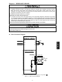
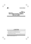
/ Instruction Manual
ENGLISH
DeviceNet Communications Card
"OPC-G1-DEV"
Fuji Electric Co., Ltd.
INR-SI47-1306b-JE
ENGLISH
English Version
Preface
Thank you for purchasing our DeviceNet Communications Card OPC-G1-DEV.
Mounting this communications card on your FRENIC-MEGA allows you to connect the FRENIC-MEGA to a
DeviceNet master unit (e.g., PC and PLC) and control it as a slave unit using the run command, speed
command, and access to function codes.
This communications card has the following features:
•
•
•
•
Data Rate (baud rate): 125 kbps, 250 kbps, 500 kbps
I/O Message:
Polling and Change of State supported
Applicable Profile:
AC Drive profile
Reading and writing all the function codes applicable to the FRENIC-MEGA (I/O Message (User Defined
Assembly Instance or Access to Function Codes Instance) and Explicit Message)
This product has been tested by ODVA authorized Independent Test Lab and found to comply with ODVA’s
DeviceNet Conformance Test Version 20.
Certification Logo Mark:
DeviceNet
is a trademark of Open DeviceNet Vendor Association, Inc. (ODVA).
This instruction manual does not contain inverter handling instructions. Read through this instruction manual in
conjunction with the FRENIC-MEGA Instruction Manual and be familiar with proper handling and operation of
this product. Improper handling might result in incorrect operation, a short life, or even a failure of this product.
Keep this manual in a safe place.
Related Publications
• RS-485 Communication User's Manual)
• FRENIC-MEGA Instruction Manual
The materials are subject to change without notice. Be sure to obtain the latest editions for use.
• Read through this instruction manual and be familiar with the DeviceNet communications card before
proceeding with installation, connections (wiring), operation, or maintenance and inspection.
• Improper handling might result in incorrect operation, a short life, or even a failure of this product as
well as the motor.
• Deliver this manual to the end user of this product. Keep this manual in a safe place until this product
is discarded.
Safety precautions
Read this manual thoroughly before proceeding with installation, connections (wiring), operation, or
maintenance and inspection. Ensure you have sound knowledge of the device and familiarize yourself with all
safety information and precautions before proceeding to operate the inverter.
Safety precautions are classified into the following two categories in this manual.
Failure to heed the information indicated by this symbol may lead to
dangerous conditions, possibly resulting in death or serious bodily
injuries.
Failure to heed the information indicated by this symbol may lead to
dangerous conditions, possibly resulting in minor or light bodily injuries
and/or substantial property damage.
Failure to heed the information contained under the CAUTION title can also result in serious consequences.
These safety precautions are of utmost importance and must be observed at all times.
1
ENGLISH
Listed below are the other materials related to the use of the DeviceNet communications card "OPC-G1-DEV."
Read them in conjunction with this manual as necessary.
Installation and wiring
• Before starting installation and wiring, turn OFF the power and wait at least five minutes for inverters
with a capacity of 22 kW or below, or at least ten minutes for inverters with a capacity of 30 kW or
above. Make sure that the LED monitor and charging lamp are turned OFF. Further, make sure,
using a multimeter or a similar instrument, that the DC link bus voltage between the terminals P(+)
and N(-) has dropped to the safe level (+25 VDC or below).
• Qualified electricians should carry out wiring.
Otherwise, an electric shock could occur.
• Do not use the product that is damaged or lacking parts.
Doing so could cause a fire, an accident, or injuries.
• Prevent lint, paper fibers, sawdust, dust, metallic chips, or other foreign materials from getting into
the inverter and the communications card.
Otherwise, a fire or an accident might result.
• Incorrect handling in installation/removal jobs could cause a failure.
A failure might result.
• Noise may be emitted from the inverter, motor and wires. Implement appropriate measure to prevent
the nearby sensors and devices from malfunctioning due to such noise.
Otherwise, an accident could occur.
Operation
• Be sure to install the front cover before turning the inverter's power ON. Do not remove the cover
when the inverter power is ON.
Otherwise, an electric shock could occur.
• Do not operate switches with wet hands.
Doing so could cause an electric shock.
• If you configure the function codes wrongly or without completely understanding FRENIC-MEGA
Instruction Manual and the FRENIC-MEGA User's Manual, the motor may rotate with a torque or at a
speed not permitted for the machine. Confirm and adjust the setting of the function codes before
running the inverter.
Otherwise, an accident could occur.
Maintenance and inspection, and parts replacement
• Before proceeding to the maintenance/inspection jobs, turn OFF the power and wait at least five
minutes for inverters with a capacity of 22 kW or below, or at least ten minutes for inverters with a
capacity of 30 kW or above. Make sure that the LED monitor and charging lamp are turned OFF.
Further, make sure, using a multimeter or a similar instrument, that the DC link bus voltage between
the terminals P(+) and N(-) has dropped to the safe level (+25 VDC or below).
Otherwise, an electric shock could occur.
• Maintenance, inspection, and parts replacement should be made only by qualified persons.
• Take off the watch, rings and other metallic objects before starting work.
• Use insulated tools.
Otherwise, an electric shock or injuries could occur.
2
Disposal
• Treat the communications card as an industrial waste when disposing of it.
Otherwise injuries could occur.
Others
• Never modify the communications card.
ENGLISH
Doing so could cause an electric shock or injuries.
Icons
The following icons are used throughout this manual.
This icon indicates information which, if not heeded, can result in the product not operating to full
efficiency, as well as information concerning incorrect operations and settings which can result in
accidents.
This icon indicates information that can prove handy when performing certain settings or operations.
This icon indicates a reference to more detailed information.
3
Table of Contents
Preface
.................................................................... 1
Safety precautions ............................................................ 1
7.3
An Example of Actual I/O Communication Data .... 24
7.3.1 Extended Speed Control Instance ................ 24
7.4 I/O Assembly Instances Assigned to Word
Variables (For reference) ....................................... 26
7.4.1 Basic Speed Control Instance ...................... 26
7.4.2 Extended Speed Control Instance ................ 26
7.4.3 Fuji Drive Assembly Instance ....................... 26
7.4.4 User Defined Assembly Instance ................. 27
7.4.5 Access to Function Codes ........................... 27
Chapter 1 BEFORE USING THE COMMUNICATIONS
CARD................................................................ 5
1.1 Acceptance Inspection ............................................ 5
1.2 Applicable Inverters ................................................. 5
Chapter 2 BASIC FUNCTIONS AND SETTINGS .............. 6
2.1 Parts Names ............................................................ 6
2.2 DIP Switch ............................................................... 6
2.3 LED Status Indicators .............................................. 7
2.4 DeviceNet Terminal Block ........................................ 7
Chapter 8 EXPLICIT MESSAGE ..................................... 28
8.1 Overview................................................................ 28
8.2 Objects to be Used in Explicit Message................. 28
8.3 Error Code List for Explicit Message Errors ........... 33
Chapter 3 INSTALLATION AND REMOVAL OF THE
COMMUNICATIONS CARD ............................. 8
3.1 Installing the Communications Card ........................ 8
3.2 Removing the Communications Card .................... 10
Chapter 9 INVERTER REACTION TO DeviceNet
COMMUNICATIONS ERRORS ...................... 34
Chapter 10 ALARM CODE LIST........................................ 35
Chapter 4 WIRING AND CABLING ..................................11
4.1 Basic Connection Diagram ..................................... 11
4.2 Wiring for DeviceNet Terminal Block ..................... 12
4.3 Wiring to Inverter ................................................... 12
Chapter 11 TROUBLESHOOTING .................................... 36
Chapter 12 SPECIFICATIONS .......................................... 37
12.1 General Specifications ......................................... 37
12.2 DeviceNet Specifications ..................................... 37
Chapter 5 CONFIGURING INVERTER'S FUNCTION
CODES FOR DeviceNet COMMUNICATION . 14
Chapter 6 ESTABLISHING A DeviceNet
COMMUNICATIONS LINK ............................. 15
Chapter 7 I/O MESSAGE ................................................ 16
7.1 Overview ............................................................... 16
7.2 I/O Assembly Instances: Selection and Setup ....... 17
7.2.1 Basic Speed Control Instance ...................... 17
7.2.2 Extended Speed Control Instance
(factory default) ............................................ 18
7.2.3 Fuji Drive Assembly Instance ....................... 19
7.2.4 User Defined Assembly Instance ................. 20
7.2.5 Access to Function Codes ........................... 22
4
Chapter 1
BEFORE USING THE COMMUNICATIONS CARD
1.1 Acceptance Inspection
Unpack the package and check the following:
(1) A communications card, two screws (M3 8), and the DeviceNet Communications Card Instruction Manual
(this manual) are contained in the package.
(2) The communications card is not damaged during transportation--no defective parts, dents or warps.
(3) The model name "OPC-G1-DEV" is printed on the communications card. (See Figure 2.1.)
If you suspect the product is not working properly or if you have any questions about your product, contact the
shop where you bought the product or your local Fuji branch office.
Neither an EDS file nor a terminating resistor comes with the communications card.
- An EDS file is required for registering the communications card to the configurator designed for
DeviceNet master node settings. It is available as a free download from our website at:
http://web1.fujielectric.co.jp/Kiki-Info-EN/User/index.html
Before downloading, you are requested to register as a member (free of charge).
- A terminating resistor of the following specifications must be used: 121 ohm ±1%, 1/4 watt,
metal-film resistor
1.2 Applicable Inverters
The DeviceNet communications card is applicable to the following inverters and ROM version.
Table 1.1 Applicable Inverter and ROM Version
Series
Inverter type
FRENIC-MEGA
G1 -
ROM version
All capacities
0500 or later
replace alphanumeric letters depending on the nominal applied motor, enclosure, power supply voltage, etc.
To check the inverter's ROM version, use Menu #5 "Maintenance Information" on the keypad. (Refer to the
FRENIC-MEGA Instruction Manual, Chapter 3, Section 3.4.6 "Reading maintenance information."
Table 1.2 Checking Inverter ROM Version
Display on LED Monitor
Item
Inverter's ROM version
Description
Shows the inverter's ROM version as a 4-digit code.
5
ENGLISH
* The boxes
FRN
Applicable motor rating
Chapter 2
BASIC FUNCTIONS AND SETTINGS
2.1 Parts Names
Figure 2.1 shows the names of the parts on the DeviceNet communications card.
Screw hole (left)
Model name
DeviceNet terminal block
LED status indicators
CN1
Release knob
(Front)
Positioning cutout
(Back)
DIP switch (SW1)
Screw hole (right)
Figure 2.1 Names of Parts on DeviceNet Communications Card (OPC-G1-DEV)
2.2 DIP Switch
The DIP switch specifies the communication data rate (baud rate) and the node address (MAC ID) on DeviceNet.
It offers a choice of three baud rates (125 kbps, 250 kbps, and 500 kbps) and a choice of node address (MAC
ID) ranging from 0 to 63.
Before accessing the DIP switch, make sure that the inverter is turned OFF.
The default configuration of the DIP switch at factory shipment is: Data rate = 500 kbps, Node address = 63.
ON
OFF
1
2
Data Rate (DR)
3
4
5
6
Node Address (NA)
7
8
DR (bps)
DIP 1-2
125K
00
250K
01
500K
10
Not
allowed
11
NA
DIP 3-8
0
000000
1
000001
2
000010
3
000011
…
…
62
111110
63
111111
Figure 2.2 DIP Switch Configuration (showing an example of Data rate = 500 kbps and Node address = 63)
6
2.3 LED Status Indicators
The communications card has two LED status indicators shown below. They indicate the status of the
communications card.
- MS (Module Status)
Indicates the hardware status of the DeviceNet communications card.
- NS (Network Status)
Indicates the communication status on DeviceNet.
The tables below show the states of the LEDs and their meanings.
Table 2.1 MS LED state
MS LED
Status
Meaning
Note
Blinks between
green and red*1
Self-diagnostic test
Running self-diagnostic test
upon power-on
This test takes 1 second.
OFF
Power OFF
Powered OFF
The inverter issues
Lights in green
Hardware normal
Hardware working normally
Lights in red
Hardware error
Communications card not
properly mounted or
hardware failure
–
The inverter issues
Table 2.2 NS LED state
NS LED
Status
Meaning
Note
Blinks between
green and red*1
Self-diagnostic test
Running self-diagnostic test
upon power-on
OFF
Offline
DeviceNet being offline
Blinks in green
Online
DeviceNet cabling correct and
communications card not
communicating on the
DeviceNet network
Lights in green
Connection established
Communications card
communicating normally on
the DeviceNet network
Connection timeout
Connection timeout between
the communications card and
the master
- Too short communication
cycle time
The inverter issues
*2
Connection error
Improper DeviceNet cabling,
or improper settings
- Node address double
assigned
- Data rate mismatch
- Bus-off state detected
- Power supply cable for the
DeviceNet unconnected
- Improper wiring for the
DeviceNet terminal block
The inverter issues
*2
Blinks in red
Lights in red
This test takes 1 second.
–
ENGLISH
Waiting for a request from
the master
–
*1 Blinks in the pattern specified in the DeviceNet specifications.
*2
cannot be reset until the NS LED comes to stay on in green. A setting for ignoring
is also available even if
a connection error is detected. For details, refer to Chapter 9 "INVERTER REACTION TO DeviceNet
COMMUNICATIONS ERRORS."
2.4 DeviceNet Terminal Block
The DeviceNet terminal block is used to connect the DeviceNet cable.
For details, refer to Chapter 4 "WIRING AND CABLING."
7
Chapter 3
INSTALLATION AND REMOVAL OF THE COMMUNICATIONS CARD
Before starting installation and wiring, turn OFF the power and wait at least five minutes for inverters with a
capacity of 22 kW or below, or at least ten minutes for inverters with a capacity of 30 kW or above. Make
sure that the LED monitor and charging lamp are turned OFF. Further, make sure, using a multimeter or a
similar instrument, that the DC link bus voltage between the terminals P(+) and N(-) has dropped to the safe
level (+25 VDC or below).
Otherwise, an electric shock could occur.
• Do not use the product that is damaged or lacking parts.
Doing so could cause a fire, an accident, or injuries.
• Prevent lint, paper fibers, sawdust, dust, metallic chips, or other foreign materials from getting into
the inverter and the communications card.
Otherwise, a fire or an accident might result.
• Incorrect handling in installation/removal jobs could cause a failure.
A failure might result.
3.1 Installing the Communications Card
Before mounting the communications card, perform the wiring for the main circuit terminals and control
circuit terminals.
(1) Remove the front cover from the inverter and expose the control printed circuit board (control PCB). As
shown in Figure 3.1, the communications card can be connected to any one of the three option connection
ports (A-, B-, and C-ports) on the inverter.
To remove the front cover, refer to the FRENIC-MEGA Instruction Manual, Chapter 2, Section 2.3.
For inverters with a capacity of 30 kW or above, open also the keypad enclosure.
(2) Insert connector CN1 on the back of the communications card (Figure 2.1) into any of the A-port (CN4),
B-port (CN5), and C-port (CN6) on the inverter's control PCB. Then tighten the two screws that come with
the card. (Figure 3.3)
Check that the positioning cutout (shown in Figure 2.1) is fitted on the tab ( in Figure 3.2) and
connector CN1 is fully inserted ( in Figure 3.2). Figure 3.3 shows the communications card
correctly mounted.
(3) Perform wiring on the communications card.
For details, refer to Chapter 4 "WIRING AND CABLING."
(4) Put the front cover back into place.
To put back the front cover, refer to the FRENIC-MEGA Instruction Manual, Chapter 2, Section 2.3.
For inverters with a capacity of 30 kW or above, close also the keypad enclosure.
8
Figure 3.1 In the case of 0.4 kW
Insert connector CN1 on the communications
card into the corresponding port on the
inverter's control PCB.
Note: Be sure to follow the order of
and .
Inserting CN1 first may lead to
insufficient insertion, resulting in a
contact failure.
Tab
Figure 3.2 Mounting the Communications Card (to B-port)
9
ENGLISH
Fit
the
positioning
cutout
of
the
communications card over the tab on the
inverter to determine the mounting position.
(Release knob)
Figure 3.3 Mounting Completed (on B-port)
3.2 Removing the Communications Card
Remove the two screws that secure the communications card and pull the release knob (shown above) to take
the communications card out of the inverter.
10
Chapter 4
WIRING AND CABLING
• Before starting installation and wiring, turn OFF the power and wait at least five minutes for inverters with
a capacity of 22 kW or below, or at least ten minutes for inverters with a capacity of 30 kW or above.
Make sure that the LED monitor and charging lamp are turned OFF. Further, make sure, using a
multimeter or a similar instrument, that the DC link bus voltage between the terminals P(+) and N(-) has
dropped to the safe level (+25 VDC or below).
• Qualified electricians should carry out wiring.
Otherwise, an electric shock could occur.
• In general, the covers of the control signal wires are not specifically designed to withstand a high voltage
(i.e., reinforced insulation is not applied). Therefore, if a control signal wire comes into direct contact with
a live conductor of the main circuit, the insulation of the cover might break down, which would expose the
signal wire to a high voltage of the main circuit. Make sure that the control signal wires will not come into
contact with live conductors of the main circuit.
Failure to observe this precaution could cause an electric shock or an accident.
Noise may be emitted from the inverter, motor and wires. Take appropriate measures to prevent the nearby
sensors and devices from malfunctioning due to such noise.
An accident could occur.
4.1 Basic Connection Diagram
L1/R
U
Motor
L2/S
V
M
L3/T
W
ENGLISH
FRENIC-MEGA
G
OPC-G1-DEV
DeviceNet
terminal block
DeviceNet cable
VTo
DeviceNet
CAN L
Shield
CAN H
V+
G*
* Mounting the communications card connects to the grounding
Figure 4.1 Basic Connection Diagram
11
G.
4.2 Wiring for DeviceNet Terminal Block
(1) To connect the communications card to DeviceNet, use a DeviceNet thin cable complying with the
DeviceNet specifications. Also observe the wiring lengths specified in the DeviceNet specifications.
The recommended DeviceNet cable is TDN24U made by SWCC Showa Device Technology, Co.,
Ltd.
Proper installation of the cable requires specialist knowledge. Be sure to refer to the DeviceNet
specifications or DeviceNet construction manual (both are published by ODVA) beforehand.
(2) Wiring around the DeviceNet terminal block (TERM1)
The terminal block uses a pluggable 5-pin connector as shown in Figure 4.2. It has five labels
corresponding to the five pins. Each label has an ID color corresponding to the wire (core) to be connected
to its pin. Make sure that the ID colors of the wires and labels match. Table 4.1 shows the correspondence
between the pin numbers and the ID colors.
A typical connector that matches this terminal block is Phoenix Contact MSTB 2.5/5-ST-5.08 AU.
The Phoenix Contact TMSTBP 2.5/5-ST-5.08 AU and TFKC 2.5/5-STF-5.08 AU (spring-cage
connection type) connectors for multidrop connection cannot be used.
Table 4.1 Pin Layout on DeviceNet Terminal Block
1
ID Color of
Wire Sheath
Pin
Assignment
1
Black
V-
Power supply
(24 VDC, - side)
2
Blue
CANL
Signal line (- side)
3
Metallic
SD
Cable shield
4
White
CANH
Signal line (+ side)
5
Red
V+
Power supply
(24 VDC, + side)
Pin #
2
3
4
5
Description
Figure 4.2
Connectors on the
DeviceNet Terminal Block
Table 4.2 lists the recommended terminal screw size and its tightening torque, and Figure 4.3 shows the
recommended strip length of the cable wire end.
Table 4.2
Recommended Tightening Torque of the
Terminal Screws for the DeviceNet Terminal Block
Terminal screw size
Tightening torque
M3
0.5 to 0.6 N·m
Cable wire
Approx.
6.0 mm
Figure 4.3 Recommended Strip Length
of the Cable Wire End for
Terminal Connection
(3) Terminating resistor
DeviceNet requires a terminating resistor to be installed externally on each end of the trunk line. Check that
the trunk line is terminated on both ends; if not, install a terminating resistor(s) on the missing end(s).
Terminating resistors do not come with the communications card. A pair of resistors with the
following specifications is separately necessary.
121 ohm ±1%, 1/4 watt, metal-film resistor
4.3 Wiring to Inverter
Route the wiring of the DeviceNet cable as far from the wiring of the main circuit as possible.
Otherwise electric noise may cause malfunctions.
Route the wires, taking care not to let them go over the control PCB, as shown in Figure 4.4.
Otherwise, malfunctions may occur.
12
• For inverters with a capacity of 22 kW or below
* Pass the wires from the communications card between the
control circuit terminal block and the front cover.
In the case of 0.4 kW
ENGLISH
• For inverters with a capacity of 30 kW or above
In the case of 75 kW
Figure 4.4 Examples of Wiring
13
Chapter 5
CONFIGURING INVERTER'S FUNCTION CODES FOR DeviceNet
COMMUNICATION
Before starting DeviceNet communication between the inverter equipped with the communications card and the
DeviceNet master device, configure the inverter's function codes listed in Table 5.1.
Table 5.2 lists other related function codes to be configured if necessary.
Table 5.1 Inverter's Function Codes for DeviceNet Communication
Function
codes
o31
*1
Factory
default
setting
Description
Select output assembly
instance
0
(From master to inverter)
o32
*1
Select input assembly
instance
0
(From inverter to master)
y98
*2
Select run/frequency
command source
0
Function code data
Remarks
Available data is:
20
: Basic speed control output
0, 21 : Extended speed control output
100 : Fuji drive assembly output
102 : User defined assembly output
104 : Request for Access to Function
Codes
See Chapter 7.
Available data is:
70
: Basic speed control input
0, 71 : Extended speed control input
101 : Fuji drive assembly input
103 : User defined assembly input
105 : Response to Function Codes
Access Request
See Chapter 7.
Available data is:
If there is no special
problem with your
system, setting y98 =
3 is recommended.
Frequency
command
Inverter
DeviceNet
Inverter
DeviceNet
0
1
2
3
Run
command
Inverter
Inverter
DeviceNet
DeviceNet
The factory default is
"Extended speed
control output."
The factory default is
"Extended speed
control input."
*1 After configuring the function code o31 or o32, restart the inverter to validate the new settings. For details about these
function codes, refer to Chapter 7 "I/O MESSAGE."
Input and output assembly instances should not be necessarily set to the same instance type. (Ex. Output assembly
instance = Extended speed control output, Input assembly instance = User defined assembly input.)
*2 If the extended speed control output is selected (o31 = 0 or 21), only bit operation in the instance can select the
run/frequency command sources, so no prior configuration of y98 is required. For details, refer to Section 7.2.2
"Extended Speed Control Instance."
Table 5.2 Other Related Function Codes
Function
codes
Description
Factory default
setting
Function code
setting range
Remarks
o27
*1
Select the inverter’s operation mode to
apply when a DeviceNet
communications error occurs.
0
0 to 15
o28
*1
Set the operation timer to apply when a
DeviceNet communications error occurs.
0.0 s
0.0 to 60.0 s
o40 to o43 Assign the function code writing data
*2 cyclically.
0
(No assignment)
o48 to o51 Assign the function code reading data
*2 cyclically.
0
(No assignment)
0000 to FFFF (hex) Valid only when
"User defined
assembly
0000 to FFFF (hex) input/output" is
selected (o31 = 102,
o32 = 103).
*1 For details about function codes o27 and o28, refer to Chapter 9 "INVERTER REACTION TO DeviceNet
COMMUNICATIONS ERRORS."
*2 For details about function codes o40 to o43 and o48 to o51, refer to Section 7.2.4 "User Defined Assembly Instance."
14
Chapter 6
ESTABLISHING A DeviceNet COMMUNICATIONS LINK
This chapter guides you to establish a DeviceNet communications link in I/O Message transmission between the
DeviceNet master and the inverter (slave).
I/O Message is a communication process that cyclically transfers data between the DeviceNet master and
slave. For details about I/O Message, refer to Chapter 7 "I/O MESSAGE."
(1) Configure the inverter's function codes described in Chapter 5.
- Set the I/O assembly instances with the inverter's function codes o31 and o32. It is not necessary to set
the same type of I/O assembly instances to input and output.
- Configure the inverter's function codes o27 and o28 with your need. If the instances for user defined
assemblies have been set, configure the function codes o40 to o43 and o48 to o51.
- After completion of the settings above, turn OFF the inverter and the communications card in order to
validate the settings.
For details about the inverter's function codes o31, o32, o40 to o43, and o48 to o51, refer to Chapter 7
"I/O MESSAGE."
(2) Set up the DeviceNet master (PLC, PC tool, or Configurator).
- Set a unique MAC ID (node address), so that it does not coincide with any other nodes.
- Set the baud rate. Make sure that all the nodes have the same baud rate.
- If necessary, install the EDS file of the communications card to the setup tool of the master.
- Allocate an I/O area corresponding to the I/O assembly instance set for the communications card. The I/O
area is either 2 words or 4 words in length.
The communications scan cycle to the communications card should be 10 ms or longer. If a single
inverter is connected to a master, the cycle should be 10 ms or longer; if two inverters are
connected, 5 ms or longer. To minimize the data conflicts and maximize the system reliability, the
cycle of 20 ms or longer is recommended.
The Electric Data Sheet (EDS) file defines parameters on the inverter. Using it quickly accesses
the desired parameters. For the communications card, the file makes it easier to access the
inverter's function codes. For how to obtain the EDS file, refer to Section 1.1 "Acceptance
Inspection."
For details about the setup procedure of the DeviceNet master, refer to the user’s manual of the
corresponding master.
(3) Configure the node address and baud rate with the DIP switch on the communications card.
- Before accessing the DIP switch, make sure that both the inverter and the communications card are
turned OFF.
- Set a unique node address, so that it does not coincide with any other nodes.
- Set the same baud rate as the master.
For details about setting the DIP switch, refer to Section 2.2 "DIP Switch."
(4) Have an I/O connection request issued from the DeviceNet master.
- Turn ON the inverter and the communications card.
- Have an I/O connection request issued from the DeviceNet master.
For details about issuing I/O connection requests from the master, refer to the user's manual of the
connected master device. In many PLCs, an I/O connection request is automatically issued at the time
of powering ON.
(5) Start I/O Message.
If both the master and the communications card have been set correctly and the wiring is proper, I/O
message connection will be established in response to the connection request and data transmission starts.
At this stage, the MS and NS LEDs on the communications card light in green. It is ready to control the
inverter according to the specified I/O assembly instances.
15
ENGLISH
- Specify the I/O connection type--"Poll" and "Change of State." Specify the communications scan cycle if
necessary.
Chapter 7
I/O MESSAGE
7.1 Overview
I/O Message is a communication process that cyclically transfers data between the DeviceNet master and the
inverter.
The communications card supports two types of I/O Message connections--Poll and Change-of-State
connections. It also supports five types of I/O assembly instances as data formats in I/O Message, as listed in
Table 7.1. One of the five instances can be selected for input and output each.
The I/O assembly instances should be specified using inverter's function codes o31 and o32.
Poll connections allow the master to periodically poll the inverter for data. In response to the request,
the inverter sends data. In Change-of-State connections, the inverter sends data only when the data
has changed.
Table 7.1 Configuring I/O Assembly Instances
Function code
o31, o32
o31=20
Type
Description
Length
(words)
20
Basic Speed Control Output
2
o31=0 or 21
21
Extended Speed Control Output
(Factory default)
2
o31=100
100
Fuji Drive Assembly Output
2
o31=102
102
User Defined Assembly Output
4
o31=104
104
Request for Access to Function Codes
4
70
Basic Speed Control Input
2
o32=0 or 71
71
Extended Speed Control Input
(Factory default)
2
o32=101
101
Fuji Drive Assembly Input
2
o32=103
103
User Defined Assembly Input
4
o32=105
105
Response to Function Codes Access
Request
4
o32=70
Output
(from master to inverter)
Instance
ID
Input
(from inverter to master)
If the "Request for Access to Function Codes" (o31=104) is selected for output, it is recommended that
the "Response to Function Codes Access Request" (o32=105) be selected for input in order to confirm
that data is correctly written in the function code. Other input and output assembly instances should
not be necessarily set to the same instance type.
(Ex. The following combination is also available:
Output assembly instance = Extended speed control output
Input assembly instance = User defined assembly input.)
Once you have modified the o31, o32, o40 to o43 and o48 to o51 data, be sure to restart the inverter
or use the RESET service to validate the new settings.
For details about the RESET service, refer to the DeviceNet's or Configurator's manual.
To stop auto tuning triggered via DeviceNet halfway, use the BX terminal command assigned to any of
digital input terminals ([X1] to [X9], [FWD] and [REV]). In the FRENIC-MEGA series of inverters, BX is
assigned to digital input terminal [X7] by factory default.
Whether the inverter has terminals [X8] and [X9] depends upon the product specifications of the
FRENIC-MEGA inverter. For details, refer to the FRENIC-MEGA Instruction Manual, Chapter 5
"FUNCTION CODES."
16
7.2 I/O Assembly Instances: Selection and Setup
7.2.1 Basic Speed Control Instance
(1) Output (from master to inverter): o31=20
Instance byte
20
bit 7
bit 6
-
bit 5
bit 4
0
-
-
-
1
(Fixed at 00)
2
Speed Reference (lower byte) (r/min)
3
Speed Reference (upper byte) (r/min)
Run Forward:
1 = Run forward command
Fault Reset:
1 = Reset the alarm condition
bit 3
-
bit 2
Fault
Reset
bit 1
-
bit 0
Run
Forward
Speed Reference: Speed command (in r/min)
(2) Input (from inverter to master): o32=70
Instance
byte
bit 7
70
0
-
1
(Fixed at 00)
2
Speed Actual (lower byte) (r/min)
3
Speed Actual (upper byte) (r/min)
-
bit 5
-
bit 4
-
bit 3
-
bit 2
Running
Forward
bit 1
-
bit 0
Faulted
1 = The inverter has (and remains) tripped
Running Forward:
1 = The motor is running forward.
Speed Actual:
Actual rotation speed (in r/min)
17
ENGLISH
Faulted:
bit 6
7.2.2 Extended Speed Control Instance (factory default)
(1) Output (from master to inverter): o31=0 or 21
Instance byte
21
bit 7
bit 6
NetRef
bit 5
0
-
NetCtrl
1
(Fixed at 00)
2
Speed Reference (lower byte) (r/min)
3
Speed Reference (upper byte) (r/min)
bit 4
-
bit 3
-
bit 2
Fault
Reset
bit 1
bit 0
Run
Reverse
Run
Forward
Run Forward:
1 = Run forward command
Run Reverse:
1 = Run reverse command
Fault Reset:
1 = Reset the alarm condition
NetCtrl:
1 = Request for enabling run command sent from DeviceNet;
0 = Request for enabling run command sent from other than DeviceNet
NetRef:
1 = Request for enabling speed reference sent from DeviceNet;
0 = Request for enabling speed reference sent from other than DeviceNet
Speed Reference:
Speed reference (in r/min)
(2) Input (from inverter to master): o32=0 or 71
Instance byte
71
bit 7
bit 6
bit 5
0
At
Ref
Reference FromNet
Ctrl
FromNet
1
Drive State
2
Speed Actual (lower byte) (r/min)
3
Speed Actual (upper byte) (r/min)
bit 4
Ready
bit 3
bit 2
Running
Reverse
Running
Forward
bit 1
-
Faulted:
Running Forward:
1 = The inverter has (and remains) tripped.
1 = The motor is running forward.
Running Reverse:
Ready:
CtrlFromNet:
1 = The motor is running backward (in the reverse direction).
1 = Ready to run
1 = Run command sent from DeviceNet being enabled
0 = Run command sent from other than DeviceNet being enabled
1 = Speed reference sent from DeviceNet being enabled
0 = Speed reference sent from other than DeviceNet being enabled
RefFromNet:
At Reference:
Drive State:
Speed Actual:
1 = The motor is running at the reference speed.
1 = Startup, 2 = Not Ready, 3 = Ready, 4 = Enabled, 5 = Stopping,
6 = Fault stop, 7 = Faulted
Actual rotation speed (in r/min)
18
bit 0
Faulted
7.2.3 Fuji Drive Assembly Instance
(1) Output (from master to inverter): o31=100
Instance
byte
bit 7
bit 6
bit 5
bit 4
bit 3
bit 2
bit 1
bit 0
100
0
X6
X5
X4
X3
X2
X1
REV
FWD
1
RST
XR
XF
-
-
X9 *
X8 *
X7
2
Frequency command p.u. (lower byte)
3
Frequency command p.u. (upper byte)
FWD:
1 = Run forward command
REV:
1 = Run reverse command
X1 to X9:
Communication terminal block command
(The function to be performed is specified by E01 to E09).
XF, XR:
Communication terminal block command
(The function to be performed is specified by E98 and E99).
RST:
1 = Reset the alarm (fault) condition.
Frequency command p.u.:
Specifies the ratio of the frequency relative to the maximum frequency
(defined by F03 in Hz) being assumed as 20000.
Frequency command p.u. = Frequency command (Hz)/F03 (Hz)
20000.
* Whether the inverter has terminals [X8] and [X9] depends upon the product specifications of the FRENIC-MEGA
inverter. For details, refer to the FRENIC-MEGA Instruction Manual, Chapter 5 "FUNCTION CODES."
(2) Input (from inverter to master): o32=101
byte
bit 7
bit 6
bit 5
bit 4
bit 3
bit 2
101
0
VL
TL
NUV
BRK
INT
EXT
REV
FWD
1
BUSY
ERR
-
RL
ALM
DEC
ACC
IL
2
Frequency output p.u. (lower byte)
3
Frequency output p.u. (upper byte)
FWD:
REV:
EXT:
During forward rotation
During reverse rotation
During DC braking (or during pre-exciting)
INT:
BRK:
NUV:
TL:
VL:
IL:
Inverter shut down
During braking
DC link bus voltage established (0 = undervoltage)
During torque limiting
During voltage limiting
During current limiting
ACC:
DEC:
ALM:
RL:
ERR:
During acceleration
During deceleration
Alarm relay (for any fault)
Run or speed command from communication enabled
Function code access error
bit 1
bit 0
BUSY:
During function code data writing
Frequency output p.u.: Output frequency monitored, relative to the maximum frequency (defined by F03
in Hz) being assumed as 20000.
19
ENGLISH
Instance
7.2.4 User Defined Assembly Instance
(1) Output (from master to inverter): o31=102
User Defined Assembly Output offers a format which allows the user to freely set or modify the function
code defined by the user using the function codes o40 to o43 beforehand. Four function codes are provided
for the user to define.
Instance byte
102
bit 7
bit 6
bit 5
bit 4
bit 3
bit 2
bit 1
0
User-defined function code 1 (write)
1
User-defined function code 1 (write) (upper byte) (data of function code specified by o40)
2
User-defined function code 2 (write) (lower byte) (data of function code specified by o41)
3
User-defined function code 2 (write) (upper byte) (data of function code specified by o41)
4
User-defined function code 3 (write) (lower byte) (data of function code specified by o42)
5
User-defined function code 3 (write) (upper byte) (data of function code specified by o42)
6
User-defined function code 4 (write) (lower byte) (data of function code specified by o43)
7
User-defined function code 4 (write) (upper byte) (data of function code specified by o43)
bit 0
(lower byte) (data of function code specified by o40)
User-defined function code 1 (write): Write data for the function code specified by o40
User-defined function code 2 (write): Write data for the function code specified by o41
User-defined function code 3 (write): Write data for the function code specified by o42
User-defined function code 4 (write): Write data for the function code specified by o43
If the same function code is assigned to more than one out of o40 to o43 codes, only the one
assigned to the smallest "o" code number becomes effective, and all the rest will be treated as
"not assigned." (For example, if the same function code is assigned to o40 and o43, o40 becomes
effective and o43 does not.)
Just like assignment of the same function code above, if S01, S05, and S19 are assigned to o40
to o43 at the same time, only the one assigned to the smallest "o" code number becomes
effective, and all the rest will be treated as "not assigned." (For example, if o40 = S05, o41 = S19,
and o42 = S01, only S05 becomes effective.)
For details about communication-dedicated function codes (S, M, W, X and Z codes), refer to the
RS-485 Communication User's Manual, Chapter 5, Section 5.2 "Data Formats."
For details about configuring the inverter's function codes using o40 to o43, refer to the next page.
(2) Input (from inverter to master): o32=103
User Defined Assembly Input offers a format which allows the user to monitor the function codes defined by
the user using the function codes o48 to o51 beforehand. Four function codes are provided for the user to
define.
Instance byte
103
bit 7
bit 6
bit 5
bit 4
bit 3
bit 2
bit 1
0
User-defined function code 1 (read) (lower byte) (data of function code specified by o48)
1
User-defined function code 1 (read) (upper byte) (data of function code specified by o48)
2
User-defined function code 2 (read) (lower byte) (data of function code specified by o49)
3
User-defined function code 2 (read) (upper byte) (data of function code specified by o49)
4
User-defined function code 3 (read) (lower byte) (data of function code specified by o50)
5
User-defined function code 3 (read) (upper byte) (data of function code specified by o50)
6
User-defined function code 4 (read) (lower byte) (data of function code specified by o51)
7
User-defined function code 4 (read) (upper byte) (data of function code specified by o51)
User-defined function code 1 (read):
User-defined function code 2 (read):
User-defined function code 3 (read):
User-defined function code 4 (read):
Monitored value of the function code specified by o48
Monitored value of the function code specified by o49
Monitored value of the function code specified by o50
Monitored value of the function code specified by o51
20
bit 0
Even modifying S05 or S19 data reflects its change into S01 only. To monitor speed in frequency
or r/min., therefore, select communication-dedicated function code M09 or M78.
For details about configuring the inverter's function codes using o48 to o51, see item (3) below.
Each function code defined has its own data format. For details about the data format of each code,
refer to the RS-485 Communication Use's Manual, Chapter 5, Section 5.2 "Data Formats."
(3) Configuring inverter's function codes o40 to o43 and o48 to o51
Specifying the function code type (shown in Table 7.2) and number in a 4-digit hexadecimal notation.
Function code number (hexadecimal)
Function code type (in accordance with Table 7.2)
Table 7.2 Function Code Type
Type
Type Code
Function Code
Type
Type Code
Function Code
2
02h
Command/function data
J
14
0Eh
Application function 1
M
3
03h
Monitored data
y
15
0Fh
Link function
F
4
04h
Fundamental function
W
16
10h
Monitored data 2
E
5
05h
Terminal function
X
17
11h
Alarm 1
C
6
06h
Control function
Z
18
12h
Alarm 2
P
7
07h
Motor 1 parameters
b
19
13h
Motor 3 parameters
H
8
08h
High performance
function
r
12
0Ch
Motor 4 parameters
A
9
09h
Motor 2 parameters
d
20
14h
Application function 2
o
10
0Ah
Optional function
Example: For F26:
F
Type Code 04
26
1A (hexadecimal)
ENGLISH
S
21
7.2.5 Access to Function Codes
(1) Request for access to function codes (from master to inverter): o31=104
This instance is provided to read or write function codes from/into the inverter.
Instance
104
byte
bit 7
bit 6
bit 5
bit 4
bit 3
X2
bit 2
bit 1
bit 0
0
X6
X5
X4
X3
X1
REV
FWD
1
RST
XR
XF
Access Code
X9 *
X8 *
X7
2
User-defined function code 1 (write) (lower byte) (data of function code specified by o40)
3
User-defined function code 1 (write) (upper byte) (data of function code specified by o40)
4
Access to function code (number)
5
Access to function code (group)
6
Access to function code (write data: lower byte)
7
Access to function code (write data: upper byte)
FWD:
REV:
X1 to X9:
1 = Run forward command
1 = Run reverse command
Communication terminal block command
(The terminal function is specified by E01 to E09).
XF, XR
Communication terminal block command
(The terminal function is specified by E98 and E99).
RST:
1 = Reset the alarm (fault) condition.
Access Code: 00, 11 = Disable, 01 = Read function codes from inverter,
10 = Write function codes into inverter
User-defined function code 1:
Specify the data of function code previously specified by o40
(For details about how to specify data, refer to Section 7.2.4 "User
Defined Assembly Instance.")
Access to function code (number): Numeral component of function code to access
Access to function code (group):
Type of function code to access (listed in Table 7.2)
Access to function code (write data): Data to write into function code specified by bytes 4 and 5
* Whether the inverter has terminals [X8] and [X9] depends upon the product specifications of the FRENIC-MEGA
inverter. For details, refer to the FRENIC-MEGA Instruction Manual, Chapter 5 "FUNCTION CODES."
Assigning any of communication-dedicated function codes S01, S06, and S19 to inverter's
function code o40 enables bytes 2 and 3 of "Request for access to function codes" instance to
specify speed.
Communication-dedicated function code S06 cannot be assigned to bytes 4 and 5. Instead, use
bytes 0 and 1 that have the similar function.
For details about communication-dedicated function codes (S, M, W, X and Z codes), refer to the
RS-485 Communication User's Manual, Chapter 5, Section 5.2 "Data Formats."
(2) Response to request for access to function codes (from inverter to master): 032=105
This instance is provided to verify the read/write result of function codes.
Instance
105
ACK:
ERR:
byte
bit 7
bit 6
bit 5
bit 4
bit 3
bit 2
bit 1
bit 0
0
VL
TL
NUV
BRK
INT
EXT
REV
FWD
1
BUSY
ERR
ACK
RL
ALM
DEC
ACC
IL
2
User-defined function code 1 (read) (lower byte) (data of function code specified by o48)
3
User-defined function code 1 (read) (upper byte) (data of function code specified by o48)
4
Access to function code (number)
5
Access to function code (group)
6
Access to function code (read data/error code: lower byte)
7
Access to function code (read data/error code: upper byte)
1=Normal response to write/read request
1=Abnormal response to write/read request
(Error code output to bytes 6 and 7)
22
User-defined function code 1: Monitored data of function code specified by o48
(e.g., speed monitor M06, M09, M79. etc.)
Access to function code (number): Value specified by "Request for access to function codes" instance
Access to function code (group):
Value specified by "Request for access to function codes" instance
Access to function code (read data): Value read from the specified function code when requested
read/write is normal
Access to function code (error code): Error code displayed (see Table 7.3) when requested read/write is
abnormal
Others:
Same as for input instance 101.
Table 7.3 Error Code List
Error code
Error name
Description
Upper
Lower
1F
02
No function code (in writing)
Attempted to write to a nonexistent function code.
03
Function code not allowed to change
Attempted to write to a read-only function code.
06
Not allowed to change in running
Attempted to write to a function code not allowed to
change when the inverter is running.
07
Not allowed to change with X terminal
being ON
Attempted to write to a function code not allowed to
change when X terminal is ON.
08
Data entry range error
Attempted to write data out of the range.
0F
Function code data being written
Requested to write to a function code being written.
21
No function code (in reading)
Attempted to read from a nonexistent function code.
(3) Examples for writing and reading to/from function codes
Normal writing and reading
ENGLISH
This example shows communication data for writing to function code F03 (=0403h) to change the data from
factory default 60.0 Hz (=0258h) to 300.0 Hz (=0BB8h) and then reading from F03. (The following data is
expressed in hexadecimal.)
Select the inverter's function code F03.
Write: 00 00 00 00 03 04 00 00
Read: 28 10 00 00 00 00 00 00
Input data to F03.
Write: 00 00 00 00 03 04 B8 0B
Read: 28 10 00 00 00 00 00 00
Write data into F03.
Write: 00 10 00 00 03 04 B8 0B
Read: 28 10 00 00 03 04 B8 0B
Read from F03.
Write: 00 08 00 00 03 04 00 00
Read: 28 10 00 00 03 04 B8 0B
Reading/writing error
This example shows communication data that returns an error code since writing and reading to/from
nonexistent function code F99 (=0463h) is attempted.
Select the inverter's function code F99.
Write: 00 00 00 00 63 04 00 00
Read: 28 10 00 00 00 00 00 00
Write data into F99.
Write: 00 10 00 00 63 04 00 00
Read: 28 50 00 00 63 04 02 1F
Read from F99.
Write: 00 08 00 00 63 04 00 00
Read: 28 50 00 00 63 04 21 1F
23
7.3 An Example of Actual I/O Communication Data
7.3.1 Extended Speed Control Instance
Presented herein is an actual communication data in the format of Extended Speed Control Instance, the factory
default format.
(1) Driving pattern example
Given below is an example of the driving pattern for controlling the inverter. Its corresponding I/O data is
shown in (2) below.
Forward
1800 r/min
Time (s)
300 r/min
1800 r/min
Reverse
Figure 7.1 Driving Pattern
(2) Description of I/O Data (The I/O data are in hexadecimal notation.)
Request:
Run command is OFF. Speed command = 1800 r/min (= 0708h). The run command and speed
command via DeviceNet are enabled.
60 00 08 07
Response: Stopping. The inverter is ready.
70 03 00 00
Request:
Run forward command. Speed command = 1800 r/min (= 0708h). The run command and speed
command via DeviceNet are enabled.
61 00 08 07
Response: The motor is running forward and accelerating. The actual speed is increasing.
74 04 ** **
Request:
Run forward command. Speed command = 1800 r/min (= 0708h). The run command and speed
command via DeviceNet are enabled.
61 00 08 07
Response: Running forward. The actual speed has reached the Reference
F4 04 08 07
Request:
Run command is OFF. Speed command = 1800 r/min (= 0708h). The run command and speed
command via DeviceNet are enabled.
60 00 08 07
Response: The motor is running forward and decelerating. The actual speed is decreasing.
74 05 ** **
Request:
No run command. Speed command is changed to 300 r/min (= 012Ch). The run command and
speed command via DeviceNet are enabled.
60 00 2C 01
Response: Stopping. The inverter is ready.
70 03 00 00
Request:
Run reverse command. Speed command = 300 r/min (= 012Ch). The run command and speed
command via DeviceNet are enabled.
62 00 2C 01
Response: The motor is running backward (in the reverse direction) and accelerating. The actual speed is
increasing.
78 04 ** **
24
Request:
Run reverse command. Speed command = 300 r/min (= 012Ch). The run command and speed
command via DeviceNet are enabled.
62 00 2C 01
Response: Running in the reverse direction. The actual speed has reached Reference
F8 04 2C 01
Request:
Run reverse command. Speed command is changed to 1800 r/min (= 0708h). The run
command and speed command via DeviceNet are enabled.
62 00 08 07
Response: The motor is running backward (in the reverse direction) and accelerating. The actual speed is
increasing.
78 04 ** **
Request:
Run reverse command. Speed command = 1800 r/min (= 0708h). The run command and speed
command via DeviceNet are enabled.
62 00 08 07
Response: Running in the reverse direction. The actual speed has reached Reference
F8 04 08 07
Run command is OFF. Speed command = 1800 r/min (= 0708h). The run command and speed
command via DeviceNet are enabled.
60 00 08 07
Response: The motor is running backward (in the reverse direction) and decelerating. The actual speed is
decreasing.
78 05 ** **
ENGLISH
Request:
25
7.4 I/O Assembly Instances Assigned to Word Variables (For reference)
Some masters assign an I/O assembly instance area to a word variable. Shown below are the formats for each
I/O assembly instance assigned to a word variable. For details about the definition of bits in the formats, refer to
Section 7.2 "I/O Assembly Instances: Selection and Setup."
7.4.1 Basic Speed Control Instance
(1) Output (from master to inverter): o31=20
word bit 15
0
-
1
14
13
12
11
10
9
8
7
6
5
4
3
-
-
-
-
-
-
-
-
-
-
-
-
2
1
bit 0
Fault
Reset
-
Run
Forward
Speed Reference (r/min)
(2) Input (from inverter to master): o32=70
word bit 15
0
14
13
12
11
10
9
8
7
6
5
4
3
2
1
bit 0
-
-
-
-
-
-
-
-
-
-
-
-
Running
Forward
-
Faulted
-
1
Speed Actual (r/min)
7.4.2 Extended Speed Control Instance
(1) Output (from master to inverter): o31=0 or 21
word bit 15
0
14
13
12
11
10
9
8
7
6
5
4
3
-
-
-
-
-
-
-
-
Net
Ref
Net
Ctrl
-
-
-
1
2
1
bit 0
Fault Run
Run
Reset Reverse Forward
Speed Reference (r/min)
(2) Input (from inverter to master): o32=0 or 71
word bit 15 14
0
-
1
13
12
11
10
9
8
7
6
5
-
-
-
-
-
-
At
Reference
*2
*1 Ready Running Running
Reverse Forward
-
4
3
2
1
bit 0
-
Faulted
Speed Actual (r/min)
*1 CtrlFromNet
*2 RefFromNet
7.4.3 Fuji Drive Assembly Instance
(1) Output (from master to inverter): o31=100
word
bit 15
14
13
12
11
10
9
8
7
6
5
4
3
2
0
RST
XR
XF
-
-
X9 *
X8 *
X7
X6
X5
X4
X3
X2
X1
1
1
bit 0
REV FWD
Frequency command p.u.
* Whether the inverter has terminals [X8] and [X9] depends upon the product specifications of the FRENIC-MEGA
inverter. For details, refer to the FRENIC-MEGA Instruction Manual, Chapter 5 "FUNCTION CODES."
(2) Input (from inverter to master): o32=101
word
0
1
bit 15
14
13
12
BUSY
ERR
-
RL
11
10
9
ALM DEC ACC
8
7
6
IL
VL
TL
Frequency command p.u.
26
5
4
NUV BRK
3
2
INT
EXT
1
bit 0
REV FWD
7.4.4 User Defined Assembly Instance
(1) Output (from master to inverter): o31=102
word
bit 15
14
13
12
11
10
9
8
7
6
5
0
User-defined function code 1 (write) (data of function code specified by o40)
1
User-defined function code 2 (write) (data of function code specified by o41)
2
User-defined function code 3 (write) (data of function code specified by o42)
3
User-defined function code 4 (write) (data of function code specified by o43)
4
3
2
1
bit 0
4
3
2
1
bit 0
(2) Input (from inverter to master): o32=103
word
bit 15
14
13
12
11
10
9
8
7
6
5
0
User-defined function code 1 (read) (data of function code specified by o48)
1
User-defined function code 2 (read) (data of function code specified by o49)
2
User-defined function code 3 (read) (data of function code specified by o50)
3
User-defined function code 4 (read) (data of function code specified by o51)
7.4.5 Access to Function Codes
(1) Request for access to function codes (from master to inverter): o31=104
bit 15
14
13
12
11
10
0
RST
XR
XF
1
User-defined function code 1 (write) (data of function code specified by o40)
2
Access to function code (group) + Access to function code (number) (Refer to Table 7.2.)
3
Access to function code (write data)
Access code X9 *
9
8
7
6
5
4
3
2
X8 *
X7
X6
X5
X4
X3
X2
X1
1
bit 0
REV FWD
* Whether the inverter has terminals [X8] and [X9] depends upon the product specifications of the FRENIC-MEGA
inverter. For details, refer to the FRENIC-MEGA Instruction Manual, Chapter 5 "FUNCTION CODES."
(2) Response to request for access to function codes (from inverter to master): o32=105
word
bit 15
14
13
12
11
10
9
8
7
6
5
4
3
2
0
BUSY ERR
ACK
RL
ALM
DEC
ACC
IL
VL
TL
NUV
BRK
INT
EXT
1
User-defined function code 1 (read) (data of function code specified by o48)
2
Access to function code (group) + Access to function code (number) (Refer to Table 7.2.)
3
Access to function code (read data/error code)
27
1
bit 0
REV FWD
ENGLISH
word
Chapter 8
EXPLICIT MESSAGE
8.1 Overview
Explicit Message is a communication process that accesses DeviceNet variables at arbitrary (event-driven)
timing. Using the communications card is capable of accessing not only standard DeviceNet variables but also
all inverter's function codes. Explicit Message lacks realtime performance, but it allows many variables to be set
or referred to. It is, therefore, suited for initial setting.
Refer to the user's manual of the connected master for Explicit Message.
- Variables usable in Explicit Message are grouped using three codes--Class (major key), Instance
(medium key) and Attribute (minor key). These three codes should be used for specifying a variable.
- A group of all variables contained in Class is called "Object."
8.2 Objects to be Used in Explicit Message
This section describes objects relating to the communications card and the inverter. Other objects that are
automatically executed by the master device are excluded in this manual.
(1) Identity object (Class 01 hex.)
This object refers to the product information of the communications card. It is a group of read-only variables.
Instance
1
Attribute
Name
Description
Value (hex.)
R/W
Data size
01
Vender ID
Manufacturer's ID code
013F (=319):
Fuji Electric Group
R
Word
02
Device Type
Applied device profile
0002: AC drive
R
Word
03
Product Code
ID code of the
communications card
2403
R
Word
04
Revision
Software version
(Major and minor versions)
Display of version
Example: 01, 0A
(=Ver. 1.10)
R
Byte,
Byte
05
Status
Status of the communications
card
Depends on DeviceNet
specifications.
R
Word
06
Serial Number
Serial number of the product
Differs with the product.
R
DWord
07
Product Name
Model name
OPC-G1-DEV
R
11 bytes
(2) Motor Data object (Class 28 hex.)
This object refers to and sets up the motor rated current and voltage. When Motor 2, 3, or 4 is selected, this
object automatically switches to the one for Motor 2, 3, or 4.
For details about motor switching, refer to the FRENIC-MEGA Instruction Manual, Chapter 5, Section 5.2
"Details of Function Codes."
Instance
Attribute
Name
Description
1
03
Motor Type
Type of motor to be
connected
06
Rated Current
07
Rated Voltage
R/W
Data size
07: Squirrel-cage,
induction motor
R
Byte
Rated current in units of 0.1 A
Depends on the
inverter setting.
R/W
Word
Rated voltage in units of 1 V
(base voltage)
Depends on the
inverter setting.
R/W
Word
28
Value (hex.)
(3) Control Supervisor object (Class 29 hex.)
This object monitors the current run command settings and the running status of the inverter, and configures the
running-related settings.
1
Attribute
Name
Description
Value (hex.)
R/W
Data size
03
Run1
Run forward command
00: OFF
01: ON
R/W
Byte
04
Run2
Run reverse command
00: OFF
01: ON
R/W
Byte
05
NetCtrl
Switching run command
source
00: Inverter
01: DeviceNet
R/W
Byte
06
State
Current inverter status
01: Inverter running
02: Inverter not ready to
run
03: Inverter ready to run
04: Inverter running
05: During deceleration
06: Stop due to
communication broken
07: Tripped
R
Byte
07
Running1
Running forward
00: Stopped/Running
reverse
01: Running forward
R
Byte
08
Running2
Running reverse
00: Stopped/Running
forward
01: Running reverse
R
Byte
09
Ready
Inverter ready to run/
Inverter running
(Synchronized with State
above)
00: State = Value except
below
01: State = 03 to 05
R
Byte
0A
Faulted
Tripped state
00: Not tripped
01: Tripped
R
Byte
0B
Warning
Warning. Fixed at 0.
00: No warning
R
Byte
0C
FaultRst
Reset of tripped (alarm) state
00 01: Request for reset
R/W
Byte
0F
CtrlFromNet
Current run command source
00: Inverter
01: DeviceNet
R
Byte
10
DNFaultMode Inverter reaction to DeviceNet Refer to Chapter 9.
communications errors
R/W
Byte
29
ENGLISH
Instance
(4) AC/DC Drive object (Class 2A hex.)
This object monitors the current speed command settings and the current speed of the inverter, and configures
their related settings. It also monitors the output data issued from the inverter.
Instance
Attribute
Name
Description
Value (hex.)
R/W
Data size
1
03 hex
AtReference
Speed arrival
00: Stopped or
Accelerating/
decelerating
01: Speed arrival
R
Byte
04 hex
NetRef
Switching speed command
source
00: Inverter
01: DeviceNet
R/W
Byte
06 hex
DriveMode
Run mode. Fixed at 0.
00: Unique to vendor
R
Byte
07 hex
SpeedActual
Speed monitor (r/min)
Actual speed
R
Word
08 hex
SpeedRef
Speed command (r/min)
-32768 to 32767 r/min
R/W
Word
09 hex
CurrentActual
Output current
(in units of 0.1 A)
Output current
R
Word
11 hex
OutputVoltage
Output voltage (V)
Output voltage
R
Word
12 hex
AccelTime
Acceleration time (ms)
0 to 65535 ms
R/W
Word
13 hex
DeccelTime
Deceleration time (ms)
0 to 65535 ms
R/W
Word
14 hex
LowSpdLimit
Lower limit speed (r/min)
0 to 32767 r/min
R/W
Word
15 hex
HighSpdLimit
Maximum speed (r/min)
0 to 32767 r/min
R/W *
Word
16 hex
SpeedScale
Change the speed scale
(r/min) all at once, as
calculated below.
-15 to 15
(Factory default: 0)
R/W
Byte
-15 to 15
(Factory default: 0)
R/W
Byte
-15 to 15
(Factory default: 0)
R/W
Byte
-15 to 15
(Factory default: 0)
R/W
Byte
00: Inverter
01: DeviceNet
R
Byte
r/min
2
17 hex
CurrentScale
SpeedScale
Change the current scale
(0.1 A) all at once, as
calculated below.
0.1 A
2
1B hex
VoltageScale
CurrentSca le
Change the voltage scale (V)
all at once, as calculated
below.
V
2
1C hex
TimeScale
VoltageSca le
Change the time scale (ms)
all at once, as calculated
below.
ms
2
1D hex
RefFromNet
TimeScale
Current speed command
source
* "Read-only" while the inverter is running.
30
(5) Inverter Function Code object (Class 64 hex.)
This object configures or refers to inverter's function codes.
Instance corresponds to function code group and Attribute, to function code number.
Example: To configure F26 data, specify 04 hex for Instance and 1A hex (=26) for Attribute.
Instance
Attribute
Name
Description
Value (hex.)
R/W
Data size
02
01
S01
Communication function code S01
0 to FFFF
R/W
Word
(S codes)
:
:
:
:
:
:
:
:
:
:
:
:
63 hex (99)
S99
Communication function code S99
0 to FFFF
R/W
Word
03
01
M01
Communication function code M01
0 to FFFF
R
Word
(M codes)
:
:
:
:
:
:
:
:
:
:
63 hex (99)
M99
0 to FFFF
R
Word
04
01
F01
Inverter function code F01
0 to FFFF
R/W
Word
(F codes)
:
:
:
:
:
:
:
:
:
:
:
:
63 hex (99)
F99
Inverter function code F99
0 to FFFF
R/W
Word
05
01
E01
Inverter function code E01
0 to FFFF
R/W
Word
(E codes)
:
:
:
:
:
:
:
:
:
:
:
:
63 hex (99)
E99
Inverter function code E99
0 to FFFF
R/W
Word
06
01
C01
Inverter function code C01
0 to FFFF
R/W
Word
(C codes)
:
:
:
:
:
:
:
:
:
:
:
:
63 hex (99)
C99
Inverter function code C99
0 to FFFF
R/W
Word
07
01
P01
Inverter function code P01
0 to FFFF
R/W
Word
(P codes)
:
:
:
:
:
:
:
:
:
:
:
:
63 hex (99)
P99
Inverter function code P99
0 to FFFF
R/W
Word
08
01
H01
Inverter function code H01
0 to FFFF
R/W
Word
(H codes)
:
:
:
:
:
:
:
:
:
:
:
:
63 hex (99)
H99
Inverter function code H99
0 to FFFF
R/W
Word
09
01
A01
Inverter function code A01
0 to FFFF
R/W
Word
(A codes)
:
:
:
:
:
:
:
:
:
:
:
:
63 hex (99)
A99
Inverter function code A99
0 to FFFF
R/W
Word
0A (10)
01
o01
Option function code o01
0 to FFFF
R/W
Word
(o codes)
:
:
:
:
:
:
:
:
:
:
:
:
63 hex (99)
o99
Option function code o99
0 to FFFF
R/W
Word
0E (14)
01
J01
Inverter function code J01
0 to FFFF
R/W
Word
(J codes)
:
:
:
:
:
:
:
:
:
:
:
:
63 hex (99)
J99
Inverter function code J99
0 to FFFF
R/W
Word
:
:
Communication function code M99
31
ENGLISH
Inverter's function codes have individually specified data formats. For details about the data formats, refer
to the RS-485 Communication User's Manual, Chapter 5 "Function Codes and Data Formats." For details
about function code data, refer to the FRENIC-MEGA Instruction Manual, Chapter 5 "FUNCTION
CODES."
Instance
Attribute
Name
Description
Value (hex.)
R/W
Data size
0F (15)
01
y01
Inverter function code y01
0 to FFFF
R/W
Word
(y codes)
:
:
:
:
:
:
:
:
:
:
:
:
63 hex (99)
y99
Inverter function code y99
0 to FFFF
R/W
Word
10 (16)
01
W01
Communication function code W01
0 to FFFF
R
Word
(W codes)
:
:
:
:
:
:
:
:
:
:
:
:
63 hex (99)
W99
Communication function code W99
0 to FFFF
R
Word
11 (17)
01
X01
Communication function code X01
0 to FFFF
R
Word
(X codes)
:
:
:
:
:
:
:
:
:
:
:
:
63 hex (99)
X99
Communication function code X99
0 to FFFF
R
Word
12 (18)
01
Z01
Communication function code Z01
0 to FFFF
R
Word
(Z codes)
:
:
:
:
:
:
:
:
:
:
:
:
63 hex (99)
Z99
Communication function code Z99
0 to FFFF
R
Word
13 (19)
01
b01
Inverter function code b01
0 to FFFF
R/W
Word
(b codes)
:
:
:
:
:
:
:
:
:
:
63 hex (99)
b99
Inverter function code b99
0 to FFFF
R/W
Word
0C (12)
01
r01
Inverter function code r01
0 to FFFF
R/W
Word
(r codes)
:
:
:
:
:
:
:
:
:
:
63 hex (99)
r99
Inverter function code r99
0 to FFFF
R/W
Word
14 (20)
01
d01
Inverter function code d01
0 to FFFF
R/W
Word
(d codes)
:
:
:
:
:
:
:
:
:
:
:
:
63 hex (99)
d99
Inverter function code d99
0 to FFFF
R/W
Word
:
:
:
:
32
8.3 Error Code List for Explicit Message Errors
If an explicit message sent from the master contains any error, the communications card responds to the master
with "94" in the service code and "error code" (see Table 8.1) in the data.
An error code is two bytes long, consisting of a general code and additional code. Some error codes have no
additional code and have "FF" instead.
Table 8.1 Error Code List for Explicit Message Errors
Error code
Additional
code
Error name
08
FF
Service not supported
Invalid service code
Correct service code.
(Read: 0E hex, Write: 10 hex)
0E
FF
Invalid attribute value
Attempted to change a
write-inhibited variable.
Check the specified variable
again.
13
FF
Not enough data
Attempted to write Byte
data to Word variable.
Match the data size.
14
FF
Attribute not supported
Access to a nonexistent
variable.
Check the specified variable
again.
15
FF
Too much data
Attempted to write Word
data to Byte variable.
Match the data size.
16
FF
Object does not exist
Access to a nonexistent
object.
Correct the contents of the
Class.
1F
See blow.
Vender specific error
Error unique to vendor
See below.
02
No function code
(in writing)
Attempted to write to a
nonexistent function code.
Correct the function code
number specified.
03
Function code not
allowed to change
Attempted to write to a
read-only function code.
Correct the function code
number specified.
06
Not allowed to change
in running
Attempted to write to a
function code not allowed to
change when the inverter is
running.
Write after the inverter is
stopped.
07
Not allowed to change
with X terminal being
ON
Attempted to write to a
function code not allowed to
change when X terminal is
ON.
Write after the X terminal is
turned OFF.
08
Data entry range error
Attempted to write data out
of the range.
Write data within the range.
0F
Function code data
being written
Requested to write to a
function code being written.
Request to write after
completion of the current writing
operation.
21
No function code
(in reading)
Attempted to read from a
nonexistent function code.
Correct the function code
number specified.
FF
Invalid parameter
Attempted to write a value
out of the range.
Correct the value within the
range.
20
Description
33
Error recovery
ENGLISH
General
code
Chapter 9
INVERTER REACTION TO DeviceNet COMMUNICATIONS ERRORS
Inverter's function codes o27 and o28 specify the inverter reaction to be taken after an error occurrence. Table
9.1 lists the settings for o27 and o28. The same setting can also be made by the DeviceNet variable
DNFaultMode (Class: 0x29, Instance: 0x01, Attribute: 0x10).
Table 9.2 lists the inverter reaction specified by the DNFaultMode. The setting value of o27 and that of
DNFaultMode are interlocked with each other. Changing either one automatically changes the other one.
Table 9.1 Inverter Reactions to DeviceNet Communications Errors Specified by Function Codes o27 and o28
o27 data
o28 data
Inverter reaction to DeviceNet communications error
0,
4 to 9
---
1
0.0 s to 60.0 s
After the time specified by o28, coast to a stop and trip
with
.
2
0.0 s to 60.0 s
If the communications link is restored within the time
specified by o28, ignore the communications error. After
the timeout, coast to a stop and trip with
.
3,
13 to 15
---
Keep the current operation, ignoring the communications
error. (No
trip)
10
---
Immediately decelerate to a stop.
Issue
after stopping.
The inverter's function code
F08 specifies the
deceleration time.
11
0.0 s to 60.0 s
After the time specified by o28, decelerate to a stop. Issue
after stopping.
Same as above.
12
0.0 s to 60.0 s
If the communications link is restored within the time
specified by o28, ignore the communications error. After
the timeout, decelerate to a stop and trip with
.
Same as above.
13
---
Immediately run command OFF. (No
14
---
Force to rotate the motor in forward direction.
(No
trip)
Forward rotation is enabled
when NetCtrl = 1.
15
---
Force to rotate the motor in reverse direction.
(No
trip)
Reverse rotation is enabled
when NetCtrl = 1.
Immediately coast to a stop and trip with
Remarks
.
trip)
Table 9.2 Inverter Reactions to DeviceNet Communications Errors Specified by DNFaultMode
DNFaultMode
Inverter reaction to DeviceNet communications error
Remarks
trip)
o27 data
0
Immediately run command OFF. (No
13
1
Ignore the communications error. (No
2
If the communications link is restored within the time
specified by o28, ignore the communications error. After
the timeout, decelerate to a stop and trip with
.
The inverter's function code
F08 specifies the deceleration
time.
12
3
Force to rotate the motor in forward direction.
(No
trip)
Forward rotation is enabled
when NetCtrl = 1.
14
4
Force to rotate the motor in reverse direction.
(No
trip)
Reverse rotation is enabled
when NetCtrl = 1.
15
trip)
3
100
Immediately coast to a stop and trip with
0
101
After the time specified by o28, coast to a stop and trip
with
.
1
102
If the communications link is restored within the time
specified by o28, ignore the communications error. After
the timeout, coast to a stop and trip with
.
2
110
Immediately decelerate to a stop.
Issue
after stopping.
The inverter's function code
F08 specifies the deceleration
time.
10
111
After the time specified by o28, decelerate to a stop.
Issue
after stopping.
Same as above.
11
112
Same as for [DNFaultMode = 2]
.
12
34
Chapter 10 ALARM CODE LIST
The information on alarms that have occurred in the inverter can be monitored through DeviceNet.
They are stored in the inverter's function codes M16 to M19 as listed in Table 10.1.
The communication-dedicated function codes M16 to M19 store information on the latest alarm code, last alarm
code, 2nd last alarm code, and 3rd last alarm code, respectively.
Table 10.1 Alarm Codes
Alarm codes
in
M16 to M19
Description
0 (00H)
No alarm
1 (01H)
---
Description
29 (1DH)
NTC thermistor wire break
Overcurrent
(during acceleration)
31 (1FH)
Memory error
2 (02H)
Overcurrent
(during deceleration)
32 (20H)
Keypad communications error
3 (03H)
Overcurrent
(During running at constant
speed)
33 (21H)
CPU error
5 (05H)
Grounding fault
34 (22H)
Option communications error
6 (06H)
Overvoltage
(during acceleration)
35 (23H)
Option error
7 (07H)
Overvoltage
(during deceleration)
36 (24H)
Operation protection
8 (08H)
Overvoltage
(during running at constant
speed or stopped)
37 (25H)
Tuning error
10 (0AH)
Undervoltage
38 (26H)
RS-485 communications error
(COM port 1)
11 (0BH)
Input phase loss
44 (2CH)
Overload of motor 3
14 (0EH)
Fuse blown
45 (2DH)
Overload of motor 4
16 (10H)
Charger circuit fault
46 (2EH)
Output phase loss
17 (11H)
Heat sink overheat
47 (2FH)
Speed mismatch
(Excessive speed deviation)
18 (12H)
External alarm
51 (33H)
Data saving error during
undervoltage
19 (13H)
Inverter internal overheat
53 (35H)
RS-485 communications error
(COM port 2)
20 (14H)
Motor protection
(PTC/NTC thermistor)
54 (36H)
Hardware error
22 (16H)
Braking resistor overheat
56 (38H)
Positioning control error
23 (17H)
Overload of motor 1
57 (39H)
EN circuit failure
24 (18H)
Overload of motor 2
58 (3AH)
PID feedback wire break
25 (19H)
Inverter overload
59 (3BH)
Braking transistor broken
27 (1BH)
Overspeed
28 (1CH)
PG wire break
254 (FEH)
35
Mock alarm
ENGLISH
Alarm codes
in
M16 to M19
Chapter 11 TROUBLESHOOTING
If any problem or error occurs during DeviceNet communication, follow the troubleshooting procedures given
below.
No
Phenomenon/Symptom
1
None of the LEDs on the
communications card would
light.
2
alarm cannot be reset
(The MS LED lights in red).
Probable Causes
The communications card is not properly mounted.
The communications card is faulty.
The communications card is not properly mounted.
The communications card is faulty.
Other type of communications card is mounted.
The same node address is double assigned in DeviceNet.
There is a mismatch in baud (data) rate.
3
The NS LED lights in red.
(
alarm cannot be reset.)
The network power (24 V) is not properly supplied.
Cabling for DeviceNet communications is not properly done.
The inverter has not restarted after modification of the DIP switch
configuration.
4
The NS LED blinks in red.
(
alarm has occurred.)
5
The NS LED would not light.
The cable was broken during communication.
The I/O scan interval is too short.
The node address for the communications card is improper.
The cable for DeviceNet communications was broken.
The master does not request a connection.
6
The NS LED keeps blinking in
green and does not come to
stay on in green.
The I/O scan interval has been set to be too short at the start of
communication.
The I/O area is invalidly mapped.
There is no I/O connection.
Neither NetCtrl nor NetRef is set to "1."
7
8
Even though the NS LED
lights in green, the settings for
run command or speed
command cannot be
validated.
Although the speed command
has been validated, the actual
speed is different from it.
On the inverter, the higher-priority run command or speed
command is enabled.
There is a mistake in the selection of I/O Assembly Instances.
The inverter has not restarted after modification of any of the o31
and o40 to o43 data.
Refer to the FRENIC-MEGA Instruction Manual, Chapter 6,
Section 6.3.1 "Motor is running abnormally."
36
Chapter 12 SPECIFICATIONS
12.1 General Specifications
Install the inverter equipped with the communications card in an environment that satisfies the requirements
listed below.
Item
Specifications
Site location
Indoors
Surrounding temperature
Refer to the FRENIC-MEGA Instruction Manual, Chapter 2.
Relative humidity
5 to 95% (No condensation)
Atmosphere
The inverter must not be exposed to dust, direct sunlight, corrosive gases,
flammable gases, oil mist, vapor or water drops.
Pollution degree 2 (IEC60664-1) (Note)
The atmosphere can contain a small amount of salt.
(0.01 mg/cm2 or less per year)
The inverter must not be subjected to sudden changes in temperature that will
cause condensation to form.
Altitude
1,000 m max.
Atmospheric pressure
86 to 106 kPa
Vibration
Refer to the FRENIC-MEGA Instruction Manual, Chapter 2.
(Note) Do not install the inverter in an environment where it may be exposed to lint, cotton waste or moist dust or dirt
which will clog the heat sink of the inverter. If the inverter is to be used in such an environment, install it in a
dustproof panel of your system.
12.2 DeviceNet Specifications
Specifications
Network input voltage
11 to 25 V
Network power consumption
75 mA at maximum (24 VDC)
ENGLISH
Item
(Note) The network power is supplied by an external power source.
No. of nodes connected
64 at maximum (including the master)
MAC ID
0 to 63
Insulation
500 VDC (photocoupler insulation)
Transmission rate
500 kbps/250 kbps/125 kbps
Maximum cable length
Transmission rate
(Trunk line: thick cable
Drop line: thin cable)
Trunk line length
Drop line length
Total length of drop lines
500 kbps
250 kbps
125 kbps
100 m
250 m
500 m
6m
6m
6m
39 m
78 m
156 m
Messages supported
1. I/O Message (Poll, Change of State)
2. Explicit Message
Vendor ID
319 (Fuji Electric Group)
Device type
AC drive (code: 2)
Product code
9219
Model name
OPC-G1-DEV
Applicable device profile
AC Drive
No. of input/output bytes
Selectable between 4 and 8 bytes for input and output (independently)
Applicable DeviceNet
Specifications
CIP Specifications Volume 1, Edition 2.2 Japanese version and Volume
3, Edition 1.1 Japanese version
(Certified by ODVA Japan for Conformance Test Version 20)
Node type
Group 2 only server
37
MEMO
DeviceNet Communications Card
"OPC-G1-DEV"
Instruction Manual
First Edition, June 2008
Third Edition, April 2011
Fuji Electric Co., Ltd.
The purpose of this manual is to provide accurate information in the handling, setting up and operating of
the DeviceNet communications card for the FRENIC-MEGA series of inverters. Please feel free to send
your comments regarding any errors or omissions you may have found, or any suggestions you may have
for generally improving the manual.
In no event will Fuji Electric Co., Ltd. be liable for any direct or indirect damages resulting from the
application of the information in this manual.
Fuji Electric Co., Ltd.
Gate City Ohsaki, East Tower, 11-2, Osaki 1-chome,
Shinagawa-ku, Tokyo, 141-0032, Japan
URL http://www.fujielectric.co.jp/
Phone: +81 3 5435 7283 Fax: +81 3 5435 7425
URL http://www.fujielectric.com/
2011-04 (D11b/F08) 1CM